EP3443636B1 - Cell balancing method and system - Google Patents
Cell balancing method and system Download PDFInfo
- Publication number
- EP3443636B1 EP3443636B1 EP17733350.7A EP17733350A EP3443636B1 EP 3443636 B1 EP3443636 B1 EP 3443636B1 EP 17733350 A EP17733350 A EP 17733350A EP 3443636 B1 EP3443636 B1 EP 3443636B1
- Authority
- EP
- European Patent Office
- Prior art keywords
- balancing
- battery
- module
- cell
- modules
- Prior art date
- Legal status (The legal status is an assumption and is not a legal conclusion. Google has not performed a legal analysis and makes no representation as to the accuracy of the status listed.)
- Active
Links
Images


Classifications
-
- H—ELECTRICITY
- H02—GENERATION; CONVERSION OR DISTRIBUTION OF ELECTRIC POWER
- H02J—CIRCUIT ARRANGEMENTS OR SYSTEMS FOR SUPPLYING OR DISTRIBUTING ELECTRIC POWER; SYSTEMS FOR STORING ELECTRIC ENERGY
- H02J7/00—Circuit arrangements for charging or depolarising batteries or for supplying loads from batteries
- H02J7/0013—Circuit arrangements for charging or depolarising batteries or for supplying loads from batteries acting upon several batteries simultaneously or sequentially
- H02J7/0014—Circuits for equalisation of charge between batteries
-
- H—ELECTRICITY
- H02—GENERATION; CONVERSION OR DISTRIBUTION OF ELECTRIC POWER
- H02J—CIRCUIT ARRANGEMENTS OR SYSTEMS FOR SUPPLYING OR DISTRIBUTING ELECTRIC POWER; SYSTEMS FOR STORING ELECTRIC ENERGY
- H02J7/00—Circuit arrangements for charging or depolarising batteries or for supplying loads from batteries
- H02J7/0013—Circuit arrangements for charging or depolarising batteries or for supplying loads from batteries acting upon several batteries simultaneously or sequentially
-
- H—ELECTRICITY
- H02—GENERATION; CONVERSION OR DISTRIBUTION OF ELECTRIC POWER
- H02J—CIRCUIT ARRANGEMENTS OR SYSTEMS FOR SUPPLYING OR DISTRIBUTING ELECTRIC POWER; SYSTEMS FOR STORING ELECTRIC ENERGY
- H02J7/00—Circuit arrangements for charging or depolarising batteries or for supplying loads from batteries
- H02J7/0047—Circuit arrangements for charging or depolarising batteries or for supplying loads from batteries with monitoring or indicating devices or circuits
- H02J7/0048—Detection of remaining charge capacity or state of charge [SOC]
-
- H—ELECTRICITY
- H02—GENERATION; CONVERSION OR DISTRIBUTION OF ELECTRIC POWER
- H02J—CIRCUIT ARRANGEMENTS OR SYSTEMS FOR SUPPLYING OR DISTRIBUTING ELECTRIC POWER; SYSTEMS FOR STORING ELECTRIC ENERGY
- H02J7/00—Circuit arrangements for charging or depolarising batteries or for supplying loads from batteries
- H02J7/0029—Circuit arrangements for charging or depolarising batteries or for supplying loads from batteries with safety or protection devices or circuits
- H02J7/00302—Overcharge protection
-
- H—ELECTRICITY
- H02—GENERATION; CONVERSION OR DISTRIBUTION OF ELECTRIC POWER
- H02M—APPARATUS FOR CONVERSION BETWEEN AC AND AC, BETWEEN AC AND DC, OR BETWEEN DC AND DC, AND FOR USE WITH MAINS OR SIMILAR POWER SUPPLY SYSTEMS; CONVERSION OF DC OR AC INPUT POWER INTO SURGE OUTPUT POWER; CONTROL OR REGULATION THEREOF
- H02M3/00—Conversion of DC power input into DC power output
- H02M3/22—Conversion of DC power input into DC power output with intermediate conversion into AC
- H02M3/24—Conversion of DC power input into DC power output with intermediate conversion into AC by static converters
- H02M3/28—Conversion of DC power input into DC power output with intermediate conversion into AC by static converters using discharge tubes with control electrode or semiconductor devices with control electrode to produce the intermediate AC
- H02M3/325—Conversion of DC power input into DC power output with intermediate conversion into AC by static converters using discharge tubes with control electrode or semiconductor devices with control electrode to produce the intermediate AC using devices of a triode or a transistor type requiring continuous application of a control signal
- H02M3/335—Conversion of DC power input into DC power output with intermediate conversion into AC by static converters using discharge tubes with control electrode or semiconductor devices with control electrode to produce the intermediate AC using devices of a triode or a transistor type requiring continuous application of a control signal using semiconductor devices only
- H02M3/33569—Conversion of DC power input into DC power output with intermediate conversion into AC by static converters using discharge tubes with control electrode or semiconductor devices with control electrode to produce the intermediate AC using devices of a triode or a transistor type requiring continuous application of a control signal using semiconductor devices only having several active switching elements
-
- Y—GENERAL TAGGING OF NEW TECHNOLOGICAL DEVELOPMENTS; GENERAL TAGGING OF CROSS-SECTIONAL TECHNOLOGIES SPANNING OVER SEVERAL SECTIONS OF THE IPC; TECHNICAL SUBJECTS COVERED BY FORMER USPC CROSS-REFERENCE ART COLLECTIONS [XRACs] AND DIGESTS
- Y02—TECHNOLOGIES OR APPLICATIONS FOR MITIGATION OR ADAPTATION AGAINST CLIMATE CHANGE
- Y02T—CLIMATE CHANGE MITIGATION TECHNOLOGIES RELATED TO TRANSPORTATION
- Y02T10/00—Road transport of goods or passengers
- Y02T10/60—Other road transportation technologies with climate change mitigation effect
- Y02T10/70—Energy storage systems for electromobility, e.g. batteries
Definitions
- the present invention relates generally to systems and methods for cell balancing in battery systems and more specifically to such systems and methods that apply a combination of active and passive cell balancing in order to optimize cell balancing under different conditions.
- Cell balancing systems and methods are known within the art of battery management and such systems and methods are vital in optimizing the performance of batteries composed of a large number of cells such as those required in electrochemical storage systems of medium and large scale, for instance designed to operate in electric vehicles.
- Documents dealing with cell balancing are: EP2787954 A2 , US2008/0090133 A1 , US2002/0011820 A1 , EP1289096 A2 , US2006/022639 A1 , EP2075892 A2 .
- the main purpose of such systems and methods is to maintain homogeneous conditions between all cells of the battery, thus allowing optimal operation in terms of efficiency, stored energy and lifetime.
- cells are connected in series. If the cells are perfectly balanced, the total voltage will be equally divided per cell. However, in practice, the cells will be unbalanced.
- Cell balancing process equalizes the charge on all the cells in the chain and thus increasing battery capacity. This process is required because maximum charge is limited by the highest cell voltage, and maximum discharge is limited by the lowest. Its use is desirable in almost every technology (the only exception is the technology Redox-Flow) and is essential in some cases as in ion-lithium batteries.
- batteries in a series string may not operate in a uniform manner.
- Batteries are inter alia characterized by their internal resistance, which can vary within certain tolerance limits of a given type of battery cell. Batteries with more efficient cells (i.e. with cells having a relatively low internal resistance) tend to have a higher voltage while batteries with less efficient cells remain at a lower voltage. Once the imbalance occurs, it will tend to increase with additional usage. Thus, when charging batteries, some reach full charge long before others. Likewise, weaker cells will tend to discharge much more rapidly than the rest of the pack. This leads to under-utilization of most of the cells. In summary, when these imbalanced batteries are left in use without any control, such as cell equalization, the energy storage capacity decreases severely.
- HEVs hybrid electric vehicles
- electric scooters uninterruptible power supplies.
- an HEV battery is severely exposed to a charge and discharge environment. This exposure occurs because an HEV can recover energy from the wheels during regenerative braking (an energy source that was wasted in the past) and reuse it to propel the vehicle at low speeds or provide extra power for high acceleration. This repeated charge and discharge phenomenon aggravates the cell mismatch problem.
- the imbalances between cells can be defined in terms of voltage or SOC (state of charge).
- SOC state of charge
- the benefits obtained by using equalization systems comprise (i) extension of the life span of the battery system; (ii) increased efficiency of the battery system; (iii) increased usable energy of the battery system; and (iv) improved operation safety of the battery system.
- Active cell balancing is the method to apply when dissipation of cell energy as heat is to be avoided. Active cell balancing is more efficient than passive cell balancing and does not give raise to the generation of heat and hence makes it possible to apply higher balancing currents than passive balancing.
- active cell balancing helps to take advantage of the energy stored in the specific module by raising the SOC of cells having a SOC below the average of that specific module up to the average value and thus allowing to discharge the full module until the minimum allowed SOC for almost every cell, instead of being limited by just one cell that reaches the minimum SOC floor.
- active balancing can be used too.
- Passive cell balancing can for instance be applied advantageously (at least) in the following situations: During the end of a charge process passive balancing can be used in order to reduce the SOC of a single or a few cells that are above the SOC average value of the module and then finish the charging process with all the cells at their maximum SOC possible. If during the charging process, only a relatively few cells are insufficiently charged, active balancing can be applied in order to raise their state of charge rapidly. On the contrary, if a relatively few cells are charged above their maximum allowable state of charge, passive balancing can advantageously be applied.
- the system comprises a passive module balancing means coupled between the positive and negative terminals of the specific module.
- the active cell balancing means is a flyback DC/DC converter.
- the passive cell balancing means is a resistor in series with a switch, such as for instance a MOSFET.
- the passive module balancing means is a resistor in series with a switch, such as for instance a MOSFET.
- the flyback DC/DC converter extracts power from all of the cells (C 1 , C 2 ,....C N ) of a module, and injects a controlled current to balance the most discharged cell until it is in balance with the other cells.
- the controlled current is constant.
- the microcontroller is a microcontroller in a battery management system (BMS) that manages the overall performance of the battery.
- BMS battery management system
- active balancing as applied in the modules making up a battery
- passive balancing is applied between modules making up the battery
- the system comprises module state of charge (SOC) monitoring means or voltage monitoring means that monitors the SOC or voltage of the modules in a battery and when an imbalance between the SOC or voltage is detected between two or more modules, passive balancing between the two or more modules in the battery is performed.
- SOC module state of charge
- the passive balancing between two or more modules in a battery is controlled by the hybrid module balancing block or the battery management system (BMS).
- BMS battery management system
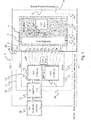
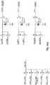
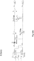
- FIG 1 there is shown an embodiment of a cell balancing system according to the present invention generally indicated by reference numeral 1 comprising means for applying a combination of active and passive cell balancing.
- the system shown in figure 1 comprises a battery module that in the shown embodiment contains a series connection of ten cells C1, C2, ... C10. It is of cause understood that a different number of cells could be present in the module and that the principles of the invention would apply equally well to such modules.
- module is used repeatedly in the description of the embodiment shown in figure 1 , the present invention is not restricted to one or more physical modules making up a total battery.
- a battery could thus simply comprise a number of cells coupled in series without any subdivision into specific modules or a module may simply be a fictive subdivision of a given number of cells in a battery.
- reference to the term “module” implies no restriction to the scope of the present invention.
- the system comprises a hybrid module balancing block 3 that comprises a switching array 4, a passive balancing means, such as the resistor 5 that can be activated through a controllable switch 6, such as a MOSFET, and an active balancing device, such as a DC/DC converter 7.
- a hybrid module balancing block 3 that comprises a switching array 4, a passive balancing means, such as the resistor 5 that can be activated through a controllable switch 6, such as a MOSFET, and an active balancing device, such as a DC/DC converter 7.
- a module passive balancing means such as the resistor 8 that can be activated through the switch 9, such as a MOSFET.
- the switching array 4, the cell passive balancing means 5 and 6, the DC/DC converter 7 and the module passive balancing means 8 and 9 are controlled by appropriate control signals, as symbolically indicated be control lines 20 through 25.
- the voltages over each respective cells C1 through C10 are measured by means of a cells monitoring block 15 that in the shown embodiment comprises the two ASIC's 16 and 17 connected to the terminals of the respective cells through cell voltage measuring lines Vcells.
- the flyback converter can be controlled from the main microcontroller in the battery management system (BMS).
- BMS battery management system
- An example of such a microcontroller is the HERCULES MCU 32-bit ARM Cortex R4 manufactured by Texas Instruments.
- the system and method according to the present invention can be implemented in the BMS main microcontroller, but could alternatively be implemented in a separate microcontroller.
- the controlling microcontroller is in the shown embodiment designated by reference numeral 18 and is in connection with the ASIC's 16 and 17 in the cells monitoring block 15 through the serial peripheral interfaces SPI.
- the microcontroller 18 receives a signal indicating the positive module voltage Vmod+ via signal line 12 and a signal indication the negative module voltage Vmod- via signal line 13. Further, the microcontroller 18 received a signal indicating the output current Imod 26 from the module via signal line 11. The output current 26 is measured by suitable means as symbolically indicated by 25. The microcontroller 18 provides, based inter alia on these signals the control signal 20 to the various functional blocks of the balancing system, i.e. the control signals 21, 22, 23 and 24.
- This Switched DC/DC converter that is used in the shown embodiment of the invention is based on a "Module to Cell" topology and allows, without too much extra costs, to monitor the current injected on each cell while balancing, thus enabling to obtain a better SOC considering the current injected during the balancing process.
- the DC/DC Converter 7 is an isolated flyback converter that extracts the power from all the module cells (C1 through C10 in the embodiment shown in figure 1 ) and injects a controlled constant current (CC) to balance the most discharged cell until it is in balance with the other cells.
- the connection of the isolated flyback converter to the most discharged cell is done with an array of relays 4 and only one can be switched at the same time to avoid dangerous short circuits.
- the design of the DC/DC converter that can be used in embodiments of the invention is described in some detail in the following.
- the converter can as mentioned above for example be implemented into the HERCULES microcontroller, if desired.
- the converter control needs an analog signal for measuring the balancing current (and close the feedback loop for control), a PWM digital output, and a digital output per cell (built using an external de-multiplexing system) to activate the switches that connect the DC/DC converter to the cell that requires balancing.
- the Switched DC/DC converter according to an embodiment of the invention is based on a "Module to Cell" topology and allows, without limited extra costs, to monitor the current injected on each cell while balancing, thus making it possible to obtain a more optimal state of charge (SOC) considering the current injected during the balancing process.
- SOC state of charge
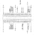
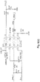
- FIG 2 there is shown a flowchart illustrating an embodiment of a cell balancing method according to the invention that can for instance be applied for a battery comprising one or more modules, each comprising a number of cells, as for instance shown in figure 1 .
- the balancing method is initiated at step 27 and a given battery module is chosen at step 28.
- step 29 it is determined by appropriate means if a charging process is in taking place and if this is the case the method proceeds to step 30, thereby applying active cell balancing between cells in the given module, i.e. the module chosen in step 28.
- step 31 Towards the end of the charging it may happen that one or a few cells of the given module are charged above a predefined upper limit L u of SOC or cell voltage. If this is detected in step 31, according to the embodiment of the method shown in figure 2 , that this or these cells are charged above the predefined upper limit L u , passive cell balancing is applied to these cells in step 32 in order to reduce their charge to the required value. If it is determined in step 31 the no cells are above the upper limit the process proceeds to step 33 in which it is determined if further modules that have to be charged are present in the battery, after which the above described process is repeated for the next module.
- step 34 determines if there is an imbalance between the SOC of voltage between modules. If this is the case, the process applies either passive or active balancing between modules, for instance (in case of passive balancing) by means of the resistor 8 shown in figure 1 . This inter module balancing proceeds until a required balance between modules have been obtained, after which the process terminates in step 38.
- the upper limit L u can be determined and provided as indicated by 39 to the functional step 31.
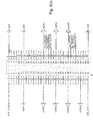
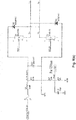
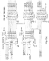
- FIG 3a and b there is shown a schematic circuit diagram of an embodiment of an isolated flyback converter circuitry (MOSFETS, filters, isolation transformer, etc.), where the flyback Control block and the cell C1, C2 and C3 connected to the output of the flyback converter. It is noted that other numbers of cells than the three actually shown in the figure could be used according to the invention. There are other parts in the schematic used to measure currents and voltages all along the circuit. The energy needed to correct the unbalance status of one specific cell is obtained from all the cells of the module and is then injected on that specific cell.
- MOSFETS isolated flyback converter circuitry
- the DC/DC converter topology is an isolated flyback converter, acting like a buck converter with isolation.
- the PWM signal allows controlling the output current and voltage of the DC/DC converter.
- An objective of the system and method of the present invention is to re-charge the unbalanced cell with a controlled current, for instance a 1A current, that is extracted from the full array of cells that composes a module.
- a controlled current for instance a 1A current
- the simulation schematic includes filtering and discretization of the output current feedback measurement. This resembles the way an analog stage and an Analog to Digital Converter (ADC) work in a real electronic system. Also, the flyback control block works in the way it is expected to work in the HERCULES microcontroller, this means that the control code is executed one time for each sample acquisition of the analog signal.
- ADC Analog to Digital Converter
- the sampling frequency has in the results of the simulations shown in the following been set to 2kHz and the resolution of the ADCs is 12 bits .
- the output current will be sensed using a shunt resistor (in this example 50mOhm) and an instrumentation amplifier (for instance INA282) with a fixed gain of 50x in the results shown in the following.
- the PWM switching frequency has been set at 100kHz, but other switching frequencies could also be used.
- flyback_Control block that implements the control algorithm that allows re-charging a specific cell from its initial unbalanced state up to the desired balanced state.
- the parameters needed to control the start-stop and current injection are:
- flyback_Control block There are other control parameters in the flyback_Control block related with the simulation process in PSIM (fs) and PI regulator parameters (Kp, Ki) for controlling the output current.
- the flyback_Control block is in an embodiment programmed in C code to make it easily portable to the HERCULES microcontroller, but it is understood that other programing languages could alternatively be used.
- the Hercules ⁇ C generates the PWM signal, switch (relay) selection signals, possible passive balancing activation signal/signals? for the full module and receives the feedback of the balancing output current signal to close the control loop.
- the PWM signal will control? the isolated flyback DC/DC converter in order to generate the desired amount (magnitude) of current to re-charge the selected cell.
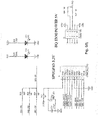
- FIG. 5a through g there is shown the interface with the Hercules ⁇ C evaluation board, and also the power supply needed to generate the different supply levels, including the isolated voltage (such as 5V) needed for the output current and cell voltage measuring operational amplifiers.
- the schematic in figure 2 also shows the interface components needed to manage the different voltage levels in all the signals present in this embodiment of the invention.
- the analog and digital signals can be routed to different pins in the ⁇ C to allow compatibility with different combinations and configurations.
- connection with the TI BQ76PL536EVM is done with an SPI bus and some digital signals, and it is present in connector J1 and J2.
- the Dual Switch isolated flyback converter To manage both MOSFETs PWM signal, the IC U114 (UCC27201) acts as a High and Low Gate Driver, receiving the PWM signal from the ⁇ C.
- the current sensor used to send the current signal to the microcontroller is in this embodiment a combination of a 25mOhm shunt resistor and two analog amplifiers.
- the first one in the chain is the AMC1200-Q1. It is a balanced isolation amplifier with a fixed gain of 8x and it is powered with 5V by the TMV-1205SHI isolated DC/DC converter.
- the balanced output of this isolation amplifier is amplified again by the INA332 (11x for the current measurement and 5x for the voltage measurement). Both signals are given to the HERCULES ⁇ C ADC inputs on leq_Out and Veq_Out ports.
- the Module voltage is also measured by the resistor divider network and is given to the uC on Vmod port.
- a Wurth WE750312503 isolation transformer for the flyback converter that works between 36V and 72V input voltage is used.
- the selected topology is the dual switch flyback and the MOSFETs reference is STN2NF10.
- the output diode D19 (PMEG3030EP) has been selected for its low Vf to reduce conduction looses.
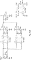
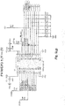
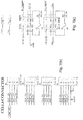
- FIG. 7a through g there is shown an embodiment of a Relay selection circuitry provided with de-multiplexer to avoid having 2 relays connected at the same time to different parts of the cell that would lead to a short circuit between two or more cells.
- the selection of the relay that connects one single cell to the flyback output is done with a logic circuitry based on SN74HC238D de-multiplexers. In this way it is ensured that only one single relay is activated at the same time, avoiding dangerous short-circuits between cells.
- the relay is driven by a ULQ2003A darlington array that manages the relay coil activation.
- relays There last two relays (RLY17 and RLY18) are in this embodiment used to connect a resistor in series with a single cell or with the full module to allow passive balancing and thus obtaining the Hybridized Balancing prototype.
- the relay selected for this application is the IMR6
- the HERCULES ⁇ C has been configured and programmed in order to control the flyback converter, using the following peripherals:
- the uC peripherals are configured as follows:
- the HERCULES ⁇ C With the ePWM module the HERCULES ⁇ C generates a PWM signal capable to control the flyback converter. With the HET Module a signal is generated to trigger the conversion of the ADC at an appropriate frequency, such as 2kHz, which captures the measured value of the current sensor. The ⁇ C receives the analog signal from the current sensor in order to close the control loop, performing as a PI controller. Using the GPIO of the Port A, the ⁇ C selects the cell to be recharged. If desired, the ⁇ C also enables the passive balancing for one cell or for the full module.
- Tests have been carried out with the Dual Switch flyback converter charging one Cell at a fixed and controlled current of 1A.
- the core of the active balancing circuitry is the isolated flyback converter.
- the flyback converter is controlled by the HERCULES ⁇ C with a PWM signal (ETPWM 6B pin) and the control loop is feed by the analog signal that corresponds with the output current (AD1IN2 pin).
- the HERCULES uC is able to select the cell that needs to be recharged thanks to the logic circuitry attached to GIOA port.
- Lines GIOA0 to GIOA3 are used to select the cell from 1 to 16 and GIOA5 is used to enable the output from the 3.3V-to-5V buffer and GIOA4 is used to enable the output of the de-multiplexers. Both enable signals are active low signals.
- the ⁇ C starts to control the PWM signal of the flyback converter in order to recharge the selected cell at 1A rate.
- the cell model used in these tests is the Kokam SLPB90255255H.
- the precision of the output current value is ⁇ 1.5%.
- the efficiency of the power conversion in the flyback converter is above 82.5% in most input/output conditions, arriving to efficiency peaks of around 87.5% when the input voltage is around 55V.
- Passive balancing has also been tested by connecting one 4 ⁇ resistor (5W) to discharge a single cell at a rate of around 1A, and one 68 ⁇ resistor (100W) to discharge the full 16 cell module at a rate of around 1A. It is understood that different resistor values could be used and that passive balancing could be carried out by other means than by resistors.
- FIG 8 there is shown results obtained for a simulation of a balancing process of 1 cell that needs to go from a 90% SOC until a 95%SOC.
- the input voltage for the flyback is 64.45V, equivalent to 16 cells where 15 cells are charged at SOC 95% and 1 cell is charged at 90%. This last cell is the one that will be balanced.
- the current "loutDC" is increased until it reaches 1A and then remains steady until the SOC reaches a charge of 95%, then it stops.
- SOC_1 SOC_1
- VoutDC Cell Voltage
- FIG 9 there is shown results obtained for a simulation of a balancing process of 1 cell that needs to be charged from a 90% SOC until a 95% SOC.
- the input voltage for the flyback is 32.18V, equivalent to 8 cells where 7 cells are charged at 95% SOC and 1 cell is charged at 90%. This last cell is the one that will be balanced. The rest of the signals are the same as for the results shown in figure 8 ..
- the controlled flyback power supply according to an embodiment of the invention is able to recharge the specific cell at a constant current of 1A until its SOC reaches the desired value.
Landscapes
- Engineering & Computer Science (AREA)
- Power Engineering (AREA)
- Charge And Discharge Circuits For Batteries Or The Like (AREA)
- Secondary Cells (AREA)
Priority Applications (1)
| Application Number | Priority Date | Filing Date | Title |
|---|---|---|---|
| PL17733350T PL3443636T3 (pl) | 2016-04-16 | 2017-04-12 | Sposób i układ balansowania ogniw |
Applications Claiming Priority (2)
| Application Number | Priority Date | Filing Date | Title |
|---|---|---|---|
| DKPA201600228A DK179053B1 (en) | 2016-04-16 | 2016-04-16 | Cell balancing method and system |
| PCT/DK2017/000007 WO2017178023A1 (en) | 2016-04-16 | 2017-04-12 | Cell balancing method and system |
Publications (2)
| Publication Number | Publication Date |
|---|---|
| EP3443636A1 EP3443636A1 (en) | 2019-02-20 |
| EP3443636B1 true EP3443636B1 (en) | 2020-09-23 |
Family
ID=59227424
Family Applications (1)
| Application Number | Title | Priority Date | Filing Date |
|---|---|---|---|
| EP17733350.7A Active EP3443636B1 (en) | 2016-04-16 | 2017-04-12 | Cell balancing method and system |
Country Status (8)
| Country | Link |
|---|---|
| US (1) | US10938222B2 (enExample) |
| EP (1) | EP3443636B1 (enExample) |
| JP (1) | JP7123807B2 (enExample) |
| CN (1) | CN108886264B (enExample) |
| DK (1) | DK179053B1 (enExample) |
| ES (1) | ES2837537T3 (enExample) |
| PL (1) | PL3443636T3 (enExample) |
| WO (1) | WO2017178023A1 (enExample) |
Cited By (1)
| Publication number | Priority date | Publication date | Assignee | Title |
|---|---|---|---|---|
| DE102024000329B3 (de) | 2024-02-01 | 2025-03-27 | Mercedes-Benz Group AG | Batterie und Fahrzeug |
Families Citing this family (16)
| Publication number | Priority date | Publication date | Assignee | Title |
|---|---|---|---|---|
| DK179053B1 (en) | 2016-04-16 | 2017-09-18 | Lithium Balance As | Cell balancing method and system |
| KR102123048B1 (ko) * | 2017-01-10 | 2020-06-15 | 주식회사 엘지화학 | 에너지 절약 및 빠른 셀 밸런싱이 가능한 충전 제어 장치 및 방법 |
| KR102236384B1 (ko) * | 2017-10-27 | 2021-04-05 | 주식회사 엘지화학 | 배터리 밸런싱을 위한 장치 및 그것을 포함하는 배터리팩 |
| WO2019123906A1 (ja) * | 2017-12-19 | 2019-06-27 | 三洋電機株式会社 | 管理装置、及び電源システム |
| CN111033938A (zh) * | 2018-01-30 | 2020-04-17 | 松下知识产权经营株式会社 | 车辆用电源系统、管理装置 |
| WO2020022344A1 (ja) * | 2018-07-25 | 2020-01-30 | 三洋電機株式会社 | 電源システム、及び管理装置 |
| US10978884B2 (en) * | 2018-08-10 | 2021-04-13 | Powin Energy Corporation | Enhanced switched balancing network for battery pack |
| US11063444B2 (en) * | 2018-08-10 | 2021-07-13 | Powin, Llc | Enhanced battery management system for battery pack |
| WO2020055809A1 (en) | 2018-09-11 | 2020-03-19 | Powin Energy Corporation | Modular battery stack and support system |
| CN114072983A (zh) * | 2019-05-16 | 2022-02-18 | 特洛斯公司 | 用于双均衡电池和电池组性能管理的方法和系统 |
| KR102321029B1 (ko) * | 2019-09-16 | 2021-11-03 | 호남대학교 산학협력단 | 클러스터링을 이용한 이종의 전력 밸런싱을 수행하기 위한 시스템, 이를 위한 장치 및 이를 위한 방법 |
| KR102373716B1 (ko) * | 2020-07-15 | 2022-03-17 | 한국철도기술연구원 | 배터리 모듈의 셀 밸런싱 장치 |
| CN112736999A (zh) * | 2020-11-30 | 2021-04-30 | 浙江大有实业有限公司杭州科技发展分公司 | 具有多个反激式变换器的串联电池均衡装置 |
| CN113933617B (zh) * | 2021-09-07 | 2024-07-30 | 南京南瑞继保电气有限公司 | 一种有源型模块化换流器试验系统及控制方法 |
| CN114899906A (zh) * | 2022-05-09 | 2022-08-12 | 华为数字能源技术有限公司 | 电池系统的控制电路装置及电池管理系统 |
| KR20250053319A (ko) * | 2023-10-13 | 2025-04-22 | 주식회사 한국엘에프피 | 배터리 충방전 회로 시스템 |
Family Cites Families (38)
| Publication number | Priority date | Publication date | Assignee | Title |
|---|---|---|---|---|
| US5710504A (en) * | 1996-05-20 | 1998-01-20 | The Board Of Trustees Of The University Of Illinois | Switched capacitor system for automatic battery equalization |
| JP3922655B2 (ja) * | 1996-07-12 | 2007-05-30 | 株式会社東京アールアンドデー | 電源装置の制御システムおよび電源装置の制御方法 |
| US6417648B2 (en) * | 2000-06-28 | 2002-07-09 | Nissan Motor Co., Ltd. | Method of and apparatus for implementing capacity adjustment in battery pack |
| JP4605952B2 (ja) * | 2001-08-29 | 2011-01-05 | 株式会社日立製作所 | 蓄電装置及びその制御方法 |
| US20040137326A1 (en) * | 2002-11-09 | 2004-07-15 | Munshi M. Zafar A. | Lithium ion battery and methods of manufacturing same |
| JP2005151720A (ja) | 2003-11-17 | 2005-06-09 | Mitsubishi Heavy Ind Ltd | セルバランス補正装置、二次電池、セルバランス補正方法及びセルバランス補正プログラム |
| US7126312B2 (en) * | 2004-07-28 | 2006-10-24 | Enerdel, Inc. | Method and apparatus for balancing multi-cell lithium battery systems |
| KR100778414B1 (ko) * | 2006-10-12 | 2007-11-22 | 삼성에스디아이 주식회사 | 배터리 관리 시스템 및 그의 구동 방법 |
| US8350529B2 (en) * | 2006-11-10 | 2013-01-08 | Lithium Balance A/S | Battery management system |
| WO2008137764A1 (en) * | 2007-05-03 | 2008-11-13 | Sendyne Corporation | Fine-controlled battery-charging system |
| KR101107999B1 (ko) * | 2007-10-16 | 2012-01-25 | 한국과학기술원 | 전압 센서와 전하 균일 장치가 결합된 배터리 운용 시스템 |
| US8030895B2 (en) | 2007-12-27 | 2011-10-04 | Fenghua Xiao | Cell balancing systems with multiple controllers |
| US8748727B2 (en) * | 2008-01-18 | 2014-06-10 | Tenksolar, Inc. | Flat-plate photovoltaic module |
| US8207740B2 (en) * | 2009-06-23 | 2012-06-26 | GM Global Technology Operations LLC | Method for use with a vehicle battery pack having a number of individual battery cells |
| WO2011034957A2 (en) * | 2009-09-16 | 2011-03-24 | National Semiconductor Corporation | Active cell and module balancing for batteries or other power supplies |
| JP2011072153A (ja) | 2009-09-28 | 2011-04-07 | Sanyo Electric Co Ltd | 車両用電源装置及びこれを備える車両並びに車両用電源装置の容量均等化方法 |
| JP5143185B2 (ja) * | 2010-02-08 | 2013-02-13 | 三洋電機株式会社 | 電源装置 |
| WO2012145319A1 (en) * | 2011-04-20 | 2012-10-26 | A123 Systems, Inc. | System and method for balancing charge between battery cells |
| US20120274283A1 (en) * | 2011-04-28 | 2012-11-01 | Van Lammeren Johannes | Battery cell-balancing method and apparatus |
| US9153973B2 (en) * | 2011-06-13 | 2015-10-06 | Mehmet Kadri Nalbant | Active cell balancing |
| EP2541728A2 (en) * | 2011-06-30 | 2013-01-02 | Kabushiki Kaisha Toyota Jidoshokki | Cell balancing device |
| JP5821619B2 (ja) * | 2011-12-26 | 2015-11-24 | ソニー株式会社 | 電力貯蔵装置、電力システムおよび電動車両 |
| US9293928B2 (en) * | 2013-04-23 | 2016-03-22 | Kevin Alexander | System and method for a dynamically configurable power distribution control and management system |
| US20140097787A1 (en) * | 2012-10-09 | 2014-04-10 | Yi-Ming Lin | Active battery management system for a battery pack |
| US9281696B2 (en) * | 2013-02-27 | 2016-03-08 | Fu-Sheng Tsai | Current steering circuit and current steering method for controlling branch current flowing through branch |
| WO2014156564A1 (ja) * | 2013-03-28 | 2014-10-02 | 日本電気株式会社 | 蓄電池及び蓄電池の動作方法 |
| TWI627812B (zh) * | 2013-04-05 | 2018-06-21 | 美商線性科技股份有限公司 | 電壓補償主動電池平衡的裝置、系統及方法 |
| US20140340023A1 (en) * | 2013-05-17 | 2014-11-20 | Ying-Haw Shu | Hybrid battery balancing system |
| US9531038B2 (en) * | 2013-07-31 | 2016-12-27 | Dell Products, Lp | System and method of cell block voltage analytics to improve balancing effectiveness and identify self-discharge rate |
| US9168836B2 (en) * | 2013-12-13 | 2015-10-27 | Powin Energy Corporation | Non-traction battery controller and applications thereof |
| US10305298B2 (en) * | 2014-03-17 | 2019-05-28 | Glx Power Systems, Inc. | Method and apparatus for creating a dynamically reconfigurable energy storage device |
| CN107076801B (zh) * | 2014-07-25 | 2020-10-02 | 锂平衡公司 | 电池管理系统中的电化学阻抗谱 |
| DE102014221867A1 (de) * | 2014-10-27 | 2016-04-28 | Robert Bosch Gmbh | Verfahren und Schaltungsanordnung zum aktiven Cell-Balancing eines elektrischen Energiespeichers |
| CN104442437B (zh) * | 2014-11-19 | 2017-11-17 | 北京新能源汽车股份有限公司 | 一种兼具均衡功能的电动汽车优化能源系统 |
| US10931123B2 (en) * | 2015-03-04 | 2021-02-23 | Maxwell Technologies, Inc. | Systems and methods for improving cell balancing and cell failure detection |
| GB2541419B (en) * | 2015-08-18 | 2017-11-29 | Oxis Energy Ltd | Monitoring and balancing capacity in lithium sulfur cells arranged in series |
| DK179053B1 (en) | 2016-04-16 | 2017-09-18 | Lithium Balance As | Cell balancing method and system |
| JP7126498B2 (ja) * | 2016-11-07 | 2022-08-26 | コーバス エナジー インコーポレイテッド | マルチセルバッテリの均等化 |
-
2016
- 2016-04-16 DK DKPA201600228A patent/DK179053B1/en active
-
2017
- 2017-04-12 WO PCT/DK2017/000007 patent/WO2017178023A1/en not_active Ceased
- 2017-04-12 JP JP2018554384A patent/JP7123807B2/ja active Active
- 2017-04-12 EP EP17733350.7A patent/EP3443636B1/en active Active
- 2017-04-12 US US16/093,859 patent/US10938222B2/en active Active
- 2017-04-12 PL PL17733350T patent/PL3443636T3/pl unknown
- 2017-04-12 CN CN201780023207.2A patent/CN108886264B/zh active Active
- 2017-04-12 ES ES17733350T patent/ES2837537T3/es active Active
Non-Patent Citations (1)
| Title |
|---|
| None * |
Cited By (2)
| Publication number | Priority date | Publication date | Assignee | Title |
|---|---|---|---|---|
| DE102024000329B3 (de) | 2024-02-01 | 2025-03-27 | Mercedes-Benz Group AG | Batterie und Fahrzeug |
| WO2025163113A1 (de) | 2024-02-01 | 2025-08-07 | Mercedes-Benz Group AG | Batterie und fahrzeug |
Also Published As
| Publication number | Publication date |
|---|---|
| DK179053B1 (en) | 2017-09-18 |
| JP7123807B2 (ja) | 2022-08-23 |
| PL3443636T3 (pl) | 2021-05-31 |
| DK201600228A1 (en) | 2017-09-18 |
| ES2837537T3 (es) | 2021-06-30 |
| CN108886264B (zh) | 2023-01-24 |
| US10938222B2 (en) | 2021-03-02 |
| EP3443636A1 (en) | 2019-02-20 |
| US20190109468A1 (en) | 2019-04-11 |
| WO2017178023A1 (en) | 2017-10-19 |
| CN108886264A (zh) | 2018-11-23 |
| JP2019514332A (ja) | 2019-05-30 |
Similar Documents
| Publication | Publication Date | Title |
|---|---|---|
| EP3443636B1 (en) | Cell balancing method and system | |
| CN101174711B (zh) | 电池管理系统及其驱动方法 | |
| US10680447B2 (en) | Charge equalization apparatus for a battery string | |
| EP1798100B1 (en) | Battery management system | |
| CN100546148C (zh) | 调节电池soc的方法和使用该方法的电池管理系统 | |
| CN101563827B (zh) | 组电池控制方法、组电池控制电路以及具备该组电池控制电路的充电电路、电池组件 | |
| CN103534897B (zh) | 电池控制装置 | |
| EP2161810A1 (en) | Cell balancing system comprising a transformer | |
| US20150333543A1 (en) | Energy storage device and method for operating it | |
| US9236753B2 (en) | Power source device and method of controlling assembled battery | |
| CN105150874B (zh) | 动力电池管理系统及其供电控制方法 | |
| JP2016208832A (ja) | バッテリ制御装置、バッテリモジュール、バッテリパック、及びバッテリ制御方法 | |
| KR102045047B1 (ko) | 배터리 모듈의 soh 불균형을 고려한 최대용량 충전장치 및 그 제어방법 | |
| Baronti et al. | Hierarchical platform for monitoring, managing and charge balancing of LiPo batteries | |
| KR101387658B1 (ko) | 에너지 절감형 배터리 모듈의 셀 밸런싱 방법 | |
| KR20190048972A (ko) | 리튬전지 및 캐패시터의 셀 밸런싱을 통한 시동용 배터리 시스템 | |
| US9759780B2 (en) | System for power balance monitoring in an energy storage battery | |
| JP7749021B2 (ja) | リチウムイオン電池の電気的直列ストリングに電池バランシングを行う方法およびそのシステム | |
| CN103516015A (zh) | 用于为电能存储器充电的方法和装置 | |
| JP2024546967A (ja) | 電池管理装置、電池パック及び電池パックの充電制御方法 | |
| Buccolini et al. | HW platform for BMS algorithm validation | |
| JP2011149726A (ja) | 充電状態測定装置 | |
| TW202002387A (zh) | 高壓電池系統電池模組間的平衡方法及高壓電池系統 | |
| Forsberg et al. | Developing a platform to test heterogeneous battery architectures | |
| Joshi et al. | Active Cell Balancing |
Legal Events
| Date | Code | Title | Description |
|---|---|---|---|
| STAA | Information on the status of an ep patent application or granted ep patent |
Free format text: STATUS: UNKNOWN |
|
| STAA | Information on the status of an ep patent application or granted ep patent |
Free format text: STATUS: THE INTERNATIONAL PUBLICATION HAS BEEN MADE |
|
| PUAI | Public reference made under article 153(3) epc to a published international application that has entered the european phase |
Free format text: ORIGINAL CODE: 0009012 |
|
| STAA | Information on the status of an ep patent application or granted ep patent |
Free format text: STATUS: REQUEST FOR EXAMINATION WAS MADE |
|
| 17P | Request for examination filed |
Effective date: 20181115 |
|
| AK | Designated contracting states |
Kind code of ref document: A1 Designated state(s): AL AT BE BG CH CY CZ DE DK EE ES FI FR GB GR HR HU IE IS IT LI LT LU LV MC MK MT NL NO PL PT RO RS SE SI SK SM TR |
|
| AX | Request for extension of the european patent |
Extension state: BA ME |
|
| DAV | Request for validation of the european patent (deleted) | ||
| DAX | Request for extension of the european patent (deleted) | ||
| GRAP | Despatch of communication of intention to grant a patent |
Free format text: ORIGINAL CODE: EPIDOSNIGR1 |
|
| STAA | Information on the status of an ep patent application or granted ep patent |
Free format text: STATUS: GRANT OF PATENT IS INTENDED |
|
| INTG | Intention to grant announced |
Effective date: 20191206 |
|
| GRAS | Grant fee paid |
Free format text: ORIGINAL CODE: EPIDOSNIGR3 |
|
| GRAA | (expected) grant |
Free format text: ORIGINAL CODE: 0009210 |
|
| STAA | Information on the status of an ep patent application or granted ep patent |
Free format text: STATUS: THE PATENT HAS BEEN GRANTED |
|
| AK | Designated contracting states |
Kind code of ref document: B1 Designated state(s): AL AT BE BG CH CY CZ DE DK EE ES FI FR GB GR HR HU IE IS IT LI LT LU LV MC MK MT NL NO PL PT RO RS SE SI SK SM TR |
|
| REG | Reference to a national code |
Ref country code: GB Ref legal event code: FG4D |
|
| REG | Reference to a national code |
Ref country code: CH Ref legal event code: EP |
|
| REG | Reference to a national code |
Ref country code: IE Ref legal event code: FG4D |
|
| REG | Reference to a national code |
Ref country code: DE Ref legal event code: R096 Ref document number: 602017024163 Country of ref document: DE Ref country code: AT Ref legal event code: REF Ref document number: 1317367 Country of ref document: AT Kind code of ref document: T Effective date: 20201015 |
|
| REG | Reference to a national code |
Ref country code: CH Ref legal event code: NV Representative=s name: INDUSTRIAL PROPERTY SERVICES GMBH, CH |
|
| REG | Reference to a national code |
Ref country code: SE Ref legal event code: TRGR |
|
| PG25 | Lapsed in a contracting state [announced via postgrant information from national office to epo] |
Ref country code: NO Free format text: LAPSE BECAUSE OF FAILURE TO SUBMIT A TRANSLATION OF THE DESCRIPTION OR TO PAY THE FEE WITHIN THE PRESCRIBED TIME-LIMIT Effective date: 20201223 Ref country code: GR Free format text: LAPSE BECAUSE OF FAILURE TO SUBMIT A TRANSLATION OF THE DESCRIPTION OR TO PAY THE FEE WITHIN THE PRESCRIBED TIME-LIMIT Effective date: 20201224 Ref country code: BG Free format text: LAPSE BECAUSE OF FAILURE TO SUBMIT A TRANSLATION OF THE DESCRIPTION OR TO PAY THE FEE WITHIN THE PRESCRIBED TIME-LIMIT Effective date: 20201223 Ref country code: HR Free format text: LAPSE BECAUSE OF FAILURE TO SUBMIT A TRANSLATION OF THE DESCRIPTION OR TO PAY THE FEE WITHIN THE PRESCRIBED TIME-LIMIT Effective date: 20200923 Ref country code: FI Free format text: LAPSE BECAUSE OF FAILURE TO SUBMIT A TRANSLATION OF THE DESCRIPTION OR TO PAY THE FEE WITHIN THE PRESCRIBED TIME-LIMIT Effective date: 20200923 |
|
| REG | Reference to a national code |
Ref country code: AT Ref legal event code: MK05 Ref document number: 1317367 Country of ref document: AT Kind code of ref document: T Effective date: 20200923 |
|
| PG25 | Lapsed in a contracting state [announced via postgrant information from national office to epo] |
Ref country code: LV Free format text: LAPSE BECAUSE OF FAILURE TO SUBMIT A TRANSLATION OF THE DESCRIPTION OR TO PAY THE FEE WITHIN THE PRESCRIBED TIME-LIMIT Effective date: 20200923 Ref country code: RS Free format text: LAPSE BECAUSE OF FAILURE TO SUBMIT A TRANSLATION OF THE DESCRIPTION OR TO PAY THE FEE WITHIN THE PRESCRIBED TIME-LIMIT Effective date: 20200923 |
|
| REG | Reference to a national code |
Ref country code: NL Ref legal event code: MP Effective date: 20200923 |
|
| REG | Reference to a national code |
Ref country code: LT Ref legal event code: MG4D |
|
| PG25 | Lapsed in a contracting state [announced via postgrant information from national office to epo] |
Ref country code: CZ Free format text: LAPSE BECAUSE OF FAILURE TO SUBMIT A TRANSLATION OF THE DESCRIPTION OR TO PAY THE FEE WITHIN THE PRESCRIBED TIME-LIMIT Effective date: 20200923 Ref country code: PT Free format text: LAPSE BECAUSE OF FAILURE TO SUBMIT A TRANSLATION OF THE DESCRIPTION OR TO PAY THE FEE WITHIN THE PRESCRIBED TIME-LIMIT Effective date: 20210125 Ref country code: RO Free format text: LAPSE BECAUSE OF FAILURE TO SUBMIT A TRANSLATION OF THE DESCRIPTION OR TO PAY THE FEE WITHIN THE PRESCRIBED TIME-LIMIT Effective date: 20200923 Ref country code: LT Free format text: LAPSE BECAUSE OF FAILURE TO SUBMIT A TRANSLATION OF THE DESCRIPTION OR TO PAY THE FEE WITHIN THE PRESCRIBED TIME-LIMIT Effective date: 20200923 Ref country code: EE Free format text: LAPSE BECAUSE OF FAILURE TO SUBMIT A TRANSLATION OF THE DESCRIPTION OR TO PAY THE FEE WITHIN THE PRESCRIBED TIME-LIMIT Effective date: 20200923 Ref country code: SM Free format text: LAPSE BECAUSE OF FAILURE TO SUBMIT A TRANSLATION OF THE DESCRIPTION OR TO PAY THE FEE WITHIN THE PRESCRIBED TIME-LIMIT Effective date: 20200923 |
|
| PG25 | Lapsed in a contracting state [announced via postgrant information from national office to epo] |
Ref country code: IS Free format text: LAPSE BECAUSE OF FAILURE TO SUBMIT A TRANSLATION OF THE DESCRIPTION OR TO PAY THE FEE WITHIN THE PRESCRIBED TIME-LIMIT Effective date: 20210123 Ref country code: AL Free format text: LAPSE BECAUSE OF FAILURE TO SUBMIT A TRANSLATION OF THE DESCRIPTION OR TO PAY THE FEE WITHIN THE PRESCRIBED TIME-LIMIT Effective date: 20200923 Ref country code: AT Free format text: LAPSE BECAUSE OF FAILURE TO SUBMIT A TRANSLATION OF THE DESCRIPTION OR TO PAY THE FEE WITHIN THE PRESCRIBED TIME-LIMIT Effective date: 20200923 |
|
| REG | Reference to a national code |
Ref country code: DE Ref legal event code: R097 Ref document number: 602017024163 Country of ref document: DE |
|
| PG25 | Lapsed in a contracting state [announced via postgrant information from national office to epo] |
Ref country code: SK Free format text: LAPSE BECAUSE OF FAILURE TO SUBMIT A TRANSLATION OF THE DESCRIPTION OR TO PAY THE FEE WITHIN THE PRESCRIBED TIME-LIMIT Effective date: 20200923 |
|
| REG | Reference to a national code |
Ref country code: ES Ref legal event code: FG2A Ref document number: 2837537 Country of ref document: ES Kind code of ref document: T3 Effective date: 20210630 |
|
| PLBE | No opposition filed within time limit |
Free format text: ORIGINAL CODE: 0009261 |
|
| STAA | Information on the status of an ep patent application or granted ep patent |
Free format text: STATUS: NO OPPOSITION FILED WITHIN TIME LIMIT |
|
| PG25 | Lapsed in a contracting state [announced via postgrant information from national office to epo] |
Ref country code: DK Free format text: LAPSE BECAUSE OF FAILURE TO SUBMIT A TRANSLATION OF THE DESCRIPTION OR TO PAY THE FEE WITHIN THE PRESCRIBED TIME-LIMIT Effective date: 20200923 Ref country code: SI Free format text: LAPSE BECAUSE OF FAILURE TO SUBMIT A TRANSLATION OF THE DESCRIPTION OR TO PAY THE FEE WITHIN THE PRESCRIBED TIME-LIMIT Effective date: 20200923 |
|
| 26N | No opposition filed |
Effective date: 20210624 |
|
| PG25 | Lapsed in a contracting state [announced via postgrant information from national office to epo] |
Ref country code: MC Free format text: LAPSE BECAUSE OF FAILURE TO SUBMIT A TRANSLATION OF THE DESCRIPTION OR TO PAY THE FEE WITHIN THE PRESCRIBED TIME-LIMIT Effective date: 20200923 |
|
| PG25 | Lapsed in a contracting state [announced via postgrant information from national office to epo] |
Ref country code: LU Free format text: LAPSE BECAUSE OF NON-PAYMENT OF DUE FEES Effective date: 20210412 |
|
| REG | Reference to a national code |
Ref country code: BE Ref legal event code: MM Effective date: 20210430 |
|
| PG25 | Lapsed in a contracting state [announced via postgrant information from national office to epo] |
Ref country code: IE Free format text: LAPSE BECAUSE OF NON-PAYMENT OF DUE FEES Effective date: 20210412 |
|
| PG25 | Lapsed in a contracting state [announced via postgrant information from national office to epo] |
Ref country code: IS Free format text: LAPSE BECAUSE OF FAILURE TO SUBMIT A TRANSLATION OF THE DESCRIPTION OR TO PAY THE FEE WITHIN THE PRESCRIBED TIME-LIMIT Effective date: 20210123 |
|
| PG25 | Lapsed in a contracting state [announced via postgrant information from national office to epo] |
Ref country code: BE Free format text: LAPSE BECAUSE OF NON-PAYMENT OF DUE FEES Effective date: 20210430 |
|
| PG25 | Lapsed in a contracting state [announced via postgrant information from national office to epo] |
Ref country code: NL Free format text: LAPSE BECAUSE OF NON-PAYMENT OF DUE FEES Effective date: 20200923 Ref country code: CY Free format text: LAPSE BECAUSE OF FAILURE TO SUBMIT A TRANSLATION OF THE DESCRIPTION OR TO PAY THE FEE WITHIN THE PRESCRIBED TIME-LIMIT Effective date: 20200923 |
|
| P01 | Opt-out of the competence of the unified patent court (upc) registered |
Effective date: 20230529 |
|
| PG25 | Lapsed in a contracting state [announced via postgrant information from national office to epo] |
Ref country code: HU Free format text: LAPSE BECAUSE OF FAILURE TO SUBMIT A TRANSLATION OF THE DESCRIPTION OR TO PAY THE FEE WITHIN THE PRESCRIBED TIME-LIMIT; INVALID AB INITIO Effective date: 20170412 |
|
| PG25 | Lapsed in a contracting state [announced via postgrant information from national office to epo] |
Ref country code: MK Free format text: LAPSE BECAUSE OF FAILURE TO SUBMIT A TRANSLATION OF THE DESCRIPTION OR TO PAY THE FEE WITHIN THE PRESCRIBED TIME-LIMIT Effective date: 20200923 |
|
| PG25 | Lapsed in a contracting state [announced via postgrant information from national office to epo] |
Ref country code: TR Free format text: LAPSE BECAUSE OF FAILURE TO SUBMIT A TRANSLATION OF THE DESCRIPTION OR TO PAY THE FEE WITHIN THE PRESCRIBED TIME-LIMIT Effective date: 20200923 |
|
| PG25 | Lapsed in a contracting state [announced via postgrant information from national office to epo] |
Ref country code: MT Free format text: LAPSE BECAUSE OF FAILURE TO SUBMIT A TRANSLATION OF THE DESCRIPTION OR TO PAY THE FEE WITHIN THE PRESCRIBED TIME-LIMIT Effective date: 20200923 |
|
| PGFP | Annual fee paid to national office [announced via postgrant information from national office to epo] |
Ref country code: PL Payment date: 20250321 Year of fee payment: 9 |
|
| PGFP | Annual fee paid to national office [announced via postgrant information from national office to epo] |
Ref country code: DE Payment date: 20250429 Year of fee payment: 9 |
|
| PGFP | Annual fee paid to national office [announced via postgrant information from national office to epo] |
Ref country code: GB Payment date: 20250428 Year of fee payment: 9 Ref country code: ES Payment date: 20250505 Year of fee payment: 9 |
|
| PGFP | Annual fee paid to national office [announced via postgrant information from national office to epo] |
Ref country code: IT Payment date: 20250422 Year of fee payment: 9 |
|
| PGFP | Annual fee paid to national office [announced via postgrant information from national office to epo] |
Ref country code: FR Payment date: 20250425 Year of fee payment: 9 |
|
| PGFP | Annual fee paid to national office [announced via postgrant information from national office to epo] |
Ref country code: CH Payment date: 20250501 Year of fee payment: 9 |
|
| PGFP | Annual fee paid to national office [announced via postgrant information from national office to epo] |
Ref country code: SE Payment date: 20250507 Year of fee payment: 9 |