EP3438963A1 - Gate driver and flat panel display device including the same - Google Patents
Gate driver and flat panel display device including the same Download PDFInfo
- Publication number
- EP3438963A1 EP3438963A1 EP18181124.1A EP18181124A EP3438963A1 EP 3438963 A1 EP3438963 A1 EP 3438963A1 EP 18181124 A EP18181124 A EP 18181124A EP 3438963 A1 EP3438963 A1 EP 3438963A1
- Authority
- EP
- European Patent Office
- Prior art keywords
- pulse output
- output clock
- clock signals
- scan
- carry
- Prior art date
- Legal status (The legal status is an assumption and is not a legal conclusion. Google has not performed a legal analysis and makes no representation as to the accuracy of the status listed.)
- Granted
Links
Images







Classifications
-
- G—PHYSICS
- G09—EDUCATION; CRYPTOGRAPHY; DISPLAY; ADVERTISING; SEALS
- G09G—ARRANGEMENTS OR CIRCUITS FOR CONTROL OF INDICATING DEVICES USING STATIC MEANS TO PRESENT VARIABLE INFORMATION
- G09G3/00—Control arrangements or circuits, of interest only in connection with visual indicators other than cathode-ray tubes
- G09G3/20—Control arrangements or circuits, of interest only in connection with visual indicators other than cathode-ray tubes for presentation of an assembly of a number of characters, e.g. a page, by composing the assembly by combination of individual elements arranged in a matrix no fixed position being assigned to or needed to be assigned to the individual characters or partial characters
- G09G3/22—Control arrangements or circuits, of interest only in connection with visual indicators other than cathode-ray tubes for presentation of an assembly of a number of characters, e.g. a page, by composing the assembly by combination of individual elements arranged in a matrix no fixed position being assigned to or needed to be assigned to the individual characters or partial characters using controlled light sources
- G09G3/30—Control arrangements or circuits, of interest only in connection with visual indicators other than cathode-ray tubes for presentation of an assembly of a number of characters, e.g. a page, by composing the assembly by combination of individual elements arranged in a matrix no fixed position being assigned to or needed to be assigned to the individual characters or partial characters using controlled light sources using electroluminescent panels
- G09G3/32—Control arrangements or circuits, of interest only in connection with visual indicators other than cathode-ray tubes for presentation of an assembly of a number of characters, e.g. a page, by composing the assembly by combination of individual elements arranged in a matrix no fixed position being assigned to or needed to be assigned to the individual characters or partial characters using controlled light sources using electroluminescent panels semiconductive, e.g. using light-emitting diodes [LED]
- G09G3/3208—Control arrangements or circuits, of interest only in connection with visual indicators other than cathode-ray tubes for presentation of an assembly of a number of characters, e.g. a page, by composing the assembly by combination of individual elements arranged in a matrix no fixed position being assigned to or needed to be assigned to the individual characters or partial characters using controlled light sources using electroluminescent panels semiconductive, e.g. using light-emitting diodes [LED] organic, e.g. using organic light-emitting diodes [OLED]
- G09G3/3266—Details of drivers for scan electrodes
-
- G—PHYSICS
- G09—EDUCATION; CRYPTOGRAPHY; DISPLAY; ADVERTISING; SEALS
- G09G—ARRANGEMENTS OR CIRCUITS FOR CONTROL OF INDICATING DEVICES USING STATIC MEANS TO PRESENT VARIABLE INFORMATION
- G09G3/00—Control arrangements or circuits, of interest only in connection with visual indicators other than cathode-ray tubes
- G09G3/20—Control arrangements or circuits, of interest only in connection with visual indicators other than cathode-ray tubes for presentation of an assembly of a number of characters, e.g. a page, by composing the assembly by combination of individual elements arranged in a matrix no fixed position being assigned to or needed to be assigned to the individual characters or partial characters
-
- G—PHYSICS
- G09—EDUCATION; CRYPTOGRAPHY; DISPLAY; ADVERTISING; SEALS
- G09G—ARRANGEMENTS OR CIRCUITS FOR CONTROL OF INDICATING DEVICES USING STATIC MEANS TO PRESENT VARIABLE INFORMATION
- G09G3/00—Control arrangements or circuits, of interest only in connection with visual indicators other than cathode-ray tubes
- G09G3/20—Control arrangements or circuits, of interest only in connection with visual indicators other than cathode-ray tubes for presentation of an assembly of a number of characters, e.g. a page, by composing the assembly by combination of individual elements arranged in a matrix no fixed position being assigned to or needed to be assigned to the individual characters or partial characters
- G09G3/34—Control arrangements or circuits, of interest only in connection with visual indicators other than cathode-ray tubes for presentation of an assembly of a number of characters, e.g. a page, by composing the assembly by combination of individual elements arranged in a matrix no fixed position being assigned to or needed to be assigned to the individual characters or partial characters by control of light from an independent source
- G09G3/36—Control arrangements or circuits, of interest only in connection with visual indicators other than cathode-ray tubes for presentation of an assembly of a number of characters, e.g. a page, by composing the assembly by combination of individual elements arranged in a matrix no fixed position being assigned to or needed to be assigned to the individual characters or partial characters by control of light from an independent source using liquid crystals
- G09G3/3611—Control of matrices with row and column drivers
- G09G3/3674—Details of drivers for scan electrodes
-
- G—PHYSICS
- G09—EDUCATION; CRYPTOGRAPHY; DISPLAY; ADVERTISING; SEALS
- G09G—ARRANGEMENTS OR CIRCUITS FOR CONTROL OF INDICATING DEVICES USING STATIC MEANS TO PRESENT VARIABLE INFORMATION
- G09G3/00—Control arrangements or circuits, of interest only in connection with visual indicators other than cathode-ray tubes
- G09G3/20—Control arrangements or circuits, of interest only in connection with visual indicators other than cathode-ray tubes for presentation of an assembly of a number of characters, e.g. a page, by composing the assembly by combination of individual elements arranged in a matrix no fixed position being assigned to or needed to be assigned to the individual characters or partial characters
- G09G3/34—Control arrangements or circuits, of interest only in connection with visual indicators other than cathode-ray tubes for presentation of an assembly of a number of characters, e.g. a page, by composing the assembly by combination of individual elements arranged in a matrix no fixed position being assigned to or needed to be assigned to the individual characters or partial characters by control of light from an independent source
- G09G3/36—Control arrangements or circuits, of interest only in connection with visual indicators other than cathode-ray tubes for presentation of an assembly of a number of characters, e.g. a page, by composing the assembly by combination of individual elements arranged in a matrix no fixed position being assigned to or needed to be assigned to the individual characters or partial characters by control of light from an independent source using liquid crystals
- G09G3/3611—Control of matrices with row and column drivers
- G09G3/3674—Details of drivers for scan electrodes
- G09G3/3677—Details of drivers for scan electrodes suitable for active matrices only
-
- G—PHYSICS
- G09—EDUCATION; CRYPTOGRAPHY; DISPLAY; ADVERTISING; SEALS
- G09G—ARRANGEMENTS OR CIRCUITS FOR CONTROL OF INDICATING DEVICES USING STATIC MEANS TO PRESENT VARIABLE INFORMATION
- G09G2230/00—Details of flat display driving waveforms
-
- G—PHYSICS
- G09—EDUCATION; CRYPTOGRAPHY; DISPLAY; ADVERTISING; SEALS
- G09G—ARRANGEMENTS OR CIRCUITS FOR CONTROL OF INDICATING DEVICES USING STATIC MEANS TO PRESENT VARIABLE INFORMATION
- G09G2300/00—Aspects of the constitution of display devices
- G09G2300/04—Structural and physical details of display devices
- G09G2300/0404—Matrix technologies
- G09G2300/0408—Integration of the drivers onto the display substrate
-
- G—PHYSICS
- G09—EDUCATION; CRYPTOGRAPHY; DISPLAY; ADVERTISING; SEALS
- G09G—ARRANGEMENTS OR CIRCUITS FOR CONTROL OF INDICATING DEVICES USING STATIC MEANS TO PRESENT VARIABLE INFORMATION
- G09G2300/00—Aspects of the constitution of display devices
- G09G2300/04—Structural and physical details of display devices
- G09G2300/0421—Structural details of the set of electrodes
- G09G2300/0426—Layout of electrodes and connections
-
- G—PHYSICS
- G09—EDUCATION; CRYPTOGRAPHY; DISPLAY; ADVERTISING; SEALS
- G09G—ARRANGEMENTS OR CIRCUITS FOR CONTROL OF INDICATING DEVICES USING STATIC MEANS TO PRESENT VARIABLE INFORMATION
- G09G2300/00—Aspects of the constitution of display devices
- G09G2300/08—Active matrix structure, i.e. with use of active elements, inclusive of non-linear two terminal elements, in the pixels together with light emitting or modulating elements
- G09G2300/0809—Several active elements per pixel in active matrix panels
- G09G2300/0871—Several active elements per pixel in active matrix panels with level shifting
-
- G—PHYSICS
- G09—EDUCATION; CRYPTOGRAPHY; DISPLAY; ADVERTISING; SEALS
- G09G—ARRANGEMENTS OR CIRCUITS FOR CONTROL OF INDICATING DEVICES USING STATIC MEANS TO PRESENT VARIABLE INFORMATION
- G09G2310/00—Command of the display device
- G09G2310/02—Addressing, scanning or driving the display screen or processing steps related thereto
- G09G2310/0202—Addressing of scan or signal lines
- G09G2310/0218—Addressing of scan or signal lines with collection of electrodes in groups for n-dimensional addressing
-
- G—PHYSICS
- G09—EDUCATION; CRYPTOGRAPHY; DISPLAY; ADVERTISING; SEALS
- G09G—ARRANGEMENTS OR CIRCUITS FOR CONTROL OF INDICATING DEVICES USING STATIC MEANS TO PRESENT VARIABLE INFORMATION
- G09G2310/00—Command of the display device
- G09G2310/02—Addressing, scanning or driving the display screen or processing steps related thereto
- G09G2310/0264—Details of driving circuits
- G09G2310/0291—Details of output amplifiers or buffers arranged for use in a driving circuit
-
- G—PHYSICS
- G09—EDUCATION; CRYPTOGRAPHY; DISPLAY; ADVERTISING; SEALS
- G09G—ARRANGEMENTS OR CIRCUITS FOR CONTROL OF INDICATING DEVICES USING STATIC MEANS TO PRESENT VARIABLE INFORMATION
- G09G2310/00—Command of the display device
- G09G2310/08—Details of timing specific for flat panels, other than clock recovery
-
- G—PHYSICS
- G09—EDUCATION; CRYPTOGRAPHY; DISPLAY; ADVERTISING; SEALS
- G09G—ARRANGEMENTS OR CIRCUITS FOR CONTROL OF INDICATING DEVICES USING STATIC MEANS TO PRESENT VARIABLE INFORMATION
- G09G2320/00—Control of display operating conditions
- G09G2320/02—Improving the quality of display appearance
- G09G2320/0233—Improving the luminance or brightness uniformity across the screen
Definitions
- the present invention relates to a gate driver of a display device and, more particularly, to a gate driver for outputting a plurality of scan pulses in one gate-in-panel (GIP) and a flat panel display device including the same.
- GIP gate-in-panel
- liquid crystal display (LCD) device using liquid crystal and an organic light emitting diode (OLED) display device using an OLED are used.
- Such a flat panel display device includes a display panel including a plurality of gate lines and a plurality of data lines to display an image, and a driver for driving the display panel.
- the driver includes a gate driver for driving the plurality of gate lines, a data driver for driving the plurality of data lines, and a timing controller for supplying image data and various control signals to the gate driver and the data driver.
- the gate driver may be simultaneously formed in a non-active area of the display panel in a process of forming the plurality of gate lines and the plurality of data lines of the display panel and pixels.
- GIP gate-in-panel
- one GIP needs to drive two or more gate lines.
- the present invention is directed to a gate driver and a flat panel display device including the same that substantially obviate one or more problems due to limitations and disadvantages of the related art.
- An object of the present invention is to provide a gate driver including at least two output buffers to drive at least two gate lines and capable of reducing an output deviation of each output buffer, and a flat panel display device including the same.
- a gate driver includes a plurality of gate-in-panels (GIPs) for sequentially supplying scan signals to a plurality of gate lines.
- GIPs gate-in-panels
- Each GIP includes one carry signal output unit and at least two scan signal output units to drive at least two gate lines, and the carry signal output unit includes a pull-up transistor controlled by a voltage of a first node, a pull-down transistor controlled by a voltage of a second node, and a boosting capacitor formed between gate and source electrodes of the pull-up transistor.
- the at least two scan signal output units may include first and second scan signal output units to drive two gate lines, one of a plurality of scan pulse output clock signals may be applied to each of the at least two scan signal output units, one of a plurality of carry pulse output clock signals may be applied to the carry signal output unit, the plurality of carry pulse output clock signals may be shifted by a predetermined period, adjacent scan pulse output clock signals overlap each other during a predetermined period, and each carry pulse output clock signal may have a longer high period than a high period of two adjacent scan pulse output clock signals, and adjacent carry pulse output clock signals may overlap each other during a period longer than one horizontal period.
- Each scan pulse output clock signal may have a high period during two horizontal periods and adjacent scan pulse output clock signals may overlap each other during one horizontal period, and each carry pulse output clock signal may have a high period during 3.5 horizontal periods and adjacent carry pulse output clock signals may overlap each other during 1.5 horizontal periods.
- the at least two scan signal output units may include first to fourth scan signal output units to drive four gate lines, one of a plurality of scan pulse output clock signals may be applied to each of the first to fourth scan signal output units, one of a plurality of carry pulse output clock signals may be applied to the carry signal output unit, the plurality of carry pulse output clock signals may be shifted by a predetermined period, adjacent scan pulse output clock signals overlap each other during a predetermined period, and each carry pulse output clock signal may have a longer high period than a high period of four adjacent scan pulse output clock signals, and adjacent carry pulse output clock signals may overlap each other during a period longer than one horizontal period.
- Each scan pulse output clock signal may have a high period during two horizontal periods and adjacent scan pulse output clock signals may overlap each other during one horizontal period.
- Each carry pulse output clock signal may have a high period during six horizontal periods and adjacent carry pulse output clock signals may overlap each other during two horizontal periods.
- a flat panel display device includes a display panel including a plurality of gate lines and a plurality of data lines and a plurality of subpixels formed in a matrix to supply data voltages to the plurality of data lines in response to scan pulses supplied to the plurality of gate lines to display an image, a gate driver for sequentially supplying the scan pulses to the plurality of gate lines, a data driver for supplying the data voltages to the plurality of data lines, and a timing controller for aligning image data received from the outside according to a size and resolution of the display panel to supply the image data to the data driver and respectively supplying a plurality of gate control signals and a plurality of data control signals to the gate driver and the data driver using signals received from the outside.
- the gate driver includes a plurality of gate-in-panels (GIPs) for sequentially supplying scan signals to the plurality of gate lines, each GIP comprises one carry signal output unit and at least two scan signal output units to drive at least two gate lines, and the carry signal output unit includes a pull-up transistor controlled by a voltage of a first node, a pull-down transistor controlled by a voltage of a second node, and a boosting capacitor formed between gate and source electrodes of the pull-up transistor.
- GIPs gate-in-panels
- FIG. 1 is a diagram schematically showing a flat panel display device according to the present invention.
- the flat panel display device includes a display panel 1, a gate driver 2, a data driver 3 and a timing controller 4.
- a plurality of gate lines GL1 ⁇ GLn and a plurality of data lines DL1 ⁇ DLm are disposed and a plurality of subpixels P are arranged at intersections between the plurality of gate lines GL1 ⁇ GLn and the plurality of data lines DL1 ⁇ DLm in a matrix.
- the plurality of subpixels P display an image according to image signals (data voltages) received from the plurality of data lines DL1 ⁇ DLm in response to scan pulses received from the gate lines GL1 ⁇ GLn.
- the gate driver 2 is a gate-in-panel (GIP) type gate driver and is disposed in the non-active area of the display panel 1.
- GIP gate-in-panel
- the gate driver 2 includes a gate shift register for sequentially supplying the scan pulse (gate driving signal) Vgout to each gate line GL1 ⁇ GLn according to a plurality of gate control signals GCS received from the timing controller 4.
- the plurality of gate control signals GCS includes a plurality of clock signals having different phases, a gate start signal VST indicating driving start of the gate driver 2, a gate high voltage VGH and a gate low voltage VGL.
- the data driver 3 converts digital image data RGB received from the timing controller 4 into an analog data voltage using a reference gamma voltage and supplies the converted analog data voltage to the plurality of data lines DL1 ⁇ DLm.
- the data driver 3 is controlled according to a plurality of data control signals DCS received from the timing controller 4.
- the timing controller 4 aligns the image data RGB received from the outside according to the size and resolution of the display panel 1 and supplies the image data to the data driver 3.
- the timing controller 4 generates a plurality of gate control signals GCS and a plurality of data control signals DCS using signals received from the outside, such as a dot clock, a data enable signal, a horizontal synchronization signal and a vertical synchronization signal and respectively supplies the gate control signals and the data control signals to the gate driver 2 and the data driver 3.
- the gate driver 2 includes a plurality of stages (GIPs) in order to sequentially supply the scan pulse (gate driving signal) Vgout to each of the plurality of gate lines GL1 ⁇ GLn.
- GIPs scan pulses
- one of the plurality of GIPs includes one carry signal output unit and at least two scan signal output units such that one GIP drives at least two gate lines.
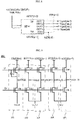
- FIG. 2 is a block diagram showing the configuration of a gate driver according to the present invention
- FIG. 3 is a block diagram showing the configuration of a GIP of FIG. 2 according to the present invention.
- the gate driver 2 includes a plurality of GIPs connected in cascade, and one GIP includes an output unit connected to two gate lines GL to sequentially generate two scan signals Vgout(n) and Vgout(n+1) and a carry signal COUT(n) according to clock signals SCCLKs and CRCLKs received from the timing controller 4.
- a plurality of clock signals SCCLKs and CRCLKs, a gate high voltage VGH, a plurality of gate low voltages VGLs and a gate start pulse VST received from the timing controller 4 are applied to the gate driver 2.
- the plurality of clock signals SCCLKs and CRCLKs includes scan pulse output clock signals SCCLKs and carry pulse output clock signals CRCLKs.
- Two gate driving signals Vgout(n) and Vgout(n+1) output from each GIP are used to sequentially drive the corresponding gate lines and the carry signal COUT(n) output from each GIP is used to reset a GIP of a previous stage or to set a GIP of a next stage.
- an n-th GIP is set by the carry signal COUT(n-3) output from a third previous stage and is reset by the carry signal COUT(n+3) output from a third next stage.
- the present invention is not limited thereto and various methods such as a method of setting an n-th GIP by the carry signal COUT(n-4) output from an (n-4)-th previous stage and resetting the n-th GIP by the carry signal COUT(n+4) output from an (n+4)-th next stage may be used. As shown in FIG.
- each GIP includes a node controller 100 set by the carry signal COUT output from the GIP of the previous stage and reset by the carry signal COUT output from the GIP of the next stage to control voltages of the first and second nodes Q and Qb, and an output unit 200 for receiving two of the plurality of scan pulse output clock signals SCCLKs and one of the plurality of carry pulse output clock signals CRCLKs and outputting at least two scan signals Vgout(n) and Vgout(n+1) and the carry signal COUT(n) according to the voltage levels of the first and second nodes Q and Qb.
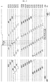
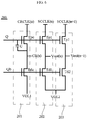
- FIG. 4 is a circuit diagram of the output unit 200 according to a first embodiment of the present invention
- FIG. 5 is a waveform diagram of the plurality of clock signals SCCLKs and CRCLKs applied to the output unit 200 and the voltage of a first node Q according to the first embodiment of the present invention shown in FIG. 4 .
- the output unit 200 of the GIP includes a carry signal output unit 201, a first scan signal output unit 202 and a second scan signal output unit 203, as shown in FIG. 4 .
- the carry signal output unit 201 includes a first pull-up transistor Tpc and a first pull-down transistor Tdc connected in series between a carry pulse output clock signal terminal CRCLK(n), to which one of the plurality of carry pulse output clock signal CRCLKs is applied, and a first gate low voltage terminal VGL1.
- the first pull-up transistor Tpc is turned on/off according to the voltage level of the first node Q and the first pull-down transistor Tdc is turned on/off according to the voltage level of the second node Qb, thereby outputting a carry signal CR(n).
- the first scan signal output unit 202 includes a second pull-up transistor Tp1, a second pull-down transistor Td1 and a first boosting capacitor C1.
- the second pull-up transistor Tp1 and the second pull-down transistor Td1 are connected in series between a scan pulse output clock signal terminal SCCLK(n), to which one of the plurality of scan pulse output clock signals SCCLKs is applied, and a second gate low voltage terminal VGL2.
- the first boosting capacitor C1 is connected between gate and source electrodes of the second pull-up transistor Tp1.
- the second pull-up transistor Tp1 is turned on/off according to the voltage level of the first node Q and the second pull-down transistor Td1 is turned on/off according to the voltage level of the second node Qb, thereby outputting a first scan signal Vout(n).
- the second scan signal output unit 203 includes a third pull-up transistor Tp2, and a third pull-down transistor Td2 and a second boosting capacitor C2.
- the third pull-up transistor Tp2 and the third pull-down transistor Td2 are connected in series between a 26an pulse output clock signal terminal SCCLK(n+1), to which another of the plurality of scan pulse output clock signals SCCLKs is applied, and the second gate low voltage terminal VGL2.
- the second boosting capacitor C2 is connected between gate and source electrodes of the third pull-up transistor Tp2.
- the third pull-up transistor Tp2 is turned on/off according to the voltage level of the first node Q and the third pull-down transistor Td2 is turned on/off according to the voltage level of the second node Qb, thereby outputting a second scan signal Vout(n+1).
- the channel width of the pull-up transistor Tpc of the carry signal output unit 201 is less than those of the pull-up transistors Tp1 and Tp2 of the first and second scan signal output units 202 and 203.
- the plurality of clock signals SCCLKs and CRCLKs includes the scan pulse output clock signals SCCLKs and the carry pulse output clock signals CRCLKs.
- the plurality of scan pulse output clock signals SCCLKs may include 12-phase clock signals shifted by a predetermined period, that is, first to twelfth clock signals SCCLK1 to SCCLK12.
- Each of the plurality of scan pulse output clock signals SCCLKs may have a high period during two horizontal periods (2H) and adjacent scan pulse output clock signals SCCLKs overlap each other during one horizontal period (1H).
- the carry pulse output clock signals CRCLKs may include 6-phase clock signals shifted by a predetermined period, that is, first to sixth clock signals CRCLK1 to CRCLK6.
- Each of the plurality of carry pulse output clock signals CRCLKs may have a high period during two horizontal periods (2H) and adjacent carry pulse output clock signals CRCLKs overlap each other during one horizontal period (1H).
- a third carry pulse output clock signal CRCLK3 is applied to the carry pulse output clock signal terminal CRCLK(n) of the carry signal output unit 201 of the GIP shown in FIG. 4
- a fifth scan pulse output clock signal SCCLK5 is applied to the scan pulse output clock signal terminal SCCLK(n) of the first scan signal output unit 202
- a sixth scan pulse output clock signal SCCLK6 is applied to the scan pulse output clock signal terminal SCCLK(n+1) of the second scan signal output unit 203.
- the node controller 100 of the GIP (n) shown in FIG. 3 is set by the carry signal COUT (the carry signal output from GIP(n-3) for outputting the carry pulse by CRCLK6 because GIP (n) outputs the carry pulse by a third carry pulse output clock signal CRCLK3) output from a GIP GIP(n-3) of a third previous stage and is reset by the carry signal COUT (CRCLK5) output from a GIP GIP(n+2) of a second next stage, thereby controlling the voltages of the first and second nodes Q and Qb.
- the carry signal COUT the carry signal output from GIP(n-3) for outputting the carry pulse by CRCLK6 because GIP (n) outputs the carry pulse by a third carry pulse output clock signal CRCLK3) output from a GIP GIP(n-3) of a third previous stage and is reset by the carry signal COUT (CRCLK5) output from a GIP GIP(n+2) of a second next stage, thereby controlling the voltages of the first
- the flat panel display device according to the first embodiment of the present invention since one GIP drives two gate lines, even when the flat panel display device is implemented with high resolution, it is possible to realize a flat panel display device having a narrow bezel.
- the output unit 200 of the GIP uses a method of boosting the first node Q using the scan signal.
- the boosting capacitance of the carry signal output unit 201 is less than those of the first and second scan signal output units 202 and 203, influence on the first node Q is low and the first and second capacitors C1 and C2 formed in the first and second scan signal output units 202 and 203 function as holding capacitors. Therefore, a boosting level deviation (difference between h1 and h2) of the first node Q occurs over time. To this end, a deviation occurs in the rising and falling times of the scan signals output from the first and second scan signal output units 202 and 203, thereby causing a periodic luminance deviation in an image displayed on the flat panel display device.
- Coupling between the outputs of the first and second scan signal output units 202 and 203 occurs to generate signal distortion.
- the voltage of the first node Q is partially decreased to decrease the gate-source voltage Vgs of each transistor of the output unit. Therefore, characteristics and reliability of the GIP may be reduced.
- FIG. 6 is a circuit diagram of an output unit 200 according to a second embodiment of the present invention
- FIG. 7 is a waveform diagram of a plurality of clock signals SCCLKs and CRCLKs applied to the output unit 200 according to the second embodiment of the present invention shown in FIG. 6 and the voltage of a first node Q.
- the output unit 200 of the GIP according to the second embodiment of the present invention includes a carry signal output unit 201, a first scan signal output unit 202 and a second scan signal output unit 203, as shown in FIG. 6 .
- the carry signal output unit 201 includes a first pull-up transistor Tpc, a first pull-down transistor Tdc and a boosting capacitor C.
- the first pull-up transistor Tpc and the first pull-down transistor Tdc are connected in series between a carry pulse output clock signal terminal CRCLK(n), to which one of the plurality of carry pulse output clock signals CRCLKs is applied, and a first gate low voltage terminal VGL1.
- the boosting capacitor C is connected between gate and source electrodes of the first pull-up transistor Tpc.
- the first pull-up transistor Tpc is turned on/off according to the voltage level of the first node Q and the first pull-down transistor Tdc is turned on/off according to the voltage level of the second node Qb, thereby outputting a carry signal CR(n).
- the first scan signal output 202 includes a second pull-up transistor Tp1 and a second pull-down transistor Td1 connected in series between a scan pulse output clock signal terminal SCCLK(n), to which one of the plurality of scan pulse output clock signals SCCLKs is applied, and a second gate low voltage terminal VGL2.
- the second pull-up transistor Tp1 is turned on/off according to the voltage level of the first node Q and the second pull-down transistor Td1 is turned on/off according to the voltage level of the second node Qb, thereby outputting a first scan signal Vout(n).
- the second scan signal output unit 203 includes a third pull-up transistor Tp2 and a third pull-down transistor Td2 connected in series between a scan pulse output clock signal terminal SCCLK(n+1), to which another of the plurality of scan pulse output clock signals SCCLKs is applied, and the second gate low voltage terminal VGL2.
- the third pull-up transistor Tp2 is turned on/off according to the voltage level of the first node Q and the third pull-down transistor Td2 is turned on/off according to the voltage level of the second node Qb, thereby outputting a second scan signal Vout (n+1) .
- the plurality of clock signals SCCLKs and CRCLKs includes the scan pulse output clock signals SCCLKs and the carry pulse output clock signals CRCLKs.
- the plurality of scan pulse output clock signals SCCLKs may include 12-phase clock signals shifted by a predetermined period, that is, first to twelfth clock signals SCCLK1 to SCCLK12.
- Each of the plurality of scan pulse output clock signals SCCLKs may have a high period during two horizontal periods (2H) and adjacent scan pulse output clock signals SCCLKs overlap each other during one horizontal period (1H).
- the carry pulse output clock signals CRCLKs may include 6-phase clock signals shifted by a predetermined period, that is, first to sixth clock signals CRCLK1 to CRCLK6.
- Each of the plurality of carry pulse output clock signals CRCLKs may have a high period during 3.5 horizontal periods (3.5H) and adjacent carry pulse output clock signals CRCLKs overlap each other during 1.5 horizontal periods (1.5H).
- each of the plurality of carry pulse output clock signals CRCLKs may have a high period during 3.5 horizontal periods (3.5H) and adjacent carry pulse output clock signals CRCLKs overlap each other during 1.5 horizontal periods (1.5H), on the assumption that each of the plurality of scan pulse output clock signals SCCLKs has a high period during two horizontal periods (2H) and adjacent scan pulse output clock signals SCCLKs overlap each other during one horizontal period (1H).
- each of the plurality of carry pulse output clock signals CRCLKs may have a longer high period than the high period (3H) of two adjacent scan pulse output clock signals SCCLKs, and adjacent carry pulse output clock signals CRCLKs overlap each other during a period longer than one horizontal period (1H).
- a third carry pulse output clock signal CRCLK3 is applied to the carry pulse output clock signal terminal CRCLK(n) of the carry signal output unit 201 of the GIP shown in FIG. 6
- a fifth scan pulse output clock signal SCCLK5 is applied to the scan pulse output clock signal terminal SCCLK(n) of the first scan signal output unit 202
- a sixth scan pulse output clock signal SCCLK6 is applied to the scan pulse output clock signal terminal SCCLK(n+1) of the second scan signal output unit 203.
- the node controller 100 of the GIP (n) shown in FIG. 3 is set by the carry signal COUT (the carry signal output from GIP(n-3) for outputting the carry pulse by CRCLK6 because GIP (n) outputs the carry pulse by a third carry pulse output clock signal CRCLK3) output from a GIP GIP(n-3) of a third previous stage and is reset by the carry signal COUT (CRCLK6) output from a GIP GIP(n+3) of a third next stage, thereby controlling the voltages of the first and second nodes Q and Qb.
- the carry signal COUT the carry signal output from GIP(n-3) for outputting the carry pulse by CRCLK6 because GIP (n) outputs the carry pulse by a third carry pulse output clock signal CRCLK3) output from a GIP GIP(n-3) of a third previous stage and is reset by the carry signal COUT (CRCLK6) output from a GIP GIP(n+3) of a third next stage, thereby controlling the voltages of the first
- one carry signal output unit and two scan signal output units are included such that one GIP drives two gate lines in the first and second embodiments of the present invention
- the present invention is not limited thereto and two or more scan signal output units may be included.
- FIG. 8 is a diagram illustrating an n-th GIP in a gate driver according to another embodiment of the present invention.
- the gate driver 2 includes the plurality of GIPs connected in cascade.
- One GIP includes the output connected to four gate lines GL to sequentially generate four scan signals Vgout(4n-3), Vgout(4n-2), Vgout(4n-1) and Vgout(4n) and the carry signal COUT(n) according to the clock signals SCCLKs and CRCLKs received from the timing controller 4.
- the n-th GIP(n) is set by the carry signal COUT(n-2) output from a second previous stage and is reset by the carry signal COUT(n+2) output from a second next stage.
- the present invention is not limited thereto.
- FIG. 9 is a circuit diagram of an output unit 200 according to a third embodiment of the present invention
- FIG. 10 is a waveform diagram of a plurality of clock signals SCCLKs and CRCLKs applied to the output unit 200 shown in FIG. 9 and the voltage of a first node Q.
- the output unit 200 of the GIP includes a carry signal output unit 201, a first scan signal output unit 202, a second scan signal output unit 203, a third scan signal output unit 204 and a fourth scan signal output unit 205, as shown in FIG. 9 .
- the carry signal output unit 201 includes a first pull-up transistor Tpc, a first pull-down transistor Tdc and a boosting capacitor C.
- the first pull-up transistor Tpc and the first pull-down transistor Tdc are connected in series between a carry pulse output clock signal terminal CRCLK(n), to which one of the plurality of carry pulse output clock signals CRCLKs is applied, and a first gate low voltage terminal VGL1.
- the boosting capacitor C is connected between the gate and source electrodes of the first pull-up transistor Tpc.
- the first pull-up transistor Tpc is turned on/off according to the voltage level of the first node Q and the first pull-down transistor Tdc is turned on/off according to the voltage level of the second node Qb, thereby outputting a carry signal CR(n).
- the first scan signal output unit 202 includes a second pull-up transistor Tp1 and a second pull-down transistor Td1 connected in series between a scan pulse output clock signal terminal SCCLK(n), to which one of the plurality of scan pulse output clock signals SCCLKs is applied, and a second gate low voltage terminal VGL2.
- the second pull-up transistor Tp1 is turned on/off according to the voltage level of the first node Q and the second pull-down transistor Td1 is turned on/off according to the voltage level of the second node Qb, thereby outputting a first scan signal Vout(n).
- the second scan signal output unit 203 includes a third pull-up transistor Tp2 and a third pull-down transistor Td2 connected in series between a scan pulse output clock signal terminal SCCLK(n+1), to which another of the plurality of scan pulse output clock signals SCCLKs is applied, and the second gate low voltage terminal VGL2.
- the third pull-up transistor Tp2 is turned on/off according to the voltage level of the first node Q and the third pull-down transistor Td2 is turned on/off according to the voltage level of the second node Qb, thereby outputting a second scan signal Vout (n+1) .
- the third scan signal output unit 204 includes a third pull-up transistor Tp3 and a third pull-down transistor Td3 connected in series between a scan pulse output clock signal terminal SCCLK(n+2), to which one of the plurality of scan pulse output clock signals SCCLKs is applied, and the second gate low voltage terminal VGL2.
- the third pull-up transistor Tp2 is turned on/off according to the voltage level of the first node Q and the third pull-down transistor Td2 is turned on/off according to the voltage level of the second node Qb, thereby outputting a third scan signal Vout (n+2) .
- the fourth scan signal output unit 205 includes a fourth pull-up transistor Tp4 and a fourth pull-down transistor Td4 connected in series between a scan pulse output clock signal terminal SCCLK(n+3), to which another of the plurality of scan pulse output clock signals SCCLKs is applied, and the second gate low voltage terminal VGL2.
- the fourth pull-up transistor Tp3 is turned on/off according to the voltage level of the first node Q and the fourth pull-down transistor Td3 is turned on/off according to the voltage level of the second node Qb, thereby outputting a fourth scan signal Vout(n+3).
- the plurality of clock signals SCCLKs and CRCLKs includes the scan pulse output clock signals SCCLKs and the carry pulse output clock signals CRCLKs.
- the plurality of scan pulse output clock signals SCCLKs may include 16-phase clock signals shifted by a predetermined period, that is, first to sixteenth clock signals SCCLK1 to SCCLK16.
- Each of the plurality of scan pulse output clock signals SCCLKs may have a high period during two horizontal periods (2H) and adjacent scan pulse output clock signals SCCLKs overlap each other during one horizontal period (1H).
- the carry pulse output clock signals CRCLKs may include 4-phase clock signals shifted by a predetermined period, that is, first to fourth clock signals CRCLK1 to CRCLK4.
- Each of the plurality of carry pulse output clock signals CRCLKs may have a high period during six horizontal periods (6H) and adjacent carry pulse output clock signals CRCLKs overlap each other during two horizontal periods (2H).
- each of the plurality of carry pulse output clock signals CRCLKs may have a high period during six horizontal periods (6H) and adjacent carry pulse output clock signals CRCLKs overlap each other during two horizontal periods (2H), on the assumption that each of the plurality of scan pulse output clock signals SCCLKs has a high period during two horizontal periods (2H) and adjacent scan pulse output clock signals SCCLKs overlap each other during one horizontal period (1H).
- each of the plurality of carry pulse output clock signals CRCLKs may have a longer high period than the high period (5H) of four adjacent scan pulse output clock signals SCCLKs, and adjacent carry pulse output clock signals CRCLKs overlap each other during a period longer than one horizontal period (1H).
- a third carry pulse output clock signal CRCLK3 is applied to the carry pulse output clock signal terminal CRCLK(n) of the carry signal output unit 201 of the GIP shown in FIG. 9
- a ninth scan pulse output clock signal SCCLK9 is applied to the scan pulse output clock signal terminal SCCLK(n) of the first scan signal output unit 202
- a tenth scan pulse output clock signal SCCLK10 is applied to the scan pulse output clock signal terminal SCCLK(n+1) of the second scan signal output unit 203
- an eleventh scan pulse output clock signal SCCLK11 is applied to the scan pulse output clock signal terminal SCCLK(n+2) of the third scan signal output unit 204
- a twelfth scan pulse output clock signal SCCLK12 is applied to the scan pulse output clock signal terminal SCCLK(n+3) of the fourth scan signal output unit 205.
- the node controller 100 of the GIP(n) shown in FIG. 3 is set by the carry signal CRCLK1 output from a GIP GIP(n-2) of a second previous stage and is reset by the carry signal CRCLK1 output from a GIP GIP(n+2) of a second next stage, thereby controlling the voltages of the first and second nodes Q and Qb.
- the number of scan pulse output clock signals SCCLKs, the number of carry pulse output clock signals CRCLKs and the waveform of each clock signal may be variously changed.
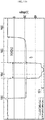
- FIG. 11a is a waveform diagram of the voltage of a first node Q and the carry signal output clock signal of the gate driver according to the first embodiment of the present invention
- FIG. 11b is a waveform of the voltage of the first node Q and the carry signal output clock signal of a gate driver according to the second and third embodiments of the present invention.
- FIG. 12a is an output waveform diagram of scan signals of the gate driver according to the first embodiment of the present invention
- FIG. 12b is an output waveform diagram of scan signals of the gate driver according to the second and third embodiments of the present invention.
- the output unit 200 of the GIP uses a method of boosting the first node Q using the scan signal and the scan pulse output clock signal SCCLK(n) and the carry pulse output clock signal CRCLK(n) have the same width.
- the output unit 200 of the GIP uses a method of boosting the first node Q using the scan signal and the scan pulse output clock signal SCCLK(n) and the carry pulse output clock signal CRCLK(n) have the same width, a boosting level deviation (difference between h1 and h2) of the first node Q was about 14.8V.
- the output unit 200 of the GIP uses a method of boosting the first node Q using the carry signal and the width of the carry pulse output clock signal CRCLK(n) is greater than that of the scan pulse output clock signal SCCLK(n).
- the output unit 200 of the GIP uses a method of boosting the first node Q using the carry signal and the width of the carry pulse output clock signal CRCLK(n) is greater than that of the scan pulse output clock signal SCCLK(n), a boosting level deviation (difference between h1 and h2) of the first node Q was about 4.0V.
- the output unit 200 of the GIP according to the second and third embodiments of the present invention can reduce the boosting level deviation (difference between h1 and h2) of the first node Q as compared to the output unit 200 according to the first embodiment of the present invention.
- the output unit 200 according to the first embodiment of the present invention uses the method of boosting the first node Q using the scan signal
- the output unit 200 of the GIP according to the second and third embodiments of the present invention uses the method of boosting the first node Q using the carry signal. Accordingly, according to the second and third embodiments of the present invention, it is possible to reduce influence of the transistors of each scan signal output unit 202, 203, 204 or 205, as can be seen from comparison between FIGS. 12a and 12b .
- the output unit 200 of the GIP according to the second and third embodiments of the present invention can reduce influence of the transistors of the scan signal output units 202, 203, 204 and 205 and reduce the boosting level deviation (difference between h1 and h2) of the first node Q as compared to the output unit 200 of the GIP according to the first embodiment of the present invention, it is possible to reduce the deviation occurring in the rising and falling times of the scan signals output from the scan signal output units 202, 203, 204 and 205 and a periodic luminance deviation in the display displayed on the flat panel display panel.
- the output unit 200 of the GIP according to the second and third embodiments of the present invention sets the width of the carry pulse output clock signal CRCLK(n) to be greater than that of the scan pulse output clock signal SCCLK(n) to reduce the boosting level deviation (difference between h1 and h2) of the first node Q as compared to the output unit 200 of the GIP according to the first embodiment of the present invention, it is possible to maintain the boosting level of the first node Q at a high level while the scan pulse is output and to prevent characteristics and reliability of the GIP from being reduced due to decrease in gate-source voltage Vgs of each transistor of the output unit.
- the boosting capacitor is installed only in the carry signal output unit and the boosting level deviation (difference between h1 and h2) of the first node Q is reduced, even when at least two scan signal output units are included, coupling between the scan signal output units does not occur, thereby preventing signal distortion.
- the boosting capacitor C is installed only in the carry signal output unit 201, the capacity of the boosting capacitor is increased to secure the boosting level of the first node Q. Therefore, it is possible to secure output characteristics and positive bias temperature stress (PBTS) margin of the pull-up transistor of each output unit.
- PBTS positive bias temperature stress
- the gate driver and the flat panel display device according to the present invention having the above-described features have the following effects.
- the gate driver according to each embodiment of the present invention since one GIP drives at least two gate lines, even when the flat panel display device is implemented with high resolution, it is possible to realize a flat panel display device having a narrow bezel.
- the output unit of the GIP according to the second and third embodiments of the present invention uses the method of boosting the first node Q using the carry signal.
- the boosting capacitor is installed only in the carry signal output unit, it is possible to reduce influence of the transistor of each scan signal output unit and to reduce the boosting level deviation of the first node. Therefore, it is possible to reduce the deviation occurring in the rising and falling times of the scan signals output from each scan signal output unit and a periodic luminance deviation in the display displayed on the flat panel display panel.
- the boosting level deviation of the first node is reduced and the width of the carry signal output clock signal is increased to maintain the boosting level of the first node at a high level while the scan pulse is output, it is possible to prevent characteristics and reliability of the GIP from being reduced due to decrease in gate-source voltage Vgs of each transistor of the output unit.
- the boosting capacitor Since the boosting capacitor is installed only in the carry signal output unit, the capacity of the boosting capacitor is increased, thereby securing the boosting level of the first node. Therefore, it is possible to secure output characteristics and positive bias temperature stress (PBTS) margin of the pull-up transistor of each output unit.
- PBTS positive bias temperature stress
- a gate driver comprising: a plurality of gate-in-panels GIP for sequentially supplying scan signals to a plurality of gate lines; wherein each GIP comprises a carry signal output unit and at least two scan signal output units to drive at least two gate lines, and wherein the carry signal output unit comprises a pull-up transistor controlled by a voltage of a first node, a pull-down transistor controlled by a voltage of a second node, and a boosting capacitor formed between gate and source electrodes of the pull-up transistor.
- one of a plurality of scan pulse output clock signals is applied to each of the at least two scan signal output units, and one of a plurality of carry pulse output clock signals is applied to the carry signal output unit, wherein the plurality of scan pulse output clock signals are shifted by a predetermined period, each scan pulse output clock signal has a high period during a predetermined horizontal period and adjacent scan pulse output clock signals overlap each other during a predetermined period, and wherein the plurality of carry pulse output clock signals are shifted by a predetermined period, each carry pulse output clock signal has a longer high period than a high period of two adjacent scan pulse output clock signals, and adjacent carry pulse output clock signals overlap each other during a period longer than one horizontal period.
- the at least two scan signal output units comprise first and second scan signal output units to drive two gate lines, wherein one of a plurality of scan pulse output clock signals is applied to the first scan signal output unit, wherein another of the plurality of scan pulse output clock signals is applied to the second scan signal output unit, wherein one of a plurality of carry pulse output clock signals is applied to the carry signal output unit, wherein the plurality of scan pulse output clock signals are shifted by a predetermined period, each scan pulse output clock signal has a high period during a predetermined period and adjacent scan pulse output clock signals overlap each other during a predetermined period, and wherein the plurality of carry pulse output clock signals are shifted by a predetermined period, each carry pulse output clock signal has a longer high period than a high period of two adjacent scan pulse output clock signals, and adjacent carry pulse output clock signals overlap each other during a period longer than one horizontal period.
- each scan pulse output clock signal has a high period during two horizontal periods and adjacent scan pulse output clock signals overlap each other during one horizontal period
- each carry pulse output clock signal has a high period during 3.5 horizontal periods and adjacent carry pulse output clock signals overlap each other during 1.5 horizontal periods.
- the at least two scan signal output units comprise first to fourth scan signal output units to drive four gate lines.
- one of a plurality of scan pulse output clock signals is applied to each of the first to fourth scan signal output units, another of the plurality of scan pulse output clock signals is applied to the second scan signal output unit, still another of the plurality of scan pulse output clock signals is applied to the third scan signal output unit, yet another of the plurality of scan pulse output clock signals is applied to the fourth scan signal output unit, and one of a plurality of carry pulse output clock signals is applied to the carry signal output unit, wherein the plurality of scan pulse output clock signals are shifted by a predetermined period, each scan pulse output clock signal has a high period during a predetermined horizontal period and adjacent scan pulse output clock signals overlap each other during a predetermined period, and wherein the plurality of carry pulse output clock signals are shifted by a predetermined period, each carry pulse output clock signal has a longer high period than a high period of four adjacent scan pulse output clock signals, and adjacent carry pulse output clock signals overlap each other during a period longer than one horizontal period.
- each scan pulse output clock signal has a high period during two horizontal periods and adjacent scan pulse output clock signals overlap each other during one horizontal period
- each carry pulse output clock signal has a high period during six horizontal periods and adjacent carry pulse output clock signals overlap each other during two horizontal periods.
- a flat panel display device comprising: a display panel including a plurality of gate lines and a plurality of data lines and a plurality of subpixels formed in a matrix to supply data voltages to the plurality of data lines in response to scan pulses supplied to the plurality of gate lines to display an image; a gate driver according to one or more embodiments described herein for sequentially supplying the scan pulses to the plurality of gate lines; a data driver for supplying the data voltages to the plurality of data lines; and a timing controller for aligning image data received from the outside according to a size and resolution of the display panel to supply the image data to the data driver and respectively supplying a plurality of gate control signals and a plurality of data control signals to the gate driver and the data driver using synchronization signals received from the outside.
- a gate driver comprising: a plurality of gate-in-panels GIP for sequentially supplying scan signals to a plurality of gate lines; wherein each GIP comprises a carry signal output unit and first and second scan signal output units to drive at least two gate lines, and wherein the carry signal output unit comprises a pull-up transistor controlled by a voltage of a first node, a pull-down transistor controlled by a voltage of a second node, and a boosting capacitor formed between gate and source electrodes of the pull-up transistor.
- one of a plurality of scan pulse output clock signals is applied to the first scan signal output unit, another of the plurality of scan pulse output clock signals is applied to the second scan signal output unit, and one of a plurality of carry pulse output clock signals is applied to the carry signal output unit, wherein the plurality of scan pulse output clock signals are shifted by a predetermined period, each scan pulse output clock signal has a high period during a predetermined period and adjacent scan pulse output clock signals overlap each other during a predetermined period, and wherein the plurality of carry pulse output clock signals are shifted by a predetermined period, each carry pulse output clock signal has a longer high period than a high period of two adjacent scan pulse output clock signals, and adjacent carry pulse output clock signals overlap each other during a period longer than one horizontal period.
- each scan pulse output clock signal has a high period during two horizontal periods and adjacent scan pulse output clock signals overlap each other during one horizontal period, wherein each carry pulse output clock signal has a high period during 3.5 horizontal periods and adjacent carry pulse output clock signals overlap each other during 1.5 horizontal periods.
- a gate driver comprising: a plurality of gate-in-panels GIP for sequentially supplying scan signals to a plurality of gate lines; wherein each GIP comprises a carry signal output unit and first to fourth scan signal output units to drive at least four gate lines, and wherein the carry signal output unit comprises a pull-up transistor controlled by a voltage of a first node, a pull-down transistor controlled by a voltage of a second node, and a boosting capacitor formed between gate and source electrodes of the pull-up transistor.
- one of a plurality of scan pulse output clock signals is applied to each of the first to fourth scan signal output units, and one of a plurality of carry pulse output clock signals is applied to the carry signal output unit, wherein the plurality of scan pulse output clock signals are shifted by a predetermined period, each scan pulse output clock signal has a high period during a predetermined horizontal period and adjacent scan pulse output clock signals overlap each other during a predetermined period, and wherein the plurality of carry pulse output clock signals are shifted by a predetermined period, each carry pulse output clock signal has a longer high period than a high period of four adjacent scan pulse output clock signals, and adjacent carry pulse output clock signals overlap each other during a period longer than one horizontal period.
- each scan pulse output clock signal has a high period during two horizontal periods and adjacent scan pulse output clock signals overlap each other during one horizontal period
- each carry pulse output clock signal has a high period during six horizontal periods and adjacent carry pulse output clock signals overlap each other during two horizontal periods.
- a flat panel display device comprising: a display panel including a plurality of gate lines and a plurality of data lines and a plurality of subpixels formed in a matrix to supply data voltages to the plurality of data lines in response to scan pulses supplied to the plurality of gate lines to display an image; a gate driver for sequentially supplying the scan pulses to the plurality of gate lines; a data driver for supplying the data voltages to the plurality of data lines; and a timing controller for aligning image data received from the outside according to a size and resolution of the display panel to supply the image data to the data driver and respectively supplying a plurality of gate control signals and a plurality of data control signals to the gate driver and the data driver using synchronization signals received from the outside, wherein the gate driver comprises a plurality of gate-in-panels GIP for sequentially supplying scan signals to the plurality of gate lines, wherein each GIP comprises one carry signal output unit and at least two scan signal output units to drive at least two gate lines, and where
- the at least two scan signal output units comprise first and second scan signal output units to drive two gate lines, and one of a plurality of scan pulse output clock signals is applied to each of the at least two scan signal output units, wherein one of a plurality of carry pulse output clock signals is applied to the carry signal output unit, wherein the plurality of scan pulse output clock signals are shifted by a predetermined period, each scan pulse output clock signal has a high period during a predetermined period and adjacent scan pulse output clock signals overlap each other during a predetermined period, and wherein the plurality of carry pulse output clock signals are shifted by a predetermined period, each carry pulse output clock signal has a longer high period than a high period of two adjacent scan pulse output clock signals, and adjacent carry pulse output clock signals overlap each other during a period longer than one horizontal period.
- the at least two scan signal output units comprise first to fourth scan signal output units to drive four gate lines and one of a plurality of scan pulse output clock signals is applied to each of the first to fourth scan signal output units, wherein one of a plurality of carry pulse output clock signals is applied to the carry signal output unit, wherein the plurality of scan pulse output clock signals are shifted by a predetermined period, each scan pulse output clock signal has a high period during a predetermined horizontal period and adjacent scan pulse output clock signals overlap each other during a predetermined period, and wherein the plurality of carry pulse output clock signals are shifted by a predetermined period, each carry pulse output clock signal has a longer high period than a high period of four adjacent scan pulse output clock signals, and adjacent carry pulse output clock signals overlap each other during a period longer than one horizontal period.
Landscapes
- Engineering & Computer Science (AREA)
- Physics & Mathematics (AREA)
- Computer Hardware Design (AREA)
- General Physics & Mathematics (AREA)
- Theoretical Computer Science (AREA)
- Chemical & Material Sciences (AREA)
- Crystallography & Structural Chemistry (AREA)
- Control Of Indicators Other Than Cathode Ray Tubes (AREA)
- Liquid Crystal Display Device Control (AREA)
- Control Of El Displays (AREA)
- Electronic Switches (AREA)
- Shift Register Type Memory (AREA)
Abstract
Description
- This application claims the benefit of Korean Patent Application No.
10-2017-0098872, filed on August 04, 2017 - The present invention relates to a gate driver of a display device and, more particularly, to a gate driver for outputting a plurality of scan pulses in one gate-in-panel (GIP) and a flat panel display device including the same.
- With development of information-oriented society and development of various portable electronic apparatuses such as mobile communication terminals and laptops, demand for flat panel display devices has gradually increased.
- As a flat panel display device, a liquid crystal display (LCD) device using liquid crystal and an organic light emitting diode (OLED) display device using an OLED are used.
- Such a flat panel display device includes a display panel including a plurality of gate lines and a plurality of data lines to display an image, and a driver for driving the display panel.
- The driver includes a gate driver for driving the plurality of gate lines, a data driver for driving the plurality of data lines, and a timing controller for supplying image data and various control signals to the gate driver and the data driver.
- The gate driver may be simultaneously formed in a non-active area of the display panel in a process of forming the plurality of gate lines and the plurality of data lines of the display panel and pixels.
- That is, a gate-in-panel (hereinafter referred to as GIP) method of integrating the gate driver on the display panel is applied. In addition, GIPs are configured to correspond one-to-one to the plurality of gate lines.
- However, with high resolution and narrow bezel of the flat panel display device, one GIP needs to drive two or more gate lines.
- Accordingly, the present invention is directed to a gate driver and a flat panel display device including the same that substantially obviate one or more problems due to limitations and disadvantages of the related art.
- An object of the present invention is to provide a gate driver including at least two output buffers to drive at least two gate lines and capable of reducing an output deviation of each output buffer, and a flat panel display device including the same.
- Additional advantages, objects, and features of the invention will be set forth in part in the description which follows and in part will become apparent to those having ordinary skill in the art upon examination of the following or may be learned from practice of the invention. The objectives and other advantages of the invention may be realized and attained by the structure particularly pointed out in the written description and claims hereof as well as the appended drawings.
- To achieve these objects and other advantages and in accordance with the purpose of the invention, as embodied and broadly described herein, there is provided a gate driver according to
claim 1. Further embodiments are described in the dependent claims. According to an aspect of the present invention, a gate driver includes a plurality of gate-in-panels (GIPs) for sequentially supplying scan signals to a plurality of gate lines. Each GIP includes one carry signal output unit and at least two scan signal output units to drive at least two gate lines, and the carry signal output unit includes a pull-up transistor controlled by a voltage of a first node, a pull-down transistor controlled by a voltage of a second node, and a boosting capacitor formed between gate and source electrodes of the pull-up transistor. - The at least two scan signal output units may include first and second scan signal output units to drive two gate lines, one of a plurality of scan pulse output clock signals may be applied to each of the at least two scan signal output units, one of a plurality of carry pulse output clock signals may be applied to the carry signal output unit, the plurality of carry pulse output clock signals may be shifted by a predetermined period, adjacent scan pulse output clock signals overlap each other during a predetermined period, and each carry pulse output clock signal may have a longer high period than a high period of two adjacent scan pulse output clock signals, and adjacent carry pulse output clock signals may overlap each other during a period longer than one horizontal period.
- Each scan pulse output clock signal may have a high period during two horizontal periods and adjacent scan pulse output clock signals may overlap each other during one horizontal period, and each carry pulse output clock signal may have a high period during 3.5 horizontal periods and adjacent carry pulse output clock signals may overlap each other during 1.5 horizontal periods.
- The at least two scan signal output units may include first to fourth scan signal output units to drive four gate lines, one of a plurality of scan pulse output clock signals may be applied to each of the first to fourth scan signal output units, one of a plurality of carry pulse output clock signals may be applied to the carry signal output unit, the plurality of carry pulse output clock signals may be shifted by a predetermined period, adjacent scan pulse output clock signals overlap each other during a predetermined period, and each carry pulse output clock signal may have a longer high period than a high period of four adjacent scan pulse output clock signals, and adjacent carry pulse output clock signals may overlap each other during a period longer than one horizontal period.
- Each scan pulse output clock signal may have a high period during two horizontal periods and adjacent scan pulse output clock signals may overlap each other during one horizontal period. Each carry pulse output clock signal may have a high period during six horizontal periods and adjacent carry pulse output clock signals may overlap each other during two horizontal periods.
- According to another aspect of the present invention, a flat panel display device includes a display panel including a plurality of gate lines and a plurality of data lines and a plurality of subpixels formed in a matrix to supply data voltages to the plurality of data lines in response to scan pulses supplied to the plurality of gate lines to display an image, a gate driver for sequentially supplying the scan pulses to the plurality of gate lines, a data driver for supplying the data voltages to the plurality of data lines, and a timing controller for aligning image data received from the outside according to a size and resolution of the display panel to supply the image data to the data driver and respectively supplying a plurality of gate control signals and a plurality of data control signals to the gate driver and the data driver using signals received from the outside. The gate driver includes a plurality of gate-in-panels (GIPs) for sequentially supplying scan signals to the plurality of gate lines, each GIP comprises one carry signal output unit and at least two scan signal output units to drive at least two gate lines, and the carry signal output unit includes a pull-up transistor controlled by a voltage of a first node, a pull-down transistor controlled by a voltage of a second node, and a boosting capacitor formed between gate and source electrodes of the pull-up transistor.
- It is to be understood that both the foregoing general description and the following detailed description of the present invention are exemplary and explanatory and are intended to provide further explanation of the invention as claimed.
- The accompanying drawings, which are included to provide a further understanding of the invention and are incorporated in and constitute a part of this application, illustrate embodiment(s) of the invention and together with the description serve to explain the principle of the invention. In the drawings:
-
FIG. 1 is a diagram schematically showing a flat panel display device according to the present invention; -
FIG. 2 is a block diagram showing the configuration of a gate driver according to the present invention; -
FIG. 3 is a block diagram showing the configuration of a GIP ofFIG. 2 according to the present invention; -
FIG. 4 is a circuit diagram of an output unit according to a first embodiment of the present invention; -
FIG. 5 is a waveform diagram of a plurality of clock signals SCCLKs and CRCLKs applied to the output unit according to the first embodiment of the present invention shown inFIG. 4 and the voltage of a first node Q; -
FIG. 6 is a circuit diagram of an output unit according to a second embodiment of the present invention; -
FIG. 7 is a waveform diagram of a plurality of clock signals SCCLKs and CRCLKs applied to the output unit according to the second embodiment of the present invention shown inFIG. 6 and the voltage of a first node Q; -
FIG. 8 is a diagram illustrating an n-th GIP in a gate driver according to another embodiment of the present invention; -
FIG. 9 is a circuit diagram of an output unit according to a third embodiment of the present invention; -
FIG. 10 is a waveform diagram of a plurality of clock signals SCCLKs and CRCLKs applied to the output unit shown inFIG. 9 and the voltage of a first node Q; -
FIG. 11a is a waveform diagram of the voltage of a first node Q and the carry signal output clock signal of the gate driver according to the first embodiment of the present invention andFIG. 11b is a waveform of the voltage of the first node Q and the carry signal output clock signal of a gate driver according to the second and third embodiments of the present invention; and -
FIG. 12a is an output waveform diagram of scan signals of the gate driver according to the first embodiment of the present invention, andFIG. 12b is an output waveform diagram of scan signals of the gate driver according to the second and third embodiments of the present invention. - The gate driver and the flat panel display device including the same according to the present invention having the above-described features will be described in greater detail with reference to the accompanying drawings.
-
FIG. 1 is a diagram schematically showing a flat panel display device according to the present invention. - As shown in
FIG. 1 , the flat panel display device according to the present invention includes adisplay panel 1, agate driver 2, adata driver 3 and atiming controller 4. - On the
display panel 1, a plurality of gate lines GL1∼GLn and a plurality of data lines DL1∼DLm are disposed and a plurality of subpixels P are arranged at intersections between the plurality of gate lines GL1∼GLn and the plurality of data lines DL1∼DLm in a matrix. The plurality of subpixels P display an image according to image signals (data voltages) received from the plurality of data lines DL1∼DLm in response to scan pulses received from the gate lines GL1∼GLn. - The
gate driver 2 is a gate-in-panel (GIP) type gate driver and is disposed in the non-active area of thedisplay panel 1. - The
gate driver 2 includes a gate shift register for sequentially supplying the scan pulse (gate driving signal) Vgout to each gate line GL1∼GLn according to a plurality of gate control signals GCS received from thetiming controller 4. - The plurality of gate control signals GCS includes a plurality of clock signals having different phases, a gate start signal VST indicating driving start of the
gate driver 2, a gate high voltage VGH and a gate low voltage VGL. - The
data driver 3 converts digital image data RGB received from thetiming controller 4 into an analog data voltage using a reference gamma voltage and supplies the converted analog data voltage to the plurality of data lines DL1∼DLm. Thedata driver 3 is controlled according to a plurality of data control signals DCS received from thetiming controller 4. - The
timing controller 4 aligns the image data RGB received from the outside according to the size and resolution of thedisplay panel 1 and supplies the image data to thedata driver 3. In addition, thetiming controller 4 generates a plurality of gate control signals GCS and a plurality of data control signals DCS using signals received from the outside, such as a dot clock, a data enable signal, a horizontal synchronization signal and a vertical synchronization signal and respectively supplies the gate control signals and the data control signals to thegate driver 2 and thedata driver 3. - The
gate driver 2 includes a plurality of stages (GIPs) in order to sequentially supply the scan pulse (gate driving signal) Vgout to each of the plurality of gate lines GL1∼GLn. - However, when the plurality of GIPs are connected to correspond one-to-one to the plurality of gate lines, recent design requirements such as high resolution and narrow bezel are not satisfied.
- Accordingly, one of the plurality of GIPs according to the present invention includes one carry signal output unit and at least two scan signal output units such that one GIP drives at least two gate lines.
-
FIG. 2 is a block diagram showing the configuration of a gate driver according to the present invention, andFIG. 3 is a block diagram showing the configuration of a GIP ofFIG. 2 according to the present invention. - As shown in
FIG. 2 , thegate driver 2 according to the present invention includes a plurality of GIPs connected in cascade, and one GIP includes an output unit connected to two gate lines GL to sequentially generate two scan signals Vgout(n) and Vgout(n+1) and a carry signal COUT(n) according to clock signals SCCLKs and CRCLKs received from thetiming controller 4. - Specifically, a plurality of clock signals SCCLKs and CRCLKs, a gate high voltage VGH, a plurality of gate low voltages VGLs and a gate start pulse VST received from the
timing controller 4 are applied to thegate driver 2. - The plurality of clock signals SCCLKs and CRCLKs includes scan pulse output clock signals SCCLKs and carry pulse output clock signals CRCLKs.
- Two gate driving signals Vgout(n) and Vgout(n+1) output from each GIP are used to sequentially drive the corresponding gate lines and the carry signal COUT(n) output from each GIP is used to reset a GIP of a previous stage or to set a GIP of a next stage.
- In
FIG. 2 , an n-th GIP is set by the carry signal COUT(n-3) output from a third previous stage and is reset by the carry signal COUT(n+3) output from a third next stage. However, the present invention is not limited thereto and various methods such as a method of setting an n-th GIP by the carry signal COUT(n-4) output from an (n-4)-th previous stage and resetting the n-th GIP by the carry signal COUT(n+4) output from an (n+4)-th next stage may be used. As shown inFIG. 3 , each GIP includes anode controller 100 set by the carry signal COUT output from the GIP of the previous stage and reset by the carry signal COUT output from the GIP of the next stage to control voltages of the first and second nodes Q and Qb, and anoutput unit 200 for receiving two of the plurality of scan pulse output clock signals SCCLKs and one of the plurality of carry pulse output clock signals CRCLKs and outputting at least two scan signals Vgout(n) and Vgout(n+1) and the carry signal COUT(n) according to the voltage levels of the first and second nodes Q and Qb. -
FIG. 4 is a circuit diagram of theoutput unit 200 according to a first embodiment of the present invention, andFIG. 5 is a waveform diagram of the plurality of clock signals SCCLKs and CRCLKs applied to theoutput unit 200 and the voltage of a first node Q according to the first embodiment of the present invention shown inFIG. 4 . - The
output unit 200 of the GIP according to the first embodiment of the present invention includes a carrysignal output unit 201, a first scansignal output unit 202 and a second scansignal output unit 203, as shown inFIG. 4 . - The carry
signal output unit 201 according to the first embodiment of the present invention includes a first pull-up transistor Tpc and a first pull-down transistor Tdc connected in series between a carry pulse output clock signal terminal CRCLK(n), to which one of the plurality of carry pulse output clock signal CRCLKs is applied, and a first gate low voltage terminal VGL1. The first pull-up transistor Tpc is turned on/off according to the voltage level of the first node Q and the first pull-down transistor Tdc is turned on/off according to the voltage level of the second node Qb, thereby outputting a carry signal CR(n). - The first scan
signal output unit 202 according to the first embodiment of the present invention includes a second pull-up transistor Tp1, a second pull-down transistor Td1 and a first boosting capacitor C1. The second pull-up transistor Tp1 and the second pull-down transistor Td1 are connected in series between a scan pulse output clock signal terminal SCCLK(n), to which one of the plurality of scan pulse output clock signals SCCLKs is applied, and a second gate low voltage terminal VGL2. The first boosting capacitor C1 is connected between gate and source electrodes of the second pull-up transistor Tp1. The second pull-up transistor Tp1 is turned on/off according to the voltage level of the first node Q and the second pull-down transistor Td1 is turned on/off according to the voltage level of the second node Qb, thereby outputting a first scan signal Vout(n). - The second scan
signal output unit 203 according to the first embodiment of the present invention includes a third pull-up transistor Tp2, and a third pull-down transistor Td2 and a second boosting capacitor C2. The third pull-up transistor Tp2 and the third pull-down transistor Td2 are connected in series between a 26an pulse output clock signal terminal SCCLK(n+1), to which another of the plurality of scan pulse output clock signals SCCLKs is applied, and the second gate low voltage terminal VGL2. The second boosting capacitor C2 is connected between gate and source electrodes of the third pull-up transistor Tp2. The third pull-up transistor Tp2 is turned on/off according to the voltage level of the first node Q and the third pull-down transistor Td2 is turned on/off according to the voltage level of the second node Qb, thereby outputting a second scan signal Vout(n+1). - The channel width of the pull-up transistor Tpc of the carry
signal output unit 201 is less than those of the pull-up transistors Tp1 and Tp2 of the first and second scansignal output units - As shown in
FIG. 5 , the plurality of clock signals SCCLKs and CRCLKs according to the first embodiment of the present invention includes the scan pulse output clock signals SCCLKs and the carry pulse output clock signals CRCLKs. - The plurality of scan pulse output clock signals SCCLKs may include 12-phase clock signals shifted by a predetermined period, that is, first to twelfth clock signals SCCLK1 to SCCLK12. Each of the plurality of scan pulse output clock signals SCCLKs may have a high period during two horizontal periods (2H) and adjacent scan pulse output clock signals SCCLKs overlap each other during one horizontal period (1H).
- The carry pulse output clock signals CRCLKs may include 6-phase clock signals shifted by a predetermined period, that is, first to sixth clock signals CRCLK1 to CRCLK6. Each of the plurality of carry pulse output clock signals CRCLKs may have a high period during two horizontal periods (2H) and adjacent carry pulse output clock signals CRCLKs overlap each other during one horizontal period (1H).
- In
FIG. 5 , a third carry pulse output clock signal CRCLK3 is applied to the carry pulse output clock signal terminal CRCLK(n) of the carrysignal output unit 201 of the GIP shown inFIG. 4 , a fifth scan pulse output clock signal SCCLK5 is applied to the scan pulse output clock signal terminal SCCLK(n) of the first scansignal output unit 202, and a sixth scan pulse output clock signal SCCLK6 is applied to the scan pulse output clock signal terminal SCCLK(n+1) of the second scansignal output unit 203. - In addition, in
FIG. 5 , thenode controller 100 of the GIP (n) shown inFIG. 3 is set by the carry signal COUT (the carry signal output from GIP(n-3) for outputting the carry pulse by CRCLK6 because GIP (n) outputs the carry pulse by a third carry pulse output clock signal CRCLK3) output from a GIP GIP(n-3) of a third previous stage and is reset by the carry signal COUT (CRCLK5) output from a GIP GIP(n+2) of a second next stage, thereby controlling the voltages of the first and second nodes Q and Qb. - As described with reference to
FIGs. 2 to 5 , in the flat panel display device according to the first embodiment of the present invention, since one GIP drives two gate lines, even when the flat panel display device is implemented with high resolution, it is possible to realize a flat panel display device having a narrow bezel. - However, the
output unit 200 of the GIP according to the first embodiment of the present invention uses a method of boosting the first node Q using the scan signal. - Accordingly, since the boosting capacitance of the carry
signal output unit 201 is less than those of the first and second scansignal output units signal output units signal output units - Coupling between the outputs of the first and second scan
signal output units - Accordingly, in order to solve the above problems, another embodiment of the present invention will be provided.
-
FIG. 6 is a circuit diagram of anoutput unit 200 according to a second embodiment of the present invention, andFIG. 7 is a waveform diagram of a plurality of clock signals SCCLKs and CRCLKs applied to theoutput unit 200 according to the second embodiment of the present invention shown inFIG. 6 and the voltage of a first node Q. - The
output unit 200 of the GIP according to the second embodiment of the present invention includes a carrysignal output unit 201, a first scansignal output unit 202 and a second scansignal output unit 203, as shown inFIG. 6 . - The carry
signal output unit 201 according to the second embodiment of the present invention includes a first pull-up transistor Tpc, a first pull-down transistor Tdc and a boosting capacitor C. The first pull-up transistor Tpc and the first pull-down transistor Tdc are connected in series between a carry pulse output clock signal terminal CRCLK(n), to which one of the plurality of carry pulse output clock signals CRCLKs is applied, and a first gate low voltage terminal VGL1. The boosting capacitor C is connected between gate and source electrodes of the first pull-up transistor Tpc. The first pull-up transistor Tpc is turned on/off according to the voltage level of the first node Q and the first pull-down transistor Tdc is turned on/off according to the voltage level of the second node Qb, thereby outputting a carry signal CR(n). - The first
scan signal output 202 according to the second embodiment of the present invention includes a second pull-up transistor Tp1 and a second pull-down transistor Td1 connected in series between a scan pulse output clock signal terminal SCCLK(n), to which one of the plurality of scan pulse output clock signals SCCLKs is applied, and a second gate low voltage terminal VGL2. The second pull-up transistor Tp1 is turned on/off according to the voltage level of the first node Q and the second pull-down transistor Td1 is turned on/off according to the voltage level of the second node Qb, thereby outputting a first scan signal Vout(n). - The second scan
signal output unit 203 according to the second embodiment of the present invention includes a third pull-up transistor Tp2 and a third pull-down transistor Td2 connected in series between a scan pulse output clock signal terminal SCCLK(n+1), to which another of the plurality of scan pulse output clock signals SCCLKs is applied, and the second gate low voltage terminal VGL2. The third pull-up transistor Tp2 is turned on/off according to the voltage level of the first node Q and the third pull-down transistor Td2 is turned on/off according to the voltage level of the second node Qb, thereby outputting a second scan signal Vout (n+1) . - As shown in
FIG. 7 , the plurality of clock signals SCCLKs and CRCLKs according to the second embodiment of the present invention includes the scan pulse output clock signals SCCLKs and the carry pulse output clock signals CRCLKs. - The plurality of scan pulse output clock signals SCCLKs may include 12-phase clock signals shifted by a predetermined period, that is, first to twelfth clock signals SCCLK1 to SCCLK12. Each of the plurality of scan pulse output clock signals SCCLKs may have a high period during two horizontal periods (2H) and adjacent scan pulse output clock signals SCCLKs overlap each other during one horizontal period (1H).
- The carry pulse output clock signals CRCLKs may include 6-phase clock signals shifted by a predetermined period, that is, first to sixth clock signals CRCLK1 to CRCLK6. Each of the plurality of carry pulse output clock signals CRCLKs may have a high period during 3.5 horizontal periods (3.5H) and adjacent carry pulse output clock signals CRCLKs overlap each other during 1.5 horizontal periods (1.5H).
- For convenience of description, each of the plurality of carry pulse output clock signals CRCLKs may have a high period during 3.5 horizontal periods (3.5H) and adjacent carry pulse output clock signals CRCLKs overlap each other during 1.5 horizontal periods (1.5H), on the assumption that each of the plurality of scan pulse output clock signals SCCLKs has a high period during two horizontal periods (2H) and adjacent scan pulse output clock signals SCCLKs overlap each other during one horizontal period (1H).
- However, the present invention is not limited thereto and each of the plurality of carry pulse output clock signals CRCLKs may have a longer high period than the high period (3H) of two adjacent scan pulse output clock signals SCCLKs, and adjacent carry pulse output clock signals CRCLKs overlap each other during a period longer than one horizontal period (1H).
- In
FIG. 7 , a third carry pulse output clock signal CRCLK3 is applied to the carry pulse output clock signal terminal CRCLK(n) of the carrysignal output unit 201 of the GIP shown inFIG. 6 , a fifth scan pulse output clock signal SCCLK5 is applied to the scan pulse output clock signal terminal SCCLK(n) of the first scansignal output unit 202, and a sixth scan pulse output clock signal SCCLK6 is applied to the scan pulse output clock signal terminal SCCLK(n+1) of the second scansignal output unit 203. - In addition, in
FIG. 7 , thenode controller 100 of the GIP (n) shown inFIG. 3 is set by the carry signal COUT (the carry signal output from GIP(n-3) for outputting the carry pulse by CRCLK6 because GIP (n) outputs the carry pulse by a third carry pulse output clock signal CRCLK3) output from a GIP GIP(n-3) of a third previous stage and is reset by the carry signal COUT (CRCLK6) output from a GIP GIP(n+3) of a third next stage, thereby controlling the voltages of the first and second nodes Q and Qb. - Although one carry signal output unit and two scan signal output units are included such that one GIP drives two gate lines in the first and second embodiments of the present invention, the present invention is not limited thereto and two or more scan signal output units may be included.
-
FIG. 8 is a diagram illustrating an n-th GIP in a gate driver according to another embodiment of the present invention. - As described with reference to
FIG. 2 , thegate driver 2 according to the present invention includes the plurality of GIPs connected in cascade. - One GIP includes the output connected to four gate lines GL to sequentially generate four scan signals Vgout(4n-3), Vgout(4n-2), Vgout(4n-1) and Vgout(4n) and the carry signal COUT(n) according to the clock signals SCCLKs and CRCLKs received from the
timing controller 4. - In
FIG. 8 , the n-th GIP(n) is set by the carry signal COUT(n-2) output from a second previous stage and is reset by the carry signal COUT(n+2) output from a second next stage. However, the present invention is not limited thereto. -
FIG. 9 is a circuit diagram of anoutput unit 200 according to a third embodiment of the present invention, andFIG. 10 is a waveform diagram of a plurality of clock signals SCCLKs and CRCLKs applied to theoutput unit 200 shown inFIG. 9 and the voltage of a first node Q. - The
output unit 200 of the GIP according to the third embodiment of the present invention includes a carrysignal output unit 201, a first scansignal output unit 202, a second scansignal output unit 203, a third scansignal output unit 204 and a fourth scansignal output unit 205, as shown inFIG. 9 . - The carry
signal output unit 201 according to the third embodiment of the present invention includes a first pull-up transistor Tpc, a first pull-down transistor Tdc and a boosting capacitor C. The first pull-up transistor Tpc and the first pull-down transistor Tdc are connected in series between a carry pulse output clock signal terminal CRCLK(n), to which one of the plurality of carry pulse output clock signals CRCLKs is applied, and a first gate low voltage terminal VGL1. The boosting capacitor C is connected between the gate and source electrodes of the first pull-up transistor Tpc. The first pull-up transistor Tpc is turned on/off according to the voltage level of the first node Q and the first pull-down transistor Tdc is turned on/off according to the voltage level of the second node Qb, thereby outputting a carry signal CR(n). - The first scan
signal output unit 202 according to the third embodiment of the present invention includes a second pull-up transistor Tp1 and a second pull-down transistor Td1 connected in series between a scan pulse output clock signal terminal SCCLK(n), to which one of the plurality of scan pulse output clock signals SCCLKs is applied, and a second gate low voltage terminal VGL2. The second pull-up transistor Tp1 is turned on/off according to the voltage level of the first node Q and the second pull-down transistor Td1 is turned on/off according to the voltage level of the second node Qb, thereby outputting a first scan signal Vout(n). - The second scan
signal output unit 203 according to the third embodiment of the present invention includes a third pull-up transistor Tp2 and a third pull-down transistor Td2 connected in series between a scan pulse output clock signal terminal SCCLK(n+1), to which another of the plurality of scan pulse output clock signals SCCLKs is applied, and the second gate low voltage terminal VGL2. The third pull-up transistor Tp2 is turned on/off according to the voltage level of the first node Q and the third pull-down transistor Td2 is turned on/off according to the voltage level of the second node Qb, thereby outputting a second scan signal Vout (n+1) . - The third scan
signal output unit 204 according to the third embodiment of the present invention includes a third pull-up transistor Tp3 and a third pull-down transistor Td3 connected in series between a scan pulse output clock signal terminal SCCLK(n+2), to which one of the plurality of scan pulse output clock signals SCCLKs is applied, and the second gate low voltage terminal VGL2. The third pull-up transistor Tp2 is turned on/off according to the voltage level of the first node Q and the third pull-down transistor Td2 is turned on/off according to the voltage level of the second node Qb, thereby outputting a third scan signal Vout (n+2) . - The fourth scan
signal output unit 205 according to the third embodiment of the present invention includes a fourth pull-up transistor Tp4 and a fourth pull-down transistor Td4 connected in series between a scan pulse output clock signal terminal SCCLK(n+3), to which another of the plurality of scan pulse output clock signals SCCLKs is applied, and the second gate low voltage terminal VGL2. The fourth pull-up transistor Tp3 is turned on/off according to the voltage level of the first node Q and the fourth pull-down transistor Td3 is turned on/off according to the voltage level of the second node Qb, thereby outputting a fourth scan signal Vout(n+3). - As shown in
FIG. 10 , the plurality of clock signals SCCLKs and CRCLKs according to the third embodiment of the present invention includes the scan pulse output clock signals SCCLKs and the carry pulse output clock signals CRCLKs. - The plurality of scan pulse output clock signals SCCLKs may include 16-phase clock signals shifted by a predetermined period, that is, first to sixteenth clock signals SCCLK1 to SCCLK16. Each of the plurality of scan pulse output clock signals SCCLKs may have a high period during two horizontal periods (2H) and adjacent scan pulse output clock signals SCCLKs overlap each other during one horizontal period (1H).
- The carry pulse output clock signals CRCLKs may include 4-phase clock signals shifted by a predetermined period, that is, first to fourth clock signals CRCLK1 to CRCLK4. Each of the plurality of carry pulse output clock signals CRCLKs may have a high period during six horizontal periods (6H) and adjacent carry pulse output clock signals CRCLKs overlap each other during two horizontal periods (2H).
- For convenience of description, each of the plurality of carry pulse output clock signals CRCLKs may have a high period during six horizontal periods (6H) and adjacent carry pulse output clock signals CRCLKs overlap each other during two horizontal periods (2H), on the assumption that each of the plurality of scan pulse output clock signals SCCLKs has a high period during two horizontal periods (2H) and adjacent scan pulse output clock signals SCCLKs overlap each other during one horizontal period (1H).
- However, the present invention is not limited thereto and each of the plurality of carry pulse output clock signals CRCLKs may have a longer high period than the high period (5H) of four adjacent scan pulse output clock signals SCCLKs, and adjacent carry pulse output clock signals CRCLKs overlap each other during a period longer than one horizontal period (1H).
- In
FIG. 10 , a third carry pulse output clock signal CRCLK3 is applied to the carry pulse output clock signal terminal CRCLK(n) of the carrysignal output unit 201 of the GIP shown inFIG. 9 , a ninth scan pulse output clock signal SCCLK9 is applied to the scan pulse output clock signal terminal SCCLK(n) of the first scansignal output unit 202, a tenth scan pulse output clock signal SCCLK10 is applied to the scan pulse output clock signal terminal SCCLK(n+1) of the second scansignal output unit 203, an eleventh scan pulse output clock signal SCCLK11 is applied to the scan pulse output clock signal terminal SCCLK(n+2) of the third scansignal output unit 204, and a twelfth scan pulse output clock signal SCCLK12 is applied to the scan pulse output clock signal terminal SCCLK(n+3) of the fourth scansignal output unit 205. - In addition, in
FIG. 10 , thenode controller 100 of the GIP(n) shown inFIG. 3 is set by the carry signal CRCLK1 output from a GIP GIP(n-2) of a second previous stage and is reset by the carry signal CRCLK1 output from a GIP GIP(n+2) of a second next stage, thereby controlling the voltages of the first and second nodes Q and Qb. - In the embodiments of the present invention, the number of scan pulse output clock signals SCCLKs, the number of carry pulse output clock signals CRCLKs and the waveform of each clock signal may be variously changed.
- As described above, in the flat panel display devices according to the second and third embodiments of the present invention, since one GIP drives at least two gate lines, even when the flat panel display device is implemented with high resolution, it is possible to realize a flat panel display device having a narrow bezel and to solve the disadvantages of the first embodiment of the present invention.
-
FIG. 11a is a waveform diagram of the voltage of a first node Q and the carry signal output clock signal of the gate driver according to the first embodiment of the present invention andFIG. 11b is a waveform of the voltage of the first node Q and the carry signal output clock signal of a gate driver according to the second and third embodiments of the present invention. -
FIG. 12a is an output waveform diagram of scan signals of the gate driver according to the first embodiment of the present invention, andFIG. 12b is an output waveform diagram of scan signals of the gate driver according to the second and third embodiments of the present invention. - As shown in
FIG. 11a , theoutput unit 200 of the GIP according to the first embodiment of the present invention uses a method of boosting the first node Q using the scan signal and the scan pulse output clock signal SCCLK(n) and the carry pulse output clock signal CRCLK(n) have the same width. - Accordingly, since the
output unit 200 of the GIP according to the first embodiment of the present invention uses a method of boosting the first node Q using the scan signal and the scan pulse output clock signal SCCLK(n) and the carry pulse output clock signal CRCLK(n) have the same width, a boosting level deviation (difference between h1 and h2) of the first node Q was about 14.8V. - Meanwhile, as shown in
FIG. 11b , theoutput unit 200 of the GIP according to the second and third embodiments of the present invention uses a method of boosting the first node Q using the carry signal and the width of the carry pulse output clock signal CRCLK(n) is greater than that of the scan pulse output clock signal SCCLK(n). - Accordingly, since the
output unit 200 of the GIP according to the second and third embodiments of the present invention uses a method of boosting the first node Q using the carry signal and the width of the carry pulse output clock signal CRCLK(n) is greater than that of the scan pulse output clock signal SCCLK(n), a boosting level deviation (difference between h1 and h2) of the first node Q was about 4.0V. - In comparison between
FIGS. 11a and11b , theoutput unit 200 of the GIP according to the second and third embodiments of the present invention can reduce the boosting level deviation (difference between h1 and h2) of the first node Q as compared to theoutput unit 200 according to the first embodiment of the present invention. - In addition, while the
output unit 200 according to the first embodiment of the present invention uses the method of boosting the first node Q using the scan signal, theoutput unit 200 of the GIP according to the second and third embodiments of the present invention uses the method of boosting the first node Q using the carry signal. Accordingly, according to the second and third embodiments of the present invention, it is possible to reduce influence of the transistors of each scansignal output unit FIGS. 12a and12b . - As described above, since the
output unit 200 of the GIP according to the second and third embodiments of the present invention can reduce influence of the transistors of the scansignal output units output unit 200 of the GIP according to the first embodiment of the present invention, it is possible to reduce the deviation occurring in the rising and falling times of the scan signals output from the scansignal output units - In addition, since the
output unit 200 of the GIP according to the second and third embodiments of the present invention sets the width of the carry pulse output clock signal CRCLK(n) to be greater than that of the scan pulse output clock signal SCCLK(n) to reduce the boosting level deviation (difference between h1 and h2) of the first node Q as compared to theoutput unit 200 of the GIP according to the first embodiment of the present invention, it is possible to maintain the boosting level of the first node Q at a high level while the scan pulse is output and to prevent characteristics and reliability of the GIP from being reduced due to decrease in gate-source voltage Vgs of each transistor of the output unit. - In addition, in the
output unit 200 of the GIP according to the second and third embodiments of the present invention, since the boosting capacitor is installed only in the carry signal output unit and the boosting level deviation (difference between h1 and h2) of the first node Q is reduced, even when at least two scan signal output units are included, coupling between the scan signal output units does not occur, thereby preventing signal distortion. - That is, in the
output unit 200 of the GIP according to the first embodiment of the present invention, as shown inFIG. 12a , signal distortion occurs between scan signals due to coupling between the scan signal output units. - However, in the
output unit 200 of the GIP according to the second and third embodiments of the present invention, as shown inFIG. 12b , coupling between the scan signal output units does not occur and thus signal distortion does not occur between the scan signals. - In addition, in the
output unit 200 of the GIP according to the second and third embodiments of the present invention, since the boosting capacitor C is installed only in the carrysignal output unit 201, the capacity of the boosting capacitor is increased to secure the boosting level of the first node Q. Therefore, it is possible to secure output characteristics and positive bias temperature stress (PBTS) margin of the pull-up transistor of each output unit. - The gate driver and the flat panel display device according to the present invention having the above-described features have the following effects.
- In the gate driver according to each embodiment of the present invention, since one GIP drives at least two gate lines, even when the flat panel display device is implemented with high resolution, it is possible to realize a flat panel display device having a narrow bezel.
- The output unit of the GIP according to the second and third embodiments of the present invention uses the method of boosting the first node Q using the carry signal.
- Accordingly, since the boosting capacitor is installed only in the carry signal output unit, it is possible to reduce influence of the transistor of each scan signal output unit and to reduce the boosting level deviation of the first node. Therefore, it is possible to reduce the deviation occurring in the rising and falling times of the scan signals output from each scan signal output unit and a periodic luminance deviation in the display displayed on the flat panel display panel.
- Since the boosting level deviation of the first node is reduced and the width of the carry signal output clock signal is increased to maintain the boosting level of the first node at a high level while the scan pulse is output, it is possible to prevent characteristics and reliability of the GIP from being reduced due to decrease in gate-source voltage Vgs of each transistor of the output unit.
- Even when at least two scan signal output units are provided, coupling between the scan signal output units does not occur, thereby preventing signal distortion.
- Since the boosting capacitor is installed only in the carry signal output unit, the capacity of the boosting capacitor is increased, thereby securing the boosting level of the first node. Therefore, it is possible to secure output characteristics and positive bias temperature stress (PBTS) margin of the pull-up transistor of each output unit.
- Various embodiments provide a gate driver comprising: a plurality of gate-in-panels GIP for sequentially supplying scan signals to a plurality of gate lines; wherein each GIP comprises a carry signal output unit and at least two scan signal output units to drive at least two gate lines, and wherein the carry signal output unit comprises a pull-up transistor controlled by a voltage of a first node, a pull-down transistor controlled by a voltage of a second node, and a boosting capacitor formed between gate and source electrodes of the pull-up transistor.
- In one or more embodiments, one of a plurality of scan pulse output clock signals is applied to each of the at least two scan signal output units, and one of a plurality of carry pulse output clock signals is applied to the carry signal output unit, wherein the plurality of scan pulse output clock signals are shifted by a predetermined period, each scan pulse output clock signal has a high period during a predetermined horizontal period and adjacent scan pulse output clock signals overlap each other during a predetermined period, and wherein the plurality of carry pulse output clock signals are shifted by a predetermined period, each carry pulse output clock signal has a longer high period than a high period of two adjacent scan pulse output clock signals, and adjacent carry pulse output clock signals overlap each other during a period longer than one horizontal period.
- In one or more embodiments, the at least two scan signal output units comprise first and second scan signal output units to drive two gate lines, wherein one of a plurality of scan pulse output clock signals is applied to the first scan signal output unit, wherein another of the plurality of scan pulse output clock signals is applied to the second scan signal output unit, wherein one of a plurality of carry pulse output clock signals is applied to the carry signal output unit, wherein the plurality of scan pulse output clock signals are shifted by a predetermined period, each scan pulse output clock signal has a high period during a predetermined period and adjacent scan pulse output clock signals overlap each other during a predetermined period, and wherein the plurality of carry pulse output clock signals are shifted by a predetermined period, each carry pulse output clock signal has a longer high period than a high period of two adjacent scan pulse output clock signals, and adjacent carry pulse output clock signals overlap each other during a period longer than one horizontal period.
- In one or more embodiments, each scan pulse output clock signal has a high period during two horizontal periods and adjacent scan pulse output clock signals overlap each other during one horizontal period, and each carry pulse output clock signal has a high period during 3.5 horizontal periods and adjacent carry pulse output clock signals overlap each other during 1.5 horizontal periods.
- In one or more embodiments, the at least two scan signal output units comprise first to fourth scan signal output units to drive four gate lines.
- In one or more embodiments, one of a plurality of scan pulse output clock signals is applied to each of the first to fourth scan signal output units, another of the plurality of scan pulse output clock signals is applied to the second scan signal output unit, still another of the plurality of scan pulse output clock signals is applied to the third scan signal output unit, yet another of the plurality of scan pulse output clock signals is applied to the fourth scan signal output unit, and one of a plurality of carry pulse output clock signals is applied to the carry signal output unit, wherein the plurality of scan pulse output clock signals are shifted by a predetermined period, each scan pulse output clock signal has a high period during a predetermined horizontal period and adjacent scan pulse output clock signals overlap each other during a predetermined period, and wherein the plurality of carry pulse output clock signals are shifted by a predetermined period, each carry pulse output clock signal has a longer high period than a high period of four adjacent scan pulse output clock signals, and adjacent carry pulse output clock signals overlap each other during a period longer than one horizontal period.
- In one or more embodiments, each scan pulse output clock signal has a high period during two horizontal periods and adjacent scan pulse output clock signals overlap each other during one horizontal period, and each carry pulse output clock signal has a high period during six horizontal periods and adjacent carry pulse output clock signals overlap each other during two horizontal periods.
- Various embodiments provide a flat panel display device comprising: a display panel including a plurality of gate lines and a plurality of data lines and a plurality of subpixels formed in a matrix to supply data voltages to the plurality of data lines in response to scan pulses supplied to the plurality of gate lines to display an image; a gate driver according to one or more embodiments described herein for sequentially supplying the scan pulses to the plurality of gate lines; a data driver for supplying the data voltages to the plurality of data lines; and a timing controller for aligning image data received from the outside according to a size and resolution of the display panel to supply the image data to the data driver and respectively supplying a plurality of gate control signals and a plurality of data control signals to the gate driver and the data driver using synchronization signals received from the outside.
- Various embodiments provide a gate driver comprising: a plurality of gate-in-panels GIP for sequentially supplying scan signals to a plurality of gate lines; wherein each GIP comprises a carry signal output unit and first and second scan signal output units to drive at least two gate lines, and wherein the carry signal output unit comprises a pull-up transistor controlled by a voltage of a first node, a pull-down transistor controlled by a voltage of a second node, and a boosting capacitor formed between gate and source electrodes of the pull-up transistor.
- In one or more embodiments, one of a plurality of scan pulse output clock signals is applied to the first scan signal output unit, another of the plurality of scan pulse output clock signals is applied to the second scan signal output unit, and one of a plurality of carry pulse output clock signals is applied to the carry signal output unit, wherein the plurality of scan pulse output clock signals are shifted by a predetermined period, each scan pulse output clock signal has a high period during a predetermined period and adjacent scan pulse output clock signals overlap each other during a predetermined period, and wherein the plurality of carry pulse output clock signals are shifted by a predetermined period, each carry pulse output clock signal has a longer high period than a high period of two adjacent scan pulse output clock signals, and adjacent carry pulse output clock signals overlap each other during a period longer than one horizontal period.
- In one or more embodiments, each scan pulse output clock signal has a high period during two horizontal periods and adjacent scan pulse output clock signals overlap each other during one horizontal period, wherein each carry pulse output clock signal has a high period during 3.5 horizontal periods and adjacent carry pulse output clock signals overlap each other during 1.5 horizontal periods.
- Various embodiments provide a gate driver comprising: a plurality of gate-in-panels GIP for sequentially supplying scan signals to a plurality of gate lines; wherein each GIP comprises a carry signal output unit and first to fourth scan signal output units to drive at least four gate lines, and wherein the carry signal output unit comprises a pull-up transistor controlled by a voltage of a first node, a pull-down transistor controlled by a voltage of a second node, and a boosting capacitor formed between gate and source electrodes of the pull-up transistor.
- In one or more embodiments, one of a plurality of scan pulse output clock signals is applied to each of the first to fourth scan signal output units, and one of a plurality of carry pulse output clock signals is applied to the carry signal output unit, wherein the plurality of scan pulse output clock signals are shifted by a predetermined period, each scan pulse output clock signal has a high period during a predetermined horizontal period and adjacent scan pulse output clock signals overlap each other during a predetermined period, and wherein the plurality of carry pulse output clock signals are shifted by a predetermined period, each carry pulse output clock signal has a longer high period than a high period of four adjacent scan pulse output clock signals, and adjacent carry pulse output clock signals overlap each other during a period longer than one horizontal period.
- In one or more embodiments, each scan pulse output clock signal has a high period during two horizontal periods and adjacent scan pulse output clock signals overlap each other during one horizontal period, and each carry pulse output clock signal has a high period during six horizontal periods and adjacent carry pulse output clock signals overlap each other during two horizontal periods.
- Various embodiments provide a flat panel display device comprising: a display panel including a plurality of gate lines and a plurality of data lines and a plurality of subpixels formed in a matrix to supply data voltages to the plurality of data lines in response to scan pulses supplied to the plurality of gate lines to display an image; a gate driver for sequentially supplying the scan pulses to the plurality of gate lines; a data driver for supplying the data voltages to the plurality of data lines; and a timing controller for aligning image data received from the outside according to a size and resolution of the display panel to supply the image data to the data driver and respectively supplying a plurality of gate control signals and a plurality of data control signals to the gate driver and the data driver using synchronization signals received from the outside, wherein the gate driver comprises a plurality of gate-in-panels GIP for sequentially supplying scan signals to the plurality of gate lines, wherein each GIP comprises one carry signal output unit and at least two scan signal output units to drive at least two gate lines, and wherein the carry signal output unit comprises a pull-up transistor controlled by a voltage of a first node, a pull-down transistor controlled by a voltage of a second node, and a boosting capacitor formed between gate and source electrodes of the pull-up transistor.
- In one or more embodiments, the at least two scan signal output units comprise first and second scan signal output units to drive two gate lines, and one of a plurality of scan pulse output clock signals is applied to each of the at least two scan signal output units, wherein one of a plurality of carry pulse output clock signals is applied to the carry signal output unit, wherein the plurality of scan pulse output clock signals are shifted by a predetermined period, each scan pulse output clock signal has a high period during a predetermined period and adjacent scan pulse output clock signals overlap each other during a predetermined period, and wherein the plurality of carry pulse output clock signals are shifted by a predetermined period, each carry pulse output clock signal has a longer high period than a high period of two adjacent scan pulse output clock signals, and adjacent carry pulse output clock signals overlap each other during a period longer than one horizontal period.
- In one or more embodiments, the at least two scan signal output units comprise first to fourth scan signal output units to drive four gate lines and one of a plurality of scan pulse output clock signals is applied to each of the first to fourth scan signal output units, wherein one of a plurality of carry pulse output clock signals is applied to the carry signal output unit, wherein the plurality of scan pulse output clock signals are shifted by a predetermined period, each scan pulse output clock signal has a high period during a predetermined horizontal period and adjacent scan pulse output clock signals overlap each other during a predetermined period, and wherein the plurality of carry pulse output clock signals are shifted by a predetermined period, each carry pulse output clock signal has a longer high period than a high period of four adjacent scan pulse output clock signals, and adjacent carry pulse output clock signals overlap each other during a period longer than one horizontal period.
- The present invention is not limited to the above-described embodiments and the accompanying drawings. Those skilled in the art will appreciate that various substitutions, modifications and variations are possible without departing from the technical scope of the invention.
Claims (8)
- A gate driver (2) comprising:a plurality of gate-in-panels (GIP(n-3), ..., GIP(n+1)) for sequentially supplying scan signals to a plurality of gate lines;wherein each gate-in-panel comprises a carry signal output unit (201) and at least two scan signal output units (202, 203, 204, 205) to drive at least two gate lines, andwherein the carry signal output unit (201) comprises a pull-up transistor (Tpc) controlled by a voltage of a first node (Q), a pull-down transistor (Tdc) controlled by a voltage of a second node (Qb), and a boosting capacitor (C) formed between gate and source electrodes of the pull-up transistor (Tpc).
- The gate driver (2) according to claim 1, configured such that
one (SCCLK(n), SCCLK(n+1)) of a plurality of scan pulse output clock signals (SCCLKs) is applied to each of the at least two scan signal output units (202, 203), and
one (CRCLK(n)) of a plurality of carry pulse output clock signals (CRCLKs) is applied to the carry signal output unit (201),
wherein the plurality of scan pulse output clock signals (SCCLKs) are shifted by a predetermined period, each scan pulse output clock signal has a high period during a predetermined horizontal period and adjacent scan pulse output clock signals overlap each other during a predetermined period, and
wherein the plurality of carry pulse output clock signals (CRCLKs) are shifted by a predetermined period, each carry pulse output clock signal has a longer high period than a high period of two adjacent scan pulse output clock signals, and adjacent carry pulse output clock signals overlap each other during a period longer than one horizontal period. - The gate driver (2) according to claim 1,
wherein the at least two scan signal output units comprise first and second scan signal output units (202, 203) to drive two gate lines and the gate driver (2) is configured such that
one (SCCLK(n)) of a plurality of scan pulse output clock signals (SCCLKs) is applied to the first scan signal output unit (202),
another (SCCLK(n+1) of the plurality of scan pulse output clock signals (SCCLKs) is applied to the second scan signal output unit (203), and
one (CRCLK(n)) of a plurality of carry pulse output clock signals (CRCLKs) is applied to the carry signal output unit (201),
wherein the plurality of scan pulse output clock signals (SCCLKs) are shifted by a predetermined period, each scan pulse output clock signal has a high period during a predetermined period and adjacent scan pulse output clock signals overlap each other during a predetermined period, and
wherein the plurality of carry pulse output clock signals (CRCLKs) are shifted by a predetermined period, each carry pulse output clock signal has a longer high period than a high period of two adjacent scan pulse output clock signals, and adjacent carry pulse output clock signals overlap each other during a period longer than one horizontal period. - The gate driver (2) according to claim 3,
wherein each scan pulse output clock signal has a high period during two horizontal periods and adjacent scan pulse output clock signals overlap each other during one horizontal period, and
wherein each carry pulse output clock signal has a high period during 3.5 horizontal periods and adjacent carry pulse output clock signals overlap each other during 1.5 horizontal periods. - The gate driver (2) according to claim 1,
wherein the at least two scan signal output units comprise first to fourth scan signal output units (202, 203, 204, 205) to drive four gate lines. - The gate driver (2) according to claim 5, configured such that
one (SCCLK(n)) of a plurality of scan pulse output clock signals (SCCLKs) is applied to the first scan signal output units (202),
another (SCCLK(n+1)) of the plurality of scan pulse output clock signals (SCCLKs) is applied to the second scan signal output unit (203),
still another (SCCLK(n+2) of the plurality of scan pulse output clock signals (SCCLKs) is applied to the third scan signal output unit (204),
yet another (SCCLK(n+3) of the plurality of scan pulse output clock signals (SCCLKs) is applied to the fourth scan signal output unit (205), and
one (CRCLK(n)) of a plurality of carry pulse output clock signals (CRCLKs) is applied to the carry signal output unit (201),
wherein the plurality of scan pulse output clock signals (SCCLKs) are shifted by a predetermined period, each scan pulse output clock signal has a high period during a predetermined horizontal period and adjacent scan pulse output clock signals overlap each other during a predetermined period, and
wherein the plurality of carry pulse output clock signals (CRCLKs) are shifted by a predetermined period, each carry pulse output clock signal has a longer high period than a high period of four adjacent scan pulse output clock signals, and adjacent carry pulse output clock signals overlap each other during a period longer than one horizontal period. - The gate driver (2) according to claim 6,
wherein each scan pulse output clock signal has a high period during two horizontal periods and adjacent scan pulse output clock signals overlap each other during one horizontal period, and
wherein each carry pulse output clock signal has a high period during six horizontal periods and adjacent carry pulse output clock signals overlap each other during two horizontal periods. - A flat panel display device comprising:a display panel (1) including a plurality of gate lines (GL1, ..., GLn) and a plurality of data lines (DL1, ..., DLm) and a plurality of subpixels (P) formed in a matrix to supply data voltages to the plurality of data lines (DL1, ..., DLm) in response to scan pulses supplied to the plurality of gate lines (GL1, ..., GLn) to display an image;a gate driver (2) according to any one of claims 1 to 7 for sequentially supplying the scan pulses to the plurality of gate lines (GL1, ..., GLn);a data driver (3) for supplying the data voltages to the plurality of data lines (DL1, ..., DLm); anda timing controller (4) for aligning image data received from the outside according to a size and resolution of the display panel (1) to supply the image data to the data driver (3) and respectively supplying a plurality of gate control signals (GCS) and a plurality of data control signals (DCS) to the gate driver (2) and the data driver (3) using synchronization signals (SYNC) received from the outside.
Applications Claiming Priority (1)
| Application Number | Priority Date | Filing Date | Title |
|---|---|---|---|
| KR1020170098872A KR102423863B1 (en) | 2017-08-04 | 2017-08-04 | Gate driver and Flat Panel Display Device including the same |
Publications (2)
| Publication Number | Publication Date |
|---|---|
| EP3438963A1 true EP3438963A1 (en) | 2019-02-06 |
| EP3438963B1 EP3438963B1 (en) | 2024-08-28 |
Family
ID=62841952
Family Applications (1)
| Application Number | Title | Priority Date | Filing Date |
|---|---|---|---|
| EP18181124.1A Active EP3438963B1 (en) | 2017-08-04 | 2018-07-02 | Gate driver and flat panel display device including the same |
Country Status (5)
| Country | Link |
|---|---|
| US (1) | US10546520B2 (en) |
| EP (1) | EP3438963B1 (en) |
| JP (1) | JP6605667B2 (en) |
| KR (1) | KR102423863B1 (en) |
| CN (1) | CN109389948B (en) |
Cited By (2)
| Publication number | Priority date | Publication date | Assignee | Title |
|---|---|---|---|---|
| CN114822377A (en) * | 2019-02-23 | 2022-07-29 | 华为技术有限公司 | Display driving circuit, display module, driving method of display screen and electronic equipment |
| GB2603286A (en) * | 2020-12-24 | 2022-08-03 | Lg Display Co Ltd | Level shifter, gate driving circuit, and display device |
Families Citing this family (24)
| Publication number | Priority date | Publication date | Assignee | Title |
|---|---|---|---|---|
| KR102652889B1 (en) * | 2018-08-23 | 2024-03-29 | 삼성디스플레이 주식회사 | Gate driving circuit, display device including the same and driving method thereof |
| KR102649600B1 (en) * | 2020-01-17 | 2024-03-22 | 삼성디스플레이 주식회사 | Clock generator and display device including the same |
| CN111445857B (en) * | 2020-04-17 | 2021-05-14 | 上海天马有机发光显示技术有限公司 | Pixel driving circuit and driving method thereof, and display device |
| KR102410617B1 (en) * | 2020-09-03 | 2022-06-16 | 숭실대학교 산학협력단 | Gate driver of display device and method of manufacturing the same |
| KR102812876B1 (en) * | 2020-09-29 | 2025-05-27 | 삼성디스플레이 주식회사 | Scan driver |
| CN114464120B (en) * | 2020-11-10 | 2024-12-24 | 群创光电股份有限公司 | Electronic device and scanning driving circuit |
| KR102733296B1 (en) * | 2020-12-17 | 2024-11-21 | 엘지디스플레이 주식회사 | Gate driving circuit and display device including gate driving circuit |
| KR102888510B1 (en) * | 2020-12-24 | 2025-11-20 | 엘지디스플레이 주식회사 | Level shifter and display device |
| KR102771824B1 (en) * | 2020-12-24 | 2025-02-26 | 엘지디스플레이 주식회사 | Gate driving circuit and display device |
| KR102903154B1 (en) * | 2020-12-28 | 2025-12-19 | 엘지디스플레이 주식회사 | Gate circuit and display device |
| KR102742416B1 (en) * | 2020-12-30 | 2024-12-16 | 엘지디스플레이 주식회사 | Gate driver and display device including the same |
| KR102729513B1 (en) * | 2020-12-31 | 2024-11-12 | 엘지디스플레이 주식회사 | Light emitting display apparatus |
| KR102637299B1 (en) * | 2020-12-31 | 2024-02-15 | 엘지디스플레이 주식회사 | Gate driving circuit and display device including gate driving circuit |
| KR102926472B1 (en) * | 2021-12-09 | 2026-02-10 | 엘지디스플레이 주식회사 | Gate driving circuit and display device comprising the same |
| KR102769213B1 (en) * | 2021-12-29 | 2025-02-20 | 엘지디스플레이 주식회사 | Gate Driving Circuit and Display Device using the same |
| KR102722456B1 (en) * | 2021-12-30 | 2024-10-25 | 엘지디스플레이 주식회사 | Gate Driving Circuit and Display Device using the same |
| KR102866123B1 (en) * | 2021-12-31 | 2025-09-30 | 엘지디스플레이 주식회사 | Scan Signal Generation Circuit and Display Device including the same |
| US11727846B2 (en) * | 2021-12-31 | 2023-08-15 | Lg Display Co., Ltd. | Light emitting display apparatus |
| KR20240020307A (en) * | 2022-08-03 | 2024-02-15 | 삼성디스플레이 주식회사 | Emission driver and display device including the same |
| KR20240083675A (en) * | 2022-12-05 | 2024-06-12 | 엘지디스플레이 주식회사 | Gate driving circuit and display device |
| KR20240087174A (en) | 2022-12-12 | 2024-06-19 | 엘지디스플레이 주식회사 | Gate driver and display device using the same |
| KR20240133408A (en) * | 2023-02-28 | 2024-09-04 | 엘지디스플레이 주식회사 | Display panel and display device |
| DE112023000099T5 (en) * | 2023-07-26 | 2025-04-30 | Wuhan China Star Optoelectronics Semiconductor Display Technology Co., Ltd. | DISPLAY PANEL |
| KR20250104952A (en) | 2023-12-29 | 2025-07-08 | 엘지디스플레이 주식회사 | Gate driver and display device including the same |
Citations (3)
| Publication number | Priority date | Publication date | Assignee | Title |
|---|---|---|---|---|
| US20130033468A1 (en) * | 2010-05-24 | 2013-02-07 | Sharp Kabushiki Kaisha | Scanning signal line drive circuit and display device provided with same |
| US20130100007A1 (en) * | 2010-07-13 | 2013-04-25 | Sharp Kabushiki Kaisha | Shift register and display device having the same |
| US20130222357A1 (en) * | 2012-02-23 | 2013-08-29 | Chien-Chang Tseng | Gate driver for liquid crystal display |
Family Cites Families (18)
| Publication number | Priority date | Publication date | Assignee | Title |
|---|---|---|---|---|
| KR101189273B1 (en) * | 2005-09-07 | 2012-10-09 | 삼성디스플레이 주식회사 | Driving apparatus for display device and display device including the same |
| KR101255705B1 (en) * | 2006-06-30 | 2013-04-17 | 엘지디스플레이 주식회사 | Gate driving circuit, liquid crystal display using the same and driving method thereof |
| US7872506B2 (en) * | 2008-11-04 | 2011-01-18 | Au Optronics Corporation | Gate driver and method for making same |
| KR101686102B1 (en) * | 2010-07-20 | 2016-12-29 | 엘지디스플레이 주식회사 | Liquid crystal display device and method for driving the same |
| US8604858B2 (en) * | 2011-02-22 | 2013-12-10 | Lg Display Co., Ltd. | Gate driving circuit |
| TWI473059B (en) * | 2013-05-28 | 2015-02-11 | Au Optronics Corp | Shift register circuit |
| CN103345941B (en) * | 2013-07-03 | 2016-12-28 | 京东方科技集团股份有限公司 | Shift register cell and driving method, shift-register circuit and display device |
| US9171516B2 (en) * | 2013-07-03 | 2015-10-27 | Shenzhen China Star Optoelectronics Technology Co., Ltd | Gate driver on array circuit |
| CN103474040B (en) * | 2013-09-06 | 2015-06-24 | 合肥京东方光电科技有限公司 | Grid electrode drive unit, grid electrode drive circuit and display device |
| CN104732904B (en) * | 2013-12-20 | 2017-05-10 | 北京大学深圳研究生院 | Display device and gate drive circuit and gate drive unit circuit thereof |
| CN104282270B (en) * | 2014-10-17 | 2017-01-18 | 京东方科技集团股份有限公司 | Gate drive circuit, displaying circuit, drive method and displaying device |
| CN104282269B (en) * | 2014-10-17 | 2016-11-09 | 京东方科技集团股份有限公司 | A kind of display circuit and driving method thereof and display device |
| CN104464600B (en) * | 2014-12-26 | 2017-02-01 | 合肥鑫晟光电科技有限公司 | Shifting register unit, driving method of shifting register unit, shifting register circuit and display device |
| CN104658466B (en) * | 2015-01-27 | 2017-05-10 | 京东方科技集团股份有限公司 | GOA circuit and driving method thereof, as well as display panel and display device |
| KR102294690B1 (en) * | 2015-01-30 | 2021-08-27 | 엘지디스플레이 주식회사 | Gate shift register and display device using the same |
| KR102281237B1 (en) * | 2015-02-13 | 2021-07-26 | 삼성디스플레이 주식회사 | Gate circuit, driving metohd for gate circuit and display device using the same |
| KR102390093B1 (en) * | 2015-05-28 | 2022-04-26 | 삼성디스플레이 주식회사 | Gate driving circuit and display device |
| CN105304011B (en) * | 2015-12-09 | 2019-11-19 | 京东方科技集团股份有限公司 | Shift register unit and driving method thereof, gate driving circuit and display device |
-
2017
- 2017-08-04 KR KR1020170098872A patent/KR102423863B1/en active Active
-
2018
- 2018-07-02 EP EP18181124.1A patent/EP3438963B1/en active Active
- 2018-07-03 CN CN201810716029.8A patent/CN109389948B/en active Active
- 2018-07-23 JP JP2018137304A patent/JP6605667B2/en active Active
- 2018-07-24 US US16/044,260 patent/US10546520B2/en active Active
Patent Citations (3)
| Publication number | Priority date | Publication date | Assignee | Title |
|---|---|---|---|---|
| US20130033468A1 (en) * | 2010-05-24 | 2013-02-07 | Sharp Kabushiki Kaisha | Scanning signal line drive circuit and display device provided with same |
| US20130100007A1 (en) * | 2010-07-13 | 2013-04-25 | Sharp Kabushiki Kaisha | Shift register and display device having the same |
| US20130222357A1 (en) * | 2012-02-23 | 2013-08-29 | Chien-Chang Tseng | Gate driver for liquid crystal display |
Cited By (4)
| Publication number | Priority date | Publication date | Assignee | Title |
|---|---|---|---|---|
| CN114822377A (en) * | 2019-02-23 | 2022-07-29 | 华为技术有限公司 | Display driving circuit, display module, driving method of display screen and electronic equipment |
| GB2603286A (en) * | 2020-12-24 | 2022-08-03 | Lg Display Co Ltd | Level shifter, gate driving circuit, and display device |
| US11600213B2 (en) | 2020-12-24 | 2023-03-07 | Lg Display Co., Ltd. | Level shifter, gate driving circuit, and display device |
| GB2603286B (en) * | 2020-12-24 | 2023-04-19 | Lg Display Co Ltd | Level shifter, gate driving circuit, and display device |
Also Published As
| Publication number | Publication date |
|---|---|
| JP6605667B2 (en) | 2019-11-13 |
| KR102423863B1 (en) | 2022-07-21 |
| US20190043405A1 (en) | 2019-02-07 |
| US10546520B2 (en) | 2020-01-28 |
| CN109389948A (en) | 2019-02-26 |
| KR20190014842A (en) | 2019-02-13 |
| EP3438963B1 (en) | 2024-08-28 |
| CN109389948B (en) | 2021-07-27 |
| JP2019032519A (en) | 2019-02-28 |
Similar Documents
| Publication | Publication Date | Title |
|---|---|---|
| US10546520B2 (en) | Gate driver and flat panel display device including the same | |
| KR102437170B1 (en) | Gate driver and Flat Panel Display Device including the same | |
| TWI430577B (en) | Shift register and display device using the same | |
| EP2993663B1 (en) | Liquid crystal display device | |
| CN111179798A (en) | Display device and driving method thereof | |
| EP3327715A1 (en) | Display device | |
| KR20160068081A (en) | Gate shift register and display device using the same | |
| KR20220093764A (en) | Gate Driving Circuit and Organic Light Emitting Display using the same | |
| US9117512B2 (en) | Gate shift register and flat panel display using the same | |
| US12002428B2 (en) | Gate driving circuit having a node controller and display device thereof | |
| KR20140043203A (en) | Gate shift register and flat panel display using the same | |
| US20180167070A1 (en) | Shift register and gate driver including the same | |
| KR20160086436A (en) | Gate shift register and display device using the same | |
| KR20160092607A (en) | Shift resistor and Liquid crystal display device using the same | |
| KR20140138440A (en) | Flat panel display and driving method the same | |
| KR101989931B1 (en) | Liquid crystal display and undershoot generation circuit thereof | |
| KR102554398B1 (en) | Gate driving circuit and display device using the gate driving circuit | |
| KR20190047474A (en) | Gate driver and display device including the same | |
| KR102722456B1 (en) | Gate Driving Circuit and Display Device using the same | |
| KR102000055B1 (en) | Shift register and method for driving the same | |
| KR102437181B1 (en) | Flat panel display device | |
| KR102534740B1 (en) | Gate driver and display device including thereof | |
| KR20190064082A (en) | Gate driver | |
| KR20240079626A (en) | Display device and display panel | |
| KR102203775B1 (en) | Shift resistor |
Legal Events
| Date | Code | Title | Description |
|---|---|---|---|
| PUAI | Public reference made under article 153(3) epc to a published international application that has entered the european phase |
Free format text: ORIGINAL CODE: 0009012 |
|
| STAA | Information on the status of an ep patent application or granted ep patent |
Free format text: STATUS: REQUEST FOR EXAMINATION WAS MADE |
|
| 17P | Request for examination filed |
Effective date: 20180702 |
|
| AK | Designated contracting states |
Kind code of ref document: A1 Designated state(s): AL AT BE BG CH CY CZ DE DK EE ES FI FR GB GR HR HU IE IS IT LI LT LU LV MC MK MT NL NO PL PT RO RS SE SI SK SM TR |
|
| AX | Request for extension of the european patent |
Extension state: BA ME |
|
| RBV | Designated contracting states (corrected) |
Designated state(s): AL AT BE BG CH CY CZ DE DK EE ES FI FR GB GR HR HU IE IS IT LI LT LU LV MC MK MT NL NO PL PT RO RS SE SI SK SM TR |
|
| STAA | Information on the status of an ep patent application or granted ep patent |
Free format text: STATUS: EXAMINATION IS IN PROGRESS |
|
| 17Q | First examination report despatched |
Effective date: 20210210 |
|
| REG | Reference to a national code |
Ref country code: DE Ref legal event code: R079 Ipc: G09G0003326600 Ref document number: 602018073557 Country of ref document: DE Free format text: PREVIOUS MAIN CLASS: G09G0003360000 |
|
| GRAP | Despatch of communication of intention to grant a patent |
Free format text: ORIGINAL CODE: EPIDOSNIGR1 |
|
| STAA | Information on the status of an ep patent application or granted ep patent |
Free format text: STATUS: GRANT OF PATENT IS INTENDED |
|
| RIC1 | Information provided on ipc code assigned before grant |
Ipc: G09G 3/36 20060101ALI20240313BHEP Ipc: G09G 3/3266 20160101AFI20240313BHEP |
|
| INTG | Intention to grant announced |
Effective date: 20240402 |
|
| GRAS | Grant fee paid |
Free format text: ORIGINAL CODE: EPIDOSNIGR3 |
|
| GRAA | (expected) grant |
Free format text: ORIGINAL CODE: 0009210 |
|
| STAA | Information on the status of an ep patent application or granted ep patent |
Free format text: STATUS: THE PATENT HAS BEEN GRANTED |
|
| AK | Designated contracting states |
Kind code of ref document: B1 Designated state(s): AL AT BE BG CH CY CZ DE DK EE ES FI FR GB GR HR HU IE IS IT LI LT LU LV MC MK MT NL NO PL PT RO RS SE SI SK SM TR |
|
| REG | Reference to a national code |
Ref country code: GB Ref legal event code: FG4D |
|
| REG | Reference to a national code |
Ref country code: CH Ref legal event code: EP |
|
| REG | Reference to a national code |
Ref country code: DE Ref legal event code: R096 Ref document number: 602018073557 Country of ref document: DE |
|
| REG | Reference to a national code |
Ref country code: IE Ref legal event code: FG4D |
|
| REG | Reference to a national code |
Ref country code: LT Ref legal event code: MG9D |
|
| PG25 | Lapsed in a contracting state [announced via postgrant information from national office to epo] |
Ref country code: NO Free format text: LAPSE BECAUSE OF FAILURE TO SUBMIT A TRANSLATION OF THE DESCRIPTION OR TO PAY THE FEE WITHIN THE PRESCRIBED TIME-LIMIT Effective date: 20241128 |
|
| REG | Reference to a national code |
Ref country code: AT Ref legal event code: MK05 Ref document number: 1718862 Country of ref document: AT Kind code of ref document: T Effective date: 20240828 |
|
| PG25 | Lapsed in a contracting state [announced via postgrant information from national office to epo] |
Ref country code: PL Free format text: LAPSE BECAUSE OF FAILURE TO SUBMIT A TRANSLATION OF THE DESCRIPTION OR TO PAY THE FEE WITHIN THE PRESCRIBED TIME-LIMIT Effective date: 20240828 Ref country code: NL Free format text: LAPSE BECAUSE OF FAILURE TO SUBMIT A TRANSLATION OF THE DESCRIPTION OR TO PAY THE FEE WITHIN THE PRESCRIBED TIME-LIMIT Effective date: 20240828 Ref country code: PT Free format text: LAPSE BECAUSE OF FAILURE TO SUBMIT A TRANSLATION OF THE DESCRIPTION OR TO PAY THE FEE WITHIN THE PRESCRIBED TIME-LIMIT Effective date: 20241230 Ref country code: FI Free format text: LAPSE BECAUSE OF FAILURE TO SUBMIT A TRANSLATION OF THE DESCRIPTION OR TO PAY THE FEE WITHIN THE PRESCRIBED TIME-LIMIT Effective date: 20240828 Ref country code: GR Free format text: LAPSE BECAUSE OF FAILURE TO SUBMIT A TRANSLATION OF THE DESCRIPTION OR TO PAY THE FEE WITHIN THE PRESCRIBED TIME-LIMIT Effective date: 20241129 |
|
| PG25 | Lapsed in a contracting state [announced via postgrant information from national office to epo] |
Ref country code: BG Free format text: LAPSE BECAUSE OF FAILURE TO SUBMIT A TRANSLATION OF THE DESCRIPTION OR TO PAY THE FEE WITHIN THE PRESCRIBED TIME-LIMIT Effective date: 20240828 |
|
| PG25 | Lapsed in a contracting state [announced via postgrant information from national office to epo] |
Ref country code: LV Free format text: LAPSE BECAUSE OF FAILURE TO SUBMIT A TRANSLATION OF THE DESCRIPTION OR TO PAY THE FEE WITHIN THE PRESCRIBED TIME-LIMIT Effective date: 20240828 |
|
| REG | Reference to a national code |
Ref country code: NL Ref legal event code: MP Effective date: 20240828 |
|
| PG25 | Lapsed in a contracting state [announced via postgrant information from national office to epo] |
Ref country code: AT Free format text: LAPSE BECAUSE OF FAILURE TO SUBMIT A TRANSLATION OF THE DESCRIPTION OR TO PAY THE FEE WITHIN THE PRESCRIBED TIME-LIMIT Effective date: 20240828 Ref country code: IS Free format text: LAPSE BECAUSE OF FAILURE TO SUBMIT A TRANSLATION OF THE DESCRIPTION OR TO PAY THE FEE WITHIN THE PRESCRIBED TIME-LIMIT Effective date: 20241228 |
|
| PG25 | Lapsed in a contracting state [announced via postgrant information from national office to epo] |
Ref country code: HR Free format text: LAPSE BECAUSE OF FAILURE TO SUBMIT A TRANSLATION OF THE DESCRIPTION OR TO PAY THE FEE WITHIN THE PRESCRIBED TIME-LIMIT Effective date: 20240828 |
|
| PG25 | Lapsed in a contracting state [announced via postgrant information from national office to epo] |
Ref country code: RS Free format text: LAPSE BECAUSE OF FAILURE TO SUBMIT A TRANSLATION OF THE DESCRIPTION OR TO PAY THE FEE WITHIN THE PRESCRIBED TIME-LIMIT Effective date: 20241128 Ref country code: ES Free format text: LAPSE BECAUSE OF FAILURE TO SUBMIT A TRANSLATION OF THE DESCRIPTION OR TO PAY THE FEE WITHIN THE PRESCRIBED TIME-LIMIT Effective date: 20240828 |
|
| PG25 | Lapsed in a contracting state [announced via postgrant information from national office to epo] |
Ref country code: RS Free format text: LAPSE BECAUSE OF FAILURE TO SUBMIT A TRANSLATION OF THE DESCRIPTION OR TO PAY THE FEE WITHIN THE PRESCRIBED TIME-LIMIT Effective date: 20241128 Ref country code: PT Free format text: LAPSE BECAUSE OF FAILURE TO SUBMIT A TRANSLATION OF THE DESCRIPTION OR TO PAY THE FEE WITHIN THE PRESCRIBED TIME-LIMIT Effective date: 20241230 Ref country code: PL Free format text: LAPSE BECAUSE OF FAILURE TO SUBMIT A TRANSLATION OF THE DESCRIPTION OR TO PAY THE FEE WITHIN THE PRESCRIBED TIME-LIMIT Effective date: 20240828 Ref country code: NO Free format text: LAPSE BECAUSE OF FAILURE TO SUBMIT A TRANSLATION OF THE DESCRIPTION OR TO PAY THE FEE WITHIN THE PRESCRIBED TIME-LIMIT Effective date: 20241128 Ref country code: NL Free format text: LAPSE BECAUSE OF FAILURE TO SUBMIT A TRANSLATION OF THE DESCRIPTION OR TO PAY THE FEE WITHIN THE PRESCRIBED TIME-LIMIT Effective date: 20240828 Ref country code: LV Free format text: LAPSE BECAUSE OF FAILURE TO SUBMIT A TRANSLATION OF THE DESCRIPTION OR TO PAY THE FEE WITHIN THE PRESCRIBED TIME-LIMIT Effective date: 20240828 Ref country code: IS Free format text: LAPSE BECAUSE OF FAILURE TO SUBMIT A TRANSLATION OF THE DESCRIPTION OR TO PAY THE FEE WITHIN THE PRESCRIBED TIME-LIMIT Effective date: 20241228 Ref country code: HR Free format text: LAPSE BECAUSE OF FAILURE TO SUBMIT A TRANSLATION OF THE DESCRIPTION OR TO PAY THE FEE WITHIN THE PRESCRIBED TIME-LIMIT Effective date: 20240828 Ref country code: GR Free format text: LAPSE BECAUSE OF FAILURE TO SUBMIT A TRANSLATION OF THE DESCRIPTION OR TO PAY THE FEE WITHIN THE PRESCRIBED TIME-LIMIT Effective date: 20241129 Ref country code: FI Free format text: LAPSE BECAUSE OF FAILURE TO SUBMIT A TRANSLATION OF THE DESCRIPTION OR TO PAY THE FEE WITHIN THE PRESCRIBED TIME-LIMIT Effective date: 20240828 Ref country code: ES Free format text: LAPSE BECAUSE OF FAILURE TO SUBMIT A TRANSLATION OF THE DESCRIPTION OR TO PAY THE FEE WITHIN THE PRESCRIBED TIME-LIMIT Effective date: 20240828 Ref country code: BG Free format text: LAPSE BECAUSE OF FAILURE TO SUBMIT A TRANSLATION OF THE DESCRIPTION OR TO PAY THE FEE WITHIN THE PRESCRIBED TIME-LIMIT Effective date: 20240828 Ref country code: AT Free format text: LAPSE BECAUSE OF FAILURE TO SUBMIT A TRANSLATION OF THE DESCRIPTION OR TO PAY THE FEE WITHIN THE PRESCRIBED TIME-LIMIT Effective date: 20240828 |
|
| PG25 | Lapsed in a contracting state [announced via postgrant information from national office to epo] |
Ref country code: DK Free format text: LAPSE BECAUSE OF FAILURE TO SUBMIT A TRANSLATION OF THE DESCRIPTION OR TO PAY THE FEE WITHIN THE PRESCRIBED TIME-LIMIT Effective date: 20240828 Ref country code: SM Free format text: LAPSE BECAUSE OF FAILURE TO SUBMIT A TRANSLATION OF THE DESCRIPTION OR TO PAY THE FEE WITHIN THE PRESCRIBED TIME-LIMIT Effective date: 20240828 Ref country code: RO Free format text: LAPSE BECAUSE OF FAILURE TO SUBMIT A TRANSLATION OF THE DESCRIPTION OR TO PAY THE FEE WITHIN THE PRESCRIBED TIME-LIMIT Effective date: 20240828 |
|
| PG25 | Lapsed in a contracting state [announced via postgrant information from national office to epo] |
Ref country code: EE Free format text: LAPSE BECAUSE OF FAILURE TO SUBMIT A TRANSLATION OF THE DESCRIPTION OR TO PAY THE FEE WITHIN THE PRESCRIBED TIME-LIMIT Effective date: 20240828 |
|
| PG25 | Lapsed in a contracting state [announced via postgrant information from national office to epo] |
Ref country code: CZ Free format text: LAPSE BECAUSE OF FAILURE TO SUBMIT A TRANSLATION OF THE DESCRIPTION OR TO PAY THE FEE WITHIN THE PRESCRIBED TIME-LIMIT Effective date: 20240828 |
|
| PG25 | Lapsed in a contracting state [announced via postgrant information from national office to epo] |
Ref country code: SK Free format text: LAPSE BECAUSE OF FAILURE TO SUBMIT A TRANSLATION OF THE DESCRIPTION OR TO PAY THE FEE WITHIN THE PRESCRIBED TIME-LIMIT Effective date: 20240828 Ref country code: IT Free format text: LAPSE BECAUSE OF FAILURE TO SUBMIT A TRANSLATION OF THE DESCRIPTION OR TO PAY THE FEE WITHIN THE PRESCRIBED TIME-LIMIT Effective date: 20240828 |
|
| REG | Reference to a national code |
Ref country code: DE Ref legal event code: R097 Ref document number: 602018073557 Country of ref document: DE |
|
| PLBE | No opposition filed within time limit |
Free format text: ORIGINAL CODE: 0009261 |
|
| STAA | Information on the status of an ep patent application or granted ep patent |
Free format text: STATUS: NO OPPOSITION FILED WITHIN TIME LIMIT |
|
| PGFP | Annual fee paid to national office [announced via postgrant information from national office to epo] |
Ref country code: GB Payment date: 20250520 Year of fee payment: 8 |
|
| PGFP | Annual fee paid to national office [announced via postgrant information from national office to epo] |
Ref country code: FR Payment date: 20250521 Year of fee payment: 8 |
|
| 26N | No opposition filed |
Effective date: 20250530 |
|
| PG25 | Lapsed in a contracting state [announced via postgrant information from national office to epo] |
Ref country code: SE Free format text: LAPSE BECAUSE OF FAILURE TO SUBMIT A TRANSLATION OF THE DESCRIPTION OR TO PAY THE FEE WITHIN THE PRESCRIBED TIME-LIMIT Effective date: 20240828 |
|
| PGFP | Annual fee paid to national office [announced via postgrant information from national office to epo] |
Ref country code: DE Payment date: 20250520 Year of fee payment: 8 |
|
| REG | Reference to a national code |
Ref country code: CH Ref legal event code: H13 Free format text: ST27 STATUS EVENT CODE: U-0-0-H10-H13 (AS PROVIDED BY THE NATIONAL OFFICE) Effective date: 20260224 |
|
| PG25 | Lapsed in a contracting state [announced via postgrant information from national office to epo] |
Ref country code: LU Free format text: LAPSE BECAUSE OF NON-PAYMENT OF DUE FEES Effective date: 20250702 |
|
| REG | Reference to a national code |
Ref country code: BE Ref legal event code: MM Effective date: 20250731 |
|
| PG25 | Lapsed in a contracting state [announced via postgrant information from national office to epo] |
Ref country code: BE Free format text: LAPSE BECAUSE OF NON-PAYMENT OF DUE FEES Effective date: 20250731 |
|
| PG25 | Lapsed in a contracting state [announced via postgrant information from national office to epo] |
Ref country code: CH Free format text: LAPSE BECAUSE OF NON-PAYMENT OF DUE FEES Effective date: 20250731 |