EP3432681A1 - Ceramic heater - Google Patents
Ceramic heater Download PDFInfo
- Publication number
- EP3432681A1 EP3432681A1 EP17766152.7A EP17766152A EP3432681A1 EP 3432681 A1 EP3432681 A1 EP 3432681A1 EP 17766152 A EP17766152 A EP 17766152A EP 3432681 A1 EP3432681 A1 EP 3432681A1
- Authority
- EP
- European Patent Office
- Prior art keywords
- wiring portion
- ceramic
- line width
- thickness
- portions
- Prior art date
- Legal status (The legal status is an assumption and is not a legal conclusion. Google has not performed a legal analysis and makes no representation as to the accuracy of the status listed.)
- Granted
Links
Images



Classifications
-
- H—ELECTRICITY
- H05—ELECTRIC TECHNIQUES NOT OTHERWISE PROVIDED FOR
- H05B—ELECTRIC HEATING; ELECTRIC LIGHT SOURCES NOT OTHERWISE PROVIDED FOR; CIRCUIT ARRANGEMENTS FOR ELECTRIC LIGHT SOURCES, IN GENERAL
- H05B3/00—Ohmic-resistance heating
- H05B3/10—Heating elements characterised by the composition or nature of the materials or by the arrangement of the conductor
-
- H—ELECTRICITY
- H05—ELECTRIC TECHNIQUES NOT OTHERWISE PROVIDED FOR
- H05B—ELECTRIC HEATING; ELECTRIC LIGHT SOURCES NOT OTHERWISE PROVIDED FOR; CIRCUIT ARRANGEMENTS FOR ELECTRIC LIGHT SOURCES, IN GENERAL
- H05B3/00—Ohmic-resistance heating
- H05B3/10—Heating elements characterised by the composition or nature of the materials or by the arrangement of the conductor
- H05B3/18—Heating elements characterised by the composition or nature of the materials or by the arrangement of the conductor the conductor being embedded in an insulating material
-
- H—ELECTRICITY
- H05—ELECTRIC TECHNIQUES NOT OTHERWISE PROVIDED FOR
- H05B—ELECTRIC HEATING; ELECTRIC LIGHT SOURCES NOT OTHERWISE PROVIDED FOR; CIRCUIT ARRANGEMENTS FOR ELECTRIC LIGHT SOURCES, IN GENERAL
- H05B3/00—Ohmic-resistance heating
- H05B3/20—Heating elements having extended surface area substantially in a two-dimensional [2D] plane, e.g. plate-heater
- H05B3/22—Heating elements having extended surface area substantially in a two-dimensional [2D] plane, e.g. plate-heater non-flexible
- H05B3/28—Heating elements having extended surface area substantially in a two-dimensional [2D] plane, e.g. plate-heater non-flexible heating conductor embedded in insulating material
- H05B3/283—Heating elements having extended surface area substantially in a two-dimensional [2D] plane, e.g. plate-heater non-flexible heating conductor embedded in insulating material the insulating material being an inorganic material, e.g. ceramic
-
- H—ELECTRICITY
- H05—ELECTRIC TECHNIQUES NOT OTHERWISE PROVIDED FOR
- H05B—ELECTRIC HEATING; ELECTRIC LIGHT SOURCES NOT OTHERWISE PROVIDED FOR; CIRCUIT ARRANGEMENTS FOR ELECTRIC LIGHT SOURCES, IN GENERAL
- H05B3/00—Ohmic-resistance heating
- H05B3/40—Heating elements having the shape of rods or tubes
- H05B3/42—Heating elements having the shape of rods or tubes non-flexible
- H05B3/48—Heating elements having the shape of rods or tubes non-flexible heating conductor embedded in insulating material
-
- H—ELECTRICITY
- H05—ELECTRIC TECHNIQUES NOT OTHERWISE PROVIDED FOR
- H05B—ELECTRIC HEATING; ELECTRIC LIGHT SOURCES NOT OTHERWISE PROVIDED FOR; CIRCUIT ARRANGEMENTS FOR ELECTRIC LIGHT SOURCES, IN GENERAL
- H05B2203/00—Aspects relating to Ohmic resistive heating covered by group H05B3/00
- H05B2203/013—Heaters using resistive films or coatings
-
- H—ELECTRICITY
- H05—ELECTRIC TECHNIQUES NOT OTHERWISE PROVIDED FOR
- H05B—ELECTRIC HEATING; ELECTRIC LIGHT SOURCES NOT OTHERWISE PROVIDED FOR; CIRCUIT ARRANGEMENTS FOR ELECTRIC LIGHT SOURCES, IN GENERAL
- H05B2203/00—Aspects relating to Ohmic resistive heating covered by group H05B3/00
- H05B2203/017—Manufacturing methods or apparatus for heaters
Definitions
- the present disclosure relates to a ceramic heater for use in a warm water washing toilet seat, a fan heater, an electric water heater, a 24-hour bath, a soldering iron, a hair iron, etc.
- the present disclosure relates to a ceramic heater having a structure in which a ceramic sheet having a heater wire is wrapped around an outer periphery of a support member.
- a heat exchange unit having a resin container (heat exchanger) is used in a warm water washing toilet seat.
- a tubular ceramic heater is mounted to the heat exchange unit to warm washing water stored in the heat exchanger.
- a ceramic heater As for this type of ceramic heater, a ceramic heater has been known which is formed by wrapping a ceramic sheet, on which a heater wire is printed, around a cylindrical ceramic support member, and integrally firing the ceramic sheet and the support member (e. g., refer to Patent Document 1).
- Patent Document 1 Japanese Patent No. 3038039
- a ceramic heater for a warm water washing toilet seat is used in water at all times, and therefore is hardly energized and heated while it is in a dry state. Meanwhile, when water supply is cut off or piping is in trouble, there is a possibility that the ceramic heater is energized and heated in its dry state.
- the cross-sectional area (e. g., line width, thickness) of a general heater wire is uniform, if the ceramic heater is heated in its dry state, the heater wire locally generates heat at a wrapping-ends meeting portion of the ceramic sheet, which may cause melting of a glass component present in the ceramic sheet near the heat-generating heater wire.
- One aspect of the present disclosure is a ceramic heater including a support member made of ceramic, and a ceramic sheet which is wrapped around an outer periphery of the support member, and includes a heater wire.
- the heater wire includes a plurality of wiring portions and a connection portion.
- the plurality of wiring portions include a pair of outer wiring portions, and an inner wiring portion. Each outer wiring portion has a cross-sectional area larger than that of the inner wiring portion.
- the plurality of wiring portions are configured to extend along the axial direction of the support member.
- the connection portion is configured to connect adjacent wiring portions.
- the pair of outer wiring portions are disposed on opposite sides from each other with a wrapping-ends meeting portion of the ceramic sheet therebetween.
- the inner wiring portion is disposed, in the ceramic sheet, between the pair of outer wiring portions.
- the cross-sectional area of each of the pair of outer wiring portions positioned on opposite sides from each other with the wrapping-ends meeting portion of the ceramic sheet therebetween is set to be larger than the cross-sectional area of the inner wiring portion disposed, in the ceramic sheet, between the pair of outer wiring portions, whereby electric resistance of the outer wiring portion becomes smaller than that of the inner wiring portion.
- local heat generation of the heater wire can be suppressed at the wrapping-ends meeting portion where the outer wiring portions are positioned.
- melting of a glass component present in the ceramic sheet near the outer wiring portions is suppressed, thereby inhibiting dielectric breakdown between the pair of outer wiring portions, and inhibiting breakage of the ceramic heater. Therefore, reliability of the ceramic heater can be improved.
- a structure in which the line width of the outer wiring portion is larger than that of the inner wiring portion is considered. That is, when the line width of each of the pair of outer wiring portions is set to be larger than that of the inner wiring portion, electric resistance of the outer wiring portion becomes smaller than that of the inner wiring portion, whereby local heat generation of the heater wire can be suppressed.
- the line width of the outer wiring portion may be set to be larger than 1.07 times and smaller than 2.4 times the line width of the inner wiring portion.
- the line width of the outer wiring portion is set to be larger than 1.07 times the line width of the inner wiring portion, it is possible to suppress local heat generation of the outer wiring portion, and inhibit occurrence of dielectric breakdown between the pair of outer wiring portions positioned on opposite sides from each other with the wrapping-ends meeting portion therebetween.
- the line width of the outer wiring portion is set to be smaller than 2.4 times the line width of the inner wiring portion, it is possible to suppress local temperature reduction in the outer wiring portion, thereby inhibiting reduction in thermal uniformity.
- a structure in which the thickness of the outer wiring portion is larger than that of the inner wiring portion is considered. That is, when the thickness of each of the pair of outer wiring portions is set to be larger than that of the inner wiring portion, electric resistance of the outer wiring portion becomes smaller than that of the inner wiring portion.
- the thickness of the outer wiring portion may be set to be larger than 1.25 times and smaller than 2.4 times the thickness of the inner wiring portion.
- the thickness of the outer wiring portion is set to be larger than 1.25 times the thickness of the inner wiring portion, it is possible to suppress local heat generation of the outer wiring portion, and inhibit occurrence of dielectric breakdown between the pair of outer wiring portions positioned on opposite sides from each other with the wrapping-ends meeting portion therebetween.
- the thickness of the outer wiring portion is set to be smaller than 2.4 times the thickness of the inner wiring portion, it is possible to suppress local temperature reduction in the outer wiring portion, thereby inhibiting reduction in thermal uniformity.
- a ceramic heater including a support member made of ceramic, and a ceramic sheet which is wrapped around an outer periphery of the support member, and includes a heater wire.
- the heater wire includes a plurality of wiring portions and a connection portion.
- the plurality of wiring portions include a pair of outer wiring portions, and an inner wiring portion.
- a center portion of each outer wiring portion has a cross-sectional area larger than that of the inner wiring portion.
- the plurality of wiring portions are configured to extend along the axial direction of the support member.
- the connection portion is configured to connect adjacent wiring portions.
- the pair of outer wiring portions are disposed on opposite sides from each other with a wrapping-ends meeting portion of the ceramic sheet therebetween.
- the inner wiring portion is disposed, in the ceramic sheet, between the pair of outer wiring portions.
- the cross-sectional area of the center portion of each of the pair of outer wiring portions positioned on opposite sides from each other with the wrapping-ends meeting portion of the ceramic sheet therebetween is set to be larger than the cross-sectional area of the inner wiring portion disposed, in the ceramic sheet, between the pair of outer wiring portions, whereby electric resistance of the center portion of the outer wiring portion becomes smaller than that of the inner wiring portion.
- local heat generation of the heater wire can be suppressed at the wrapping-ends meeting portion where the outer wiring portions are positioned.
- melting of a glass component present in the ceramic sheet near the center portions of the outer wiring portions is suppressed, thereby inhibiting dielectric breakdown between the pair of outer wiring portions, and inhibiting breakage of the ceramic heater. Therefore, reliability of the ceramic heater can be improved.
- a structure in which the line width of the center portion of the outer wiring portion is larger than that of the inner wiring portion is considered. That is, when the line width of the center portion of each of the pair of outer wiring portions is set to be larger than that of the inner wiring portion, electric resistance of the center portion of the outer wiring portion becomes smaller than that of the inner wiring portion, whereby local heat generation of the heater wire can be suppressed.
- the line width of the center portion may be set to be larger than 1.07 times and not larger than 2.0 times the line width of the inner wiring portion.
- the line width of the center portion is set to be larger than 1.07 times the line width of the inner wiring portion, it is possible to suppress local heat generation of the outer wiring portion, and inhibit occurrence of dielectric breakdown between the pair of outer wiring portions positioned on opposite sides from each other with the wrapping-ends meeting portion therebetween.
- the line width of the center portion is set to be not larger than 2.0 times the line width of the inner wiring portion, it is possible to suppress local temperature reduction in the outer wiring portion, thereby inhibiting reduction in thermal uniformity.
- the above-described ceramic heater includes the support member made of ceramic, and the ceramic sheet wrapped around the outer periphery of the support member.
- ceramic that forms the support member and the ceramic sheet may include alumina, aluminum nitride, silicon nitride, boron nitride, zirconia, titania, and mullite.
- the support member and the ceramic sheet may contain alumina.
- a ceramic heater having excellent heat resistance, chemical resistance, and strength can be produced at reduced costs.
- the ceramic sheet includes a heater element (heater wire) formed of tungsten, molybdenum, tantalum, or the like.
- the heater wire may contain, as a main component, at least one of tungsten and molybdenum. In this case, the heater wire can be reliably adhered to the ceramic sheet, whereby reliability of the ceramic heater is further improved.
- a ceramic heater 11 according to the present embodiment is used in, for example, a heat exchanger of a heat exchange unit of a warm water washing toilet seat, for the purpose of warming washing water.
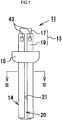
- the ceramic heater 11 includes: a cylindrical ceramic heater body 13 made of ceramic; and an annular flange 15 made of metal, externally fitted to the heater body 13.
- the flange 15 is an annular member formed by bending a metal plate such as a stainless-steel plate.
- the flange 15 has a recessed (cup-shaped) center portion.
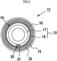
- a space surrounded by an outer peripheral surface 14 of the heater body 13 and an inner surface of the flange 15 serves as a glass reservoir 35.
- the glass reservoir 35 is filled with glass 33, and the heater body 13 and the flange 15 are welded and fixed via the glass 33.
- the glass 33 is shown by hatching.
- the heater body 13 is composed of: a cylindrical support member 17 made of ceramic; and a ceramic sheet 19 wrapped around the outer periphery of the support member 17.
- the support member 17 and the ceramic sheet 19 are formed by using ceramic such as alumina (Al 2 O 3 ).
- the thermal expansion coefficient of alumina is within a range of 50 ⁇ 10 -7 /K to 90 ⁇ 10 -7 /K, and is 70 ⁇ 10 -7 /K (30°C to 380°C) in the present embodiment.
- the support member 17 has an outer diameter set to 12 mm, an inner diameter set to 8 mm, and a length set to 65 mm.
- the ceramic sheet 19 has a thickness set to 0.5 mm, and a length set to 60 mm.
- the ceramic sheet 19 does not completely cover the outer periphery of the support member 17. Therefore, a slit 21 is formed at a wrapping-ends meeting portion 20 of the ceramic sheet 19.
- the slit 21 extends along an axial direction of the support member 17, and exposes an outer peripheral surface of the support member 17.
- the slit 21 of the present embodiment has a width set to 1 mm, and a depth set to 0.5 mm.
- a heater wire 41 having a meandering pattern and a pair of internal terminals 42 are formed inside the ceramic sheet 19, a heater wire 41 having a meandering pattern and a pair of internal terminals 42 are formed.
- the heater wire 41 and the internal terminals 42 contain tungsten (W) as a main component.
- the internal terminals 42 are electrically connected to external terminals 43 (refer to FIG. 1 ) formed on an outer peripheral surface of the ceramic sheet 19, through via conductors (not shown) or the like.
- the heater wire 41 includes: a plurality of wiring portions 44 extending along the axial direction of the support member 17; and connection portions 45 each connecting adjacent wiring portions 44 to each other.
- the plurality of wiring portions 44 include a pair of outer wiring portions 46, and a plurality of inner wiring portions 47.
- the pair of outer wiring portions 46 are disposed on opposite sides from each other with the wrapping-ends meeting portion 20 (refer to FIG. 3 ) of the ceramic sheet 19 therebetween.
- a first end (upper end in FIG. 4 ) of each outer wiring portion 46 is connected to an internal terminal 42, and a second end (lower end in FIG. 4 ) of the outer wiring portion 46 is connected to an inner wiring portion 47 via a connection portion 45.
- the internal terminals 42 are disposed between the pair of outer wiring portions 46 when the ceramic sheet 19 is viewed in the thickness direction.
- each inner wiring portion 47 is disposed between the pair of outer wiring portions 46.
- a first end (upper end in FIG. 4 ) of each inner wiring portion 47 is connected to a first end of an adjacent inner wiring portion 47 via a connection portion 45.
- a second end (lower end in FIG. 4 ) of each inner wiring portion 47 is connected to a second end of an adjacent inner wiring portion 47 or to a second end of an adjacent outer wiring portion 46, via a connection portion 45.
- Each outer wiring portion 46 of the present embodiment has a line width W1 set to 0.66 mm and a thickness set to 15 ⁇ m.
- Each inner wiring portion 47 of the present embodiment has a line width W2 set to 0.60 mm and a thickness set to 15 ⁇ m.
- each connection portion 45 of the present embodiment has a line width W3 set to 0.60 mm and a thickness set to 15 ⁇ m. That is, the line width W1 of the outer wiring portion 46 is larger than the line width W2 of the inner wiring portion 47 and the line width W3 of the connection portion 45.
- the line width W1 of the outer wiring portion 46 is set to be 1.1 times the line width W2 of the inner wiring portion 47 and the line width W3 of the connection portion 45.
- the line width W2 of the inner wiring portion 47 is equal to the line width W3 of the connection portion 45. Since the thickness of the outer wiring portion 46 is equal to the thickness of the inner wiring portion 47 and to the thickness of the connection portion 45, the cross-sectional area of the outer wiring portion 46 is larger than the cross-sectional area of the inner wiring portion 47 and the cross-sectional area of the connection portion 45.
- a clayey slurry containing alumina as a main component is put in a conventionally known extruder (not shown), and the slurry is molded into a tubular member. Then, the molded tubular member is dried, and thereafter is subjected to pre-firing in which the cylindrical member is heated to a predetermined temperature (e. g., about 1000°C), thereby obtaining the support member 17 (refer to FIG. 5A ).
- a predetermined temperature e. g., about 1000°C
- first and second ceramic green sheets 51 and 52 which will become the ceramic sheet 19, are formed.
- a known formation method such as a doctor blade method can be adopted.
- a conductive paste tungsten paste in the present embodiment
- an unfired electrode 53 which will become the heater wire 41 and the internal terminals 42, is formed on the surface of the first ceramic green sheet 51 (refer to FIG. 5B ).
- the line width of the unfired electrode 53 is adjusted to be, for example, a width obtained by adding an amount of shrinkage at firing to the line width of the heater wire 41.
- the second ceramic green sheet 52 is stacked on the printed surface (surface on which the unfired electrode 53 is formed) of the first ceramic green sheet 51, and a pressing force is applied in the sheet stacking direction. As a result, the ceramic green sheets 51 and 52 are unified, thereby forming a green-sheet stacked body 54 (refer to FIG. 5C ). Further, using the paste printing apparatus, a conductive paste is printed on the surface of the second ceramic green sheet 52. As a result, an unfired electrode 55, which will become the external terminals 43, is formed on the surface of the second ceramic green sheet 52.
- a ceramic paste (alumina paste) is applied to one side of the green-sheet stacked body 54, and the green-sheet stacked body 54 is wrapped around the outer peripheral surface of the support member 17 so as to be adhered to the support member 17 (refer to FIG. 5D ).
- the size of the green-sheet stacked body 54 is adjusted so that the opposing ends of the green-sheet stacked body 54 do not overlap each other.
- a drying process, a degreasing process, etc. are performed according to conventionally known techniques, and thereafter, co-firing is performed in which the green-sheet stacked body 54 (the ceramic green sheets 51 and 52, and the unfired electrodes 53 and 55) is heated to a predetermined temperature (e.
- alumina in the ceramic green sheets 51 and 52 and tungsten in the conductive paste are simultaneously sintered, whereby the green-sheet stacked body 54 becomes the ceramic sheet 19, the unfired electrode 53 becomes the heater wire 41 and the internal terminals 42, and the unfired electrode 55 becomes the external terminals 43. Thereafter, the external terminals 43 are plated with nickel to obtain the heater body 13.
- a plate member made of stainless steel is press-formed using a die, thereby forming the cup-shaped flange 15. Then, the flange 15 is externally fitted to the heater body 13 at a predetermined position. Thereafter, the heater body 13 and the flange 15 are welded and fixed via the glass 33 to complete the ceramic heater 11.
- a ceramic heater was prepared which includes a ceramic sheet having a line width of each outer wiring portion being 0.60 mm, a line width of each inner wiring portion being 0.60 mm, and a value of a ratio of the line width of the outer wiring portion to the line width of the inner wiring portion being 1.0.
- a ceramic heater in which the line width of each outer wiring portion was equal to the line width of each inner wiring portion was prepared.
- This ceramic heater was regarded as a sample 1A.
- a ceramic heater having a line width of each outer wiring portion being 0.64 mm, a line width of each inner wiring portion being 0.60 mm, and a value of the ratio being 1.07 was prepared as a sample 1B.
- a ceramic heater having a line width of each outer wiring portion being 0.60 mm, a line width of each inner wiring portion being 0.55 mm, and a value of the ratio being 1.09 was prepared as a sample 1C.
- a ceramic heater having a line width of each outer wiring portion being 0.69 mm, a line width of each inner wiring portion being 0.60 mm, and a value of the ratio being 1.15 was prepared as a sample 1E.
- a ceramic heater having a line width of each outer wiring portion being 1.20 mm, a line width of each inner wiring portion being 0.60 mm, and a value of the ratio being 2.0 was prepared as a sample 1F.
- a ceramic heater having a line width of each outer wiring portion being 1.44 mm, a line width of each inner wiring portion being 0.60 mm, and a value of the ratio being 2.4 was prepared as a sample 1G.
- a nichrome wire was soldered to a pair of internal terminals (heater wire) included in the ceramic sheet of each of the measurement samples (samples 1A to 1G), and each measurement sample, in its dry state, was placed on a base. Then, a voltage (AC 240V) was applied across the pair of internal terminals for 6 minutes, and the surface temperature of the ceramic sheet was measured by a thermocamera. In addition, it was observed whether local heat generation occurred at the outer wiring portions and whether dielectric breakdown occurred between the pair of outer wiring portions. If dielectric breakdown occurred, the occurrence time was measured and recorded. The results are shown on Table 1.
- sample 1A it was found that, in all the five samples, local heat generation occurred, and dielectric breakdown occurred with a spark after 1 min and 50 sec had passed.
- sample 1B it was found that local heat generation occurred in all the five samples, and dielectric breakdown occurred in two samples among the five samples.
- samples 1C to 1G neither local heat generation nor dielectric breakdown was found in any of the five samples throughout observation for 6 minutes.
- sample 1G it was found that the temperature at the wrapping-ends meeting portion of the ceramic sheet was reduced, leading to reduction in thermal uniformity.
- each of outer wiring portions 63 as components of a heater wire 62 has: a line width W4, at a center portion 64, set to 0.66 mm; a line width W5, at a portion 65 other than the center portion 64, set to 0.60 mm; and a thickness set to 15 ⁇ m.
- the "center portion 64 of the outer wiring portion 63" is a region, of a center portion of the outer wiring portion 63, which occupies not larger than one-third of the length of the outer wiring portion 63.
- each of inner wiring portions 66 as components of the heater wire 62 has a line width W6 set to 0.60 mm, and a thickness set to 15 ⁇ m.
- each of connection portions 67 as components of the heater wire 62 also has a line width W7 set to 0.60 mm, and a thickness set to 15 ⁇ m. That is, the line width W4 of the center portion 64 of the outer wiring portion 63 is larger than the line width W5 of the other portion 65 of the outer wiring portion 63, the line width W6 of the inner wiring portion 66, and the line width W7 of the connection portion 67. Specifically, the line width W4 of the center portion 64 is set to be 1.1 times the line width W5 of the other portion 65, the line width W6 of the inner wiring portion 66, and the line width W7 of the connection portion 67.
- the cross-sectional area of the center portion 64 is larger than the cross-sectional area of the other portion 65, the cross-sectional area of the inner wiring portion 66, and the cross-sectional area of the connection portion 67.
- the line width of the outer wiring portion 63 gradually increases from the other portion 65 to the center portion 64.
- a ceramic heater was prepared which includes a ceramic sheet having a line width of the center portion of each outer wiring portion being 0.60 mm, a line width of each inner wiring portion being 0.55 mm, and a value of a ratio of the line width of the center portion to the line width of the inner wiring portion being 1.09.
- This ceramic heater was regarded as a sample 1C'.
- a ceramic heater having a line width of the center portion being 0.66 mm, a line width of each inner wiring portion being 0.60 mm, and a value of the ratio being 1.1 that is, a ceramic heater identical to the ceramic heater of the present embodiment, was prepared as a sample 1D'.
- a ceramic heater having a line width of the center portion being 0.69 mm, a line width of each inner wiring portion being 0.60 mm, and a value of the ratio being 1.15 was prepared as a sample 1E'.
- a ceramic heater having a line width of the center portion being 1.20 mm, a line width of each inner wiring portion being 0.60 mm, and a value of the ratio being 2.0 was prepared as a sample 1F'.
- a ceramic heater 111 according to the present embodiment is used in, for example, a heat exchanger of a heat exchange unit of a warm water washing toilet seat, for the purpose of warming washing water.
- the ceramic heater 111 includes: a cylindrical ceramic heater body 113 made of ceramic; and an annular flange 115 made of metal, externally fitted to the heater body 113.
- the flange 115 is an annular member formed by bending a metal plate such as a stainless-steel plate.
- the flange 115 has a recessed (cup-shaped) center portion.
- a space surrounded by an outer peripheral surface 114 of the heater body 113 and an inner surface of the flange 115 serves as a glass reservoir 135.
- the glass reservoir 135 is filled with glass 133, and the heater body 113 and the flange 115 are welded and fixed via the glass 133.
- the glass 133 is shown by hatching.
- the heater body 113 is composed of: a cylindrical support member 117 made of ceramic; and a ceramic sheet 119 wrapped around the outer periphery of the support member 117.
- the support member 117 and the ceramic sheet 119 are formed by using ceramic such as alumina (Al 2 O 3 ).
- the thermal expansion coefficient of alumina is within a range of 50 ⁇ 10 -7 /K to 90 ⁇ 10 -7 /K, and is 70 ⁇ 10 -7 /K (30°C to 380°C) in the present embodiment.
- the support member 117 has an outer diameter set to 12 mm, an inner diameter set to 8 mm, and a length set to 65 mm.
- the ceramic sheet 119 has a thickness set to 0.5 mm, and a length set to 60 mm.
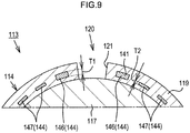
- the ceramic sheet 119 does not completely cover the outer periphery of the support member 117. Therefore, a slit 121 is formed at a wrapping-ends meeting portion 120 of the ceramic sheet 119.
- the slit 121 extends along an axial direction of the support member 117, and exposes an outer peripheral surface of the support member 117.
- the slit 121 of the present embodiment has a width set to 1 mm, and a depth set to 0.5 mm.
- a heater wire 141 having a meandering pattern and a pair of internal terminals 142 are formed inside the ceramic sheet 119.
- the heater wire 141 and the internal terminals 142 contain tungsten (W) as a main component.
- the internal terminals 142 are electrically connected to external terminals 143 (refer to FIG. 7 ) formed on an outer peripheral surface of the ceramic sheet 119, through via conductors (not shown) or the like.
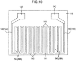
- the heater wire 141 includes: a plurality of wiring portions 144 extending along the axial direction of the support member 117; and connection portions 145 each connecting adjacent wiring portions 144 to each other.
- the wiring portions 144 include a pair of outer wiring portions 146, and a plurality of inner wiring portions 147.
- the outer wiring portions 146 are disposed on opposite sides from each other with a wrapping-ends meeting portion 120 (refer to FIG. 9 ) of the ceramic sheet 119 therebetween.
- a first end (upper end in FIG. 10 ) of each outer wiring portion 146 is connected to an internal terminal 142, and a second end (lower end in FIG. 10 ) of each outer wiring portion 146 is connected to an inner wiring portion 147 via a connection portion 145.
- the internal terminals 142 are disposed between the pair of outer wiring portions 146 when the ceramic sheet 119 is viewed in the thickness direction.
- each inner wiring portion 147 is disposed between the pair of outer wiring portions 146.
- a first end (upper end in FIG. 10 ) of each inner wiring portion 147 is connected to a first end of an adjacent inner wiring portion 147 via a connection portion 145.
- a second end (lower end in FIG. 10 ) of each inner wiring portion 147 is connected to a second end of an adjacent inner wiring portion 147 or to a second end of an adjacent outer wiring portion 146, via a connection portion 145.
- Each outer wiring portion 146 of the present embodiment has a thickness T1 set to 20 ⁇ m, and a line width set to 0.60 mm.
- Each inner wiring portion 147 of the present embodiment has a thickness T2 set to 15 ⁇ m, and a line width set to 0.60 mm.
- each connection portion 145 of the present embodiment has a thickness set to 15 ⁇ m, and a line width set to 0.60 mm. That is, the thickness T1 of the outer wiring portion 146 is larger than the thickness T2 of the inner wiring portion 147 and the thickness of the connection portion 145.
- the thickness T1 of the outer wiring portion 146 is set to be 1.33 times the thickness T2 of the inner wiring portion 147 and the thickness of the connection portion 145.
- the thickness T2 of the inner wiring portion 147 is equal to the thickness of the connection portion 145. Since the line width of the outer wiring portion 146 is equal to the line width of the inner wiring portion 147 and to the line width of the connection portion 145, the cross-sectional area of the outer wiring portion 146 is larger than the cross-sectional area of the inner wiring portion 147 and the cross-sectional area of the connection portion 145.
- a clayey slurry containing alumina as a main component is put in a conventionally known extruder (not shown), and the slurry is molded into a tubular member. Then, the molded tubular member is dried, and thereafter is subjected to pre-firing in which the cylindrical member is heated to a predetermined temperature (e. g., about 1000°C), thereby obtaining the support member 117 (refer to FIG. 11A ).
- a predetermined temperature e. g., about 1000°C
- first and second ceramic green sheets 151 and 152 which will become the ceramic sheet 119, are formed.
- a known formation method such as a doctor blade method can be adopted.
- a printing process is performed by using a conventionally known paste printing apparatus (not shown), to print a conductive paste (tungsten paste in the present embodiment) on the surface of the first ceramic green sheet 151.
- the conductive paste is printed dividedly in two times to make the thickness T1 of the outer wiring portion 146 larger than the thickness T2 of the inner wiring portion 147.
- the conductive paste is printed on the surface of the first ceramic green sheet 151, thereby forming a first electrode 153 as an unfired electrode which forms the heater wire 141 and the internal terminals 142 (refer to FIG. 11B ).
- the line width of the first electrode 153 is adjusted to be, for example, a width obtained by adding an amount of shrinkage at firing to the line width of the heater wire 141.
- the conductive paste is printed on portions, of the first electrode 153, which will become the outer wiring portions 146, thereby forming a second electrode 154 which forms portions of the outer wiring portions 146 (refer to FIG. 11B ).
- the line width of the second electrode 154 is adjusted to be narrower than that of the first electrode 153, for example.
- a second ceramic green sheet 152 is stacked on the printed surface (surface on which the first electrode 153 and the second electrode 154 are formed) of the first ceramic green sheet 151, and a pressing force is applied in the sheet stacking direction.
- the ceramic green sheets 151 and 152 are unified, thereby forming a green-sheet stacked body 155 (refer to FIG. 11C ).
- the conductive paste is printed on the surface of the second ceramic green sheet 152.
- an unfired electrode 156 which will become the external terminals 143, is formed on the surface of the second ceramic green sheet 152.
- a wrapping process is performed in which a ceramic paste (alumina paste) is applied to one side of the green-sheet stacked body 155, and the green-sheet stacked body 155 is wrapped around the outer peripheral surface of the support member 117 so as to be adhered to the support member 117 (refer to FIG. 11D ).
- the size of the green-sheet stacked body 155 is adjusted so that the opposing ends of the green-sheet stacked body 155 do not overlap each other.
- the green-sheet stacked body 155 (the ceramic green sheets 151 and 152, the first electrode 153, the second electrode 154, and the unfired electrode 156) is heated to a predetermined temperature (e.g., about 1400°C to 1600°C) at which alumina and tungsten in the green-sheet stacked body 155 can be sintered.
- a predetermined temperature e.g., about 1400°C to 1600°C
- the green-sheet stacked body 155 becomes the ceramic sheet 119
- the electrodes 153 and 154 become the heater wire 141 and the internal terminal 142, respectively
- the unfired electrode 156 becomes the external terminals 143.
- the external terminals 143 are plated with nickel to obtain the heater body 113.
- a plate member made of stainless steel is press-formed using a die, thereby forming the cup-shaped flange 115.
- the flange 115 is externally fitted to the heater body 113 at a predetermined position. Thereafter, the heater body 113 and the flange 115 are welded and fixed via the glass 133 to complete the ceramic heater 111.
- a ceramic heater was prepared which includes a ceramic sheet having a thickness of each outer wiring portion being 15 ⁇ m, a thickness of each inner wiring portion being 15 ⁇ m, and a value of a ratio of the thickness of the outer wiring portion to the thickness of the inner wiring portion being 1.0.
- a ceramic heater in which the thickness of each outer wiring portion is equal to the thickness of each inner wiring portion was prepared.
- This ceramic heater was regarded as a sample 2A.
- a ceramic heater having a thickness of each outer wiring portion being 18 ⁇ m, a thickness of each inner wiring portion being 15 ⁇ m, and a value of the ratio being 1.2 was prepared as a sample 2B.
- a ceramic heater having a thickness of each outer wiring portion being 15 ⁇ m, a thickness of each inner wiring portion being 12 ⁇ m, and a value of the ratio being 1.25 was prepared as a sample 2C.
- a ceramic heater having a thickness of each outer wiring portion being 19 ⁇ m, a thickness of each inner wiring portion being 15 ⁇ m, and a value of the ratio being 1.27 was prepared as a sample 2D.
- a ceramic heater having a thickness of the outer wiring portion being 25 ⁇ m, a thickness of the inner wiring portion being 15 ⁇ m, and a value of the ratio being 1.67 was prepared as a sample 2F.
- a ceramic heater having a thickness of each outer wiring portion being 30 ⁇ m, a thickness of each inner wiring portion being 15 ⁇ m, and a value of the ratio being 2.0 was prepared as a sample 2G.
- a ceramic heater having a thickness of each outer wiring portion being 36 ⁇ m, a thickness of each inner wiring portion being 15 ⁇ m, and a value of the ratio being 2.4 was prepared as a sample 2H. As for each of the samples 2A to 2H, five samples were prepared.
- a nichrome wire was soldered to a pair of internal terminals (heater wire) included in the ceramic sheet of each of the measurement samples (samples 2A to 2H), and each measurement sample, in its dry state, was placed on a base. Then, a voltage (AC 240V) was applied across the pair of internal terminals for 6 minutes, and the surface temperature of the ceramic sheet was measured by a thermocamera. In addition, it was observed whether local heat generation occurred at the outer wiring portions and whether dielectric breakdown occurred between the pair of outer wiring portions. If dielectric breakdown occurred, the occurrence time was measured and recorded. The results are shown on Table 3.
- the sample 2A it was found that, in all the five samples, local heat generation occurred, and dielectric breakdown occurred with a spark after 1 min and 50 sec had passed.
- the sample 2B it was found that local heat generation occurred in all the five samples, and dielectric breakdown occurred in two samples among the five samples.
- the sample 2C occurrence of dielectric breakdown was not found, but local heat generation was found in one sample among the five samples.
- the samples 2D to 2H neither local heat generation nor dielectric breakdown was found in any of the five samples throughout observation for 6 minutes. However, in the sample 2H, it was found that the temperature at the wrapping-ends meeting portion of the ceramic sheet was reduced, leading to reduction in thermal uniformity.
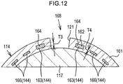
- each of outer wiring portions 163 as components of a heater wire 162 included in a ceramic sheet 161 has: a thickness T3, of a center portion 164, set to 20 ⁇ m; a thickness, of a portion 165 other than the center portion 164, set to 15 ⁇ m; and a line width set to 0.60 mm.
- the "center portion 164 of the outer wiring portion 163" is a region, of a center portion of the outer wiring portion 163, which occupies not larger than one-third of the length of the outer wiring portion 163.
- Each of inner wiring portions 166 as components of the heater wire 162 has a thickness T4 set to 15 ⁇ m, and a line width set to 0.60 mm.
- each of connection portions 167 as components of the heater wire 162 also has a thickness set to 15 ⁇ m, and a line width set to 0.60 mm. That is, the thickness T3 of the center portion 164 of the outer wiring portion 163 is larger than the thickness of the other portion 165 of the outer wiring portion 163, the thickness T4 of the inner wiring portion 166, and the thickness of the connection portion 167. Specifically, the thickness T3 of the center portion 164 is set to be 1.33 times the thickness of the other portion 165, the thickness T4 of the inner wiring portion 166, and the thickness of the connection portion 167.
- the cross-sectional area of the center portion 164 is larger than the cross-sectional area of the other portion 165, the cross-sectional area of the inner wiring portion 166, and the cross-sectional area of the connection portion 167.
- the conductive paste is printed dividedly in two times, to make the thickness T3 of the center portion 164 larger than the thickness T4 of the inner wiring portion 166. Specifically, first, the conductive paste is printed on the surface of a ceramic green sheet which will become the ceramic sheet 161, thereby forming a first electrode as an unfired electrode which forms the heater wire 162. Next, the conductive paste is printed on portions, of the first electrode, which will become the center portions 164, thereby forming a second electrode which form portions of the center portions 164.
- the line width of the second electrode is adjusted so as to be narrower than that of the first electrode, for example.
- a ceramic heater was prepared which includes a ceramic sheet having a thickness of the center portion of each outer wiring portion being 15 ⁇ m, a thickness of each inner wiring portion being 12 ⁇ m, and a value of a ratio of the thickness of the center portion to the thickness of the inner wiring portion being 1.25.
- This ceramic heater was regarded as a sample 2C'.
- a ceramic heater having a thickness of the center portion being 20 ⁇ m, a thickness of each inner wiring portion being 15 ⁇ m, and a value of the ratio being 1.33 was prepared as a sample 2E'.
- a ceramic heater having a thickness of the center portion being 25 ⁇ m, a thickness of each inner wiring portion being 15 ⁇ m, and a value of the ratio being 1.67 was prepared as a sample 2F'.
- a ceramic heater having a thickness of the center portion being 30 ⁇ m, a thickness of each inner wiring portion being 15 ⁇ m, and a value of the ratio being 2.0 was prepared as a sample 2G'.
- each outer wiring portion 163 when the thickness T3 of the center portion 164 of each outer wiring portion 163 is larger than the thickness T4 of each inner wiring portion 166, electric resistance of the center portion 164 becomes smaller than that of the inner wiring portion 166. Therefore, at the wrapping-ends meeting portion 168 of the ceramic sheet 161, where the outer wiring portions 163 are positioned, local heat generation of the heater wire 162 can be suppressed. As a result, melting of the glass component present in the ceramic sheet 161 near the center portions 164 of the outer wiring portions 163 is suppressed, thereby inhibiting dielectric breakdown between the pair of outer wiring portions 163, and inhibiting breakage of the ceramic heater. Therefore, reliability of the ceramic heater can be improved. [Other embodiments] The above-described embodiments may be modified as follows.
- the line width W3 of the connection portion 45 may be larger than the line width W1 of the outer wiring portion 46 and the line width W2 of the inner wiring portion 47.
- the line width W7 of the connection portion 67 may be larger than the line width W4 of the center portion 64 of the outer wiring portion 63, the line width W5 of the other portion 65 of the outer wiring portion 63, and the line width W6 of the inner wiring portion 66.
- one center portion 64 is formed in one outer wiring portion 63.
- two or more wide portions each having the same line width as the center portion 64 may be formed in one outer wiring portion.
- the respective wide portions may be disposed apart from each other along the direction in which the outer wiring portion extends, or may be disposed in contact with each other along the direction in which the outer wiring portion extends.
- the support member 17 of the ceramic heater 11 and the support member 117 of the ceramic heater 111 are tubular in shape.
- these support members each may have a rod shape. That is, the ceramic heaters may be used in equipment (e. g., a fan heater) other than a warm water washing toilet seat.
- the flange made of stainless steel is used.
- a flange made of alumina may be used, for example.
- the ceramic heater 11 and the ceramic heater 111 are configured such that an AC voltage is applied across the pair of internal terminals 42 and across the pair of internal terminals 142, respectively.
- a DC voltage may be applied across the pair of internal terminals 42 and across the pair of internal terminals 142.
- the conductive paste is printed dividedly in two times to make the thickness T1 of the outer wiring portion 146 larger than the thickness T2 of the inner wiring portion 147.
- the conductive paste may be printed dividedly in three or more times to make the thickness T1 of the outer wiring portion 146 larger than the thickness T2 of the inner wiring portion 147.
- the conductive paste is printed dividedly in two times to make the thickness T3 of the center portion 164 larger than the thickness T4 of the inner wiring portion 166.
- the conductive paste may be printed dividedly in three or more times to make the thickness T3 of the center portion 164 larger than the thickness T4 of the inner wiring portion 166.
- the conductive paste is printed on the surface of the first ceramic green sheet 151 to form the unfired electrode (first electrode 153) which forms almost the entirety of the heater wire 141 (region excluding upper-layer portions of the outer wiring portions 146). Thereafter, the conductive paste is printed on portions, of the first electrode 153, which will become the outer wiring portions 146, to form the unfired electrode (second electrode 154) which forms the upper-layer portions of the outer wiring portions 146.
- the conductive paste may be printed on portions, of the surface of the first ceramic green sheet 151, which will become the outer wiring portions 146, to form the unfired electrode which forms lower-layer portions of the outer wiring portions 146.
- the conductive paste may be printed on the unfired electrode and the surface of the first ceramic green sheet 151 to form the unfired electrode which forms almost the entirety of the heater wire 141 (region excluding the lower-layer portions of the outer wiring portions 146).
- the entirety of the heater wire 141 may be formed by performing printing of the conductive paste only one time by using an ink-jet apparatus or the like.
- the conductive paste is printed on the surface of the ceramic green sheet to form the unfired electrode (first electrode) which forms almost the entirety of the heater wire 162 (region excluding upper-layer portions of the center portions 164). Thereafter, the conductive paste is printed on portions, of the first electrode, which will become the center portions 164, to form the unfired electrode (second electrode) which forms the upper-layer portions of the center portions 164.
- the conductive paste may be printed on portions, of the surface of the ceramic green sheet, which will become the center portions 164 to form the unfired electrode which forms lower-layer portions of the center portions 164.
- the conductive paste may be printed on the unfired electrode and the surface of the ceramic green sheet to form the unfired electrode which forms almost the entirety of the heater wire 162 (region excluding the lower-layer portions of the center portions 164).
- the entirety of the heater wire 162 may be formed by performing printing of the conductive paste only one time by using an ink-jet apparatus or the like.
- the line width of the second electrode 154 which will become the outer wiring portions 146 is adjusted to be narrower than that of the first electrode 153 which also will become the outer wiring portions 146.
- the line width of the second electrode 154 may be equal to that of the first electrode 153, or may be larger than that of the first electrode 153.
- the line width of the second electrode which will become the center portions 164 is adjusted to be narrower than the first electrode which also will become the center portions 164.
- the line width of the second electrode may be equal to that of the first electrode, or may be larger than that of the first electrode.
- the ceramic heaters 11 and 111 each correspond to an example of a ceramic heater
- the support members 17 and 117 each correspond to an example of a support member
- the ceramic sheets 19, 61, 119, and 161 each correspond to an example of a ceramic sheet.
- the wrapping-ends meeting portions 20, 120, and 168 each correspond to an example of a wrapping-ends meeting portion
- the heater wires 41, 62, 141, and 162 each correspond to an example of a heater wire
- the wiring portions 44 and 144 each correspond to an example of a wiring portion
- the connection portions 45, 67, 145, and 167 each correspond to an example of a connection portion.
- the outer wiring portions 46, 63, 146, and 163 each correspond to an example of an outer wiring portion
- the inner wiring portions 47, 66, 147, and 166 each correspond to an example of an inner wiring portion
- the center portions 64 and 164 of the outer wiring portions each correspond to an example of a center portion of an outer wiring portion.
Landscapes
- Chemical & Material Sciences (AREA)
- Engineering & Computer Science (AREA)
- Ceramic Engineering (AREA)
- Inorganic Chemistry (AREA)
- Resistance Heating (AREA)
- Surface Heating Bodies (AREA)
Abstract
Description
- This international patent application claims priority based on Japanese Patent Application No.
2016-051823 2016-051824 2016-051823 2016-051824 - The present disclosure relates to a ceramic heater for use in a warm water washing toilet seat, a fan heater, an electric water heater, a 24-hour bath, a soldering iron, a hair iron, etc. In particular, the present disclosure relates to a ceramic heater having a structure in which a ceramic sheet having a heater wire is wrapped around an outer periphery of a support member.
- Generally, a heat exchange unit having a resin container (heat exchanger) is used in a warm water washing toilet seat. A tubular ceramic heater is mounted to the heat exchange unit to warm washing water stored in the heat exchanger.
- As for this type of ceramic heater, a ceramic heater has been known which is formed by wrapping a ceramic sheet, on which a heater wire is printed, around a cylindrical ceramic support member, and integrally firing the ceramic sheet and the support member (e. g., refer to Patent Document 1).
- Patent Document 1: Japanese Patent No.
3038039 - A ceramic heater for a warm water washing toilet seat is used in water at all times, and therefore is hardly energized and heated while it is in a dry state. Meanwhile, when water supply is cut off or piping is in trouble, there is a possibility that the ceramic heater is energized and heated in its dry state. However, since the cross-sectional area (e. g., line width, thickness) of a general heater wire is uniform, if the ceramic heater is heated in its dry state, the heater wire locally generates heat at a wrapping-ends meeting portion of the ceramic sheet, which may cause melting of a glass component present in the ceramic sheet near the heat-generating heater wire. In this case, since electrons become easy to move, partial discharge occurs between a pair of heater wire portions positioned on opposite sides from each other with the wrapping-ends meeting portion therebetween, which may result in dielectric breakdown. Moreover, a ceramic component present in the ceramic sheet is also melted due to a spark that occurs during the partial discharge, which may result in breakage of the ceramic heater.
- According to one aspect of the present disclosure, it is desirable to provide a ceramic heater capable of improving reliability thereof by inhibiting dielectric breakdown that may occur in a heater wire.
- One aspect of the present disclosure is a ceramic heater including a support member made of ceramic, and a ceramic sheet which is wrapped around an outer periphery of the support member, and includes a heater wire. The heater wire includes a plurality of wiring portions and a connection portion. The plurality of wiring portions include a pair of outer wiring portions, and an inner wiring portion. Each outer wiring portion has a cross-sectional area larger than that of the inner wiring portion.
- The plurality of wiring portions are configured to extend along the axial direction of the support member. The connection portion is configured to connect adjacent wiring portions. The pair of outer wiring portions are disposed on opposite sides from each other with a wrapping-ends meeting portion of the ceramic sheet therebetween. The inner wiring portion is disposed, in the ceramic sheet, between the pair of outer wiring portions.
- In this ceramic heater, the cross-sectional area of each of the pair of outer wiring portions positioned on opposite sides from each other with the wrapping-ends meeting portion of the ceramic sheet therebetween, is set to be larger than the cross-sectional area of the inner wiring portion disposed, in the ceramic sheet, between the pair of outer wiring portions, whereby electric resistance of the outer wiring portion becomes smaller than that of the inner wiring portion. Thus, local heat generation of the heater wire can be suppressed at the wrapping-ends meeting portion where the outer wiring portions are positioned. As a result, melting of a glass component present in the ceramic sheet near the outer wiring portions is suppressed, thereby inhibiting dielectric breakdown between the pair of outer wiring portions, and inhibiting breakage of the ceramic heater. Therefore, reliability of the ceramic heater can be improved.
- As an example of the structure in which the cross-sectional area of the outer wiring portion is larger than that of the inner wiring portion, a structure in which the line width of the outer wiring portion is larger than that of the inner wiring portion is considered. That is, when the line width of each of the pair of outer wiring portions is set to be larger than that of the inner wiring portion, electric resistance of the outer wiring portion becomes smaller than that of the inner wiring portion, whereby local heat generation of the heater wire can be suppressed.
- The line width of the outer wiring portion may be set to be larger than 1.07 times and smaller than 2.4 times the line width of the inner wiring portion. When the line width of the outer wiring portion is set to be larger than 1.07 times the line width of the inner wiring portion, it is possible to suppress local heat generation of the outer wiring portion, and inhibit occurrence of dielectric breakdown between the pair of outer wiring portions positioned on opposite sides from each other with the wrapping-ends meeting portion therebetween. Meanwhile, when the line width of the outer wiring portion is set to be smaller than 2.4 times the line width of the inner wiring portion, it is possible to suppress local temperature reduction in the outer wiring portion, thereby inhibiting reduction in thermal uniformity.
- As an example of the structure in which the cross-sectional area of the outer wiring portion is larger than that of the inner wiring portion, a structure in which the thickness of the outer wiring portion is larger than that of the inner wiring portion is considered. That is, when the thickness of each of the pair of outer wiring portions is set to be larger than that of the inner wiring portion, electric resistance of the outer wiring portion becomes smaller than that of the inner wiring portion.
- The thickness of the outer wiring portion may be set to be larger than 1.25 times and smaller than 2.4 times the thickness of the inner wiring portion. When the thickness of the outer wiring portion is set to be larger than 1.25 times the thickness of the inner wiring portion, it is possible to suppress local heat generation of the outer wiring portion, and inhibit occurrence of dielectric breakdown between the pair of outer wiring portions positioned on opposite sides from each other with the wrapping-ends meeting portion therebetween. Meanwhile, when the thickness of the outer wiring portion is set to be smaller than 2.4 times the thickness of the inner wiring portion, it is possible to suppress local temperature reduction in the outer wiring portion, thereby inhibiting reduction in thermal uniformity.
- Another aspect of the present disclosure is a ceramic heater including a support member made of ceramic, and a ceramic sheet which is wrapped around an outer periphery of the support member, and includes a heater wire. The heater wire includes a plurality of wiring portions and a connection portion. The plurality of wiring portions include a pair of outer wiring portions, and an inner wiring portion. A center portion of each outer wiring portion has a cross-sectional area larger than that of the inner wiring portion.
- The plurality of wiring portions are configured to extend along the axial direction of the support member. The connection portion is configured to connect adjacent wiring portions. The pair of outer wiring portions are disposed on opposite sides from each other with a wrapping-ends meeting portion of the ceramic sheet therebetween. The inner wiring portion is disposed, in the ceramic sheet, between the pair of outer wiring portions.
- In this ceramic heater, the cross-sectional area of the center portion of each of the pair of outer wiring portions positioned on opposite sides from each other with the wrapping-ends meeting portion of the ceramic sheet therebetween, is set to be larger than the cross-sectional area of the inner wiring portion disposed, in the ceramic sheet, between the pair of outer wiring portions, whereby electric resistance of the center portion of the outer wiring portion becomes smaller than that of the inner wiring portion. Thus, local heat generation of the heater wire can be suppressed at the wrapping-ends meeting portion where the outer wiring portions are positioned. As a result, melting of a glass component present in the ceramic sheet near the center portions of the outer wiring portions is suppressed, thereby inhibiting dielectric breakdown between the pair of outer wiring portions, and inhibiting breakage of the ceramic heater. Therefore, reliability of the ceramic heater can be improved.
- As an example of the structure in which the cross-sectional area of the center portion of the outer wiring portion is larger than that of the inner wiring portion, a structure in which the line width of the center portion of the outer wiring portion is larger than that of the inner wiring portion is considered. That is, when the line width of the center portion of each of the pair of outer wiring portions is set to be larger than that of the inner wiring portion, electric resistance of the center portion of the outer wiring portion becomes smaller than that of the inner wiring portion, whereby local heat generation of the heater wire can be suppressed.
- The line width of the center portion may be set to be larger than 1.07 times and not larger than 2.0 times the line width of the inner wiring portion. When the line width of the center portion is set to be larger than 1.07 times the line width of the inner wiring portion, it is possible to suppress local heat generation of the outer wiring portion, and inhibit occurrence of dielectric breakdown between the pair of outer wiring portions positioned on opposite sides from each other with the wrapping-ends meeting portion therebetween. Meanwhile, when the line width of the center portion is set to be not larger than 2.0 times the line width of the inner wiring portion, it is possible to suppress local temperature reduction in the outer wiring portion, thereby inhibiting reduction in thermal uniformity.
- The above-described ceramic heater includes the support member made of ceramic, and the ceramic sheet wrapped around the outer periphery of the support member. Preferred examples of ceramic that forms the support member and the ceramic sheet may include alumina, aluminum nitride, silicon nitride, boron nitride, zirconia, titania, and mullite. In particular, the support member and the ceramic sheet may contain alumina. In this case, a ceramic heater having excellent heat resistance, chemical resistance, and strength can be produced at reduced costs. The ceramic sheet includes a heater element (heater wire) formed of tungsten, molybdenum, tantalum, or the like. The heater wire may contain, as a main component, at least one of tungsten and molybdenum. In this case, the heater wire can be reliably adhered to the ceramic sheet, whereby reliability of the ceramic heater is further improved.
-
- [
FIG. 1 ] Front view of a ceramic heater according to a first embodiment. - [
FIG. 2 ] Plan view showing the ceramic heater according to the first embodiment. - [
FIG. 3 ] Cross-sectional view taken along a line III-III inFIG. 1 . - [
FIG. 4 ] Explanatory diagram showing a developed ceramic sheet according to the first embodiment. - [
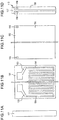
FIG. 5] FIGS. 5A, 5B, 5C, and FIG. 5D being explanatory diagrams showing a ceramic heater production method according to the first embodiment. - [
FIG. 6 ] Explanatory diagram showing a developed ceramic sheet according to a second embodiment. - [
FIG. 7 ] Front view of a ceramic heater according to a third embodiment. - [
FIG. 8 ] Plan view showing the ceramic heater according to the third embodiment. - [
FIG. 9 ] Cross-sectional view taken along a line IX-IX inFIG. 7 . - [
FIG. 10 ] Explanatory diagram showing a developed ceramic sheet according to the third embodiment. - [
FIG. 11] FIGS. 11A, 11B, 11C, and 11D being explanatory diagrams showing a ceramic heater production method according to the third embodiment. - [
FIG. 12 ] Cross-sectional view of a major part including portions of a support member and a ceramic sheet according to a fourth embodiment. - [
FIG. 13 ] Explanatory diagram showing a developed ceramic sheet according to the fourth embodiment. - 11...ceramic heater, 17...support member, 19,61...ceramic sheet, 20...wrapping-ends meeting portion, 41,62...heater wire, 44...wiring portion, 45,67...connection portion, 46,63...outer wiring portion, 47,66...inner wiring portion, 64...center portion of outer wiring portion, W1...line width of outer wiring portion, W2,W6...line width of inner wiring portion, W4...line width of center portion, 111...ceramic heater, 117...support member, 119,161...ceramic sheet, 120,168...wrapping-ends meeting portion, 141,162...heater wire, 144...wiring portion, 145,167...connection portion, 146,163...outer wiring portion, 147,166...inner wiring portion, 164...center portion of outer wiring portion, T1...thickness of outer wiring portion, T2,T4...thickness of inner wiring portion, T3...thickness of center portion
- [First embodiment] Hereinafter, a ceramic heater and a production method therefor according to a first embodiment of the present disclosure will be described with reference to the drawings.
- A
ceramic heater 11 according to the present embodiment is used in, for example, a heat exchanger of a heat exchange unit of a warm water washing toilet seat, for the purpose of warming washing water. - As shown in
FIGS. 1 and2 , theceramic heater 11 includes: a cylindricalceramic heater body 13 made of ceramic; and anannular flange 15 made of metal, externally fitted to theheater body 13. Theflange 15 is an annular member formed by bending a metal plate such as a stainless-steel plate. Theflange 15 has a recessed (cup-shaped) center portion. - In the present embodiment, as shown in
FIG. 2 , in the recessed portion of theflange 15, a space surrounded by an outerperipheral surface 14 of theheater body 13 and an inner surface of theflange 15 serves as aglass reservoir 35. Theglass reservoir 35 is filled withglass 33, and theheater body 13 and theflange 15 are welded and fixed via theglass 33. InFIG. 2 , theglass 33 is shown by hatching. - As shown in
FIGS. 1 to 3 , theheater body 13 is composed of: acylindrical support member 17 made of ceramic; and aceramic sheet 19 wrapped around the outer periphery of thesupport member 17. In the present embodiment, thesupport member 17 and theceramic sheet 19 are formed by using ceramic such as alumina (Al2O3). The thermal expansion coefficient of alumina is within a range of 50×10-7/K to 90×10-7/K, and is 70×10-7/K (30°C to 380°C) in the present embodiment. In the present embodiment, thesupport member 17 has an outer diameter set to 12 mm, an inner diameter set to 8 mm, and a length set to 65 mm. Theceramic sheet 19 has a thickness set to 0.5 mm, and a length set to 60 mm. Theceramic sheet 19 does not completely cover the outer periphery of thesupport member 17. Therefore, aslit 21 is formed at a wrapping-ends meeting portion 20 of theceramic sheet 19. Theslit 21 extends along an axial direction of thesupport member 17, and exposes an outer peripheral surface of thesupport member 17. Theslit 21 of the present embodiment has a width set to 1 mm, and a depth set to 0.5 mm. - As shown in
FIGS. 3 and4 , inside theceramic sheet 19, aheater wire 41 having a meandering pattern and a pair ofinternal terminals 42 are formed. In the present embodiment, theheater wire 41 and theinternal terminals 42 contain tungsten (W) as a main component. Theinternal terminals 42 are electrically connected to external terminals 43 (refer toFIG. 1 ) formed on an outer peripheral surface of theceramic sheet 19, through via conductors (not shown) or the like. - The
heater wire 41 includes: a plurality ofwiring portions 44 extending along the axial direction of thesupport member 17; andconnection portions 45 each connectingadjacent wiring portions 44 to each other. The plurality ofwiring portions 44 include a pair ofouter wiring portions 46, and a plurality ofinner wiring portions 47. The pair ofouter wiring portions 46 are disposed on opposite sides from each other with the wrapping-ends meeting portion 20 (refer toFIG. 3 ) of theceramic sheet 19 therebetween. A first end (upper end inFIG. 4 ) of eachouter wiring portion 46 is connected to aninternal terminal 42, and a second end (lower end inFIG. 4 ) of theouter wiring portion 46 is connected to aninner wiring portion 47 via aconnection portion 45. Theinternal terminals 42 are disposed between the pair ofouter wiring portions 46 when theceramic sheet 19 is viewed in the thickness direction. - As shown in
FIGS. 3 and4 , in theceramic sheet 19, theinner wiring portions 47 are disposed between the pair ofouter wiring portions 46. A first end (upper end inFIG. 4 ) of eachinner wiring portion 47 is connected to a first end of an adjacentinner wiring portion 47 via aconnection portion 45. A second end (lower end inFIG. 4 ) of eachinner wiring portion 47 is connected to a second end of an adjacentinner wiring portion 47 or to a second end of an adjacentouter wiring portion 46, via aconnection portion 45. - Each
outer wiring portion 46 of the present embodiment has a line width W1 set to 0.66 mm and a thickness set to 15 µm. Eachinner wiring portion 47 of the present embodiment has a line width W2 set to 0.60 mm and a thickness set to 15 µm. Likewise, eachconnection portion 45 of the present embodiment has a line width W3 set to 0.60 mm and a thickness set to 15 µm. That is, the line width W1 of theouter wiring portion 46 is larger than the line width W2 of theinner wiring portion 47 and the line width W3 of theconnection portion 45. Specifically, the line width W1 of theouter wiring portion 46 is set to be 1.1 times the line width W2 of theinner wiring portion 47 and the line width W3 of theconnection portion 45. The line width W2 of theinner wiring portion 47 is equal to the line width W3 of theconnection portion 45. Since the thickness of theouter wiring portion 46 is equal to the thickness of theinner wiring portion 47 and to the thickness of theconnection portion 45, the cross-sectional area of theouter wiring portion 46 is larger than the cross-sectional area of theinner wiring portion 47 and the cross-sectional area of theconnection portion 45. - Next, a method of producing the
ceramic heater 11 of the present embodiment will be described. - First, a clayey slurry containing alumina as a main component is put in a conventionally known extruder (not shown), and the slurry is molded into a tubular member. Then, the molded tubular member is dried, and thereafter is subjected to pre-firing in which the cylindrical member is heated to a predetermined temperature (e. g., about 1000°C), thereby obtaining the support member 17 (refer to
FIG. 5A ). - Using a ceramic material containing alumina powder as a main component, first and second ceramic
green sheets ceramic sheet 19, are formed. As for a method of forming the ceramic green sheets, a known formation method such as a doctor blade method can be adopted. Then, using a conventionally known paste printing apparatus (not shown), a conductive paste (tungsten paste in the present embodiment) is printed on the surface of the first ceramicgreen sheet 51. As a result, anunfired electrode 53, which will become theheater wire 41 and theinternal terminals 42, is formed on the surface of the first ceramic green sheet 51 (refer toFIG. 5B ). The line width of theunfired electrode 53 is adjusted to be, for example, a width obtained by adding an amount of shrinkage at firing to the line width of theheater wire 41. - After drying of the conductive paste, the second ceramic
green sheet 52 is stacked on the printed surface (surface on which theunfired electrode 53 is formed) of the first ceramicgreen sheet 51, and a pressing force is applied in the sheet stacking direction. As a result, the ceramicgreen sheets FIG. 5C ). Further, using the paste printing apparatus, a conductive paste is printed on the surface of the second ceramicgreen sheet 52. As a result, anunfired electrode 55, which will become theexternal terminals 43, is formed on the surface of the second ceramicgreen sheet 52. - Next, a ceramic paste (alumina paste) is applied to one side of the green-sheet stacked
body 54, and the green-sheet stackedbody 54 is wrapped around the outer peripheral surface of thesupport member 17 so as to be adhered to the support member 17 (refer toFIG. 5D ). At this time, the size of the green-sheet stackedbody 54 is adjusted so that the opposing ends of the green-sheet stackedbody 54 do not overlap each other. Next, a drying process, a degreasing process, etc. are performed according to conventionally known techniques, and thereafter, co-firing is performed in which the green-sheet stacked body 54 (the ceramicgreen sheets unfired electrodes 53 and 55) is heated to a predetermined temperature (e. g., about 1400°C to 1600°C) at which alumina and tungsten in the green-sheet stackedbody 54 can be sintered. As a result, alumina in the ceramicgreen sheets body 54 becomes theceramic sheet 19, theunfired electrode 53 becomes theheater wire 41 and theinternal terminals 42, and theunfired electrode 55 becomes theexternal terminals 43. Thereafter, theexternal terminals 43 are plated with nickel to obtain theheater body 13. - Next, a plate member made of stainless steel is press-formed using a die, thereby forming the cup-shaped
flange 15. Then, theflange 15 is externally fitted to theheater body 13 at a predetermined position. Thereafter, theheater body 13 and theflange 15 are welded and fixed via theglass 33 to complete theceramic heater 11. - Hereinafter, an example of an experiment performed to evaluate the performance of the
ceramic heater 11 of the present embodiment will be described. - First, measurement samples were prepared as follows. A ceramic heater was prepared which includes a ceramic sheet having a line width of each outer wiring portion being 0.60 mm, a line width of each inner wiring portion being 0.60 mm, and a value of a ratio of the line width of the outer wiring portion to the line width of the inner wiring portion being 1.0. In other words, a ceramic heater in which the line width of each outer wiring portion was equal to the line width of each inner wiring portion was prepared. This ceramic heater was regarded as a sample 1A. Further, a ceramic heater having a line width of each outer wiring portion being 0.64 mm, a line width of each inner wiring portion being 0.60 mm, and a value of the ratio being 1.07 was prepared as a sample 1B. A ceramic heater having a line width of each outer wiring portion being 0.60 mm, a line width of each inner wiring portion being 0.55 mm, and a value of the ratio being 1.09 was prepared as a sample 1C. A ceramic heater having a line width of each outer wiring portion being 0.66 mm, a line width of each inner wiring portion being 0.60 mm, and a value of the ratio being 1.1, that is, a ceramic heater identical to the
ceramic heater 11 of the present embodiment, was prepared as a sample 1D. A ceramic heater having a line width of each outer wiring portion being 0.69 mm, a line width of each inner wiring portion being 0.60 mm, and a value of the ratio being 1.15 was prepared as a sample 1E. A ceramic heater having a line width of each outer wiring portion being 1.20 mm, a line width of each inner wiring portion being 0.60 mm, and a value of the ratio being 2.0 was prepared as a sample 1F. A ceramic heater having a line width of each outer wiring portion being 1.44 mm, a line width of each inner wiring portion being 0.60 mm, and a value of the ratio being 2.4 was prepared as a sample 1G. As for each of the samples 1A to 1G, five samples were prepared. - Next, a nichrome wire was soldered to a pair of internal terminals (heater wire) included in the ceramic sheet of each of the measurement samples (samples 1A to 1G), and each measurement sample, in its dry state, was placed on a base. Then, a voltage (AC 240V) was applied across the pair of internal terminals for 6 minutes, and the surface temperature of the ceramic sheet was measured by a thermocamera. In addition, it was observed whether local heat generation occurred at the outer wiring portions and whether dielectric breakdown occurred between the pair of outer wiring portions. If dielectric breakdown occurred, the occurrence time was measured and recorded. The results are shown on Table 1.
[Table 1] Sample Line width Test result Outer wiring portion (W1) Inner wiring portion (W2) Ratio (W1/W2) Local heat generation Dielectric breakdown 1A 0.60 mm 0.60 mm 1.0 5/5 5/5 1B 0.64 mm 0.60 mm 1.07 5/5 2/5 1C 0.60 mm 0.55 mm 1.09 0/5 0/5 1D 0.66 mm 0.60 mm 1.1 0/5 0/5 1E 0.69 mm 0.60 mm 1.15 0/5 0/5 1F 1.20 mm 0.60 mm 2.0 0/5 0/5 1G 1.44 mm 0.60 mm 2.4 0/5 0/5 - According to the results, as for the sample 1A, it was found that, in all the five samples, local heat generation occurred, and dielectric breakdown occurred with a spark after 1 min and 50 sec had passed. As for the sample 1B, it was found that local heat generation occurred in all the five samples, and dielectric breakdown occurred in two samples among the five samples. Meanwhile, as for samples 1C to 1G, neither local heat generation nor dielectric breakdown was found in any of the five samples throughout observation for 6 minutes. However, as for the sample 1G, it was found that the temperature at the wrapping-ends meeting portion of the ceramic sheet was reduced, leading to reduction in thermal uniformity.
- From the above, it was verified that local heat generation and dielectric breakdown are not likely to occur and thermal uniformity is not likely to be reduced if the line width of each of the pair of outer wiring portions positioned on opposite sides from each other with the wrapping-ends meeting portion therebetween is set to be not smaller than 1.09 times and not larger than 2.0 times the line width of each inner wiring portion disposed between the pair of outer wiring portions.
- Therefore, the following effects can be achieved according to the present embodiment.
- (1) In the
ceramic heater 11 of the present embodiment, when the line width W1 of eachouter wiring portion 46 is larger than the line width W2 of eachinner wiring portion 47, electric resistance of theouter wiring portion 46 becomes smaller than that of theinner wiring portion 47. Therefore, at the wrapping-ends meeting portion 20 where theouter wiring portions 46 are positioned, local heat generation of theheater wire 41 can be suppressed. As a result, melting of the glass component present in theceramic sheet 19 near theouter wiring portions 46 is suppressed, thereby inhibiting dielectric breakdown between the pair ofouter wiring portions 46, and inhibiting breakage of theceramic heater 11. Thus, reliability of theceramic heater 11 can be improved. - (2) In the present embodiment, the pair of
internal terminals 42 formed in theceramic sheet 19 are disposed inward of the pair ofouter wiring portions 46 also formed in the ceramic sheet 19 (refer toFIG. 4 ). Therefore, when theceramic sheet 19 is wrapped around the outer periphery of thesupport member 17, theinternal terminals 42 are positioned on opposite sides from each other in the radial direction of thesupport member 17. As a result, the distance between theinternal terminals 42 is increased, whereby occurrence of discharge between theinternal terminals 42 can be suppressed. - Specifically, as shown in a
ceramic sheet 61 ofFIG. 6 , each ofouter wiring portions 63 as components of aheater wire 62 has: a line width W4, at acenter portion 64, set to 0.66 mm; a line width W5, at aportion 65 other than thecenter portion 64, set to 0.60 mm; and a thickness set to 15 µm. The "center portion 64 of theouter wiring portion 63" is a region, of a center portion of theouter wiring portion 63, which occupies not larger than one-third of the length of theouter wiring portion 63. Further, each ofinner wiring portions 66 as components of theheater wire 62 has a line width W6 set to 0.60 mm, and a thickness set to 15 µm. Further, each ofconnection portions 67 as components of theheater wire 62 also has a line width W7 set to 0.60 mm, and a thickness set to 15 µm. That is, the line width W4 of thecenter portion 64 of theouter wiring portion 63 is larger than the line width W5 of theother portion 65 of theouter wiring portion 63, the line width W6 of theinner wiring portion 66, and the line width W7 of theconnection portion 67. Specifically, the line width W4 of thecenter portion 64 is set to be 1.1 times the line width W5 of theother portion 65, the line width W6 of theinner wiring portion 66, and the line width W7 of theconnection portion 67. Since the thickness of thecenter portion 64 is equal to the thickness of theother portion 65, the thickness of theinner wiring portion 66, and the thickness of theconnection portion 67, the cross-sectional area of thecenter portion 64 is larger than the cross-sectional area of theother portion 65, the cross-sectional area of theinner wiring portion 66, and the cross-sectional area of theconnection portion 67. In a connection portion between thecenter portion 64 and theother portion 65, the line width of theouter wiring portion 63 gradually increases from theother portion 65 to thecenter portion 64. - Hereinafter, an example of an experiment performed to evaluate the performance of the ceramic heater of the present embodiment will be described.
- First, measurement samples were prepared as follows. A ceramic heater was prepared which includes a ceramic sheet having a line width of the center portion of each outer wiring portion being 0.60 mm, a line width of each inner wiring portion being 0.55 mm, and a value of a ratio of the line width of the center portion to the line width of the inner wiring portion being 1.09. This ceramic heater was regarded as a sample 1C'. Further, a ceramic heater having a line width of the center portion being 0.66 mm, a line width of each inner wiring portion being 0.60 mm, and a value of the ratio being 1.1, that is, a ceramic heater identical to the ceramic heater of the present embodiment, was prepared as a sample 1D'. A ceramic heater having a line width of the center portion being 0.69 mm, a line width of each inner wiring portion being 0.60 mm, and a value of the ratio being 1.15 was prepared as a sample 1E'. A ceramic heater having a line width of the center portion being 1.20 mm, a line width of each inner wiring portion being 0.60 mm, and a value of the ratio being 2.0 was prepared as a sample 1F'. As for each of the samples 1C' to IF', five samples were prepared.
- Next, a voltage (AC 240V) was applied across a pair of internal terminals included in each of the measurement samples (samples 1C' to 1F') for 6 minutes, and the surface temperature of the ceramic sheet was measured by a thermocamera. In addition, it was observed whether local heat generation occurred at the outer wiring portions and whether dielectric breakdown occurred between the pair of outer wiring portions. The results are shown on Table 2.
[Table 2] Sample Line width Examination result Center portion (W4) Inner wiring portion (W6) Ratio (W4/W6) Local heat generation Dielectric breakdown 1C' 0.60 mm 0.55 mm 1.09 0/5 0/5 1D' 0.66 mm 0.60 mm 1.1 0/5 0/5 1E' 0.69 mm 0.60 mm 1.15 0/5 0/5 1F' 1.20 mm 0.60 mm 2.0 0/5 0/5 - According to the results, as for the samples 1C' to 1F', neither local heat generation nor dielectric breakdown was found in any of the five samples throughout observation for 6 minutes. As for the samples 1D' and 1E', the temperature of the center portion of each outer wiring portion was reduced a little, but it was found that this reduction in temperature did not adversely affect thermal uniformity of the ceramic sheet.
- From the above, it was verified that local heat generation and dielectric breakdown are not likely to occur and thermal uniformity is not likely to be reduced if the line width of the center portion of each of the pair of outer wiring portions positioned on opposite sides from each other with the wrapping-ends meeting portion therebetween is set to be not smaller than 1.09 times and not larger than 2.0 times the line width of each inner wiring portion disposed between the pair of outer wiring portions.
- According to the present embodiment, when the line width W4 of the
center portion 64 of eachouter wiring portion 63 is larger than the line width W6 of eachinner wiring portion 66, electric resistance of thecenter portion 64 becomes smaller than that of theinner wiring portion 66. Therefore, at the wrapping-ends meeting portion of theceramic sheet 61 where theouter wiring portions 63 are positioned, local heat generation of theheater wire 62 can be suppressed. As a result, melting of the glass component present in theceramic sheet 61 near thecenter portions 64 of theouter wiring portions 63 is suppressed, thereby inhibiting dielectric breakdown between the pair ofouter wiring portions 63, and inhibiting breakage of the ceramic heater. Therefore, reliability of the ceramic heater can be improved.
[Third embodiment] Hereinafter, a ceramic heater and a production method therefor according to a third embodiment of the present disclosure will be described with reference to the drawings. - A
ceramic heater 111 according to the present embodiment is used in, for example, a heat exchanger of a heat exchange unit of a warm water washing toilet seat, for the purpose of warming washing water. - As shown in
FIGS. 7 and8 , theceramic heater 111 includes: a cylindricalceramic heater body 113 made of ceramic; and anannular flange 115 made of metal, externally fitted to theheater body 113. Theflange 115 is an annular member formed by bending a metal plate such as a stainless-steel plate. Theflange 115 has a recessed (cup-shaped) center portion. - In the present embodiment, as shown in
FIG. 8 , in the recessed portion of theflange 115, a space surrounded by an outerperipheral surface 114 of theheater body 113 and an inner surface of theflange 115 serves as aglass reservoir 135. Theglass reservoir 135 is filled withglass 133, and theheater body 113 and theflange 115 are welded and fixed via theglass 133. InFIG. 8 , theglass 133 is shown by hatching. - As shown in
FIGS. 7 to 9 , theheater body 113 is composed of: acylindrical support member 117 made of ceramic; and aceramic sheet 119 wrapped around the outer periphery of thesupport member 117. In the present embodiment, thesupport member 117 and theceramic sheet 119 are formed by using ceramic such as alumina (Al2O3). The thermal expansion coefficient of alumina is within a range of 50×10-7/K to 90×10-7/K, and is 70×10-7/K (30°C to 380°C) in the present embodiment. In the present embodiment, thesupport member 117 has an outer diameter set to 12 mm, an inner diameter set to 8 mm, and a length set to 65 mm. Theceramic sheet 119 has a thickness set to 0.5 mm, and a length set to 60 mm. Theceramic sheet 119 does not completely cover the outer periphery of thesupport member 117. Therefore, aslit 121 is formed at a wrapping-ends meeting portion 120 of theceramic sheet 119. Theslit 121 extends along an axial direction of thesupport member 117, and exposes an outer peripheral surface of thesupport member 117. Theslit 121 of the present embodiment has a width set to 1 mm, and a depth set to 0.5 mm. - As shown in
FIGS. 9 and10 , inside theceramic sheet 119, aheater wire 141 having a meandering pattern and a pair ofinternal terminals 142 are formed. In the present embodiment, theheater wire 141 and theinternal terminals 142 contain tungsten (W) as a main component. Theinternal terminals 142 are electrically connected to external terminals 143 (refer toFIG. 7 ) formed on an outer peripheral surface of theceramic sheet 119, through via conductors (not shown) or the like. - The
heater wire 141 includes: a plurality ofwiring portions 144 extending along the axial direction of thesupport member 117; andconnection portions 145 each connectingadjacent wiring portions 144 to each other. Thewiring portions 144 include a pair ofouter wiring portions 146, and a plurality ofinner wiring portions 147. Theouter wiring portions 146 are disposed on opposite sides from each other with a wrapping-ends meeting portion 120 (refer toFIG. 9 ) of theceramic sheet 119 therebetween. A first end (upper end inFIG. 10 ) of eachouter wiring portion 146 is connected to aninternal terminal 142, and a second end (lower end inFIG. 10 ) of eachouter wiring portion 146 is connected to aninner wiring portion 147 via aconnection portion 145. Theinternal terminals 142 are disposed between the pair ofouter wiring portions 146 when theceramic sheet 119 is viewed in the thickness direction. - As shown in
FIGS. 9 and10 , in theceramic sheet 119, theinner wiring portions 147 are disposed between the pair ofouter wiring portions 146. A first end (upper end inFIG. 10 ) of eachinner wiring portion 147 is connected to a first end of an adjacentinner wiring portion 147 via aconnection portion 145. A second end (lower end inFIG. 10 ) of eachinner wiring portion 147 is connected to a second end of an adjacentinner wiring portion 147 or to a second end of an adjacentouter wiring portion 146, via aconnection portion 145. - Each
outer wiring portion 146 of the present embodiment has a thickness T1 set to 20 µm, and a line width set to 0.60 mm. Eachinner wiring portion 147 of the present embodiment has a thickness T2 set to 15 µm, and a line width set to 0.60 mm. Likewise, eachconnection portion 145 of the present embodiment has a thickness set to 15 µm, and a line width set to 0.60 mm. That is, the thickness T1 of theouter wiring portion 146 is larger than the thickness T2 of theinner wiring portion 147 and the thickness of theconnection portion 145. Specifically, the thickness T1 of theouter wiring portion 146 is set to be 1.33 times the thickness T2 of theinner wiring portion 147 and the thickness of theconnection portion 145. The thickness T2 of theinner wiring portion 147 is equal to the thickness of theconnection portion 145. Since the line width of theouter wiring portion 146 is equal to the line width of theinner wiring portion 147 and to the line width of theconnection portion 145, the cross-sectional area of theouter wiring portion 146 is larger than the cross-sectional area of theinner wiring portion 147 and the cross-sectional area of theconnection portion 145. - Next, a method of producing the
ceramic heater 111 of the present embodiment will be described. - First, a clayey slurry containing alumina as a main component is put in a conventionally known extruder (not shown), and the slurry is molded into a tubular member. Then, the molded tubular member is dried, and thereafter is subjected to pre-firing in which the cylindrical member is heated to a predetermined temperature (e. g., about 1000°C), thereby obtaining the support member 117 (refer to
FIG. 11A ). - Using a ceramic material containing alumina powder as a main component, first and second ceramic
green sheets ceramic sheet 119, are formed. As for a method of forming the ceramic green sheets, a known formation method such as a doctor blade method can be adopted. - Then, a printing process is performed by using a conventionally known paste printing apparatus (not shown), to print a conductive paste (tungsten paste in the present embodiment) on the surface of the first ceramic
green sheet 151. In the present embodiment, the conductive paste is printed dividedly in two times to make the thickness T1 of theouter wiring portion 146 larger than the thickness T2 of theinner wiring portion 147. Specifically, first, the conductive paste is printed on the surface of the first ceramicgreen sheet 151, thereby forming afirst electrode 153 as an unfired electrode which forms theheater wire 141 and the internal terminals 142 (refer toFIG. 11B ). The line width of thefirst electrode 153 is adjusted to be, for example, a width obtained by adding an amount of shrinkage at firing to the line width of theheater wire 141. Next, the conductive paste is printed on portions, of thefirst electrode 153, which will become theouter wiring portions 146, thereby forming asecond electrode 154 which forms portions of the outer wiring portions 146 (refer toFIG. 11B ). Although not shown, the line width of thesecond electrode 154 is adjusted to be narrower than that of thefirst electrode 153, for example. - After drying of the conductive paste, a second ceramic
green sheet 152 is stacked on the printed surface (surface on which thefirst electrode 153 and thesecond electrode 154 are formed) of the first ceramicgreen sheet 151, and a pressing force is applied in the sheet stacking direction. As a result, the ceramicgreen sheets FIG. 11C ). Further, using the paste printing apparatus, the conductive paste is printed on the surface of the second ceramicgreen sheet 152. As a result, anunfired electrode 156, which will become theexternal terminals 143, is formed on the surface of the second ceramicgreen sheet 152. - Next, a wrapping process is performed in which a ceramic paste (alumina paste) is applied to one side of the green-sheet
stacked body 155, and the green-sheetstacked body 155 is wrapped around the outer peripheral surface of thesupport member 117 so as to be adhered to the support member 117 (refer toFIG. 11D ). At this time, the size of the green-sheetstacked body 155 is adjusted so that the opposing ends of the green-sheetstacked body 155 do not overlap each other. Next, a drying process, a degreasing process, etc. are performed according to conventionally known techniques, and thereafter, co-firing is performed in which the green-sheet stacked body 155 (the ceramicgreen sheets first electrode 153, thesecond electrode 154, and the unfired electrode 156) is heated to a predetermined temperature (e.g., about 1400°C to 1600°C) at which alumina and tungsten in the green-sheetstacked body 155 can be sintered. As a result, alumina in the ceramicgreen sheets stacked body 155 becomes theceramic sheet 119, theelectrodes heater wire 141 and theinternal terminal 142, respectively, and theunfired electrode 156 becomes theexternal terminals 143. Thereafter, theexternal terminals 143 are plated with nickel to obtain theheater body 113. - Next, a plate member made of stainless steel is press-formed using a die, thereby forming the cup-shaped
flange 115. Then, theflange 115 is externally fitted to theheater body 113 at a predetermined position. Thereafter, theheater body 113 and theflange 115 are welded and fixed via theglass 133 to complete theceramic heater 111. - Hereinafter, an example of an experiment performed to evaluate the performance of the
ceramic heater 111 of the present embodiment will be described. - First, measurement samples were prepared as follows. A ceramic heater was prepared which includes a ceramic sheet having a thickness of each outer wiring portion being 15 µm, a thickness of each inner wiring portion being 15 µm, and a value of a ratio of the thickness of the outer wiring portion to the thickness of the inner wiring portion being 1.0. In other words, a ceramic heater in which the thickness of each outer wiring portion is equal to the thickness of each inner wiring portion was prepared. This ceramic heater was regarded as a sample 2A. Further, a ceramic heater having a thickness of each outer wiring portion being 18 µm, a thickness of each inner wiring portion being 15 µm, and a value of the ratio being 1.2 was prepared as a sample 2B. A ceramic heater having a thickness of each outer wiring portion being 15 µm, a thickness of each inner wiring portion being 12 µm, and a value of the ratio being 1.25 was prepared as a sample 2C. A ceramic heater having a thickness of each outer wiring portion being 19 µm, a thickness of each inner wiring portion being 15 µm, and a value of the ratio being 1.27 was prepared as a sample 2D. A ceramic heater having a thickness of each outer wiring portion being 20 µm, a thickness of each inner wiring portion being 15 µm, and a value of the ratio being 1.33, that is, a ceramic heater identical to the
ceramic heater 111 of the present embodiment, was prepared as a sample 2E. A ceramic heater having a thickness of the outer wiring portion being 25 µm, a thickness of the inner wiring portion being 15 µm, and a value of the ratio being 1.67 was prepared as a sample 2F. A ceramic heater having a thickness of each outer wiring portion being 30 µm, a thickness of each inner wiring portion being 15 µm, and a value of the ratio being 2.0 was prepared as a sample 2G. A ceramic heater having a thickness of each outer wiring portion being 36 µm, a thickness of each inner wiring portion being 15 µm, and a value of the ratio being 2.4 was prepared as a sample 2H. As for each of the samples 2A to 2H, five samples were prepared. - Next, a nichrome wire was soldered to a pair of internal terminals (heater wire) included in the ceramic sheet of each of the measurement samples (samples 2A to 2H), and each measurement sample, in its dry state, was placed on a base. Then, a voltage (AC 240V) was applied across the pair of internal terminals for 6 minutes, and the surface temperature of the ceramic sheet was measured by a thermocamera. In addition, it was observed whether local heat generation occurred at the outer wiring portions and whether dielectric breakdown occurred between the pair of outer wiring portions. If dielectric breakdown occurred, the occurrence time was measured and recorded. The results are shown on Table 3.
[Table 3] Sample Thickness Test result Outer wiring portion (T1) Inner wiring portion (T2) Ratio(T1/T2) Local heat generation Dielectric breakdown 2A 15 µm 15 µm 1.0 5/5 5/5 2B 18 µm 15 µm 1.2 5/5 2/5 2C 15 µm 12 µm 1.25 1/5 0/5 2D 19 µm 15 µm 1.27 0/5 0/5 2E 20 µm 15 µm 1.33 0/5 0/5 2F 25 µm 15 µm 1.67 0/5 0/5 2G 30 µm 15 µm 2.0 0/5 0/5 2H 36 µm 15 µm 2.4 0/5 0/5 - According to the results, as for the sample 2A, it was found that, in all the five samples, local heat generation occurred, and dielectric breakdown occurred with a spark after 1 min and 50 sec had passed. As for the sample 2B, it was found that local heat generation occurred in all the five samples, and dielectric breakdown occurred in two samples among the five samples. As for the sample 2C, occurrence of dielectric breakdown was not found, but local heat generation was found in one sample among the five samples. Meanwhile, as for the samples 2D to 2H, neither local heat generation nor dielectric breakdown was found in any of the five samples throughout observation for 6 minutes. However, in the sample 2H, it was found that the temperature at the wrapping-ends meeting portion of the ceramic sheet was reduced, leading to reduction in thermal uniformity.
- From the above, it was verified that local heat generation and dielectric breakdown are not likely to occur and thermal uniformity is not likely to be reduced if the thickness of each of the pair of outer wiring portions positioned on opposite sides from each other with the wrapping-ends meeting portion therebetween is set to be not smaller than 1.27 times and not larger than 2.0 times the thickness of each inner wiring portion disposed between the pair of outer wiring portions.
- Therefore, the following effects can be achieved according to the present embodiment.
- (1) In the
ceramic heater 111 of the present embodiment, since the thickness T1 of eachouter wiring portion 146 is larger than the thickness T2 of eachinner wiring portion 147, electric resistance of theouter wiring portion 146 becomes smaller than that of theinner wiring portion 147. Therefore, at the wrapping-ends meeting portion 120 where theouter wiring portions 146 are positioned, local heat generation of theheater wire 141 can be suppressed. As a result, melting of the glass component present in theceramic sheet 119 near theouter wiring portions 146 is suppressed, thereby inhibiting dielectric breakdown between the pair ofouter wiring portions 146, and inhibiting breakage of theceramic heater 111. Thus, reliability of theceramic heater 111 can be improved. - (2) In the present embodiment, the pair of
internal terminals 142 formed in theceramic sheet 119 are disposed inward of the pair ofouter wiring portions 146 also formed in the ceramic sheet 119 (refer toFIG. 10 ). Therefore, when theceramic sheet 119 is wrapped around the outer periphery of thesupport member 117, theinternal terminals 142 are positioned on opposite sides from each other in the radial direction of thesupport member 117. As a result, the distance between theinternal terminals 142 is increased, whereby occurrence of discharge between theinternal terminals 142 can be suppressed. - (3) In the present embodiment, since the electric resistance of each
outer wiring portion 146 is reduced without increasing the width of theouter wiring portion 146. Therefore, it is easy to ensure the distance between the pair ofouter wiring portions 146 disposed on opposite sides from each other with the wrapping-ends meeting portion 120 therebetween. Accordingly, occurrence of partial discharge between theouter wiring portions 146 can be suppressed more reliably. - Specifically, as shown in
FIGS. 12 and13 , each ofouter wiring portions 163 as components of aheater wire 162 included in aceramic sheet 161, has: a thickness T3, of acenter portion 164, set to 20 µm; a thickness, of aportion 165 other than thecenter portion 164, set to 15 µm; and a line width set to 0.60 mm. The "center portion 164 of theouter wiring portion 163" is a region, of a center portion of theouter wiring portion 163, which occupies not larger than one-third of the length of theouter wiring portion 163. Each ofinner wiring portions 166 as components of theheater wire 162 has a thickness T4 set to 15 µm, and a line width set to 0.60 mm. Further, each ofconnection portions 167 as components of theheater wire 162 also has a thickness set to 15 µm, and a line width set to 0.60 mm. That is, the thickness T3 of thecenter portion 164 of theouter wiring portion 163 is larger than the thickness of theother portion 165 of theouter wiring portion 163, the thickness T4 of theinner wiring portion 166, and the thickness of theconnection portion 167. Specifically, the thickness T3 of thecenter portion 164 is set to be 1.33 times the thickness of theother portion 165, the thickness T4 of theinner wiring portion 166, and the thickness of theconnection portion 167. Since the line width of thecenter portion 164 is equal to the line width of theother portion 165, the line width of theinner wiring portion 166, and the line width of theconnection portion 167, the cross-sectional area of thecenter portion 164 is larger than the cross-sectional area of theother portion 165, the cross-sectional area of theinner wiring portion 166, and the cross-sectional area of theconnection portion 167. - In the present embodiment, the conductive paste is printed dividedly in two times, to make the thickness T3 of the
center portion 164 larger than the thickness T4 of theinner wiring portion 166. Specifically, first, the conductive paste is printed on the surface of a ceramic green sheet which will become theceramic sheet 161, thereby forming a first electrode as an unfired electrode which forms theheater wire 162. Next, the conductive paste is printed on portions, of the first electrode, which will become thecenter portions 164, thereby forming a second electrode which form portions of thecenter portions 164. Although not shown, the line width of the second electrode is adjusted so as to be narrower than that of the first electrode, for example. Thereafter, a firing process is performed, whereby the ceramic green sheet becomes theceramic sheet 161, portions of the region where the first electrode is formed become theinner wiring portions 166, and the regions where the first and second electrodes are formed become thecenter portions 164 thicker than theinner wiring portions 166. - Hereinafter, an example of an experiment performed to evaluate the performance of the ceramic heater of the present embodiment will be described.
- First, measurement samples were prepared as follows. A ceramic heater was prepared which includes a ceramic sheet having a thickness of the center portion of each outer wiring portion being 15 µm, a thickness of each inner wiring portion being 12 µm, and a value of a ratio of the thickness of the center portion to the thickness of the inner wiring portion being 1.25. This ceramic heater was regarded as a sample 2C'. Further, a ceramic heater having a thickness of the center portion being 20 µm, a thickness of each inner wiring portion being 15 µm, and a value of the ratio being 1.33, that is, a ceramic heater identical to the ceramic heater of the present embodiment, was prepared as a sample 2E'. A ceramic heater having a thickness of the center portion being 25 µm, a thickness of each inner wiring portion being 15 µm, and a value of the ratio being 1.67 was prepared as a sample 2F'. A ceramic heater having a thickness of the center portion being 30 µm, a thickness of each inner wiring portion being 15 µm, and a value of the ratio being 2.0 was prepared as a sample 2G'. As for each of the samples 2C', 2E' to 2G', five samples were prepared.
- Next, a voltage (AC 240V) was applied across a pair of internal terminals included in each of the measurement samples (samples 2C', 2E' to 2G') for 6 minutes, and the surface temperature of the ceramic sheet was measured by a thermocamera. In addition, it was observed whether local heat generation occurred at the outer wiring portions and whether dielectric breakdown occurred between the pair of outer wiring portions. The results are shown on Table 4.
[Table 4] Sample Thickness Test result Center portion (T3) Inner wiring portion (T4) Ratio (T3/T4) Local heat generation Dielectric breakdown 2C' 15 µm 12 µm 1.25 0/5 0/5 2E' 20 µm 15 µm 1.33 0/5 0/5 2F' 25 µm 15 µm 1.67 0/5 0/5 2G' 30 µm 15 µm 2.0 0/5 0/5 - According to the results, as for the samples 2C' and 2E' to 2G', neither local heat generation nor dielectric breakdown was found in any of the five samples throughout observation for 6 minutes. As for the samples 2E' to 2G', the temperature of the center portion of each outer wiring portion was reduced a little, but it was found that this reduction in temperature did not adversely affect thermal uniformity of the ceramic sheet.
- From the above, it was verified that local heat generation and dielectric breakdown are not likely to occur and thermal uniformity is not likely to be reduced if the thickness of the center portion of each of the pair of outer wiring portions positioned at opposite sides from each other with the wrapping-ends meeting portion therebetween is set to be not smaller than 1.25 times and not larger than 2.0 times the thickness of each inner wiring portion disposed between the pair of outer wiring portions.
- According to the present embodiment, when the thickness T3 of the
center portion 164 of eachouter wiring portion 163 is larger than the thickness T4 of eachinner wiring portion 166, electric resistance of thecenter portion 164 becomes smaller than that of theinner wiring portion 166. Therefore, at the wrapping-ends meeting portion 168 of theceramic sheet 161, where theouter wiring portions 163 are positioned, local heat generation of theheater wire 162 can be suppressed. As a result, melting of the glass component present in theceramic sheet 161 near thecenter portions 164 of theouter wiring portions 163 is suppressed, thereby inhibiting dielectric breakdown between the pair ofouter wiring portions 163, and inhibiting breakage of the ceramic heater. Therefore, reliability of the ceramic heater can be improved.
[Other embodiments] The above-described embodiments may be modified as follows. - In the first embodiment, the line width W3 of the
connection portion 45 may be larger than the line width W1 of theouter wiring portion 46 and the line width W2 of theinner wiring portion 47. Likewise, in the second embodiment, the line width W7 of theconnection portion 67 may be larger than the line width W4 of thecenter portion 64 of theouter wiring portion 63, the line width W5 of theother portion 65 of theouter wiring portion 63, and the line width W6 of theinner wiring portion 66. - In the second embodiment, one
center portion 64 is formed in oneouter wiring portion 63. However, two or more wide portions each having the same line width as thecenter portion 64 may be formed in one outer wiring portion. When two or more wide portions are formed in one outer wiring portion, the respective wide portions may be disposed apart from each other along the direction in which the outer wiring portion extends, or may be disposed in contact with each other along the direction in which the outer wiring portion extends. - In the above embodiments, the
support member 17 of theceramic heater 11 and thesupport member 117 of theceramic heater 111 are tubular in shape. However, these support members each may have a rod shape. That is, the ceramic heaters may be used in equipment (e. g., a fan heater) other than a warm water washing toilet seat. In the above embodiments, the flange made of stainless steel is used. However, a flange made of alumina may be used, for example. - In the above embodiments, the
ceramic heater 11 and theceramic heater 111 are configured such that an AC voltage is applied across the pair ofinternal terminals 42 and across the pair ofinternal terminals 142, respectively. However, a DC voltage may be applied across the pair ofinternal terminals 42 and across the pair ofinternal terminals 142. - In the third embodiment, the conductive paste is printed dividedly in two times to make the thickness T1 of the
outer wiring portion 146 larger than the thickness T2 of theinner wiring portion 147. However, the conductive paste may be printed dividedly in three or more times to make the thickness T1 of theouter wiring portion 146 larger than the thickness T2 of theinner wiring portion 147. Likewise, in the fourth embodiment, the conductive paste is printed dividedly in two times to make the thickness T3 of thecenter portion 164 larger than the thickness T4 of theinner wiring portion 166. However, the conductive paste may be printed dividedly in three or more times to make the thickness T3 of thecenter portion 164 larger than the thickness T4 of theinner wiring portion 166. - In the third embodiment, the conductive paste is printed on the surface of the first ceramic
green sheet 151 to form the unfired electrode (first electrode 153) which forms almost the entirety of the heater wire 141 (region excluding upper-layer portions of the outer wiring portions 146). Thereafter, the conductive paste is printed on portions, of thefirst electrode 153, which will become theouter wiring portions 146, to form the unfired electrode (second electrode 154) which forms the upper-layer portions of theouter wiring portions 146. However, the conductive paste may be printed on portions, of the surface of the first ceramicgreen sheet 151, which will become theouter wiring portions 146, to form the unfired electrode which forms lower-layer portions of theouter wiring portions 146. Thereafter, the conductive paste may be printed on the unfired electrode and the surface of the first ceramicgreen sheet 151 to form the unfired electrode which forms almost the entirety of the heater wire 141 (region excluding the lower-layer portions of the outer wiring portions 146). Alternatively, the entirety of theheater wire 141 may be formed by performing printing of the conductive paste only one time by using an ink-jet apparatus or the like. - In the fourth embodiment, the conductive paste is printed on the surface of the ceramic green sheet to form the unfired electrode (first electrode) which forms almost the entirety of the heater wire 162 (region excluding upper-layer portions of the center portions 164). Thereafter, the conductive paste is printed on portions, of the first electrode, which will become the
center portions 164, to form the unfired electrode (second electrode) which forms the upper-layer portions of thecenter portions 164. However, the conductive paste may be printed on portions, of the surface of the ceramic green sheet, which will become thecenter portions 164 to form the unfired electrode which forms lower-layer portions of thecenter portions 164. Thereafter, the conductive paste may be printed on the unfired electrode and the surface of the ceramic green sheet to form the unfired electrode which forms almost the entirety of the heater wire 162 (region excluding the lower-layer portions of the center portions 164). Alternatively, the entirety of theheater wire 162 may be formed by performing printing of the conductive paste only one time by using an ink-jet apparatus or the like. - In the third embodiment, the line width of the
second electrode 154 which will become theouter wiring portions 146 is adjusted to be narrower than that of thefirst electrode 153 which also will become theouter wiring portions 146. However, the line width of thesecond electrode 154 may be equal to that of thefirst electrode 153, or may be larger than that of thefirst electrode 153. Likewise, in the fourth embodiment, the line width of the second electrode which will become thecenter portions 164 is adjusted to be narrower than the first electrode which also will become thecenter portions 164. However, the line width of the second electrode may be equal to that of the first electrode, or may be larger than that of the first electrode. - Hereinafter, the correspondence relationship of wordings will be described.
- In the above embodiments, the
ceramic heaters support members ceramic sheets - The wrapping-
ends meeting portions heater wires wiring portions connection portions - The
outer wiring portions inner wiring portions center portions
[Other technical ideas] Next, a description will be given of technical ideas that can be understood from the above-described embodiments, other than the technical ideas described in claims. - (1) A ceramic heater configured such that an outer wiring portion has a line width larger than that of an inner wiring portion or configured such that a center portion of an outer wiring portion has a line width larger than that of an inner wiring portion, wherein the line width of the outer wiring portion is set to be not smaller than 1.09 times and not larger than 2.0 times the line width of the inner wiring portion, preferably, not smaller than 1.1 times and not larger than 2.0 times the line width of the inner wiring portion.
- (2) A ceramic heater configured such that a center portion of an outer wiring portion has a line width larger than that of an inner wiring portion, wherein the line width of the center portion is larger than that of a portion, of the outer wiring portion, other than the center portion.
- (3) A ceramic heater configured such as a center portion of an outer wiring portion has a thickness larger than that of an inner wiring portion, wherein the thickness of the center portion is larger than that of a portion, of the outer wiring portion, other than the center portion.
- (4) A method of producing a ceramic heater configured such that an outer wiring portion has a thickness larger than that of an inner wiring portion, the method including: a printing step of printing a conductive paste on a ceramic sheet to form a heater wire; and a wrapping step of wrapping, around a support member, the ceramic sheet on which the heater wire is printed, wherein, in the printing step, the conductive paste is printed dividedly in multiple times to make the thickness of the outer wiring portion larger than that of the inner wiring portion.
- (5) The method of producing a ceramic heater according to the technical idea (4), wherein the printing step includes: forming, on the ceramic sheet, a first electrode which forms the heater wire; and forming a second electrode narrower than the first electrode, on a portion, of the first electrode, which will become the outer wiring portion.
- (6) A method of producing a ceramic heater configured such that a center portion of an outer wiring portion has a thickness larger than that of the inner wiring portion, the method including: a printing step of printing a conductive paste on a ceramic sheet to form a heater wire; and a wrapping step of wrapping, around a support member, the ceramic sheet on which the heater wire is printed, wherein, in the printing step, the conductive paste is printed dividedly in multiple times to make the thickness of the center portion larger than that of the inner wiring portion.
- (7) The method of producing a ceramic heater according to the technical idea (6), wherein the printing step includes: forming, on the ceramic sheet, a first electrode which forms the heater wire; and forming a second electrode narrower than the first electrode, on a portion, of the first electrode, which will become the center portion.
Claims (12)
- A ceramic heater comprising a support member made of ceramic, and a ceramic sheet which is wrapped around an outer periphery of the support member, and includes a heater wire, wherein
the heater wire includes: a plurality of wiring portions extending along an axial direction of the support member; and a connection portion connecting adjacent wiring portions to each other,
the plurality of wiring portions include: a pair of outer wiring portions disposed on opposite sides from each other with a wrapping-ends meeting portion of the ceramic sheet therebetween; and an inner wiring portion disposed, in the ceramic sheet, between the pair of outer wiring portions, and
each outer wiring portion has a cross-sectional area larger than that of the inner wiring portion. - The ceramic heater according to claim 1, wherein each outer wiring portion has a line width larger than that of the inner wiring portion.
- The ceramic heater according to claim 2, wherein the line width of the outer wiring portion is set to be larger than 1.07 times and smaller than 2.4 times the line width of the inner wiring portion.
- The ceramic heater according to claim 1, wherein each outer wiring portion has a thickness larger than that of the inner wiring portion.
- The ceramic heater according to claim 4, wherein the thickness of the outer wiring portion is set to be larger than 1.25 times and smaller than 2.4 times the thickness of the inner wiring portion.
- A ceramic heater comprising a support member made of ceramic, and a ceramic sheet which is wrapped around an outer periphery of the support member, and includes a heater wire, wherein
the heater wire includes: a plurality of wiring portions extending along an axial direction of the support member; and a connection portion connecting adjacent wiring portions to each other,
the plurality of wiring portions include: a pair of outer wiring portions disposed on opposite sides from each other with a wrapping-ends meeting portion of the ceramic sheet therebetween; and an inner wiring portion disposed, in the ceramic sheet, between the pair of outer wiring portions, and
a center portion of each outer wiring portion has a cross-sectional area larger than that of the inner wiring portion. - The ceramic heater according to claim 6, wherein the center portion of each outer wiring portion has a line width larger than that of the inner wiring portion.
- The ceramic heater according to claim 7, wherein the line width of the center portion is set to be larger than 1.07 times and not larger than 2.0 times the line width of the inner wiring portion.
- The ceramic heater according to claim 6, wherein the center portion of each outer wiring portion has a thickness larger than that of the inner wiring portion.
- The ceramic heater according to claim 9, wherein the thickness of the center portion is set to be not smaller than 1.25 times and not larger than 2.0 times the thickness of the inner wiring portion.
- The ceramic heater according to any one of claims 1 to 10, wherein the support member and the ceramic sheet contain alumina.
- The ceramic heater according to any one of claims 1 to 11, wherein the heater wire contains, as a main component, at least one of tungsten and molybdenum.
Applications Claiming Priority (3)
| Application Number | Priority Date | Filing Date | Title |
|---|---|---|---|
| JP2016051823 | 2016-03-16 | ||
| JP2016051824 | 2016-03-16 | ||
| PCT/JP2017/004800 WO2017159144A1 (en) | 2016-03-16 | 2017-02-09 | Ceramic heater |
Publications (3)
| Publication Number | Publication Date |
|---|---|
| EP3432681A1 true EP3432681A1 (en) | 2019-01-23 |
| EP3432681A4 EP3432681A4 (en) | 2019-11-13 |
| EP3432681B1 EP3432681B1 (en) | 2024-05-29 |
Family
ID=59851113
Family Applications (1)
| Application Number | Title | Priority Date | Filing Date |
|---|---|---|---|
| EP17766152.7A Active EP3432681B1 (en) | 2016-03-16 | 2017-02-09 | Ceramic heater |
Country Status (6)
| Country | Link |
|---|---|
| EP (1) | EP3432681B1 (en) |
| JP (1) | JP6811177B2 (en) |
| KR (1) | KR20180125993A (en) |
| CN (1) | CN108781482B (en) |
| ES (1) | ES2983638T3 (en) |
| WO (1) | WO2017159144A1 (en) |
Families Citing this family (1)
| Publication number | Priority date | Publication date | Assignee | Title |
|---|---|---|---|---|
| JP6792539B2 (en) * | 2017-10-31 | 2020-11-25 | 日本特殊陶業株式会社 | Ceramic heater for fluid heating |
Family Cites Families (24)
| Publication number | Priority date | Publication date | Assignee | Title |
|---|---|---|---|---|
| JPS62142189U (en) * | 1986-02-28 | 1987-09-08 | ||
| JPS62167396U (en) * | 1986-04-11 | 1987-10-23 | ||
| JPH0522859Y2 (en) * | 1987-11-25 | 1993-06-11 | ||
| JP3038039B2 (en) | 1991-05-01 | 2000-05-08 | 日本特殊陶業株式会社 | Ceramic heater and method of manufacturing the same |
| KR100361113B1 (en) * | 1994-08-18 | 2003-02-05 | 닛뽕도구슈우도오교오가부시끼가이샤 | Alumina-based sintered material for ceramic heater |
| JP2000058237A (en) * | 1998-06-05 | 2000-02-25 | Ngk Spark Plug Co Ltd | Ceramic heater and oxygen sensor using the same |
| JP2000266718A (en) * | 1999-03-15 | 2000-09-29 | Ngk Spark Plug Co Ltd | Oxygen sensor |
| JP4181281B2 (en) * | 1999-09-08 | 2008-11-12 | 日本特殊陶業株式会社 | Oxygen sensor |
| JP2001194942A (en) * | 2000-01-12 | 2001-07-19 | Ricoh Co Ltd | Image forming device |
| JP3921327B2 (en) * | 2000-04-14 | 2007-05-30 | 京セラ株式会社 | Ceramic heater and manufacturing method thereof |
| JP2004319459A (en) * | 2003-03-27 | 2004-11-11 | Kyocera Corp | Ceramic heater and heater for oxygen sensor using the same |
| JP4340143B2 (en) * | 2003-12-24 | 2009-10-07 | 京セラ株式会社 | Ceramic heater |
| CN2731893Y (en) * | 2004-03-26 | 2005-10-05 | 京瓷株式会社 | Ceramic heater and oxygen probe using same |
| JP4762539B2 (en) * | 2004-12-28 | 2011-08-31 | 日本特殊陶業株式会社 | Gas sensor |
| JP2006228713A (en) * | 2005-01-20 | 2006-08-31 | Ngk Spark Plug Co Ltd | Ceramic heater, heat exchange unit, warm water cleaning toilet seat, and method for manufacturing ceramic heater |
| CN2935695Y (en) * | 2006-01-17 | 2007-08-15 | 京瓷株式会社 | Ceramic heater and heating iron using the same |
| DE202008003136U1 (en) * | 2008-03-05 | 2008-07-31 | Leister Process Technologies | Electric heating wedge |
| CN201390777Y (en) * | 2008-08-01 | 2010-01-27 | 王青松 | Heating rod of internal heating type hot-dip galvanized device |
| CN202206568U (en) * | 2011-09-07 | 2012-04-25 | 厦门格睿伟业电子科技有限公司 | Improved ceramic heating pipe |
| CN202210874U (en) * | 2011-09-07 | 2012-05-02 | 厦门格睿伟业电子科技有限公司 | Porcelain heating bar capable of raising temperature fast |
| JP2014163867A (en) * | 2013-02-27 | 2014-09-08 | Ngk Spark Plug Co Ltd | Gas sensor and heater element |
| JP5939265B2 (en) * | 2014-02-11 | 2016-06-22 | 株式会社デンソー | Ceramic heater and gas sensor element using the same |
| CN203813250U (en) * | 2014-04-15 | 2014-09-03 | 国家电网公司 | Box door of power distribution box or civil engineering station |
| CN204652688U (en) * | 2015-04-08 | 2015-09-16 | 厦门格睿伟业电子科技有限公司 | A kind of ceramic heating pipe |
-
2017
- 2017-02-09 EP EP17766152.7A patent/EP3432681B1/en active Active
- 2017-02-09 WO PCT/JP2017/004800 patent/WO2017159144A1/en not_active Ceased
- 2017-02-09 KR KR1020187029270A patent/KR20180125993A/en not_active Ceased
- 2017-02-09 CN CN201780017678.2A patent/CN108781482B/en active Active
- 2017-02-09 ES ES17766152T patent/ES2983638T3/en active Active
- 2017-02-09 JP JP2017535928A patent/JP6811177B2/en active Active
Also Published As
| Publication number | Publication date |
|---|---|
| JP6811177B2 (en) | 2021-01-13 |
| KR20180125993A (en) | 2018-11-26 |
| ES2983638T3 (en) | 2024-10-24 |
| CN108781482A (en) | 2018-11-09 |
| JPWO2017159144A1 (en) | 2018-03-22 |
| WO2017159144A1 (en) | 2017-09-21 |
| CN108781482B (en) | 2021-08-27 |
| EP3432681B1 (en) | 2024-05-29 |
| EP3432681A4 (en) | 2019-11-13 |
Similar Documents
| Publication | Publication Date | Title |
|---|---|---|
| US11004715B2 (en) | Substrate supporting device | |
| EP2343949A1 (en) | Ceramic heater | |
| CN114207802B (en) | Electrostatic chuck heater and manufacturing method thereof | |
| KR102274098B1 (en) | Ceramic heater | |
| KR100787082B1 (en) | Substrate processing device | |
| CN107275091B (en) | Solid electrolytic capacitor | |
| KR102103705B1 (en) | Ceramics member | |
| JP5766348B2 (en) | Tubular heater | |
| JP2008153194A (en) | Heating device | |
| CN108884737B (en) | Honeycomb type heating device and method of using the same | |
| CN108886840B (en) | Ceramic heater | |
| EP3432681B1 (en) | Ceramic heater | |
| KR100821109B1 (en) | Hook commutator | |
| KR20190025670A (en) | Ceramic Heaters | |
| CN110121222B (en) | Ceramic heater | |
| EP4344348A1 (en) | Ceramic heater and liquid heating device | |
| WO2025243995A1 (en) | Ceramic structure | |
| JP6831222B2 (en) | Ceramic heater | |
| JPH09161956A (en) | Manufacture of ceramic heater | |
| JPH0578916B2 (en) | ||
| JP6711708B2 (en) | heater | |
| JP2000150116A (en) | Ceramic heater | |
| JPH09161955A (en) | Manufacture of ceramic heater | |
| JPH09161957A (en) | Manufacture of ceramic heater |
Legal Events
| Date | Code | Title | Description |
|---|---|---|---|
| STAA | Information on the status of an ep patent application or granted ep patent |
Free format text: STATUS: THE INTERNATIONAL PUBLICATION HAS BEEN MADE |
|
| PUAI | Public reference made under article 153(3) epc to a published international application that has entered the european phase |
Free format text: ORIGINAL CODE: 0009012 |
|
| STAA | Information on the status of an ep patent application or granted ep patent |
Free format text: STATUS: REQUEST FOR EXAMINATION WAS MADE |
|
| 17P | Request for examination filed |
Effective date: 20180410 |
|
| AK | Designated contracting states |
Kind code of ref document: A1 Designated state(s): AL AT BE BG CH CY CZ DE DK EE ES FI FR GB GR HR HU IE IS IT LI LT LU LV MC MK MT NL NO PL PT RO RS SE SI SK SM TR |
|
| AX | Request for extension of the european patent |
Extension state: BA ME |
|
| DAV | Request for validation of the european patent (deleted) | ||
| DAX | Request for extension of the european patent (deleted) | ||
| REG | Reference to a national code |
Ref country code: DE Ref legal event code: R079 Free format text: PREVIOUS MAIN CLASS: H05B0003100000 Ipc: H05B0003480000 |
|
| A4 | Supplementary search report drawn up and despatched |
Effective date: 20191010 |
|
| RIC1 | Information provided on ipc code assigned before grant |
Ipc: H05B 3/48 20060101AFI20191004BHEP Ipc: H05B 3/18 20060101ALI20191004BHEP Ipc: H05B 3/10 20060101ALI20191004BHEP Ipc: H05B 3/46 20060101ALI20191004BHEP Ipc: H05B 3/14 20060101ALI20191004BHEP |
|
| STAA | Information on the status of an ep patent application or granted ep patent |
Free format text: STATUS: EXAMINATION IS IN PROGRESS |
|
| 17Q | First examination report despatched |
Effective date: 20210528 |
|
| RAP3 | Party data changed (applicant data changed or rights of an application transferred) |
Owner name: NITERRA CO., LTD. |
|
| GRAP | Despatch of communication of intention to grant a patent |
Free format text: ORIGINAL CODE: EPIDOSNIGR1 |
|
| STAA | Information on the status of an ep patent application or granted ep patent |
Free format text: STATUS: GRANT OF PATENT IS INTENDED |
|
| INTG | Intention to grant announced |
Effective date: 20240131 |
|
| GRAS | Grant fee paid |
Free format text: ORIGINAL CODE: EPIDOSNIGR3 |
|
| GRAA | (expected) grant |
Free format text: ORIGINAL CODE: 0009210 |
|
| STAA | Information on the status of an ep patent application or granted ep patent |
Free format text: STATUS: THE PATENT HAS BEEN GRANTED |
|
| AK | Designated contracting states |
Kind code of ref document: B1 Designated state(s): AL AT BE BG CH CY CZ DE DK EE ES FI FR GB GR HR HU IE IS IT LI LT LU LV MC MK MT NL NO PL PT RO RS SE SI SK SM TR |
|
| REG | Reference to a national code |
Ref country code: CH Ref legal event code: EP |
|
| REG | Reference to a national code |
Ref country code: IE Ref legal event code: FG4D |
|
| REG | Reference to a national code |
Ref country code: DE Ref legal event code: R096 Ref document number: 602017082289 Country of ref document: DE |
|
| REG | Reference to a national code |
Ref country code: LT Ref legal event code: MG9D |
|
| REG | Reference to a national code |
Ref country code: NL Ref legal event code: MP Effective date: 20240529 |
|
| PG25 | Lapsed in a contracting state [announced via postgrant information from national office to epo] |
Ref country code: IS Free format text: LAPSE BECAUSE OF FAILURE TO SUBMIT A TRANSLATION OF THE DESCRIPTION OR TO PAY THE FEE WITHIN THE PRESCRIBED TIME-LIMIT Effective date: 20240929 |
|
| PG25 | Lapsed in a contracting state [announced via postgrant information from national office to epo] |
Ref country code: BG Free format text: LAPSE BECAUSE OF FAILURE TO SUBMIT A TRANSLATION OF THE DESCRIPTION OR TO PAY THE FEE WITHIN THE PRESCRIBED TIME-LIMIT Effective date: 20240529 |
|
| PG25 | Lapsed in a contracting state [announced via postgrant information from national office to epo] |
Ref country code: HR Free format text: LAPSE BECAUSE OF FAILURE TO SUBMIT A TRANSLATION OF THE DESCRIPTION OR TO PAY THE FEE WITHIN THE PRESCRIBED TIME-LIMIT Effective date: 20240529 Ref country code: FI Free format text: LAPSE BECAUSE OF FAILURE TO SUBMIT A TRANSLATION OF THE DESCRIPTION OR TO PAY THE FEE WITHIN THE PRESCRIBED TIME-LIMIT Effective date: 20240529 |
|
| PG25 | Lapsed in a contracting state [announced via postgrant information from national office to epo] |
Ref country code: GR Free format text: LAPSE BECAUSE OF FAILURE TO SUBMIT A TRANSLATION OF THE DESCRIPTION OR TO PAY THE FEE WITHIN THE PRESCRIBED TIME-LIMIT Effective date: 20240830 |
|
| REG | Reference to a national code |
Ref country code: AT Ref legal event code: MK05 Ref document number: 1691679 Country of ref document: AT Kind code of ref document: T Effective date: 20240529 |
|
| PG25 | Lapsed in a contracting state [announced via postgrant information from national office to epo] |
Ref country code: AT Free format text: LAPSE BECAUSE OF FAILURE TO SUBMIT A TRANSLATION OF THE DESCRIPTION OR TO PAY THE FEE WITHIN THE PRESCRIBED TIME-LIMIT Effective date: 20240529 |
|
| REG | Reference to a national code |
Ref country code: ES Ref legal event code: FG2A Ref document number: 2983638 Country of ref document: ES Kind code of ref document: T3 Effective date: 20241024 |
|
| PG25 | Lapsed in a contracting state [announced via postgrant information from national office to epo] |
Ref country code: PL Free format text: LAPSE BECAUSE OF FAILURE TO SUBMIT A TRANSLATION OF THE DESCRIPTION OR TO PAY THE FEE WITHIN THE PRESCRIBED TIME-LIMIT Effective date: 20240529 |
|
| PG25 | Lapsed in a contracting state [announced via postgrant information from national office to epo] |
Ref country code: LV Free format text: LAPSE BECAUSE OF FAILURE TO SUBMIT A TRANSLATION OF THE DESCRIPTION OR TO PAY THE FEE WITHIN THE PRESCRIBED TIME-LIMIT Effective date: 20240529 |
|
| PG25 | Lapsed in a contracting state [announced via postgrant information from national office to epo] |
Ref country code: PL Free format text: LAPSE BECAUSE OF FAILURE TO SUBMIT A TRANSLATION OF THE DESCRIPTION OR TO PAY THE FEE WITHIN THE PRESCRIBED TIME-LIMIT Effective date: 20240529 Ref country code: NO Free format text: LAPSE BECAUSE OF FAILURE TO SUBMIT A TRANSLATION OF THE DESCRIPTION OR TO PAY THE FEE WITHIN THE PRESCRIBED TIME-LIMIT Effective date: 20240829 Ref country code: LV Free format text: LAPSE BECAUSE OF FAILURE TO SUBMIT A TRANSLATION OF THE DESCRIPTION OR TO PAY THE FEE WITHIN THE PRESCRIBED TIME-LIMIT Effective date: 20240529 Ref country code: IS Free format text: LAPSE BECAUSE OF FAILURE TO SUBMIT A TRANSLATION OF THE DESCRIPTION OR TO PAY THE FEE WITHIN THE PRESCRIBED TIME-LIMIT Effective date: 20240929 Ref country code: HR Free format text: LAPSE BECAUSE OF FAILURE TO SUBMIT A TRANSLATION OF THE DESCRIPTION OR TO PAY THE FEE WITHIN THE PRESCRIBED TIME-LIMIT Effective date: 20240529 Ref country code: GR Free format text: LAPSE BECAUSE OF FAILURE TO SUBMIT A TRANSLATION OF THE DESCRIPTION OR TO PAY THE FEE WITHIN THE PRESCRIBED TIME-LIMIT Effective date: 20240830 Ref country code: FI Free format text: LAPSE BECAUSE OF FAILURE TO SUBMIT A TRANSLATION OF THE DESCRIPTION OR TO PAY THE FEE WITHIN THE PRESCRIBED TIME-LIMIT Effective date: 20240529 Ref country code: BG Free format text: LAPSE BECAUSE OF FAILURE TO SUBMIT A TRANSLATION OF THE DESCRIPTION OR TO PAY THE FEE WITHIN THE PRESCRIBED TIME-LIMIT Effective date: 20240529 Ref country code: AT Free format text: LAPSE BECAUSE OF FAILURE TO SUBMIT A TRANSLATION OF THE DESCRIPTION OR TO PAY THE FEE WITHIN THE PRESCRIBED TIME-LIMIT Effective date: 20240529 Ref country code: RS Free format text: LAPSE BECAUSE OF FAILURE TO SUBMIT A TRANSLATION OF THE DESCRIPTION OR TO PAY THE FEE WITHIN THE PRESCRIBED TIME-LIMIT Effective date: 20240829 |
|
| PG25 | Lapsed in a contracting state [announced via postgrant information from national office to epo] |
Ref country code: NL Free format text: LAPSE BECAUSE OF FAILURE TO SUBMIT A TRANSLATION OF THE DESCRIPTION OR TO PAY THE FEE WITHIN THE PRESCRIBED TIME-LIMIT Effective date: 20240529 |
|
| PG25 | Lapsed in a contracting state [announced via postgrant information from national office to epo] |
Ref country code: NL Free format text: LAPSE BECAUSE OF FAILURE TO SUBMIT A TRANSLATION OF THE DESCRIPTION OR TO PAY THE FEE WITHIN THE PRESCRIBED TIME-LIMIT Effective date: 20240529 |
|
| PG25 | Lapsed in a contracting state [announced via postgrant information from national office to epo] |
Ref country code: DK Free format text: LAPSE BECAUSE OF FAILURE TO SUBMIT A TRANSLATION OF THE DESCRIPTION OR TO PAY THE FEE WITHIN THE PRESCRIBED TIME-LIMIT Effective date: 20240529 |
|
| PG25 | Lapsed in a contracting state [announced via postgrant information from national office to epo] |
Ref country code: EE Free format text: LAPSE BECAUSE OF FAILURE TO SUBMIT A TRANSLATION OF THE DESCRIPTION OR TO PAY THE FEE WITHIN THE PRESCRIBED TIME-LIMIT Effective date: 20240529 |
|
| PG25 | Lapsed in a contracting state [announced via postgrant information from national office to epo] |
Ref country code: CZ Free format text: LAPSE BECAUSE OF FAILURE TO SUBMIT A TRANSLATION OF THE DESCRIPTION OR TO PAY THE FEE WITHIN THE PRESCRIBED TIME-LIMIT Effective date: 20240529 |
|
| PG25 | Lapsed in a contracting state [announced via postgrant information from national office to epo] |
Ref country code: SK Free format text: LAPSE BECAUSE OF FAILURE TO SUBMIT A TRANSLATION OF THE DESCRIPTION OR TO PAY THE FEE WITHIN THE PRESCRIBED TIME-LIMIT Effective date: 20240529 Ref country code: RO Free format text: LAPSE BECAUSE OF FAILURE TO SUBMIT A TRANSLATION OF THE DESCRIPTION OR TO PAY THE FEE WITHIN THE PRESCRIBED TIME-LIMIT Effective date: 20240529 |
|
| PG25 | Lapsed in a contracting state [announced via postgrant information from national office to epo] |
Ref country code: SM Free format text: LAPSE BECAUSE OF FAILURE TO SUBMIT A TRANSLATION OF THE DESCRIPTION OR TO PAY THE FEE WITHIN THE PRESCRIBED TIME-LIMIT Effective date: 20240529 |
|
| PG25 | Lapsed in a contracting state [announced via postgrant information from national office to epo] |
Ref country code: SM Free format text: LAPSE BECAUSE OF FAILURE TO SUBMIT A TRANSLATION OF THE DESCRIPTION OR TO PAY THE FEE WITHIN THE PRESCRIBED TIME-LIMIT Effective date: 20240529 Ref country code: SK Free format text: LAPSE BECAUSE OF FAILURE TO SUBMIT A TRANSLATION OF THE DESCRIPTION OR TO PAY THE FEE WITHIN THE PRESCRIBED TIME-LIMIT Effective date: 20240529 Ref country code: RO Free format text: LAPSE BECAUSE OF FAILURE TO SUBMIT A TRANSLATION OF THE DESCRIPTION OR TO PAY THE FEE WITHIN THE PRESCRIBED TIME-LIMIT Effective date: 20240529 Ref country code: EE Free format text: LAPSE BECAUSE OF FAILURE TO SUBMIT A TRANSLATION OF THE DESCRIPTION OR TO PAY THE FEE WITHIN THE PRESCRIBED TIME-LIMIT Effective date: 20240529 Ref country code: DK Free format text: LAPSE BECAUSE OF FAILURE TO SUBMIT A TRANSLATION OF THE DESCRIPTION OR TO PAY THE FEE WITHIN THE PRESCRIBED TIME-LIMIT Effective date: 20240529 Ref country code: CZ Free format text: LAPSE BECAUSE OF FAILURE TO SUBMIT A TRANSLATION OF THE DESCRIPTION OR TO PAY THE FEE WITHIN THE PRESCRIBED TIME-LIMIT Effective date: 20240529 |
|
| REG | Reference to a national code |
Ref country code: DE Ref legal event code: R097 Ref document number: 602017082289 Country of ref document: DE |
|
| PLBE | No opposition filed within time limit |
Free format text: ORIGINAL CODE: 0009261 |
|
| STAA | Information on the status of an ep patent application or granted ep patent |
Free format text: STATUS: NO OPPOSITION FILED WITHIN TIME LIMIT |
|
| PG25 | Lapsed in a contracting state [announced via postgrant information from national office to epo] |
Ref country code: SI Free format text: LAPSE BECAUSE OF FAILURE TO SUBMIT A TRANSLATION OF THE DESCRIPTION OR TO PAY THE FEE WITHIN THE PRESCRIBED TIME-LIMIT Effective date: 20240529 |
|
| 26N | No opposition filed |
Effective date: 20250303 |
|
| PG25 | Lapsed in a contracting state [announced via postgrant information from national office to epo] |
Ref country code: SE Free format text: LAPSE BECAUSE OF FAILURE TO SUBMIT A TRANSLATION OF THE DESCRIPTION OR TO PAY THE FEE WITHIN THE PRESCRIBED TIME-LIMIT Effective date: 20240529 |
|
| PG25 | Lapsed in a contracting state [announced via postgrant information from national office to epo] |
Ref country code: MC Free format text: LAPSE BECAUSE OF FAILURE TO SUBMIT A TRANSLATION OF THE DESCRIPTION OR TO PAY THE FEE WITHIN THE PRESCRIBED TIME-LIMIT Effective date: 20240529 |
|
| REG | Reference to a national code |
Ref country code: CH Ref legal event code: PL |
|
| PG25 | Lapsed in a contracting state [announced via postgrant information from national office to epo] |
Ref country code: LU Free format text: LAPSE BECAUSE OF NON-PAYMENT OF DUE FEES Effective date: 20250209 |
|
| PG25 | Lapsed in a contracting state [announced via postgrant information from national office to epo] |
Ref country code: CH Free format text: LAPSE BECAUSE OF NON-PAYMENT OF DUE FEES Effective date: 20250228 |
|
| GBPC | Gb: european patent ceased through non-payment of renewal fee |
Effective date: 20250209 |
|
| REG | Reference to a national code |
Ref country code: BE Ref legal event code: MM Effective date: 20250228 |
|
| PG25 | Lapsed in a contracting state [announced via postgrant information from national office to epo] |
Ref country code: GB Free format text: LAPSE BECAUSE OF NON-PAYMENT OF DUE FEES Effective date: 20250209 |
|
| PGFP | Annual fee paid to national office [announced via postgrant information from national office to epo] |
Ref country code: FR Payment date: 20251231 Year of fee payment: 10 |
|
| PG25 | Lapsed in a contracting state [announced via postgrant information from national office to epo] |
Ref country code: BE Free format text: LAPSE BECAUSE OF NON-PAYMENT OF DUE FEES Effective date: 20250228 |
|
| PG25 | Lapsed in a contracting state [announced via postgrant information from national office to epo] |
Ref country code: IE Free format text: LAPSE BECAUSE OF NON-PAYMENT OF DUE FEES Effective date: 20250209 |
|
| PGFP | Annual fee paid to national office [announced via postgrant information from national office to epo] |
Ref country code: ES Payment date: 20260304 Year of fee payment: 10 |
|
| PGFP | Annual fee paid to national office [announced via postgrant information from national office to epo] |
Ref country code: DE Payment date: 20251230 Year of fee payment: 10 |
|
| PGFP | Annual fee paid to national office [announced via postgrant information from national office to epo] |
Ref country code: IT Payment date: 20260122 Year of fee payment: 10 |