EP3432441A1 - Ladeverfahren, mobile vorrichtung, ladevorrichtung und ladesystem - Google Patents
Ladeverfahren, mobile vorrichtung, ladevorrichtung und ladesystem Download PDFInfo
- Publication number
- EP3432441A1 EP3432441A1 EP18172989.8A EP18172989A EP3432441A1 EP 3432441 A1 EP3432441 A1 EP 3432441A1 EP 18172989 A EP18172989 A EP 18172989A EP 3432441 A1 EP3432441 A1 EP 3432441A1
- Authority
- EP
- European Patent Office
- Prior art keywords
- charging
- pin
- battery
- mobile device
- current signal
- Prior art date
- Legal status (The legal status is an assumption and is not a legal conclusion. Google has not performed a legal analysis and makes no representation as to the accuracy of the status listed.)
- Granted
Links
- 238000000034 method Methods 0.000 title claims abstract description 57
- 230000005611 electricity Effects 0.000 claims description 5
- 230000008569 process Effects 0.000 description 19
- QWCRAEMEVRGPNT-UHFFFAOYSA-N buspirone Chemical compound C1C(=O)N(CCCCN2CCN(CC2)C=2N=CC=CN=2)C(=O)CC21CCCC2 QWCRAEMEVRGPNT-UHFFFAOYSA-N 0.000 description 15
- 238000010586 diagram Methods 0.000 description 10
- 230000020169 heat generation Effects 0.000 description 7
- 230000006870 function Effects 0.000 description 5
- 230000008901 benefit Effects 0.000 description 4
- 238000004891 communication Methods 0.000 description 3
- 238000006243 chemical reaction Methods 0.000 description 2
- 238000001816 cooling Methods 0.000 description 2
- 230000005669 field effect Effects 0.000 description 2
- OKTJSMMVPCPJKN-UHFFFAOYSA-N Carbon Chemical compound [C] OKTJSMMVPCPJKN-UHFFFAOYSA-N 0.000 description 1
- 238000013461 design Methods 0.000 description 1
- 238000011161 development Methods 0.000 description 1
- 238000005516 engineering process Methods 0.000 description 1
- VJYFKVYYMZPMAB-UHFFFAOYSA-N ethoprophos Chemical compound CCCSP(=O)(OCC)SCCC VJYFKVYYMZPMAB-UHFFFAOYSA-N 0.000 description 1
- 229910002804 graphite Inorganic materials 0.000 description 1
- 239000010439 graphite Substances 0.000 description 1
- 230000006872 improvement Effects 0.000 description 1
- 239000000203 mixture Substances 0.000 description 1
- 230000004048 modification Effects 0.000 description 1
- 238000012986 modification Methods 0.000 description 1
- 230000001960 triggered effect Effects 0.000 description 1
Images


Classifications
-
- H—ELECTRICITY
- H02—GENERATION; CONVERSION OR DISTRIBUTION OF ELECTRIC POWER
- H02J—CIRCUIT ARRANGEMENTS OR SYSTEMS FOR SUPPLYING OR DISTRIBUTING ELECTRIC POWER; SYSTEMS FOR STORING ELECTRIC ENERGY
- H02J7/00—Circuit arrangements for charging or depolarising batteries or for supplying loads from batteries
- H02J7/0042—Circuit arrangements for charging or depolarising batteries or for supplying loads from batteries characterised by the mechanical construction
- H02J7/0045—Circuit arrangements for charging or depolarising batteries or for supplying loads from batteries characterised by the mechanical construction concerning the insertion or the connection of the batteries
-
- H—ELECTRICITY
- H01—ELECTRIC ELEMENTS
- H01M—PROCESSES OR MEANS, e.g. BATTERIES, FOR THE DIRECT CONVERSION OF CHEMICAL ENERGY INTO ELECTRICAL ENERGY
- H01M10/00—Secondary cells; Manufacture thereof
- H01M10/42—Methods or arrangements for servicing or maintenance of secondary cells or secondary half-cells
- H01M10/44—Methods for charging or discharging
-
- H—ELECTRICITY
- H02—GENERATION; CONVERSION OR DISTRIBUTION OF ELECTRIC POWER
- H02J—CIRCUIT ARRANGEMENTS OR SYSTEMS FOR SUPPLYING OR DISTRIBUTING ELECTRIC POWER; SYSTEMS FOR STORING ELECTRIC ENERGY
- H02J7/00—Circuit arrangements for charging or depolarising batteries or for supplying loads from batteries
- H02J7/02—Circuit arrangements for charging or depolarising batteries or for supplying loads from batteries for charging batteries from ac mains by converters
- H02J7/04—Regulation of charging current or voltage
-
- H—ELECTRICITY
- H02—GENERATION; CONVERSION OR DISTRIBUTION OF ELECTRIC POWER
- H02J—CIRCUIT ARRANGEMENTS OR SYSTEMS FOR SUPPLYING OR DISTRIBUTING ELECTRIC POWER; SYSTEMS FOR STORING ELECTRIC ENERGY
- H02J7/00—Circuit arrangements for charging or depolarising batteries or for supplying loads from batteries
- H02J7/34—Parallel operation in networks using both storage and other dc sources, e.g. providing buffering
- H02J7/342—The other DC source being a battery actively interacting with the first one, i.e. battery to battery charging
-
- H—ELECTRICITY
- H02—GENERATION; CONVERSION OR DISTRIBUTION OF ELECTRIC POWER
- H02J—CIRCUIT ARRANGEMENTS OR SYSTEMS FOR SUPPLYING OR DISTRIBUTING ELECTRIC POWER; SYSTEMS FOR STORING ELECTRIC ENERGY
- H02J7/00—Circuit arrangements for charging or depolarising batteries or for supplying loads from batteries
- H02J7/00032—Circuit arrangements for charging or depolarising batteries or for supplying loads from batteries characterised by data exchange
- H02J7/00034—Charger exchanging data with an electronic device, i.e. telephone, whose internal battery is under charge
-
- Y—GENERAL TAGGING OF NEW TECHNOLOGICAL DEVELOPMENTS; GENERAL TAGGING OF CROSS-SECTIONAL TECHNOLOGIES SPANNING OVER SEVERAL SECTIONS OF THE IPC; TECHNICAL SUBJECTS COVERED BY FORMER USPC CROSS-REFERENCE ART COLLECTIONS [XRACs] AND DIGESTS
- Y02—TECHNOLOGIES OR APPLICATIONS FOR MITIGATION OR ADAPTATION AGAINST CLIMATE CHANGE
- Y02E—REDUCTION OF GREENHOUSE GAS [GHG] EMISSIONS, RELATED TO ENERGY GENERATION, TRANSMISSION OR DISTRIBUTION
- Y02E60/00—Enabling technologies; Technologies with a potential or indirect contribution to GHG emissions mitigation
- Y02E60/10—Energy storage using batteries
Definitions
- the present invention relates to the field of communications technologies, and in particular, to a charging method, a mobile device, a charging device, and a charging system.
- a user usually connects a mobile device (such as a mobile phone or a tablet computer) to an external power supply by using a charging device (such as a charger), so as to implement charging of the mobile device; or a user connects a mobile device to an external device by using a universal serial bus (Universal Serial BUS, USB for short) USB port, which can also implement data exchange between the mobile device and the external device or implement charging of the mobile device.
- a mobile device such as a mobile phone or a tablet computer
- a charging device such as a charger
- a USB power supply standard is added to a latest USB standard, a supply voltage is increased to 20 V, and a supply current is increased to 5 A, so as to quickly charge a mobile device in a short time.
- a heat generation problem during a process of charging the mobile device is more serious.
- a through current of 20 V/5 A is provided for a mobile device according to a latest USB power supply standard, a charging circuit on the side of the mobile device generates a heat loss of 7 W, and this heat loss cannot be endured by a current mobile device.
- cooling measures such as graphite attaching or air cooling is used on the side of the mobile device, so as to reduce a heat loss generated during the process of charging the mobile device.
- a volume of the mobile device is increased, and when a charging current keeps increasing, the heat loss of the mobile device cannot be reduced radically, which are limitations of the prior art.
- Embodiments of the present invention provide a charging method, a mobile device, a charging device, and a charging system, which are used to implement charging of a mobile device with a high current, reduce a heat loss of the mobile device as much as possible, facilitate use of a user, and resolve limitations of the prior art.
- an embodiment of the present invention provides a mobile device, where the mobile device includes a battery and a connector; where the connector includes a charging pin and a ground pin; and when the charging pin establishes a connection to an output pin of a charging device by using a charging cable or a battery charging stand, the charging pin receives a first current signal transmitted by the output pin of the charging device, and transmits the first current signal to an anode pin of the battery, so as to charge the battery.
- the mobile device further includes an analog switch; when the charging pin establishes a connection to the output pin of the charging device by using a charging cable or a battery charging stand, the analog switch connects the anode pin of the battery to the charging pin; and the charging pin receives the first current signal transmitted by the output pin of the charging device, and transmits the first current signal to the anode pin of the battery by using the analog switch, so as to charge the battery.
- the mobile device further includes a charging circuit and a universal serial bus USB port; when the charging pin is disconnected from the output pin of the charging device, the analog switch disconnects the anode pin of the battery from the charging pin, and an output pin of the charging circuit is connected to the anode pin of the battery by using the analog switch; and an input pin of the charging circuit is connected to the USB port, receives a second current signal transmitted by the USB port, and transmits the second current signal to the anode pin of the battery by using the output pin of the charging circuit and the analog switch, so as to charge the battery.
- the mobile device further includes a controller and a voltage converting circuit, where with one end connected to the charging pin, and the other end connected to the controller, the voltage converting circuit is configured to: when the charging pin establishes a connection to the output pin of the charging device by using a charging cable or a battery charging stand, convert a voltage of the charging pin and then transmit a converted voltage to the controller.
- the controller further includes a bus port
- the connector further includes a single-wire or multi-wire bus pin, where the bus port is connected to the single-wire or multi-wire bus pin of the connector by using a bus, and is configured to transmit bus data or a control signal generated by the controller, so that the charging device adjusts the output first current signal after receiving the bus data or the control signal.
- the ground pin is connected to a first ground pin of the charging device by using the charging cable or the battery charging stand; and the ground pin, a ground pin of the battery and a ground pin of the charging circuit are connected to each other.
- the connector is specifically a multi-pin port, a multi-contact port, or a port multiplexed with the USB port by using the analog switch.
- an embodiment of the present invention provides a charging device, where the charging device includes a switch charger module and a charging circuit, where the charging circuit includes an input pin and an output pin; the input pin is connected to an output pin of the switch charger module, and is configured to receive a first current signal transmitted by the output pin of the switch charger module; and the output pin establishes a connection to a charging pin of a mobile device by using a charging cable or a battery charging stand, so as to use the first current signal to charge a battery of the mobile device.
- the charging circuit further includes a bus port; the bus port is connected to a single-wire or multi-wire bus pin of a connector in the mobile device by using a bus, and is configured to receive bus data or a control signal transmitted by the mobile device; and the charging circuit is further configured to adjust the first current signal according to the bus data or the control signal.
- the charging circuit further includes a first ground pin and a second ground pin; where the first ground pin is connected to a ground pin of the mobile device by using the charging cable or the battery charging stand; and the second ground pin is connected to a ground pin of the switch charger module.
- the charging circuit is specifically a switch charging circuit or a linear charging circuit.
- an embodiment of the present invention provides a charging method, where the charging method includes:
- the method further includes:
- the method further includes:
- the method further includes:
- an embodiment of the present invention provides a charging system, where the charging system includes the mobile device according to the first aspect of the present invention or any one of the six possible implementation manners of the first aspect, and the charging device according to the second aspect of the present invention or any one of the three possible implementation manners of the second aspect.
- the mobile device is connected to the charging device by using a charging cable or a battery charging stand, and receives a high current transmitted by the charging device, so as to charge a battery of the mobile device.
- a charging circuit that provides a high current is not included in the mobile device, but exists in the charging device, which makes the mobile device only receive a high current, so as to reduce a heat loss of the mobile device as much as possible.
- the mobile device is also made to adapt to a charging mode in which a supply voltage and a supply current have been increased, and a solution in the prior art is also enriched.
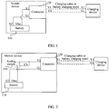
- FIG. 1 is a schematic structural diagram of the mobile device according to this embodiment of the present invention.
- An implementation body of the embodiment shown in FIG. 1 is the mobile device.
- the mobile device includes the following components: a battery 110 and a connector 120.
- the connector includes a charging pin V1 and a ground pin G1.
- the charging pin When the charging pin establishes a connection to an output pin of a charging device by using a charging cable or a battery charging stand, the charging pin receives a first current signal transmitted by the output pin of the charging device, and transmits the first current signal to an anode pin of the battery, so as to charge the battery.
- one end of the charging pin of the connector is connected to the anode pin of the battery, and the other end is connected to the output pin of the charging device by using the charging cable or the battery charging stand.
- the charging cable is specifically a current signal that can endure a high voltage and a high current.
- the charging cable can specifically endure a high-current signal of 25 V/5 A, and can further endure a high-current signal that exceeds 25 V/5 A in an actual application.
- the charging device is a charging device that provides electric energy, includes a charging circuit and may be connected to a common power supply.
- the charging circuit in the charging device can provide a high-current signal, and the first current signal may be specifically a high-current signal of 5 A.
- the mobile device in this embodiment of the present invention may directly receive, by using the connector, a high current provided by the charging device, so as to shorten a charging time.
- a charging circuit that provides a high current does not exist in the mobile device, but exists in the charging device, which makes the mobile device only receive a high current, so as to reduce a heat loss as much as possible.
- the mobile device is connected to the charging device by using a charging cable or a battery charging stand, and receives a high current transmitted by the charging device, so as to charge a battery of the mobile device.
- a charging circuit that provides a high current is not included in the mobile device, but exists in the charging device, which makes the mobile device only receive a high current, so as to reduce a heat loss of the mobile device as much as possible.
- the mobile device is also made to adapt to a charging mode in which a supply voltage and a supply current have been increased, and a solution in the prior art is also enriched.
- the mobile device further includes an analog switch 210.
- the analog switch in FIG. 2 may be a single-pole single-throw switch, and may be specifically implemented by using a field effect transistor.
- a lead EN is led from the charging pin VI of the connector, and the lead EN is connected to a switch joint of the analog switch.
- the charging pin VI establishes a connection to an output pin VI of a charging device by using a charging cable or a battery charging stand
- a voltage of the lead EN changes, which triggers the analog switch to close, so as to connect the anode pin of the battery to the charging pin V1 of the connector.
- the analog switch 210 When the connector is not connected to a charging device, the analog switch 210 is in a disconnected state, and the ground pin G1 of the connector is connected to a ground pin G2 of the battery.
- the charging pin receives a first current signal transmitted by the output pin of the charging device, and transmits the first current signal to the anode pin of the battery by using the analog switch, so as to charge the battery.
- the analog switch 210 is added.
- the charging pin establishes a connection to the output pin of the charging device by using a charging cable or a battery charging stand
- the analog switch is triggered to connect the anode pin of the battery to the charging pin, which can prevent electric leakage of the connector when charging is not performed.
- the lead EN is led from the charging pin V1 of the connector, and the lead EN is connected to the switch joint of the analog switch. If the voltage of the lead EN jumps from a low electrical level to a high electrical level, it indicates that the charging pin VI has established a connection to the output pin VI of the charging device by using the charging cable or the battery charging stand; if the voltage of the lead EN jumps from a high electrical level to a low electrical level, it indicates that the charging pin VI has been disconnected from the output pin V1 of the charging device.
- the charging pin VI establishes a connection to an output pin VI of an external charging device by using a charging cable or a battery charging stand, so that the charging pin VI receives a first current signal, so as to charge the battery.
- the mobile device further includes a charging circuit 310 and a universal serial bus USB port 320.
- the analog switch in FIG. 3 is a single-pole double-throw switch, and is specifically implemented by using a field effect transistor.
- the anode pin Vbat of the battery is connected to an output pin V2 of the charging circuit by using the analog switch, an input pin V3 of the charging circuit is connected to the USB port, a ground pin G3 of the charging circuit, the ground pin G2 of the battery and the ground pin G1 of the connector are connected to each other, and the charging pin V1 of the connector hangs in the air; one end of a voltage converting circuit is connected to the charging pin VI, and the other end is connected to a voltage pin Vdet of a controller.
- the charging circuit and the universal serial bus USB port are added.
- the charging circuit and the USB port when the charging pin VI is disconnected from an output pin VI of the charging device, the battery may still be charged by using the USB port, and data exchange with another mobile device may also be implemented by using the USB port.
- the analog switch disconnects the anode pin Vbat of the battery from the charging pin VI, and the output pin V2 of the charging circuit is connected to the anode pin Vbat of the battery by using the analog switch.
- the input pin V3 of the charging circuit is connected to the USB port, receives a second current signal transmitted by the USB port, and transmits the second current signal to the anode pin Vbat of the battery by using the output pin V2 of the charging circuit and the analog switch, so as to charge the battery.
- the charging circuit 310 in the mobile device is configured to provide a direct current signal required by the battery, and specifically, a charging circuit in an existing mobile device may be used. In order not to make the mobile device generate an unendurable heat loss due to charging with a high current, the charging circuit in the mobile device is set to provide a low-current signal.
- the mobile device (such as a mobile phone or a tablet computer) may further be connected to another mobile device (such as a desktop computer or a notebook computer) by using the USB port.
- the another mobile device may be connected to a common power supply, so as to provide electric energy for the mobile device in this embodiment of the present invention.
- the second current signal may be specifically a low-current signal of 2 A.
- the charging device in this embodiment includes a charging circuit, where the charging circuit can provide a high-current signal, for example, a current signal of 5 A.
- the mobile device in this embodiment of the present invention may directly receive, by using the connector, a high current provided by the charging device, so as to shorten a charging time.
- a charging circuit that provides a high current does not exist in the mobile device, but exists in the charging device, which makes the mobile device only receive a high current, so as to reduce a heat loss as much as possible.
- the charging circuit in the mobile device is a charging circuit that can maintain the low-current signal of 2 A. Therefore, a heat loss of the mobile device can be further reduced.
- the lead EN is led from the charging pin VI of the connector, and the lead EN is connected to the switch joint of the analog switch. If the voltage of the lead EN jumps from a low electrical level to a high electrical level, it indicates that the charging pin VI has established a connection to the output pin VI of the charging device by using the charging cable or the battery charging stand; if the voltage of the lead EN jumps from a high electrical level to a low electrical level, it indicates that the charging pin VI has been disconnected from the output pin VI of the charging device.
- the charging pin VI establishes a connection to an output pin VI of an external charging device by using a charging cable or a battery charging stand, so that the charging pin VI receives a first current signal, so as to charge the battery.
- the mobile device further includes a controller 410 and a voltage converting circuit 420, as shown in FIG. 4 .
- the voltage converting circuit is configured to: when the charging pin VI establishes a connection to an output pin of a charging device by using a charging cable or a battery charging stand, detect a voltage of the charging pin, convert the voltage and then transmit a converted voltage to the controller, so that the controller determines that the mobile device established a connection to the charging device.
- the voltage converting circuit adjusts a detected voltage value of the charging pin to a voltage value that can be endured by the controller.
- the voltage of the charging pin is a voltage of approximately 10 V, and the voltage that can be endured by the controller is 2 V; then, the voltage converting circuit adjusts the voltage of the charging pin to a voltage of 2 V that can be endured by the controller, so that the controller determines that the mobile device has established a connection to the charging device.
- the controller further includes a bus port
- the connector further includes a single-wire or multi-wire bus pin
- the charging device includes a bus port (not clearly shown in FIG. 4 ).
- the bus port of the controller is connected to the single-wire or multi-wire pin by using a bus, and the single-wire or multi-wire bus pin of the connector is also connected to a bus pin of the charging device by using the bus.
- the bus port of the controller is connected to the bus port of the charging device by using the single-wire or multi-wire bus pin of the connector.
- the bus is configured to transmit bus data or a control signal generated by the controller, so that the pin corresponding to the charging device adjusts an output first current signal after receiving the bus data or the control signal.
- the bus may be an inter-integrated circuit I2C bus
- the single-wire or multi-wire bus pin included in the connector is an I2C data pin I2C-DATA and an I2C clock pin I2C-CLK, as shown in FIG. 1 .
- the I2C data pin I2C-DATA is connected to the bus port of the controller, and is configured to transmit I2C data or a control signal generated by the controller;
- the I2C clock pin I2C-CLK is connected to the bus port of the controller, and is configured to transmit an I2C clock signal generated by the controller, so that the bus port corresponding to the charging device adjusts the output first current signal after receiving the I2C data or the control signal, and the I2C clock signal.
- the mobile device transmits, by using the I2C data pin I2C-DATA and the I2C clock pin I2C-CLK of the connector and the I2C bus, the I2C data or the control signal, and the I2C clock signal to the bus port corresponding to the charging device.
- the mobile device After the mobile device establishes a connection to the charging device by using a charging cable, charging is performed.
- the controller may notify the charging device of a required first current signal by transmitting I2C data or a control signal, and an I2C clock signal to the charging device, so that the charging device adjusts the output first current signal according to the I2C data or the control signal, and the I2C clock signal that are received by the corresponding port.
- bus port of the controller and the bus pin of the connector by using an I2C bus as an example.
- a connection between the bus port of the controller and the single-wire or multi-wire bus pin of the connector is not limited to use of an I2C bus, and an SPI bus or the like may also be used.
- the ground pin G1 of the connector is connected to a first ground pin G1 of the charging device by using the charging cable or the battery charging stand, and the ground pin G1, the ground pin G2 of the battery and the ground pin G3 of the charging circuit are connected to each other.
- the connector is specifically a multi-pin port, a multi-contact port, or a port multiplexed with the USB port by using the analog switch.
- the connector in the mobile device provided in this embodiment of the present invention may be formed by multiple types of ports, such as a multi-pin port, a multi-contact port, or a port multiplexed with the USB port by using the analog switch.
- a multi-pin port such as a multi-pin port, a multi-contact port, or a port multiplexed with the USB port by using the analog switch.
- an analog switch and a USB port are multiplexed to serve as a connector, as shown in FIG. 5 .
- the analog switch and the USB port are multiplexed, so as to implement functions of the connector in the foregoing embodiment.
- a charging process implemented by the mobile device is as follows: When the mobile device does not establish a connection to a charging device, the analog switch is connected to the charging circuit of the mobile device by default.
- the lead EN is led from the voltage pin of the controller, and the lead EN is connected to the switch joint of the analog switch.
- the analog switch remains connected to the charging circuit when the controller detects, by using a USB ID pin, that the mobile device is connected to a computer or another USB device by using a USB cable to perform USB charging; when the controller detects, by using the USB ID pin, that the mobile device is charged by using the charging device, a voltage of the lead EN jumps from a low electrical level to a high electrical level, and the analog switch is disconnected from the charging circuit, and is connected to a Vbat pin of the battery through switching, so as to complete charging of the battery.
- FIG. 5 is only an example for implementing the functions of the connector by using another method, and no limitation is constituted thereto in an actual application.
- FIG. 6 is a schematic structural diagram of the charging device according to this embodiment of the present invention.
- An implementation body of the embodiment shown in FIG. 6 is the charging device.
- the charging device includes the following parts: a switch charger module 610 and a charging circuit 620.
- an output pin V3 and a ground pin G3 of the switch charger module are respectively connected to an input pin V2 and a second ground pin G2 of the charging circuit
- an output pin VI of the charging circuit is connected to a charging pin VI of a mobile device by using a charging cable or a battery charging stand
- a first ground pin G1 of the charging circuit is connected to a first ground pin G1 of the mobile device by using a charging cable or a battery charging stand.
- the charging circuit includes the output pin VI and the input pin V2.
- the input pin V2 is connected to the output pin V3 of the switch charger module, and is configured to receive a first current signal transmitted by the output pin V3 of the switch charger module.
- the output pin V1 establishes a connection to the charging pin V1 of the mobile device by using a charging cable or a battery charging stand, so as to use the first current signal to charge a battery of the mobile device.
- the output pin VI of the charging circuit establishes a connection to the charging pin VI of the mobile device by using a charging cable or a battery charging stand
- the output pin VI transmits a carried voltage to the charging pin VI, which makes a voltage of a lead EN connected to the charging pin V1 jump, so as to connect an analog switch in the mobile device to the charging pin VI, so that the first current signal is transmitted to an anode pin Vbat of the battery by using the analog switch, so as to charge a power supply in the mobile device.
- the charging cable is specifically a current signal that can endure a high voltage and a high current.
- the charging cable can specifically endure a high-current signal of 25 V/5 A, and can further endure a high-current signal that exceeds 25 V/5 A in an actual application.
- the switch charger module in this embodiment of the present invention is configured to: connect to a power supply, receive an alternating current signal transmitted by the power supply, convert the alternating current signal into a direct current signal, and transmit the direct current signal to the charging circuit.
- the charging circuit is configured to: receive the direct current signal, convert the received direct current signal into a direct current signal required by the battery of the mobile device, and transmit, by using a charging cable or a battery charging stand, the direct current signal required by the battery to the mobile device, where the direct current signal that is required by the battery and that is transmitted to the mobile device is a first current signal.
- the switch charger module is connected to a common power supply, and receives an alternating current signal (for example, an alternating current of 220 V) transmitted by the power supply.
- the switch charger module converts the alternating current signal into a direct current signal (for example, a direct current of 110 V), and transmits the direct current signal, which is obtained after conversion, to the input pin V2 of the charging circuit by using the output pin V3.
- the input pin V2 of the charging circuit receives the direct current signal transmitted by the switch charger module, converts, according to a charge curve of the battery of the mobile device, the direct current signal into a direct current signal required by the battery, and transmits, by using the output pin VI of the charging circuit and a charging cable or a battery charging stand, the direct current signal required by the battery to the charging pin VI of the mobile device.
- a charge curve of a battery is a characteristic curve of charging of the battery.
- the battery when the battery is empty (a battery level is zero), in this case, the battery can receive only a low current for charging, and therefore, the charging circuit provides a current signal of a low current for the battery according to the charge curve of the battery.
- the charging circuit When there is a certain amount of electricity in the battery (the battery level is 20% of a total battery capacity), in this case, the battery can receive a high current for charging, and therefore, the charging circuit provides a current signal of a high current for the battery according to the charge curve of the battery.
- the charging device is a charging device that provides electric energy and may be connected to a common power supply.
- the first current signal may be specifically a high-current signal of 5 A.
- the charging circuit that provides a high-current signal is disposed in the charging circuit; therefore, the mobile device may directly receive, by using a connector, a high current provided by the charging device, so as to shorten a charging time, so that a heat loss is reduced as much as possible even if a high current is received.
- the charging circuit further includes a bus port.
- the bus port of the charging circuit is connected to a bus pin of the connector in the mobile device, and is configured to receive bus data or a control signal transmitted by the mobile device.
- the charging circuit is further configured to adjust the first current signal according to the bus data or the control signal.
- the bus port of the charging circuit when a bus is an I2C bus, the bus port of the charging circuit includes an I2C data pin I2C-DATA and an I2C clock pin I2C-CLK.
- the I2C data pin I2C-DATA in the charging circuit and an I2C data pin I2C-DATA of the connector in the mobile device are configured to receive I2C data or a control signal generated by a controller in the mobile device.
- the I2C clock pin I2C-CLK in the charging circuit is connected to an I2C clock pin I2C-CLK of the connector in the mobile device, and is configured to receive an I2C clock signal generated by the controller in the mobile device.
- the charging circuit is further configured to adjust the first current signal according to the I2C data or the control signal, and the I2C clock signal.
- the mobile device transmits the I2C data or the control signal, and the I2C clock signal to the charging device by using the I2C data pin I2C-DATA and the I2C clock pin I2C-CLK of the connector and the I2C bus.
- the mobile device After the mobile device establishes a physical connection to the charging device by using a charging cable, charging is performed.
- the controller may notify the charging device of a required first current signal by transmitting I2C data or a control signal, and an I2C clock signal to the charging device, so that the charging device adjusts the output first current signal according to the I2C data or the control signal, and the I2C clock signal that are received, and then transmits an adjusted first current signal to an anode pin VI of the connector in the mobile device by reusing the charging cable.
- a type of a bus is not limited to an I2C bus, and may also be an SPI bus or the like.
- the charging circuit further includes the first ground pin G1 and the second ground pin G2.
- the first ground pin G1 is connected to the ground pin G1 of the mobile device by using a charging cable or a battery charging stand.
- the second ground pin G2 is connected to the ground pin G3 of the switch charger module.
- the charging circuit is specifically a switch charging circuit or a linear charging circuit.
- a charging circuit that can provide a high current is disposed in the charging device, so as to reduce a heat loss of a mobile device.
- the charging circuit may be specifically set as a switch charging circuit or a linear charging circuit, so as to reduce a heat loss of the charging device.
- the switch charging circuit or the linear charging circuit is a circuit well known to a person skilled in the art, and therefore, details are not described herein again.
- a charging circuit that can provide a high current is added in the charging device, to transmit a high current to a mobile device by using a charging cable, which makes the mobile device only receive a high current, so as to reduce a heat loss of the mobile device as much as possible. Further, a heat generation problem during a process of charging a mobile device in the prior art is resolved, the mobile device is also made to adapt to a charging mode in which a supply voltage and a supply current have been increased, and a solution in the prior art is also enriched.
- a mobile device and a charging device are separately used as implementation bodies to briefly describe charging processes. Further, the charging processes described in the foregoing embodiments may be completed by using a schematic diagram of a connection system of a mobile device and a charging device shown in FIG. 7 . As shown in FIG. 7 , the mobile terminal includes the foregoing multiple components, and a specific charging process is as follows:
- a charging pin VI establishes a connection to an output pin VI of the charging device by using a charging cable or a battery charging stand
- an analog switch connects an anode pin Vbat of a battery to the charging pin VI; the charging pin VI receives a first current signal transmitted by the output pin VI of the charging device, and transmits the first current signal to the anode pin Vbat of the battery by using the analog switch, so as to charge the battery.
- the mobile device may further perform communication exchange with the charging device by using an I2C bus, and the mobile device transmits an I2C data signal and an I2C control signal to the charging device by using the I2C bus, so that the charging device adjusts an output current signal.
- the foregoing describes a charging process performed after a mobile device establishes a connection to a charging device by using a charging cable.
- the mobile device may receive a second current signal from a USB port by using a charging circuit of the mobile device, so as to charge a battery.
- Charging a battery by using a USB port is the prior art; therefore, details are not described herein again.
- FIG. 8 is a flowchart of the charging method according to this embodiment of the present invention.
- the charging method provided in this embodiment of the present invention is based on the mobile device and the charging device that are described in the foregoing embodiments.
- the charging method specifically includes the following steps:
- Step 810 When a charging pin of a connector establishes a connection to an output pin of a charging device by using a charging cable or a battery charging stand, the charging pin receives a first current signal transmitted by the output pin of the charging device.
- one end of the charging pin of the connector is connected to an anode pin of a battery, and the other end is connected to the output pin of the charging device by using a charging cable or a battery charging stand.
- the charging cable is specifically a current signal that can endure a high voltage and a high current.
- the charging cable can specifically endure a high-current signal of 25 V/5 A, and can further endure a high-current signal that exceeds 25 V/5 A in an actual application.
- the charging device is a charging device that provides electric energy and may be connected to a common power supply.
- the first current signal may be specifically a high-current signal of 5 A.
- Step 820 The charging pin transmits the first current signal to the anode pin of the battery, so as to charge the battery.
- the charging pin of the connector is connected to the anode pin of the battery. After the charging pin receives the first current signal output by the output pin of the charging device, the charging pin transmits the first current signal to the anode pin of the battery, so as to charge the battery.
- a mobile device in this embodiment of the present invention may directly receive, by using a connector, a high current provided by a charging device, so as to shorten a charging time.
- a charging circuit that provides a high current does not exist in the mobile device, but exists in the charging device, which makes the mobile device only receive a high current, so as to reduce a heat loss as much as possible.
- an embodiment of the present invention further provides another charging method.
- An analog switch is disposed between the anode pin of the battery and the charging pin.
- the charging pin of the connector establishes a connection to the output pin of the charging device by using a charging cable or a battery charging stand
- the analog switch connects the anode pin of the battery to the charging pin.
- the charging cable is specifically a current signal that can endure a high voltage and a high current.
- the charging cable can specifically endure a high-current signal of 25 V/5 A, and can further endure a high-current signal that exceeds 25 V/5 A in an actual application.
- the charging pin receives the first current signal transmitted by the output pin of the charging device.
- the charging pin receives, by using a charging cable or a battery charging stand, the first current signal output by the output pin of the charging device.
- the charging device is a charging device that provides electric energy and may be connected to a common power supply.
- the first current signal may be specifically a high-current signal of 5 A.
- the charging pin transmits the first current signal to the anode pin of the battery by using the analog switch, so as to charge the battery.
- the analog switch connects the charging pin of the connector to the anode pin of the battery; therefore, after receiving the first current signal output by the output pin of the charging device, the charging pin transmits the first current signal to the anode pin of the battery by using the analog switch, so as to charge the battery.
- a mobile device in this embodiment of the present invention may directly receive, by using a connector, a high current provided by a charging device, so as to shorten a charging time.
- a charging circuit that provides a high current does not exist in the mobile device, but exists in the charging device, which makes the mobile device only receive a high current, so as to reduce a heat loss as much as possible.
- this embodiment of the present invention further includes a step in which when the charging pin of the connector is disconnected from the output pin of the charging device, the battery may still be charged by using a USB port.
- the mobile device may also perform data exchange with another mobile device by using the USB port.
- the analog switch disconnects the anode pin of the battery from the charging pin, and an output pin of the charging circuit is connected to the anode pin of the battery by using the analog switch.
- An input pin of the charging circuit receives a second current signal by using the USB port.
- the input pin of the charging circuit is connected to the USB port and receives the second current signal by using the USB port.
- the mobile device (such as a mobile phone or a tablet computer) may further be connected to another mobile device (such as a desktop computer or a notebook computer) by using the USB port.
- the another mobile device may be connected to a common power supply, so as to provide electric energy for the mobile device in this embodiment of the present invention.
- the second current signal may be specifically a low-current signal of 2 A.
- the input pin of the charging circuit transmits the second current signal to the anode pin of the battery by using the output pin of the charging circuit and the analog switch, so as to charge the battery.
- the output pin of the charging circuit is connected to a voltage pin of the battery by using the analog switch, and the input pin of the charging circuit is connected to the USB port; therefore, after receiving the second current signal by using the USB port, the input pin of the charging circuit transmits the second current signal to the battery by using the output pin of the charging device and the analog switch, so as to charge the battery.
- a mobile device in this embodiment of the present invention may directly receive, by using a connector, a high current provided by a charging device, so as to shorten a charging time.
- a charging circuit that provides a high current does not exist in the mobile device, but exists in the charging device, which makes the mobile device only receive a high current, so as to reduce a heat loss as much as possible.
- the charging circuit in the mobile device is a charging circuit that can maintain the low-current signal of 2 A. Therefore, a heat loss of the mobile device can be further reduced.
- this embodiment of the present invention further includes a step of performing exchange communication by the mobile device with the charging device by using a bus.
- the controller generates bus data or a control signal.
- step 810 and step 820 after the mobile device establishes a connection to the charging device by using a charging cable, charging is performed.
- the controller determines that a first current signal provided by the charging device is so high that the mobile device cannot endure, the controller generates bus data or a control signal.
- the controller transmits the bus data or the control signal to a bus port of the charging device by using a bus port and a single-wire or multi-wire bus pin of the connector, so that the charging device adjusts an output first current signal.
- a mobile device is connected to a charging device by using a charging cable, and receives a high current transmitted by the charging device, so as to charge a battery of the mobile device.
- a charging circuit that provides a high current is not included in the mobile device, but exists in the charging device, which makes the mobile device only receive a high current, so as to reduce a heat loss of the mobile device as much as possible.
- the mobile device is also made to adapt to a charging mode in which a supply voltage and a supply current have been increased, and a solution in the prior art is also enriched.
- Steps of methods or algorithms described in the embodiments disclosed in this specification may be implemented by hardware, a software module executed by a processor, or a combination thereof.
- the software module may reside in a random access memory (RAM), a memory, a read-only memory (ROM), an electrically programmable ROM, an electrically erasable programmable ROM, a register, a hard disk, a removable disk, a CD-ROM, or any other form of storage medium known in the art.
- Embodiment 1 A mobile device, wherein the mobile device comprises a battery and a connector, wherein the connector comprises a charging pin and a ground pin; and when the charging pin establishes a connection to an output pin of a charging device by using a charging cable or a battery charging stand, the charging pin receives a first current signal transmitted by the output pin of the charging device, and transmits the first current signal to an anode pin of the battery, so as to charge the battery.
- Embodiment 2 The mobile device according to embodiment 1, wherein the mobile device further comprises an analog switch; when the charging pin establishes a connection to the output pin of the charging device by using a charging cable or a battery charging stand, the analog switch connects the anode pin of the battery to the charging pin; and the charging pin receives the first current signal transmitted by the output pin of the charging device, and transmits the first current signal to the anode pin of the battery by using the analog switch, so as to charge the battery.
- the analog switch when the charging pin establishes a connection to the output pin of the charging device by using a charging cable or a battery charging stand, the analog switch connects the anode pin of the battery to the charging pin; and the charging pin receives the first current signal transmitted by the output pin of the charging device, and transmits the first current signal to the anode pin of the battery by using the analog switch, so as to charge the battery.
- Embodiment 3 The mobile device according to embodiment 2, wherein the mobile device further comprises a charging circuit and a universal serial bus USB port; when the charging pin is disconnected from the output pin of the charging device, the analog switch disconnects the anode pin of the battery from the charging pin, and an output pin of the charging circuit is connected to the anode pin of the battery by using the analog switch; and an input pin of the charging circuit is connected to the USB port, receives a second current signal transmitted by the USB port, and transmits the second current signal to the anode pin of the battery by using the output pin of the charging circuit and the analog switch, so as to charge the battery.
- the analog switch disconnects the anode pin of the battery from the charging pin
- an output pin of the charging circuit is connected to the anode pin of the battery by using the analog switch
- an input pin of the charging circuit is connected to the USB port, receives a second current signal transmitted by the USB port, and transmits the second current signal to the anode pin of the battery by using the output pin of the charging circuit and
- Embodiment 4 The mobile device according to any one of embodiments 1 to 3, wherein the mobile device further comprises a controller and a voltage converting circuit, wherein with one end connected to the charging pin, and the other end connected to the controller, the voltage converting circuit is configured to: when the charging pin establishes a connection to the output pin of the charging device by using a charging cable or a battery charging stand, convert a voltage of the charging pin and then transmit a converted voltage to the controller.
- Embodiment 5 The mobile device according to embodiment 4, wherein the controller further comprises a bus port, and the connector further comprises a single-wire or multi-wire bus pin, wherein the bus port is connected to the single-wire or multi-wire bus pin of the connector by using a bus, and is configured to transmit bus data or a control signal generated by the controller, so that the charging device adjusts the output first current signal after receiving the bus data or the control signal.
- Embodiment 6 The mobile device according to any one of embodiments 1 to 5, wherein the ground pin is connected to a first ground pin of the charging device by using the charging cable or the battery charging stand; and the ground pin, a ground pin of the battery and a ground pin of the charging circuit are connected to each other.
- Embodiment 7 The mobile device according to any one of embodiments 1 to 6, wherein the connector is specifically a multi-pin port, a multi-contact port, or a port multiplexed with the USB port by using the analog switch.
- Embodiment 8 A charging device, wherein the charging device comprises a switch charger module and a charging circuit, wherein the charging circuit comprises an input pin and an output pin; the input pin is connected to an output pin of the switch charger module, and is configured to receive a first current signal transmitted by the output pin of the switch charger module; and the output pin establishes a connection to a charging pin of a mobile device by using a charging cable or a battery charging stand, so as to use the first current signal to charge a battery of the mobile device.
- the charging device comprises a switch charger module and a charging circuit
- the charging circuit comprises an input pin and an output pin
- the input pin is connected to an output pin of the switch charger module, and is configured to receive a first current signal transmitted by the output pin of the switch charger module
- the output pin establishes a connection to a charging pin of a mobile device by using a charging cable or a battery charging stand, so as to use the first current signal to charge a battery of the mobile device.
- Embodiment 9 The charging device according to embodiment 8, wherein the charging circuit further comprises a bus port, wherein the bus port is connected to a single-wire or multi-wire bus pin of a connector in the mobile device by using a bus, and is configured to receive bus data or a control signal transmitted by the mobile device; and the charging circuit is further configured to adjust the first current signal according to the bus data or the control signal.
- the bus port is connected to a single-wire or multi-wire bus pin of a connector in the mobile device by using a bus, and is configured to receive bus data or a control signal transmitted by the mobile device; and the charging circuit is further configured to adjust the first current signal according to the bus data or the control signal.
- Embodiment 10 The charging device according to embodiment 8 or 9, wherein the charging circuit further comprises a first ground pin and a second ground pin; wherein the first ground pin is connected to a ground pin of the mobile device by using the charging cable or the battery charging stand; and the second ground pin is connected to a ground pin of the switch charger module.
- Embodiment 11 The charging device according to any one of embodiments 8 to 10, wherein the charging circuit is specifically a switch charging circuit or a linear charging circuit.
- Embodiment 12 A charging method, wherein the method comprises:
- Embodiment 13 The charging method according to embodiment 12, wherein after the receiving, by a charging pin of a connector when the charging pin establishes a connection to an output pin of a charging device by using a charging cable or a battery charging stand, a first current signal transmitted by the output pin of the charging device, and before the transmitting, by the charging pin, the first current signal to an anode pin of the battery, the method further comprises: connecting, by an analog switch, the anode pin of the battery to the charging pin.
- Embodiment 14 The charging method according to embodiment 13, wherein the method further comprises:
- Embodiment 15 The charging method according to any one of embodiments 12 to 14, wherein the method further comprises:
- Embodiment 16 A charging system, wherein the charging system comprises the mobile device according to any one of embodiments 1 to 7 and the charging device according to any one of embodiments 8 to 11.
Applications Claiming Priority (3)
| Application Number | Priority Date | Filing Date | Title |
|---|---|---|---|
| CN201310018595.9A CN103107575B (zh) | 2013-01-18 | 2013-01-18 | 充电方法、移动设备、充电设备与充电系统 |
| PCT/CN2014/070354 WO2014110995A1 (zh) | 2013-01-18 | 2014-01-09 | 充电方法、移动设备、充电设备与充电系统 |
| EP14741179.7A EP2942853B1 (de) | 2013-01-18 | 2014-01-09 | Ladeverfahren, mobile vorrichtung, ladevorrichtung und ladesystem |
Related Parent Applications (2)
| Application Number | Title | Priority Date | Filing Date |
|---|---|---|---|
| EP14741179.7A Division EP2942853B1 (de) | 2013-01-18 | 2014-01-09 | Ladeverfahren, mobile vorrichtung, ladevorrichtung und ladesystem |
| EP14741179.7A Division-Into EP2942853B1 (de) | 2013-01-18 | 2014-01-09 | Ladeverfahren, mobile vorrichtung, ladevorrichtung und ladesystem |
Publications (2)
| Publication Number | Publication Date |
|---|---|
| EP3432441A1 true EP3432441A1 (de) | 2019-01-23 |
| EP3432441B1 EP3432441B1 (de) | 2023-05-31 |
Family
ID=48315225
Family Applications (2)
| Application Number | Title | Priority Date | Filing Date |
|---|---|---|---|
| EP18172989.8A Active EP3432441B1 (de) | 2013-01-18 | 2014-01-09 | Ladeverfahren, mobile vorrichtung, ladevorrichtung und ladesystem |
| EP14741179.7A Active EP2942853B1 (de) | 2013-01-18 | 2014-01-09 | Ladeverfahren, mobile vorrichtung, ladevorrichtung und ladesystem |
Family Applications After (1)
| Application Number | Title | Priority Date | Filing Date |
|---|---|---|---|
| EP14741179.7A Active EP2942853B1 (de) | 2013-01-18 | 2014-01-09 | Ladeverfahren, mobile vorrichtung, ladevorrichtung und ladesystem |
Country Status (12)
| Country | Link |
|---|---|
| US (3) | US9991725B2 (de) |
| EP (2) | EP3432441B1 (de) |
| JP (2) | JP6452162B2 (de) |
| KR (2) | KR101933066B1 (de) |
| CN (1) | CN103107575B (de) |
| AU (2) | AU2014207189C1 (de) |
| CA (1) | CA2908514C (de) |
| ES (2) | ES2688581T3 (de) |
| RU (2) | RU2633710C2 (de) |
| SG (2) | SG11201508298WA (de) |
| WO (1) | WO2014110995A1 (de) |
| ZA (2) | ZA201507519B (de) |
Families Citing this family (21)
| Publication number | Priority date | Publication date | Assignee | Title |
|---|---|---|---|---|
| CN103107575B (zh) * | 2013-01-18 | 2015-07-29 | 华为终端有限公司 | 充电方法、移动设备、充电设备与充电系统 |
| US11797469B2 (en) | 2013-05-07 | 2023-10-24 | Snap-On Incorporated | Method and system of using USB user interface in electronic torque wrench |
| CN107069853B (zh) * | 2014-01-28 | 2019-04-26 | Oppo广东移动通信有限公司 | 启动充电的检测电路和方法 |
| CN106300456B (zh) * | 2015-05-18 | 2021-04-13 | 中兴通讯股份有限公司 | 一种实现充电的受电装置和供电装置 |
| EP3985835A1 (de) * | 2015-09-22 | 2022-04-20 | Guangdong Oppo Mobile Telecommunications Corp., Ltd. | Ladesteuerungsverfahren und -vorrichtung sowie elektronische vorrichtung |
| CN105281403A (zh) * | 2015-10-19 | 2016-01-27 | 杭州德澜科技有限公司 | 一种使用usb接口通信的智能插座 |
| CN105280149B (zh) * | 2015-11-11 | 2017-11-17 | 深圳市华星光电技术有限公司 | 一种Mura补偿数据写入装置及方法 |
| US10283975B1 (en) * | 2016-03-28 | 2019-05-07 | Amazon Technologies, Inc. | Smart diagnostics for hot-pluggable battery systems |
| CN107231012B (zh) | 2016-04-08 | 2019-05-24 | 华为技术有限公司 | 一种快速充电的方法、终端、充电器和系统 |
| CN105762891A (zh) * | 2016-04-28 | 2016-07-13 | 行科技有限责任公司 | 一种智能移动终端的充电电路及其方法 |
| CN106451613B (zh) * | 2016-09-21 | 2019-05-24 | 奇酷互联网络科技(深圳)有限公司 | 移动装置及其充电方法 |
| WO2018068243A1 (zh) | 2016-10-12 | 2018-04-19 | 广东欧珀移动通信有限公司 | 移动终端 |
| US11056896B2 (en) | 2016-10-12 | 2021-07-06 | Guangdong Oppo Mobile Telecommunications Corp., Ltd. | Terminal and device |
| WO2018072083A1 (zh) * | 2016-10-18 | 2018-04-26 | 深圳达闼科技控股有限公司 | 一种充电限流方法、装置及电子设备 |
| ES2865855T3 (es) | 2017-04-13 | 2021-10-18 | Guangdong Oppo Mobile Telecommunications Corp Ltd | Dispositivo a ser cargado y método de carga |
| CN109068220B (zh) * | 2018-09-03 | 2020-11-03 | 歌尔股份有限公司 | 耳机、耳机充电盒和耳机套装 |
| CN110970954B (zh) * | 2018-09-29 | 2021-06-15 | Oppo广东移动通信有限公司 | 充电控制方法、装置、存储介质及分体式电子设备 |
| JP7336264B2 (ja) * | 2019-05-29 | 2023-08-31 | 株式会社マキタ | バッテリパック |
| AU2021200856B2 (en) * | 2020-02-28 | 2022-12-01 | Snap-On Incorporated | Method and system of using usb user interface in electronic torque wrench |
| CN113547955B (zh) * | 2020-04-23 | 2023-06-16 | 宁德时代新能源科技股份有限公司 | 电池的充电控制方法、装置、电池管理系统和介质 |
| CN114123434B (zh) * | 2022-01-27 | 2022-04-15 | 深圳市高端无人机有限公司 | 电源电路及电子设备 |
Citations (5)
| Publication number | Priority date | Publication date | Assignee | Title |
|---|---|---|---|---|
| US20050174094A1 (en) * | 2004-02-11 | 2005-08-11 | Research In Motion Limited, A Canadian Corporation | Battery charger for portable devices and related methods |
| US20070120531A1 (en) * | 2005-11-28 | 2007-05-31 | Lg Electronics Inc. | Charging Control Apparatus and Method of Mobile Terminal |
| US20090174366A1 (en) * | 2008-01-09 | 2009-07-09 | Freescale Semiconductor, Inc. | Multiple Function Switching Regulator for Use in Mobile Electronic Devices |
| US20100060233A1 (en) * | 2008-09-08 | 2010-03-11 | Nien-Hui Kung | Charger with USB detection |
| EP2424067A1 (de) * | 2010-08-26 | 2012-02-29 | ST-Ericsson SA | Leistungsverwaltungsschaltung für ein tragbares elektronisches Gerät mit USB-Funktionalität und Verfahren dafür |
Family Cites Families (36)
| Publication number | Priority date | Publication date | Assignee | Title |
|---|---|---|---|---|
| CN2140581Y (zh) | 1992-11-24 | 1993-08-18 | 李知非 | 智能超快速充电器 |
| CN2192974Y (zh) | 1994-06-22 | 1995-03-22 | 李知非 | 家用智能超快速充电/治疗器 |
| US5672952A (en) | 1996-07-01 | 1997-09-30 | Analog Devices, Inc. | Controller for battery charger with reduced reverse leakage current |
| JP2001251771A (ja) * | 2000-03-07 | 2001-09-14 | Hitachi Maxell Ltd | 充電電池あるいは充電電池パック、これらのいずれかを有する電子装置 |
| KR100539530B1 (ko) | 2002-02-01 | 2005-12-30 | 엘지전자 주식회사 | 일체형 무선 가입자 망 단말기 |
| KR200275514Y1 (ko) * | 2002-02-15 | 2002-05-11 | 신형범 | 충전지를 내장한 휴대용 충전장치 |
| CN2606979Y (zh) * | 2002-10-29 | 2004-03-17 | 联想(北京)有限公司 | 新型便携式设备智能充电装置 |
| KR100487622B1 (ko) * | 2003-04-25 | 2005-05-03 | 엘지전자 주식회사 | 배터리 충전전류 가변 장치 및 그 방법 |
| KR100965876B1 (ko) | 2003-06-03 | 2010-06-24 | 삼성전자주식회사 | Usb를 이용한 배터리 충전장치 및 이를 구비하는디지털 카메라 |
| JP4131844B2 (ja) * | 2003-09-10 | 2008-08-13 | 京セラ株式会社 | 携帯端末 |
| JP2005237155A (ja) | 2004-02-20 | 2005-09-02 | Macnica Inc | 複数電圧仕様対応のバッテリー充電器、バッテリー充電システム、及びバッテリーユニット |
| KR100585763B1 (ko) * | 2004-05-31 | 2006-06-07 | 엘지전자 주식회사 | 이동단말기 및 그의 배터리 충전방법 |
| KR100622918B1 (ko) * | 2005-02-01 | 2006-09-14 | 엘지전자 주식회사 | 이동통신단말기의 배터리 충전전류 자가보상장치 및 이를이용한 보상방법 |
| JP4350665B2 (ja) | 2005-02-25 | 2009-10-21 | 京セラ株式会社 | 電子機器、充電システム及び給電方法 |
| JP4526453B2 (ja) * | 2005-07-07 | 2010-08-18 | パナソニック株式会社 | 充電器 |
| JP4928099B2 (ja) * | 2005-08-17 | 2012-05-09 | 日立マクセルエナジー株式会社 | バッテリパック、モバイル機器およびバッテリパックの充電方法 |
| TWI295869B (en) * | 2006-04-04 | 2008-04-11 | Kye Systems Corp | Connector charger |
| JP2008027147A (ja) * | 2006-07-20 | 2008-02-07 | Toshiba Corp | 携帯端末 |
| CN101022278B (zh) * | 2007-01-16 | 2010-07-28 | 华为技术有限公司 | 终端设备、连接器、充电器和充电方法 |
| CN101383627B (zh) * | 2007-09-04 | 2012-12-26 | 联芯科技有限公司 | 终端充电器充电、usb充电和数据通信的装置及方法 |
| KR20090028196A (ko) | 2007-09-14 | 2009-03-18 | 삼성전자주식회사 | 휴대 단말기의 충전 장치 및 방법 |
| CN101803187B (zh) * | 2007-09-27 | 2014-06-25 | 雅马哈株式会社 | 电子装置 |
| US20090153100A1 (en) | 2007-12-14 | 2009-06-18 | Fujitsu Limited | Charging control apparatus controlling charging current and control method therefore |
| JP4824040B2 (ja) * | 2007-12-14 | 2011-11-24 | 富士通株式会社 | 電池回路の制御装置、充電制御装置、これを用いた電子機器、および制御方法 |
| US20100052620A1 (en) * | 2008-09-03 | 2010-03-04 | Intersil Americas Inc. | Battery charger ic including built-in usb detection |
| CN101714647B (zh) | 2008-10-08 | 2012-11-28 | 株式会社牧田 | 电动工具用蓄电池匣以及电动工具 |
| JP5209512B2 (ja) * | 2009-01-16 | 2013-06-12 | 株式会社マキタ | 電動工具用バッテリ監視システム、電動工具用バッテリパック、及び電動工具用充電器 |
| RU85766U1 (ru) * | 2009-04-22 | 2009-08-10 | Общество с ограниченной ответственностью "Инкотакс" | Терминал для зарядки аккумуляторов портативных устройств |
| TWI389412B (zh) * | 2009-09-08 | 2013-03-11 | Simplo Technology Co Ltd | 充放電保護電路及充電保護方法 |
| CN101937205B (zh) * | 2009-11-13 | 2013-01-09 | 广西工学院 | 新型便携式plc编程装置 |
| CN101752892A (zh) | 2010-02-10 | 2010-06-23 | 江西伏沃特蓄电池有限公司 | 一种蓄电池的快速充电方法 |
| US8350522B2 (en) | 2010-03-10 | 2013-01-08 | Apple Inc. | External power source voltage drop compensation for portable devices |
| JP2013013184A (ja) * | 2011-06-28 | 2013-01-17 | Makita Corp | 充電システム及びバッテリパック |
| WO2013006753A1 (en) * | 2011-07-07 | 2013-01-10 | Voxx International Corporation | Current selectable usb charger |
| WO2013020281A1 (zh) * | 2011-08-10 | 2013-02-14 | 深圳市力可普尔电子有限公司 | 智能识别的充电方法及充电装置、连接器 |
| CN103107575B (zh) * | 2013-01-18 | 2015-07-29 | 华为终端有限公司 | 充电方法、移动设备、充电设备与充电系统 |
-
2013
- 2013-01-18 CN CN201310018595.9A patent/CN103107575B/zh active Active
-
2014
- 2014-01-09 SG SG11201508298WA patent/SG11201508298WA/en unknown
- 2014-01-09 EP EP18172989.8A patent/EP3432441B1/de active Active
- 2014-01-09 SG SG10201702163VA patent/SG10201702163VA/en unknown
- 2014-01-09 CA CA2908514A patent/CA2908514C/en active Active
- 2014-01-09 KR KR1020177008746A patent/KR101933066B1/ko active IP Right Grant
- 2014-01-09 WO PCT/CN2014/070354 patent/WO2014110995A1/zh active Application Filing
- 2014-01-09 ES ES14741179.7T patent/ES2688581T3/es active Active
- 2014-01-09 JP JP2015552992A patent/JP6452162B2/ja active Active
- 2014-01-09 ES ES18172989T patent/ES2952879T3/es active Active
- 2014-01-09 KR KR1020157021901A patent/KR101723915B1/ko active IP Right Grant
- 2014-01-09 RU RU2015147645A patent/RU2633710C2/ru active
- 2014-01-09 AU AU2014207189A patent/AU2014207189C1/en active Active
- 2014-01-09 RU RU2017132823A patent/RU2666776C1/ru active
- 2014-01-09 EP EP14741179.7A patent/EP2942853B1/de active Active
-
2015
- 2015-07-17 US US14/802,770 patent/US9991725B2/en active Active
- 2015-10-09 ZA ZA2015/07519A patent/ZA201507519B/en unknown
-
2017
- 2017-03-13 AU AU2017201704A patent/AU2017201704B2/en active Active
- 2017-06-14 JP JP2017116537A patent/JP6516380B2/ja active Active
-
2018
- 2018-05-08 US US15/974,095 patent/US10256647B2/en active Active
- 2018-05-08 US US15/974,070 patent/US10236701B2/en active Active
-
2019
- 2019-10-30 ZA ZA2019/07215A patent/ZA201907215B/en unknown
Patent Citations (6)
| Publication number | Priority date | Publication date | Assignee | Title |
|---|---|---|---|---|
| US20050174094A1 (en) * | 2004-02-11 | 2005-08-11 | Research In Motion Limited, A Canadian Corporation | Battery charger for portable devices and related methods |
| US7271568B2 (en) * | 2004-02-11 | 2007-09-18 | Research In Motion Limited | Battery charger for portable devices and related methods |
| US20070120531A1 (en) * | 2005-11-28 | 2007-05-31 | Lg Electronics Inc. | Charging Control Apparatus and Method of Mobile Terminal |
| US20090174366A1 (en) * | 2008-01-09 | 2009-07-09 | Freescale Semiconductor, Inc. | Multiple Function Switching Regulator for Use in Mobile Electronic Devices |
| US20100060233A1 (en) * | 2008-09-08 | 2010-03-11 | Nien-Hui Kung | Charger with USB detection |
| EP2424067A1 (de) * | 2010-08-26 | 2012-02-29 | ST-Ericsson SA | Leistungsverwaltungsschaltung für ein tragbares elektronisches Gerät mit USB-Funktionalität und Verfahren dafür |
Also Published As
Similar Documents
| Publication | Publication Date | Title |
|---|---|---|
| US10256647B2 (en) | Method for charging a mobile device, mobile device, and charging system | |
| EP3131171B1 (de) | Stromadapter, anschlussklemme und ladesystem | |
| CN105576727B (zh) | 一种快速充电的方法、装置和系统 | |
| EP2533348B1 (de) | Abrechnungssystem und -anordnung | |
| EP4064504A1 (de) | Ladeschaltung, ladechip und elektronische vorrichtung | |
| WO2019242020A1 (zh) | 充电装置、移动终端和充电控制方法 | |
| CN202153645U (zh) | 一种基于otg接口充电的电子设备 | |
| EP3518371B1 (de) | Drahtlose ladevorrichtung, system und verfahren auf basis einer mobilen stromversorgung auf der rückseitigen abdeckung | |
| CN105119336A (zh) | 电池充电控制装置 | |
| CN103532195A (zh) | 智能移动终端设备防过充的充电方法及其防过充装置 | |
| CN108886225A (zh) | 一种充电线缆 | |
| CN116388350B (zh) | 充电控制方法、储能设备和可读存储介质 | |
| CN104578355A (zh) | 充电电路及便携式电子设备 | |
| KR20210064736A (ko) | 전자 장치 및 이의 충전 방법 | |
| CN115459393A (zh) | 充电仓、用于真无线耳机的充电方法以及存储介质 |
Legal Events
| Date | Code | Title | Description |
|---|---|---|---|
| PUAI | Public reference made under article 153(3) epc to a published international application that has entered the european phase |
Free format text: ORIGINAL CODE: 0009012 |
|
| STAA | Information on the status of an ep patent application or granted ep patent |
Free format text: STATUS: REQUEST FOR EXAMINATION WAS MADE |
|
| 17P | Request for examination filed |
Effective date: 20180517 |
|
| AC | Divisional application: reference to earlier application |
Ref document number: 2942853 Country of ref document: EP Kind code of ref document: P |
|
| AK | Designated contracting states |
Kind code of ref document: A1 Designated state(s): AL AT BE BG CH CY CZ DE DK EE ES FI FR GB GR HR HU IE IS IT LI LT LU LV MC MK MT NL NO PL PT RO RS SE SI SK SM TR |
|
| RAP1 | Party data changed (applicant data changed or rights of an application transferred) |
Owner name: HUAWEI DEVICE CO., LTD. |
|
| STAA | Information on the status of an ep patent application or granted ep patent |
Free format text: STATUS: EXAMINATION IS IN PROGRESS |
|
| 17Q | First examination report despatched |
Effective date: 20191204 |
|
| STAA | Information on the status of an ep patent application or granted ep patent |
Free format text: STATUS: EXAMINATION IS IN PROGRESS |
|
| STAA | Information on the status of an ep patent application or granted ep patent |
Free format text: STATUS: EXAMINATION IS IN PROGRESS |
|
| GRAP | Despatch of communication of intention to grant a patent |
Free format text: ORIGINAL CODE: EPIDOSNIGR1 |
|
| STAA | Information on the status of an ep patent application or granted ep patent |
Free format text: STATUS: GRANT OF PATENT IS INTENDED |
|
| INTG | Intention to grant announced |
Effective date: 20230109 |
|
| GRAS | Grant fee paid |
Free format text: ORIGINAL CODE: EPIDOSNIGR3 |
|
| GRAA | (expected) grant |
Free format text: ORIGINAL CODE: 0009210 |
|
| STAA | Information on the status of an ep patent application or granted ep patent |
Free format text: STATUS: THE PATENT HAS BEEN GRANTED |
|
| AC | Divisional application: reference to earlier application |
Ref document number: 2942853 Country of ref document: EP Kind code of ref document: P |
|
| AK | Designated contracting states |
Kind code of ref document: B1 Designated state(s): AL AT BE BG CH CY CZ DE DK EE ES FI FR GB GR HR HU IE IS IT LI LT LU LV MC MK MT NL NO PL PT RO RS SE SI SK SM TR |
|
| REG | Reference to a national code |
Ref country code: GB Ref legal event code: FG4D Ref country code: CH Ref legal event code: EP |
|
| REG | Reference to a national code |
Ref country code: AT Ref legal event code: REF Ref document number: 1571547 Country of ref document: AT Kind code of ref document: T Effective date: 20230615 Ref country code: DE Ref legal event code: R096 Ref document number: 602014087096 Country of ref document: DE |
|
| REG | Reference to a national code |
Ref country code: IE Ref legal event code: FG4D |
|
| P01 | Opt-out of the competence of the unified patent court (upc) registered |
Effective date: 20230524 |
|
| REG | Reference to a national code |
Ref country code: NL Ref legal event code: FP |
|
| REG | Reference to a national code |
Ref country code: LT Ref legal event code: MG9D |
|
| REG | Reference to a national code |
Ref country code: AT Ref legal event code: MK05 Ref document number: 1571547 Country of ref document: AT Kind code of ref document: T Effective date: 20230531 |
|
| PG25 | Lapsed in a contracting state [announced via postgrant information from national office to epo] |
Ref country code: SE Free format text: LAPSE BECAUSE OF FAILURE TO SUBMIT A TRANSLATION OF THE DESCRIPTION OR TO PAY THE FEE WITHIN THE PRESCRIBED TIME-LIMIT Effective date: 20230531 Ref country code: NO Free format text: LAPSE BECAUSE OF FAILURE TO SUBMIT A TRANSLATION OF THE DESCRIPTION OR TO PAY THE FEE WITHIN THE PRESCRIBED TIME-LIMIT Effective date: 20230831 Ref country code: AT Free format text: LAPSE BECAUSE OF FAILURE TO SUBMIT A TRANSLATION OF THE DESCRIPTION OR TO PAY THE FEE WITHIN THE PRESCRIBED TIME-LIMIT Effective date: 20230531 |
|
| REG | Reference to a national code |
Ref country code: ES Ref legal event code: FG2A Ref document number: 2952879 Country of ref document: ES Kind code of ref document: T3 Effective date: 20231106 |
|
| PG25 | Lapsed in a contracting state [announced via postgrant information from national office to epo] |
Ref country code: RS Free format text: LAPSE BECAUSE OF FAILURE TO SUBMIT A TRANSLATION OF THE DESCRIPTION OR TO PAY THE FEE WITHIN THE PRESCRIBED TIME-LIMIT Effective date: 20230531 Ref country code: PL Free format text: LAPSE BECAUSE OF FAILURE TO SUBMIT A TRANSLATION OF THE DESCRIPTION OR TO PAY THE FEE WITHIN THE PRESCRIBED TIME-LIMIT Effective date: 20230531 Ref country code: LV Free format text: LAPSE BECAUSE OF FAILURE TO SUBMIT A TRANSLATION OF THE DESCRIPTION OR TO PAY THE FEE WITHIN THE PRESCRIBED TIME-LIMIT Effective date: 20230531 Ref country code: LT Free format text: LAPSE BECAUSE OF FAILURE TO SUBMIT A TRANSLATION OF THE DESCRIPTION OR TO PAY THE FEE WITHIN THE PRESCRIBED TIME-LIMIT Effective date: 20230531 Ref country code: IS Free format text: LAPSE BECAUSE OF FAILURE TO SUBMIT A TRANSLATION OF THE DESCRIPTION OR TO PAY THE FEE WITHIN THE PRESCRIBED TIME-LIMIT Effective date: 20230930 Ref country code: HR Free format text: LAPSE BECAUSE OF FAILURE TO SUBMIT A TRANSLATION OF THE DESCRIPTION OR TO PAY THE FEE WITHIN THE PRESCRIBED TIME-LIMIT Effective date: 20230531 Ref country code: GR Free format text: LAPSE BECAUSE OF FAILURE TO SUBMIT A TRANSLATION OF THE DESCRIPTION OR TO PAY THE FEE WITHIN THE PRESCRIBED TIME-LIMIT Effective date: 20230901 |
|
| PG25 | Lapsed in a contracting state [announced via postgrant information from national office to epo] |
Ref country code: FI Free format text: LAPSE BECAUSE OF FAILURE TO SUBMIT A TRANSLATION OF THE DESCRIPTION OR TO PAY THE FEE WITHIN THE PRESCRIBED TIME-LIMIT Effective date: 20230531 |
|
| PG25 | Lapsed in a contracting state [announced via postgrant information from national office to epo] |
Ref country code: SK Free format text: LAPSE BECAUSE OF FAILURE TO SUBMIT A TRANSLATION OF THE DESCRIPTION OR TO PAY THE FEE WITHIN THE PRESCRIBED TIME-LIMIT Effective date: 20230531 |
|
| PGFP | Annual fee paid to national office [announced via postgrant information from national office to epo] |
Ref country code: GB Payment date: 20231130 Year of fee payment: 11 |
|
| PG25 | Lapsed in a contracting state [announced via postgrant information from national office to epo] |
Ref country code: SM Free format text: LAPSE BECAUSE OF FAILURE TO SUBMIT A TRANSLATION OF THE DESCRIPTION OR TO PAY THE FEE WITHIN THE PRESCRIBED TIME-LIMIT Effective date: 20230531 Ref country code: SK Free format text: LAPSE BECAUSE OF FAILURE TO SUBMIT A TRANSLATION OF THE DESCRIPTION OR TO PAY THE FEE WITHIN THE PRESCRIBED TIME-LIMIT Effective date: 20230531 Ref country code: RO Free format text: LAPSE BECAUSE OF FAILURE TO SUBMIT A TRANSLATION OF THE DESCRIPTION OR TO PAY THE FEE WITHIN THE PRESCRIBED TIME-LIMIT Effective date: 20230531 Ref country code: PT Free format text: LAPSE BECAUSE OF FAILURE TO SUBMIT A TRANSLATION OF THE DESCRIPTION OR TO PAY THE FEE WITHIN THE PRESCRIBED TIME-LIMIT Effective date: 20231002 Ref country code: EE Free format text: LAPSE BECAUSE OF FAILURE TO SUBMIT A TRANSLATION OF THE DESCRIPTION OR TO PAY THE FEE WITHIN THE PRESCRIBED TIME-LIMIT Effective date: 20230531 Ref country code: DK Free format text: LAPSE BECAUSE OF FAILURE TO SUBMIT A TRANSLATION OF THE DESCRIPTION OR TO PAY THE FEE WITHIN THE PRESCRIBED TIME-LIMIT Effective date: 20230531 Ref country code: CZ Free format text: LAPSE BECAUSE OF FAILURE TO SUBMIT A TRANSLATION OF THE DESCRIPTION OR TO PAY THE FEE WITHIN THE PRESCRIBED TIME-LIMIT Effective date: 20230531 |
|
| PGFP | Annual fee paid to national office [announced via postgrant information from national office to epo] |
Ref country code: NL Payment date: 20231215 Year of fee payment: 11 Ref country code: LU Payment date: 20231228 Year of fee payment: 11 Ref country code: IE Payment date: 20231211 Year of fee payment: 11 Ref country code: FR Payment date: 20231212 Year of fee payment: 11 |
|
| PGFP | Annual fee paid to national office [announced via postgrant information from national office to epo] |
Ref country code: BE Payment date: 20231219 Year of fee payment: 11 |
|
| PLBE | No opposition filed within time limit |
Free format text: ORIGINAL CODE: 0009261 |
|
| STAA | Information on the status of an ep patent application or granted ep patent |
Free format text: STATUS: NO OPPOSITION FILED WITHIN TIME LIMIT |