EP3429079A1 - Verstärkungsschaltung und integrierte halbleiterschaltung - Google Patents
Verstärkungsschaltung und integrierte halbleiterschaltung Download PDFInfo
- Publication number
- EP3429079A1 EP3429079A1 EP16893521.1A EP16893521A EP3429079A1 EP 3429079 A1 EP3429079 A1 EP 3429079A1 EP 16893521 A EP16893521 A EP 16893521A EP 3429079 A1 EP3429079 A1 EP 3429079A1
- Authority
- EP
- European Patent Office
- Prior art keywords
- variable resistance
- resistance unit
- circuit
- resistance value
- power supply
- Prior art date
- Legal status (The legal status is an assumption and is not a legal conclusion. Google has not performed a legal analysis and makes no representation as to the accuracy of the status listed.)
- Granted
Links
Images



Classifications
-
- H—ELECTRICITY
- H03—ELECTRONIC CIRCUITRY
- H03F—AMPLIFIERS
- H03F1/00—Details of amplifiers with only discharge tubes, only semiconductor devices or only unspecified devices as amplifying elements
- H03F1/30—Modifications of amplifiers to reduce influence of variations of temperature or supply voltage or other physical parameters
-
- H—ELECTRICITY
- H03—ELECTRONIC CIRCUITRY
- H03F—AMPLIFIERS
- H03F1/00—Details of amplifiers with only discharge tubes, only semiconductor devices or only unspecified devices as amplifying elements
- H03F1/30—Modifications of amplifiers to reduce influence of variations of temperature or supply voltage or other physical parameters
- H03F1/303—Modifications of amplifiers to reduce influence of variations of temperature or supply voltage or other physical parameters using a switching device
- H03F1/304—Modifications of amplifiers to reduce influence of variations of temperature or supply voltage or other physical parameters using a switching device and using digital means
-
- H—ELECTRICITY
- H03—ELECTRONIC CIRCUITRY
- H03F—AMPLIFIERS
- H03F3/00—Amplifiers with only discharge tubes or only semiconductor devices as amplifying elements
- H03F3/45—Differential amplifiers
- H03F3/45071—Differential amplifiers with semiconductor devices only
- H03F3/45076—Differential amplifiers with semiconductor devices only characterised by the way of implementation of the active amplifying circuit in the differential amplifier
- H03F3/45179—Differential amplifiers with semiconductor devices only characterised by the way of implementation of the active amplifying circuit in the differential amplifier using MOSFET transistors as the active amplifying circuit
- H03F3/45183—Long tailed pairs
-
- H—ELECTRICITY
- H03—ELECTRONIC CIRCUITRY
- H03F—AMPLIFIERS
- H03F3/00—Amplifiers with only discharge tubes or only semiconductor devices as amplifying elements
- H03F3/45—Differential amplifiers
- H03F3/45071—Differential amplifiers with semiconductor devices only
- H03F3/45479—Differential amplifiers with semiconductor devices only characterised by the way of common mode signal rejection
- H03F3/45632—Differential amplifiers with semiconductor devices only characterised by the way of common mode signal rejection in differential amplifiers with FET transistors as the active amplifying circuit
- H03F3/45744—Differential amplifiers with semiconductor devices only characterised by the way of common mode signal rejection in differential amplifiers with FET transistors as the active amplifying circuit by offset reduction
- H03F3/45766—Differential amplifiers with semiconductor devices only characterised by the way of common mode signal rejection in differential amplifiers with FET transistors as the active amplifying circuit by offset reduction by using balancing means
-
- H—ELECTRICITY
- H03—ELECTRONIC CIRCUITRY
- H03F—AMPLIFIERS
- H03F3/00—Amplifiers with only discharge tubes or only semiconductor devices as amplifying elements
- H03F3/45—Differential amplifiers
- H03F3/45071—Differential amplifiers with semiconductor devices only
- H03F3/45479—Differential amplifiers with semiconductor devices only characterised by the way of common mode signal rejection
- H03F3/45632—Differential amplifiers with semiconductor devices only characterised by the way of common mode signal rejection in differential amplifiers with FET transistors as the active amplifying circuit
- H03F3/45744—Differential amplifiers with semiconductor devices only characterised by the way of common mode signal rejection in differential amplifiers with FET transistors as the active amplifying circuit by offset reduction
- H03F3/45766—Differential amplifiers with semiconductor devices only characterised by the way of common mode signal rejection in differential amplifiers with FET transistors as the active amplifying circuit by offset reduction by using balancing means
- H03F3/45771—Differential amplifiers with semiconductor devices only characterised by the way of common mode signal rejection in differential amplifiers with FET transistors as the active amplifying circuit by offset reduction by using balancing means using switching means
-
- H—ELECTRICITY
- H03—ELECTRONIC CIRCUITRY
- H03G—CONTROL OF AMPLIFICATION
- H03G1/00—Details of arrangements for controlling amplification
- H03G1/0005—Circuits characterised by the type of controlling devices operated by a controlling current or voltage signal
- H03G1/0017—Circuits characterised by the type of controlling devices operated by a controlling current or voltage signal the device being at least one of the amplifying solid-state elements
- H03G1/0029—Circuits characterised by the type of controlling devices operated by a controlling current or voltage signal the device being at least one of the amplifying solid-state elements using field-effect transistors [FET]
-
- H—ELECTRICITY
- H03—ELECTRONIC CIRCUITRY
- H03G—CONTROL OF AMPLIFICATION
- H03G1/00—Details of arrangements for controlling amplification
- H03G1/0005—Circuits characterised by the type of controlling devices operated by a controlling current or voltage signal
- H03G1/0088—Circuits characterised by the type of controlling devices operated by a controlling current or voltage signal using discontinuously variable devices, e.g. switch-operated
-
- H—ELECTRICITY
- H03—ELECTRONIC CIRCUITRY
- H03G—CONTROL OF AMPLIFICATION
- H03G3/00—Gain control in amplifiers or frequency changers
- H03G3/001—Digital control of analog signals
-
- H—ELECTRICITY
- H03—ELECTRONIC CIRCUITRY
- H03G—CONTROL OF AMPLIFICATION
- H03G3/00—Gain control in amplifiers or frequency changers
- H03G3/20—Automatic control
- H03G3/30—Automatic control in amplifiers having semiconductor devices
-
- H—ELECTRICITY
- H03—ELECTRONIC CIRCUITRY
- H03K—PULSE TECHNIQUE
- H03K5/00—Manipulating of pulses not covered by one of the other main groups of this subclass
- H03K5/22—Circuits having more than one input and one output for comparing pulses or pulse trains with each other according to input signal characteristics, e.g. slope, integral
- H03K5/24—Circuits having more than one input and one output for comparing pulses or pulse trains with each other according to input signal characteristics, e.g. slope, integral the characteristic being amplitude
-
- H—ELECTRICITY
- H03—ELECTRONIC CIRCUITRY
- H03F—AMPLIFIERS
- H03F2200/00—Indexing scheme relating to amplifiers
- H03F2200/447—Indexing scheme relating to amplifiers the amplifier being protected to temperature influence
-
- H—ELECTRICITY
- H03—ELECTRONIC CIRCUITRY
- H03F—AMPLIFIERS
- H03F2200/00—Indexing scheme relating to amplifiers
- H03F2200/453—Controlling being realised by adding a replica circuit or by using one among multiple identical circuits as a replica circuit
-
- H—ELECTRICITY
- H03—ELECTRONIC CIRCUITRY
- H03F—AMPLIFIERS
- H03F2203/00—Indexing scheme relating to amplifiers with only discharge tubes or only semiconductor devices as amplifying elements covered by H03F3/00
- H03F2203/45—Indexing scheme relating to differential amplifiers
- H03F2203/45208—Indexing scheme relating to differential amplifiers the dif amp being of the long tail pair type, one current source being coupled to the common emitter of the amplifying transistors
-
- H—ELECTRICITY
- H03—ELECTRONIC CIRCUITRY
- H03F—AMPLIFIERS
- H03F2203/00—Indexing scheme relating to amplifiers with only discharge tubes or only semiconductor devices as amplifying elements covered by H03F3/00
- H03F2203/45—Indexing scheme relating to differential amplifiers
- H03F2203/45624—Indexing scheme relating to differential amplifiers the LC comprising balancing means, e.g. trimming means
-
- H—ELECTRICITY
- H03—ELECTRONIC CIRCUITRY
- H03F—AMPLIFIERS
- H03F2203/00—Indexing scheme relating to amplifiers with only discharge tubes or only semiconductor devices as amplifying elements covered by H03F3/00
- H03F2203/45—Indexing scheme relating to differential amplifiers
- H03F2203/45726—Indexing scheme relating to differential amplifiers the LC comprising more than one switch, which are not cross coupled
Definitions
- the present invention relates to an amplifier circuit, a reception circuit, and a semiconductor integrated circuit.
- a resistance element In analog signal processing, a resistance element has been used widely as an element that converts a current signal to a voltage signal. In such a circuit, a resistance value of the resistance element affects circuit characteristics such as a gain of an amplifier circuit and a cutoff frequency of a filter circuit, for example. Generally, there is a certain range of variations in the resistance value of a resistance element formed in a semiconductor process, and the resistance value sometimes depends on an ambient temperature.
- FIG. 6A is a diagram illustrating a configuration example of a variable resistance circuit in which a resistance value is controlled in a digital manner.
- the variable resistance circuit includes a plurality of resistors 601-1, 601-2, ..., 601-N, and PMOS transistors 602-1, 602-2, ..., 602-N controlling whether or not to supply current are connected to the resistors 601-1, 601-2, ..., 601-N respectively.
- the PMOS transistors 602-1, 602-2, ..., 602-N are controlled so as to be brought into an on state (conductive state)/an off state (non-conductive state) by control signals S1, S2, ..., SN to be supplied to gates thereof respectively.
- the number of the PMOS transistors 602-1, 602-2, ..., 602-N to be brought into an on state is controlled by the control signals S1, S2, ..., SN, thereby making it possible to control the number of the resistors 601-1, 601-2, ..., 601-N in which the current flows between a terminal and a power supply potential and change a combined resistance value.
- FIG. 6B is a diagram illustrating a configuration example of a variable resistance circuit in which a resistance value is controlled in an analog manner.
- Resistors 611, 612 are connected in series between a power supply potential and a terminal, and a PMOS transistor 613 as a variable resistance is connected in parallel to the resistor 611.
- a gate voltage VG is supplied to a gate of the PMOS transistor 613, and by controlling the voltage VG, the PMOS transistor 613 controls on-resistance corresponding to a gate-source voltage.
- a resistance value of the resistor 611 is set to RP
- a resistance value of the resistor 612 is set to RS
- a resistance value of the on-resistance of the PMOS transistor 613 is set to RON
- a combined resistance value RS + ⁇ Rp ⁇ RON/ (RP + RON) ⁇ is obtained.
- the PMOS transistor 613 is in an on state (the resistance value RON of the on-resistance is almost zero)
- the combined resistance value becomes RS
- the PMOS transistor 613 is in an off state, the combined resistance value becomes (RS + RP).
- variable resistance circuit illustrated in FIG. 6B can change the resistance value from the resistance value RS to the resistance value (RS + RP) by controlling the gate voltage VG to be supplied to the gate of the PMOS transistor 613.
- the resistor 611 illustrated in FIG. 6B can be omitted by bringing into an open state (infinite resistance), and the resistor 612 can be omitted by bringing into a short-circuit state (zero resistance).
- variable resistance circuit as illustrated in FIG. 6A or 6B is applied as the resistance load of the amplifier circuit to change the resistance value by means of control, thereby making it possible to keep the gain of the amplifier circuit constant.
- an adjustment step of the resistance value is finite and the change in the resistance value is discrete, and thus accuracy with respect to a desired resistance value is limited.
- control of the resistance values is performed by using control signals obtained by advance calibration or the like at the time of actual use, the variable resistance circuit does not follow fluctuations in the resistance value caused by environmental changes of temperature or the like after the calibration and a fluctuation amount results in an error.
- variable resistance circuit illustrated in FIG. 6B controls a variable range of the resistance value by the gate voltage in a range where the PMOS transistor 613 is turned on, and thus the sensitivity of the gate voltage with respect to the resistance value is high. Therefore, when the variable resistance circuit tries to correspond to a resistance value in a wide range, a slight error of the gate voltage greatly affects the change in the resistance value. Accordingly, the resistance value of the variable resistance is liable to be affected by noise or the like.
- a voltage generation circuit that includes a circuit performing temperature compensation by analog control and a circuit performing temperature compensation by digital control and performs switching between the analog control and the digital control according to a temperature region (for example, Patent Literature 1).
- a sensor amplification circuit that performs, at correction points set at predetermined temperature intervals, digital correction to correct an input signal to a target value based on correction data set beforehand for each correction point and performs analog correction to offset temperature dependency of the input signal based on a gradient calculated from the correction points that are adjacent to each other between the correction points (see Patent Literature 2, for example).
- An object of the present invention is to provide an amplifier circuit capable of accurately controlling resistance values of resistance loads and improving noise immunity.
- One aspect of an amplifier circuit includes: an input circuit configured to receive an input signal; a load circuit that is provided in series with the input circuit between a first power supply line and a second power supply line and includes a first variable resistance unit and a second variable resistance unit, a resistance value of the first variable resistance unit being controlled by a digital code, a resistance value of the second variable resistance unit being controlled by an analog control voltage; and a correction circuit that is provided between the first power supply line and the second power supply line, and includes a third variable resistance unit having a circuit configuration corresponding to the first variable resistance unit and a fourth variable resistance unit having a circuit configuration corresponding to the second variable resistance unit, a resistance value of the third variable resistance unit being controlled by the digital code, a resistance value of the fourth variable resistance unit being controlled by the analog control voltage, the correction circuit being configured to correct a resistance value of the load circuit.
- the disclosed amplifier circuit can roughly adjust a resistance value by a digital code controlling and finely adjust a resistance value by an analog control voltage controlling, and it is possible to accurately control resistance values of resistance loads in the amplifying circuit and improve noise immunity.
- FIG. 1 is a diagram illustrating a configuration example of an amplifier circuit in one embodiment of the present invention.
- the amplifier circuit in this embodiment includes an amplifying circuit 10, a correction circuit 30, and a control circuit 50.
- the amplifying circuit 10 includes an input circuit that receives an input signal and a load circuit that is composed of variable resistance circuits each used as a load, and a resistance value of the load circuit is controlled to a desired resistance value.
- the amplifying circuit 10 amplifies differential input signals by a specific gain (magnification) to output the amplified resultant.
- NMOS transistors 11A, 11B included in the input circuit unit compose driving elements in a differential amplifying circuit.
- a gate of the NMOS transistor 11A is connected to an input terminal IN to which one signal of differential input signals is input, and a source thereof is connected to a current supply 12 connected to a power supply line of a reference potential VSS (ground potential, for example).
- a gate of the NMOS transistor 11B is connected to an input terminal INX to which the other signal of the differential input signals is input, and a source thereof is connected to the current supply 12 connected to the power supply line of the reference potential VSS.
- a PMOS transistor 13A-i and a resistor 14A-i included in the load circuit are connected in series between a power supply line of a power supply potential VDD and a drain of the NMOS transistor 11A.
- a variable resistance circuit including the PMOS transistor 13A-i and the resistor 14A-i corresponds to a first variable resistance unit of the load circuit provided in series with the NMOS transistor 11A between the power supply line of the power supply potential VDD and the power supply line of the reference potential VSS.
- i is a subscript, and is a natural number of 0 to N-1 (N is arbitrary) (the same applies hereinafter).
- a source of the PMOS transistor 13A-i is connected to the power supply line of the power supply potential VDD, a drain of the PMOS transistor 13A-i is connected to one end of the resistor 14A-i, and the other end of the resistor 14A-i is connected to the drain of the NMOS transistor 11A.
- a digital code D[i] output from the control circuit 50 is input to a gate of the PMOS transistor 13A-i.
- a PMOS transistor 15A and a resistor 16A included in the load circuit are connected in series between the power supply line of the power supply potential VDD and the drain of the NMOS transistor 11A. That is, a source of the PMOS transistor 15A is connected to the power supply line of the power supply potential VDD, a drain of the PMOS transistor 15A is connected to one end of the resistor 16A, and the other end of the resistor 16A is connected to the drain of the NMOS transistor 11A.
- a gate of the PMOS transistor 15A is selectively connected to the power supply line of the power supply potential VDD or a signal line NDB to which an analog control voltage is supplied via a switch 17A.
- a PMOS transistor 18A and a resistor 19A included in the load circuit are connected in series between the power supply line of the power supply potential VDD and the drain of the NMOS transistor 11A. That is, a source of the PMOS transistor 18A is connected to the power supply line of the power supply potential VDD, a drain of the PMOS transistor 18A is connected to one end of the resistor 19A, and the other end of the resistor 19A is connected to the drain of the NMOS transistor 11A.
- a gate of the PMOS transistor 18A is selectively connected to the power supply line of the reference potential VSS or the signal line NDB to which the analog control voltage is supplied via a switch 20A.
- a variable resistance circuit including the PMOS transistors 15A, 18A, the resistors 16A, 19A, and the switches 17A, 20A, which are described previously, corresponds to a second variable resistance unit of the load circuit that is provided in series with the NMOS transistor 11A between the power supply line of the power supply potential VDD and the power supply line of the reference potential VSS.
- the switches 17A, 20A are set so that the gates of the PMOS transistors 15A, 18A and the signal line NDB to which the analog control voltage is supplied are connected, to control the analog control voltage, thereby making it possible to control on-resistances of the PMOS transistors 15A, 18A and change resistance values. In this manner, by the analog control voltage, a resistance value in the second variable resistance unit of the load circuit is controlled in an analog manner.
- a PMOS transistor 13B-i and a resistor 14B-i included in the load circuit are connected in series between the power supply line of the power supply potential VDD and a drain of the NMOS transistor 11B.
- a variable resistance circuit including the PMOS transistor 13B-i and the resistor 14B-i corresponds to the first variable resistance unit of the load circuit that is provided in series with the NMOS transistor 11B between the power supply line of the power supply potential VDD and the power supply line of the reference potential VSS.
- a source of the PMOS transistor 13B-i is connected to the power supply line of the power supply potential VDD, a drain of the PMOS transistor 13B-i is connected to one end of the resistor 14B-i, and the other end of the resistor 14B-i is connected to the drain of the NMOS transistor 11B.
- the digital code D[i] output from the control circuit 50 is input.
- a PMOS transistor 15B and a resistor 16B included in the load circuit are connected in series between the power supply line of the power supply potential VDD and the drain of the NMOS transistor 11B. That is, a source of the PMOS transistor 15B is connected to the power supply line of the power supply potential VDD, a drain of the PMOS transistor 15B is connected to one end of the resistor 16B, and the other end of the resistor 16B is connected to the drain of the NMOS transistor 11B.
- a gate of the PMOS transistor 15B is selectively connected to the power supply line of the power supply potential VDD or the signal line NDB to which the analog control voltage is supplied via a switch 17B.
- a PMOS transistor 18B and a resistor 19B included in the load circuit are connected in series between the power supply line of the power supply potential VDD and the drain of the NMOS transistor 11B. That is, a source of the PMOS transistor 18B is connected to the power supply line of the power supply potential VDD, a drain of the PMOS transistor 18B is connected to one end of the resistor 19B, and the other end of the resistor 19B is connected to the drain of the NMOS transistor 11B.
- a gate of the PMOS transistor 18B is selectively connected to the power supply line of the reference potential VSS or the signal line NDB to which the analog control voltage is supplied via a switch 20B.
- a variable resistance circuit including the PMOS transistors 15B, 18B, the resistors 16B, 19B, and the switches 17B, 20B, which are described previously, corresponds to the second variable resistance unit of the load circuit that is provided in series with the NMOS transistor 11B between the power supply line of the power supply potential VDD and the power supply line of the reference potential VSS.
- the switches 17B, 20B are set so that the gates of the PMOS transistors 15B, 18B and the signal line NDB to which the analog control voltage is supplied are connected, to control the analog control voltage, thereby making it possible to control on-resistances of the PMOS transistors 15B, 18B and change resistance values. In this manner, by the analog control voltage, a resistance value in the second variable resistance unit of the load circuit is controlled in an analog manner.
- a potential of a connection point between the drain of the NMOS transistor 11B and the load circuit is output as one signal OUT of differential output signals, and a potential of a connection point between the drain of the NMOS transistor 11A and the load circuit is output as the other signal OUTX of the differential output signals.
- the correction circuit 30 includes an operational amplifier (amplifier) 31, a voltage supply 32, a current supply 33, a third variable resistance unit 35, and a fourth variable resistance unit 36.
- the operational amplifier 31 amplifies a difference voltage between a voltage that is voltage-dropped from the power supply potential VDD by the third variable resistance unit 35 and the fourth variable resistance unit 36 and a reference voltage generated by the voltage supply 32 to output the amplified resultant.
- the voltage supply 32 when a combined resistance value by the third variable resistance unit 35 and the fourth variable resistance unit 36 is a desired resistance value, generates a voltage equal to the voltage that is voltage-dropped from the power supply potential VDD by the third variable resistance unit 35 and the fourth variable resistance unit 36.
- the current supply 33 is a current supply for supplying a certain current to the third variable resistance unit 35 and the fourth variable resistance unit 36.
- the third variable resistance unit 35 has a circuit configuration corresponding to the first variable resistance unit in the amplifying circuit 10. That is, the third variable resistance unit 35 has a circuit configuration equivalent to that of the first variable resistance unit.
- the third variable resistance unit 35 is a variable resistance circuit including a PMOS transistor 37-i and a resistor 38-i.
- a resistance value of the resistor 38-i included in the third variable resistance unit 35 is determined according to a current value of the current supply 33, and does not necessarily need to be the same as the resistance value of the resistor included in the first variable resistance unit.
- the resistance value of the resistor 38-i in the third variable resistance unit 35 may be adjusted within a range where the product of the combined resistance value by the third variable resistance unit 35 and the fourth variable resistance unit 36 and the current value of the current supply 33 becomes constant.
- a source of the PMOS transistor 37-i is connected to the power supply line of the power supply potential VDD, a drain of the PMOS transistor 37-i is connected to one end of the resistor 38-i, and the other end of the resistor 38-i is connected to the power supply line of the reference potential VSS via the current supply 33.
- the digital code D[i] output from the control circuit 50 is input.
- the fourth variable resistance unit 36 has a circuit configuration corresponding to the second variable resistance unit in the amplifying circuit 10. That is, the fourth variable resistance unit 36 has a circuit configuration equivalent to that of the second variable resistance unit.
- the fourth variable resistance unit 36 is a variable resistance circuit including PMOS transistors 39, 42, resistors 40, 43, and switches 41, 44.
- resistance values of the resistors 40, 43 included in the fourth variable resistance unit 36 are determined according to a current value of the current supply 33, and do not necessarily need to be the same as the resistance values of the resistors included in the second variable resistance unit.
- the resistance values of the resistors 40, 43 in the fourth variable resistance unit 36 may be adjusted within a range where the product of the combined resistance value by the third variable resistance unit 35 and the fourth variable resistance unit 36 and the current value of the current supply 33 becomes constant.
- a source of the PMOS transistor 39 is connected to the power supply line of the power supply potential VDD, a drain of the PMOS transistor 39 is connected to one end of the resistor 40, and the other end of the resistor 40 is connected to the power supply line of the reference potential VSS via the current supply 33.
- a gate of the PMOS transistor 39 is selectively connected to the power supply line of the power supply potential VDD or the signal line NDB to which the analog control voltage is supplied via the switch 41.
- a source of the PMOS transistor 42 is connected to the power supply line of the power supply potential VDD
- a drain of the PMOS transistor 42 is connected to one end of the resistor 43
- the other end of the resistor 43 is connected to the power supply line of the reference potential VSS via the current supply 33.
- a gate of the PMOS transistor 42 is selectively connected to the power supply line of the reference potential VSS or the signal line NDB to which the analog control voltage is supplied via the switch 44.
- the switches 41, 44 are set so that the gates of the PMOS transistors 39, 42 and the signal line NDB to which the analog control voltage is supplied are connected, to control the analog control voltage, thereby making it possible to control on-resistances of the PMOS transistors 39, 42 and change resistance values. In this manner, by the analog control voltage, a resistance value in the fourth variable resistance unit 36 is controlled in an analog manner.
- the control circuit 50 generates the digital code D[N - 1: 0] for controlling the resistance values to output it, and controls the switches 17A, 17B, 20A, 20B, 34, 41, 44, and so on included in the amplifying circuit.
- the control circuit 50 has a SAR (successive approximation register) function for determining the digital code D[N-1:0] based on the output of the operational amplifier 31 included in the correction circuit 30.
- the SAR function is a logical function in which values approximate to a desired value are compared successively, to thereby increase accuracy of the approximate value sequentially.
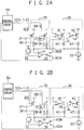
- the control circuit 50 controls the switches 34, 41, and 44 included in the correction circuit 30 as illustrated in FIG. 2A . That is, the control circuit 50 controls the switch 34 so as to connect the output of the operational amplifier and a signal line NDA in order to supply the output of the operational amplifier 31 to the control circuit 50. Further, the control circuit 50 controls the respective switches 41, 44 so that the power supply potential VDD is supplied to the gate of the PMOS transistor 39 and the reference potential VSS is supplied to the gate of the PMOS transistor 42.
- the power supply potential VDD is supplied to one of correction units in the fourth variable resistance unit 36 and the reference potential VSS is supplied to the other of the correction units, thereby making it possible to control the resistance values to increase or decrease at an analog correction time thereafter, or the like.
- control circuit 50 at an analog correction time after the digital code D[N-1:0] is determined and at a normal operation time, for example, controls the switches 34, 41, and 44 included in the correction circuit 30 as illustrated in FIG. 2B . That is, the control circuit 50 controls the switch 34 so as to connect the output of the operational amplifier 31 and the signal line NDB in order to output the output of the operational amplifier 31 as the analog control voltage. Further, the control circuit 50 controls the respective switches 41, 44 so that the analog control voltage is supplied to the gates of the PMOS transistors 39, 42. At this time, the control circuit 50 also controls the respective switches 17A, 17B, 20A, and 20B so that the analog control voltage is supplied to the gates of the PMOS transistors 15A, 15B, 18A, and 18B included in the amplifying circuit 10.
- the resistance values of the resistors 14A-i, 14B-i included in the first variable resistance unit of the amplifying circuit 10 and the resistance value of the resistor 38-i included in the third variable resistance unit 35 of the correction circuit 30 all may be the same or different.
- the resistance values being different, in processing to determine the digital code D[N - 1: 0], it is only necessary to set the resistance values so that as the order in which a value is determined becomes later, contribution to a combined resistance value by a resistance value corresponding to its bit becomes smaller.
- FIG. 3 is a flowchart illustrating an example of the resistance correction operation in this embodiment.
- the resistance correction operation is performed when the operation of the amplifier circuit starts, for example.
- step S301 initialization processing is performed at step S301, and the control circuit 50 cancels reset, and controls the respective switches to be brought into the state at a digital correction time illustrated in FIG. 2A . Further, the control circuit 50 resets all bits of the digital code D[N-1:0] to 0, and sets a count value i of a counter included therein to (N-1).
- step S302 the control circuit 50 sets an ith-bit digital code D[i] to "1" based on the count value i of the counter. Then, at step S303, the control circuit 50 judges whether or not the output of the operational amplifier 31 in the correction circuit 30 is positive.
- step S304 the control circuit 50 changes the ith-bit digital code D[i] to "0.”
- step S304 is skipped, and the control circuit 50 keeps the ith-bit digital code D[i] to "1.”
- the control circuit 50 judges whether or not the count value i of the counter is 0. In the case where the count value i of the counter is not 0, at step S306, the control circuit 50 subtracts 1 from the count value i of the counter and repeats the operations at and after step S302.
- the digital code D[i] is determined one bit by one bit sequentially and the count value i of the counter is judged to be 0 at step S305 as above, the digital code D[N-1:0] corresponding to a resistance value (first resistance value) according to the value of the reference voltage generated by the voltage supply 32 is determined. Then, at step S307, the control circuit 50 controls the respective switches to be brought into the state at an analog correction time illustrated in FIG. 2B .
- the output voltage of the operational amplifier 31 decreases.
- the voltage to be supplied to the gates of the PMOS transistors 39, 42 in the fourth variable resistance unit 36 decreases and the on-resistances of the PMOS transistors 39, 42 decrease.
- the on-resistances of the PMOS transistors 39, 42 decrease, and thereby voltage drop exhibiting to the current supplied by the current supply 33 decreases and the voltages generated by the third variable resistance unit 35 and the fourth variable resistance unit 36 increase.
- the analog control voltage is generated by the negative feedback of the operational amplifier 31 in this manner, thereby making it possible to control the analog control voltage so that the combined resistance value by the third variable resistance unit 35 and the fourth variable resistance unit 36 results in a desired resistance value.
- the digital code D[N-1:0] is determined, the analog control voltage is obtained, and the resistance correction operation is finished.
- the respective switches are controlled to be brought into the state illustrated in FIG. 2B even after the resistance correction operation is finished, and thus even with respect to the fluctuations in the resistance value caused by environmental changes such as temperature change, the analog control voltage is controlled, resulting in that it is possible to control the resistance values appropriately.
- the correction circuit 30 is used to control the digital code D[N-1:0] and the analog control voltage so that the resistance value of the resistance load in the amplifying circuit 10 becomes a desired resistance value, thereby making it possible to set the resistance value of the resistance load in the amplifying circuit 10 to a desired resistance value. Further, by the digital correction based on the digital code D[N-1:0], rough adjustment is performed, and by the analog correction based on the analog control voltage, fine adjustment is performed, thereby making it possible to accurately control the resistance value.
- an adjusted amount by the analog correction based on the analog control voltage in this embodiment is small as compared to that of a conventional method in which the resistance value is adjusted only by the analog correction, and thus it is possible to reduce the sensitivity of the analog control voltage with respect to the resistance value, resulting in an improvement in noise immunity.
- FIG. 4 is a diagram illustrating a configuration example of a semiconductor integrated circuit including the amplifier circuit in this embodiment.
- a semiconductor integrated circuit 401 in this embodiment includes a reception circuit 402 having a function of a deserializer circuit that converts an input serial signal to a parallel signal, and an internal circuit 409 such as a logic circuit that performs a processing operation by receiving a parallel signal (data) from the reception circuit 402.
- the reception circuit 402 includes a front end circuit 403, a clock data recovery circuit 407, and a clock generation circuit 408.
- the front end circuit 403 includes an amplifier circuit 404, a comparator (comparison circuit) 405, and a demultiplexer 406.
- the amplifier circuit 404 is the amplifier circuit in this embodiment and receives differential input serial signals RXIN, RXINX transmitted through a transmission path or the like. Use of the amplifier circuit in this embodiment makes it possible to correct variations or fluctuations in the resistance value of the resistance load to keep the resistance value to a constant value, and fabricate the front end circuit 403 in the reception circuit 402 with small variations in gain.
- the comparator 405 uses a clock signal output from the clock generation circuit 408 to sample the input serial signal at an appropriate timing and judges a data value (code) of the input serial signal.
- the demultiplexer 406 performs a serial-parallel conversion on an output of the comparator 405 to output the resultant as a parallel signal RXOUT.
- the clock data recovery circuit 407 appropriately controls the phase of a clock signal output from the clock generation circuit 408 based on a received signal.
- the internal circuit 409 receives the parallel signal RXOUT output from the reception circuit 402 to perform a processing operation relating to the parallel signal RXOUT, or the like.
- the amplifying circuit in this embodiment may have a circuit configuration called a CTLE (continuous time linear equalizer), which is designed to have frequency characteristics in which the gain of a high-frequency component is increased rather than the gain of a low-frequency component, on the assumption that an input signal made by the high-frequency component being attenuated by a transmission path is input.
- FIG. 5 illustrates a configuration example of the amplifier circuit in this embodiment having a circuit configuration called a CTLE.
- the same reference numerals and symbols are added to the same components as those illustrated in FIG. 1 , and their overlapping explanations are omitted.
- inductors 21A, 21B are provided between output terminals of the differential output signals OUTX, OUT and the variable resistance circuits included in the load circuit. Further, in order to consider parasitic resistance of the inductors, a similar inductor 45 is provided between the variable resistance circuits and the current supply in the correction circuit 30. Application of such a configuration makes it possible to obtain circuit characteristics such that an impedance is constant on the low-frequency side and increases on the high-frequency side by a series circuit of the inductor and the resistor. Further, application of this embodiment makes it possible to accurately control the resistance values of the variable resistance circuits to a constant value and obtain good frequency characteristics.
- the resistor to be disposed in parallel with the PMOS transistor is omitted, but the resistor may be disposed in parallel with the PMOS transistor.
- the switch 34 for supplying the output of the operational amplifier 31 included in the correction circuit 30 to one of the signal lines NDA and NDB is provided, even when the output of the operational amplifier 31 is designed to be supplied to the control circuit 50 as well as to be supplied as the analog control voltage without providing the switch 34, the similar operation is enabled.
- the two correction units are provided, but three or more correction units may be connected in parallel. Further, the potentials to be supplied to the gates of the PMOS transistors in the respective correction units at a digital correction time may be different.
Landscapes
- Engineering & Computer Science (AREA)
- Power Engineering (AREA)
- Physics & Mathematics (AREA)
- Nonlinear Science (AREA)
- Amplifiers (AREA)
- Semiconductor Integrated Circuits (AREA)
Applications Claiming Priority (1)
| Application Number | Priority Date | Filing Date | Title |
|---|---|---|---|
| PCT/JP2016/057748 WO2017154194A1 (ja) | 2016-03-11 | 2016-03-11 | 増幅回路、受信回路、及び半導体集積回路 |
Publications (3)
| Publication Number | Publication Date |
|---|---|
| EP3429079A1 true EP3429079A1 (de) | 2019-01-16 |
| EP3429079A4 EP3429079A4 (de) | 2019-03-27 |
| EP3429079B1 EP3429079B1 (de) | 2021-05-05 |
Family
ID=59790175
Family Applications (1)
| Application Number | Title | Priority Date | Filing Date |
|---|---|---|---|
| EP16893521.1A Active EP3429079B1 (de) | 2016-03-11 | 2016-03-11 | Verstärkerschaltung, empfänger und integrierte halbleiterschaltung |
Country Status (5)
| Country | Link |
|---|---|
| US (1) | US10742175B2 (de) |
| EP (1) | EP3429079B1 (de) |
| JP (1) | JP6725854B2 (de) |
| CN (1) | CN108781061B (de) |
| WO (1) | WO2017154194A1 (de) |
Families Citing this family (3)
| Publication number | Priority date | Publication date | Assignee | Title |
|---|---|---|---|---|
| CN112019171B (zh) * | 2019-05-31 | 2024-08-20 | 华邦电子股份有限公司 | 差动放大器 |
| KR20220057159A (ko) * | 2020-10-29 | 2022-05-09 | 에스케이하이닉스 주식회사 | 차동 입력 회로를 포함하는 반도체 장치 및 그의 캘리브레이션 방법 |
| US11881969B2 (en) * | 2022-04-22 | 2024-01-23 | Samsung Display Co., Ltd. | Real-time DC-balance aware AFE offset cancellation |
Family Cites Families (23)
| Publication number | Priority date | Publication date | Assignee | Title |
|---|---|---|---|---|
| JPH04135304A (ja) * | 1990-09-27 | 1992-05-08 | Nec Corp | 半導体集積回路 |
| JP4135304B2 (ja) * | 2000-09-25 | 2008-08-20 | コニカミノルタオプト株式会社 | 光学素子成形用金型の製造方法 |
| US6278325B1 (en) * | 2000-12-13 | 2001-08-21 | Industrial Technology Research Institute | Programmable gain amplifier with a large extent for the variation of gains |
| US6583660B2 (en) * | 2001-05-25 | 2003-06-24 | Infineon Technologies Ag | Active auto zero circuit for time continuous open loop amplifiers |
| US6621343B2 (en) | 2001-08-07 | 2003-09-16 | Infineon Technologies Ag | Open loop variable gain amplifier using replica gain cell |
| JP2003084728A (ja) | 2001-09-17 | 2003-03-19 | Citizen Watch Co Ltd | 液晶表示装置の電極駆動電圧発生回路 |
| US6958651B2 (en) * | 2002-12-03 | 2005-10-25 | Semiconductor Energy Laboratory Co., Ltd. | Analog circuit and display device using the same |
| US7034606B2 (en) * | 2004-05-07 | 2006-04-25 | Broadcom Corporation | VGA-CTF combination cell for 10 Gb/s serial data receivers |
| US20070103235A1 (en) * | 2005-11-04 | 2007-05-10 | Motorola, Inc. | Inductorless broadband RF low noise amplifier |
| US7403071B2 (en) * | 2006-03-14 | 2008-07-22 | Freescale Semiconductor, Inc. | High linearity and low noise amplifier with continuously variable gain control |
| JP2007248288A (ja) | 2006-03-16 | 2007-09-27 | Fujitsu Ltd | 温度特性補正方法及びセンサ用増幅回路 |
| JP2007303986A (ja) * | 2006-05-12 | 2007-11-22 | Advantest Corp | 直流試験装置 |
| US7417500B2 (en) * | 2006-06-19 | 2008-08-26 | Tzero Technologies, Inc. | Control of an adjustable gain amplifier |
| KR100952666B1 (ko) * | 2008-02-01 | 2010-04-13 | (주)에프씨아이 | 커패시터 피드백을 이용한 재구성 가능 저잡음 증폭기 |
| JP2009225205A (ja) * | 2008-03-18 | 2009-10-01 | Yokogawa Electric Corp | Cml回路 |
| JP2011055055A (ja) * | 2009-08-31 | 2011-03-17 | Texas Instr Japan Ltd | 増幅回路及び信号強度検出回路並びにオフセット電圧調整方法 |
| US8384465B2 (en) * | 2010-06-15 | 2013-02-26 | Aeroflex Colorado Springs Inc. | Amplitude-stabilized even order pre-distortion circuit |
| CN102195583B (zh) * | 2011-05-24 | 2016-01-20 | 中兴通讯股份有限公司 | 一种铌酸锂调制器跨阻放大器增益控制装置及方法 |
| JP5238856B2 (ja) * | 2011-06-23 | 2013-07-17 | ルネサスエレクトロニクス株式会社 | 差動増幅回路及びa/d変換器 |
| CN102969990A (zh) * | 2011-09-01 | 2013-03-13 | 联咏科技股份有限公司 | 具动态转导补偿的多输入差动放大器 |
| US8878608B2 (en) * | 2011-11-03 | 2014-11-04 | Mediatek Inc. | Comparator and amplifier |
| US9325287B2 (en) * | 2014-01-24 | 2016-04-26 | Applied Micro Circuits Corporation | Programmable gain amplifier with controlled gain steps |
| JP6399486B2 (ja) * | 2014-07-14 | 2018-10-03 | 株式会社エイアールテック | 演算増幅回路 |
-
2016
- 2016-03-11 CN CN201680083314.XA patent/CN108781061B/zh active Active
- 2016-03-11 EP EP16893521.1A patent/EP3429079B1/de active Active
- 2016-03-11 WO PCT/JP2016/057748 patent/WO2017154194A1/ja not_active Ceased
- 2016-03-11 JP JP2018503960A patent/JP6725854B2/ja active Active
-
2018
- 2018-08-23 US US16/110,801 patent/US10742175B2/en active Active
Also Published As
| Publication number | Publication date |
|---|---|
| US20180367103A1 (en) | 2018-12-20 |
| CN108781061A (zh) | 2018-11-09 |
| US10742175B2 (en) | 2020-08-11 |
| EP3429079B1 (de) | 2021-05-05 |
| WO2017154194A1 (ja) | 2017-09-14 |
| CN108781061B (zh) | 2022-04-08 |
| JP6725854B2 (ja) | 2020-07-22 |
| EP3429079A4 (de) | 2019-03-27 |
| JPWO2017154194A1 (ja) | 2019-01-17 |
Similar Documents
| Publication | Publication Date | Title |
|---|---|---|
| US7595676B2 (en) | Comparator and method with controllable threshold and hysteresis | |
| CN110915135B (zh) | 用于实施差分输入接收器的电路和方法 | |
| US7915913B2 (en) | Termination resistance adjusting circuit | |
| US9674008B2 (en) | Body-biased slicer design for predictive decision feedback equalizers | |
| US20130335135A1 (en) | Calibration circuit, integrated circuit having calibration circuit, and calibration method | |
| US9954503B2 (en) | Differential amplification circuit and semiconductor integrated circuit | |
| US9654315B2 (en) | Slicer apparatus and calibration method thereof | |
| US11899485B2 (en) | Line driver having adjustable current mirror array | |
| US10742175B2 (en) | Amplifier circuit, reception circuit, and semiconductor integrated circuit | |
| US20110133837A1 (en) | Variable gain amplifier | |
| KR20100041391A (ko) | 오프셋 조정회로 및 방법 | |
| US20130027092A1 (en) | Digital Output Driver | |
| US9331685B2 (en) | Comparator system | |
| US20040246760A1 (en) | Amplification circuit | |
| US9425776B2 (en) | Method for detecting hysteresis characteristic of comparator and semiconductor device | |
| US20120223736A1 (en) | Transceiving circuit and transceiving circuit resistance calibration method | |
| US12113494B2 (en) | Differential amplifier circuit, reception circuit, and semiconductor integrated circuit | |
| EP2779445A1 (de) | Dreistufiger Verstärker | |
| US7474133B1 (en) | Apparatus and method for high-speed serial communications | |
| US7477077B1 (en) | Apparatus and method for loss of signal detection in a receiver | |
| US7816971B2 (en) | Switch circuit having adjustable linearity of differential mode resistances | |
| US9134360B2 (en) | Method and apparatus for feedback-based resistance calibration | |
| JP5369472B2 (ja) | 半導体装置 |
Legal Events
| Date | Code | Title | Description |
|---|---|---|---|
| STAA | Information on the status of an ep patent application or granted ep patent |
Free format text: STATUS: THE INTERNATIONAL PUBLICATION HAS BEEN MADE |
|
| PUAI | Public reference made under article 153(3) epc to a published international application that has entered the european phase |
Free format text: ORIGINAL CODE: 0009012 |
|
| STAA | Information on the status of an ep patent application or granted ep patent |
Free format text: STATUS: REQUEST FOR EXAMINATION WAS MADE |
|
| 17P | Request for examination filed |
Effective date: 20180824 |
|
| AK | Designated contracting states |
Kind code of ref document: A1 Designated state(s): AL AT BE BG CH CY CZ DE DK EE ES FI FR GB GR HR HU IE IS IT LI LT LU LV MC MK MT NL NO PL PT RO RS SE SI SK SM TR |
|
| AX | Request for extension of the european patent |
Extension state: BA ME |
|
| A4 | Supplementary search report drawn up and despatched |
Effective date: 20190222 |
|
| RIC1 | Information provided on ipc code assigned before grant |
Ipc: H03F 3/45 20060101AFI20190218BHEP Ipc: H03G 1/00 20060101ALI20190218BHEP Ipc: H03G 3/30 20060101ALI20190218BHEP |
|
| DAV | Request for validation of the european patent (deleted) | ||
| DAX | Request for extension of the european patent (deleted) | ||
| STAA | Information on the status of an ep patent application or granted ep patent |
Free format text: STATUS: EXAMINATION IS IN PROGRESS |
|
| 17Q | First examination report despatched |
Effective date: 20200325 |
|
| REG | Reference to a national code |
Ref country code: DE Ref legal event code: R079 Ref document number: 602016057614 Country of ref document: DE Free format text: PREVIOUS MAIN CLASS: H03F0003450000 Ipc: H03F0001300000 |
|
| GRAP | Despatch of communication of intention to grant a patent |
Free format text: ORIGINAL CODE: EPIDOSNIGR1 |
|
| STAA | Information on the status of an ep patent application or granted ep patent |
Free format text: STATUS: GRANT OF PATENT IS INTENDED |
|
| RIC1 | Information provided on ipc code assigned before grant |
Ipc: H03G 3/00 20060101ALI20200925BHEP Ipc: H03G 3/30 20060101ALI20200925BHEP Ipc: H03F 3/45 20060101ALI20200925BHEP Ipc: H03F 1/30 20060101AFI20200925BHEP Ipc: H03G 1/00 20060101ALI20200925BHEP |
|
| INTG | Intention to grant announced |
Effective date: 20201016 |
|
| GRAS | Grant fee paid |
Free format text: ORIGINAL CODE: EPIDOSNIGR3 |
|
| GRAA | (expected) grant |
Free format text: ORIGINAL CODE: 0009210 |
|
| STAA | Information on the status of an ep patent application or granted ep patent |
Free format text: STATUS: THE PATENT HAS BEEN GRANTED |
|
| AK | Designated contracting states |
Kind code of ref document: B1 Designated state(s): AL AT BE BG CH CY CZ DE DK EE ES FI FR GB GR HR HU IE IS IT LI LT LU LV MC MK MT NL NO PL PT RO RS SE SI SK SM TR |
|
| REG | Reference to a national code |
Ref country code: GB Ref legal event code: FG4D |
|
| REG | Reference to a national code |
Ref country code: CH Ref legal event code: EP |
|
| REG | Reference to a national code |
Ref country code: AT Ref legal event code: REF Ref document number: 1391100 Country of ref document: AT Kind code of ref document: T Effective date: 20210515 |
|
| REG | Reference to a national code |
Ref country code: IE Ref legal event code: FG4D |
|
| REG | Reference to a national code |
Ref country code: DE Ref legal event code: R096 Ref document number: 602016057614 Country of ref document: DE |
|
| REG | Reference to a national code |
Ref country code: LT Ref legal event code: MG9D |
|
| REG | Reference to a national code |
Ref country code: AT Ref legal event code: MK05 Ref document number: 1391100 Country of ref document: AT Kind code of ref document: T Effective date: 20210505 |
|
| PG25 | Lapsed in a contracting state [announced via postgrant information from national office to epo] |
Ref country code: FI Free format text: LAPSE BECAUSE OF FAILURE TO SUBMIT A TRANSLATION OF THE DESCRIPTION OR TO PAY THE FEE WITHIN THE PRESCRIBED TIME-LIMIT Effective date: 20210505 Ref country code: LT Free format text: LAPSE BECAUSE OF FAILURE TO SUBMIT A TRANSLATION OF THE DESCRIPTION OR TO PAY THE FEE WITHIN THE PRESCRIBED TIME-LIMIT Effective date: 20210505 Ref country code: HR Free format text: LAPSE BECAUSE OF FAILURE TO SUBMIT A TRANSLATION OF THE DESCRIPTION OR TO PAY THE FEE WITHIN THE PRESCRIBED TIME-LIMIT Effective date: 20210505 Ref country code: AT Free format text: LAPSE BECAUSE OF FAILURE TO SUBMIT A TRANSLATION OF THE DESCRIPTION OR TO PAY THE FEE WITHIN THE PRESCRIBED TIME-LIMIT Effective date: 20210505 Ref country code: BG Free format text: LAPSE BECAUSE OF FAILURE TO SUBMIT A TRANSLATION OF THE DESCRIPTION OR TO PAY THE FEE WITHIN THE PRESCRIBED TIME-LIMIT Effective date: 20210805 |
|
| PG25 | Lapsed in a contracting state [announced via postgrant information from national office to epo] |
Ref country code: GR Free format text: LAPSE BECAUSE OF FAILURE TO SUBMIT A TRANSLATION OF THE DESCRIPTION OR TO PAY THE FEE WITHIN THE PRESCRIBED TIME-LIMIT Effective date: 20210806 Ref country code: LV Free format text: LAPSE BECAUSE OF FAILURE TO SUBMIT A TRANSLATION OF THE DESCRIPTION OR TO PAY THE FEE WITHIN THE PRESCRIBED TIME-LIMIT Effective date: 20210505 Ref country code: IS Free format text: LAPSE BECAUSE OF FAILURE TO SUBMIT A TRANSLATION OF THE DESCRIPTION OR TO PAY THE FEE WITHIN THE PRESCRIBED TIME-LIMIT Effective date: 20210905 Ref country code: SE Free format text: LAPSE BECAUSE OF FAILURE TO SUBMIT A TRANSLATION OF THE DESCRIPTION OR TO PAY THE FEE WITHIN THE PRESCRIBED TIME-LIMIT Effective date: 20210505 Ref country code: RS Free format text: LAPSE BECAUSE OF FAILURE TO SUBMIT A TRANSLATION OF THE DESCRIPTION OR TO PAY THE FEE WITHIN THE PRESCRIBED TIME-LIMIT Effective date: 20210505 Ref country code: NO Free format text: LAPSE BECAUSE OF FAILURE TO SUBMIT A TRANSLATION OF THE DESCRIPTION OR TO PAY THE FEE WITHIN THE PRESCRIBED TIME-LIMIT Effective date: 20210805 Ref country code: PT Free format text: LAPSE BECAUSE OF FAILURE TO SUBMIT A TRANSLATION OF THE DESCRIPTION OR TO PAY THE FEE WITHIN THE PRESCRIBED TIME-LIMIT Effective date: 20210906 Ref country code: PL Free format text: LAPSE BECAUSE OF FAILURE TO SUBMIT A TRANSLATION OF THE DESCRIPTION OR TO PAY THE FEE WITHIN THE PRESCRIBED TIME-LIMIT Effective date: 20210505 |
|
| REG | Reference to a national code |
Ref country code: NL Ref legal event code: MP Effective date: 20210505 |
|
| PG25 | Lapsed in a contracting state [announced via postgrant information from national office to epo] |
Ref country code: NL Free format text: LAPSE BECAUSE OF FAILURE TO SUBMIT A TRANSLATION OF THE DESCRIPTION OR TO PAY THE FEE WITHIN THE PRESCRIBED TIME-LIMIT Effective date: 20210505 |
|
| PG25 | Lapsed in a contracting state [announced via postgrant information from national office to epo] |
Ref country code: SK Free format text: LAPSE BECAUSE OF FAILURE TO SUBMIT A TRANSLATION OF THE DESCRIPTION OR TO PAY THE FEE WITHIN THE PRESCRIBED TIME-LIMIT Effective date: 20210505 Ref country code: SM Free format text: LAPSE BECAUSE OF FAILURE TO SUBMIT A TRANSLATION OF THE DESCRIPTION OR TO PAY THE FEE WITHIN THE PRESCRIBED TIME-LIMIT Effective date: 20210505 Ref country code: EE Free format text: LAPSE BECAUSE OF FAILURE TO SUBMIT A TRANSLATION OF THE DESCRIPTION OR TO PAY THE FEE WITHIN THE PRESCRIBED TIME-LIMIT Effective date: 20210505 Ref country code: DK Free format text: LAPSE BECAUSE OF FAILURE TO SUBMIT A TRANSLATION OF THE DESCRIPTION OR TO PAY THE FEE WITHIN THE PRESCRIBED TIME-LIMIT Effective date: 20210505 Ref country code: CZ Free format text: LAPSE BECAUSE OF FAILURE TO SUBMIT A TRANSLATION OF THE DESCRIPTION OR TO PAY THE FEE WITHIN THE PRESCRIBED TIME-LIMIT Effective date: 20210505 Ref country code: RO Free format text: LAPSE BECAUSE OF FAILURE TO SUBMIT A TRANSLATION OF THE DESCRIPTION OR TO PAY THE FEE WITHIN THE PRESCRIBED TIME-LIMIT Effective date: 20210505 Ref country code: ES Free format text: LAPSE BECAUSE OF FAILURE TO SUBMIT A TRANSLATION OF THE DESCRIPTION OR TO PAY THE FEE WITHIN THE PRESCRIBED TIME-LIMIT Effective date: 20210505 |
|
| REG | Reference to a national code |
Ref country code: DE Ref legal event code: R097 Ref document number: 602016057614 Country of ref document: DE |
|
| PLBE | No opposition filed within time limit |
Free format text: ORIGINAL CODE: 0009261 |
|
| STAA | Information on the status of an ep patent application or granted ep patent |
Free format text: STATUS: NO OPPOSITION FILED WITHIN TIME LIMIT |
|
| 26N | No opposition filed |
Effective date: 20220208 |
|
| PG25 | Lapsed in a contracting state [announced via postgrant information from national office to epo] |
Ref country code: IS Free format text: LAPSE BECAUSE OF FAILURE TO SUBMIT A TRANSLATION OF THE DESCRIPTION OR TO PAY THE FEE WITHIN THE PRESCRIBED TIME-LIMIT Effective date: 20210905 Ref country code: AL Free format text: LAPSE BECAUSE OF FAILURE TO SUBMIT A TRANSLATION OF THE DESCRIPTION OR TO PAY THE FEE WITHIN THE PRESCRIBED TIME-LIMIT Effective date: 20210505 |
|
| PG25 | Lapsed in a contracting state [announced via postgrant information from national office to epo] |
Ref country code: IT Free format text: LAPSE BECAUSE OF FAILURE TO SUBMIT A TRANSLATION OF THE DESCRIPTION OR TO PAY THE FEE WITHIN THE PRESCRIBED TIME-LIMIT Effective date: 20210505 |
|
| PG25 | Lapsed in a contracting state [announced via postgrant information from national office to epo] |
Ref country code: MC Free format text: LAPSE BECAUSE OF FAILURE TO SUBMIT A TRANSLATION OF THE DESCRIPTION OR TO PAY THE FEE WITHIN THE PRESCRIBED TIME-LIMIT Effective date: 20210505 |
|
| REG | Reference to a national code |
Ref country code: CH Ref legal event code: PL |
|
| GBPC | Gb: european patent ceased through non-payment of renewal fee |
Effective date: 20220311 |
|
| REG | Reference to a national code |
Ref country code: BE Ref legal event code: MM Effective date: 20220331 |
|
| PG25 | Lapsed in a contracting state [announced via postgrant information from national office to epo] |
Ref country code: LU Free format text: LAPSE BECAUSE OF NON-PAYMENT OF DUE FEES Effective date: 20220311 Ref country code: LI Free format text: LAPSE BECAUSE OF NON-PAYMENT OF DUE FEES Effective date: 20220331 Ref country code: IE Free format text: LAPSE BECAUSE OF NON-PAYMENT OF DUE FEES Effective date: 20220311 Ref country code: GB Free format text: LAPSE BECAUSE OF NON-PAYMENT OF DUE FEES Effective date: 20220311 Ref country code: FR Free format text: LAPSE BECAUSE OF NON-PAYMENT OF DUE FEES Effective date: 20220331 Ref country code: CH Free format text: LAPSE BECAUSE OF NON-PAYMENT OF DUE FEES Effective date: 20220331 |
|
| PG25 | Lapsed in a contracting state [announced via postgrant information from national office to epo] |
Ref country code: BE Free format text: LAPSE BECAUSE OF NON-PAYMENT OF DUE FEES Effective date: 20220331 |
|
| PG25 | Lapsed in a contracting state [announced via postgrant information from national office to epo] |
Ref country code: HU Free format text: LAPSE BECAUSE OF FAILURE TO SUBMIT A TRANSLATION OF THE DESCRIPTION OR TO PAY THE FEE WITHIN THE PRESCRIBED TIME-LIMIT; INVALID AB INITIO Effective date: 20160311 |
|
| PG25 | Lapsed in a contracting state [announced via postgrant information from national office to epo] |
Ref country code: MK Free format text: LAPSE BECAUSE OF FAILURE TO SUBMIT A TRANSLATION OF THE DESCRIPTION OR TO PAY THE FEE WITHIN THE PRESCRIBED TIME-LIMIT Effective date: 20210505 Ref country code: CY Free format text: LAPSE BECAUSE OF FAILURE TO SUBMIT A TRANSLATION OF THE DESCRIPTION OR TO PAY THE FEE WITHIN THE PRESCRIBED TIME-LIMIT Effective date: 20210505 |
|
| PG25 | Lapsed in a contracting state [announced via postgrant information from national office to epo] |
Ref country code: TR Free format text: LAPSE BECAUSE OF FAILURE TO SUBMIT A TRANSLATION OF THE DESCRIPTION OR TO PAY THE FEE WITHIN THE PRESCRIBED TIME-LIMIT Effective date: 20210505 |
|
| PG25 | Lapsed in a contracting state [announced via postgrant information from national office to epo] |
Ref country code: MT Free format text: LAPSE BECAUSE OF FAILURE TO SUBMIT A TRANSLATION OF THE DESCRIPTION OR TO PAY THE FEE WITHIN THE PRESCRIBED TIME-LIMIT Effective date: 20210505 |
|
| PGFP | Annual fee paid to national office [announced via postgrant information from national office to epo] |
Ref country code: DE Payment date: 20260319 Year of fee payment: 11 |