EP3422405B1 - Fingerprint sensor chip package - Google Patents
Fingerprint sensor chip package Download PDFInfo
- Publication number
- EP3422405B1 EP3422405B1 EP17892751.3A EP17892751A EP3422405B1 EP 3422405 B1 EP3422405 B1 EP 3422405B1 EP 17892751 A EP17892751 A EP 17892751A EP 3422405 B1 EP3422405 B1 EP 3422405B1
- Authority
- EP
- European Patent Office
- Prior art keywords
- connecting rib
- chip
- base island
- rib
- finger
- Prior art date
- Legal status (The legal status is an assumption and is not a legal conclusion. Google has not performed a legal analysis and makes no representation as to the accuracy of the status listed.)
- Active
Links
Images


Classifications
-
- H—ELECTRICITY
- H10—SEMICONDUCTOR DEVICES; ELECTRIC SOLID-STATE DEVICES NOT OTHERWISE PROVIDED FOR
- H10W—GENERIC PACKAGES, INTERCONNECTIONS, CONNECTORS OR OTHER CONSTRUCTIONAL DETAILS OF DEVICES COVERED BY CLASS H10
- H10W70/00—Package substrates; Interposers; Redistribution layers [RDL]
- H10W70/40—Leadframes
- H10W70/411—Chip-supporting parts, e.g. die pads
- H10W70/415—Leadframe inner leads serving as die pads
-
- G—PHYSICS
- G06—COMPUTING OR CALCULATING; COUNTING
- G06V—IMAGE OR VIDEO RECOGNITION OR UNDERSTANDING
- G06V40/00—Recognition of biometric, human-related or animal-related patterns in image or video data
- G06V40/10—Human or animal bodies, e.g. vehicle occupants or pedestrians; Body parts, e.g. hands
- G06V40/12—Fingerprints or palmprints
-
- G—PHYSICS
- G06—COMPUTING OR CALCULATING; COUNTING
- G06V—IMAGE OR VIDEO RECOGNITION OR UNDERSTANDING
- G06V40/00—Recognition of biometric, human-related or animal-related patterns in image or video data
- G06V40/10—Human or animal bodies, e.g. vehicle occupants or pedestrians; Body parts, e.g. hands
- G06V40/12—Fingerprints or palmprints
- G06V40/13—Sensors therefor
-
- H—ELECTRICITY
- H10—SEMICONDUCTOR DEVICES; ELECTRIC SOLID-STATE DEVICES NOT OTHERWISE PROVIDED FOR
- H10P—GENERIC PROCESSES OR APPARATUS FOR THE MANUFACTURE OR TREATMENT OF DEVICES COVERED BY CLASS H10
- H10P74/00—Testing or measuring during manufacture or treatment of wafers, substrates or devices
- H10P74/20—Testing or measuring during manufacture or treatment of wafers, substrates or devices characterised by the properties tested or measured, e.g. structural or electrical properties
- H10P74/207—Electrical properties, e.g. testing or measuring of resistance, deep levels or capacitance-voltage characteristics
-
- H—ELECTRICITY
- H10—SEMICONDUCTOR DEVICES; ELECTRIC SOLID-STATE DEVICES NOT OTHERWISE PROVIDED FOR
- H10P—GENERIC PROCESSES OR APPARATUS FOR THE MANUFACTURE OR TREATMENT OF DEVICES COVERED BY CLASS H10
- H10P74/00—Testing or measuring during manufacture or treatment of wafers, substrates or devices
- H10P74/27—Structural arrangements therefor
- H10P74/273—Interconnections for measuring or testing, e.g. probe pads
-
- H—ELECTRICITY
- H10—SEMICONDUCTOR DEVICES; ELECTRIC SOLID-STATE DEVICES NOT OTHERWISE PROVIDED FOR
- H10W—GENERIC PACKAGES, INTERCONNECTIONS, CONNECTORS OR OTHER CONSTRUCTIONAL DETAILS OF DEVICES COVERED BY CLASS H10
- H10W70/00—Package substrates; Interposers; Redistribution layers [RDL]
- H10W70/01—Manufacture or treatment
- H10W70/04—Manufacture or treatment of leadframes
- H10W70/041—Connecting or disconnecting interconnections to or from leadframes, e.g. connecting bond wires or bumps
-
- H—ELECTRICITY
- H10—SEMICONDUCTOR DEVICES; ELECTRIC SOLID-STATE DEVICES NOT OTHERWISE PROVIDED FOR
- H10W—GENERIC PACKAGES, INTERCONNECTIONS, CONNECTORS OR OTHER CONSTRUCTIONAL DETAILS OF DEVICES COVERED BY CLASS H10
- H10W70/00—Package substrates; Interposers; Redistribution layers [RDL]
- H10W70/01—Manufacture or treatment
- H10W70/04—Manufacture or treatment of leadframes
- H10W70/042—Etching
-
- H—ELECTRICITY
- H10—SEMICONDUCTOR DEVICES; ELECTRIC SOLID-STATE DEVICES NOT OTHERWISE PROVIDED FOR
- H10W—GENERIC PACKAGES, INTERCONNECTIONS, CONNECTORS OR OTHER CONSTRUCTIONAL DETAILS OF DEVICES COVERED BY CLASS H10
- H10W70/00—Package substrates; Interposers; Redistribution layers [RDL]
- H10W70/40—Leadframes
- H10W70/421—Shapes or dispositions
-
- H—ELECTRICITY
- H10—SEMICONDUCTOR DEVICES; ELECTRIC SOLID-STATE DEVICES NOT OTHERWISE PROVIDED FOR
- H10W—GENERIC PACKAGES, INTERCONNECTIONS, CONNECTORS OR OTHER CONSTRUCTIONAL DETAILS OF DEVICES COVERED BY CLASS H10
- H10W72/00—Interconnections or connectors in packages
- H10W72/071—Connecting or disconnecting
- H10W72/073—Connecting or disconnecting of die-attach connectors
-
- H—ELECTRICITY
- H10—SEMICONDUCTOR DEVICES; ELECTRIC SOLID-STATE DEVICES NOT OTHERWISE PROVIDED FOR
- H10W—GENERIC PACKAGES, INTERCONNECTIONS, CONNECTORS OR OTHER CONSTRUCTIONAL DETAILS OF DEVICES COVERED BY CLASS H10
- H10W74/00—Encapsulations, e.g. protective coatings
- H10W74/01—Manufacture or treatment
-
- H—ELECTRICITY
- H10—SEMICONDUCTOR DEVICES; ELECTRIC SOLID-STATE DEVICES NOT OTHERWISE PROVIDED FOR
- H10W—GENERIC PACKAGES, INTERCONNECTIONS, CONNECTORS OR OTHER CONSTRUCTIONAL DETAILS OF DEVICES COVERED BY CLASS H10
- H10W74/00—Encapsulations, e.g. protective coatings
- H10W74/01—Manufacture or treatment
- H10W74/016—Manufacture or treatment using moulds
-
- H—ELECTRICITY
- H10—SEMICONDUCTOR DEVICES; ELECTRIC SOLID-STATE DEVICES NOT OTHERWISE PROVIDED FOR
- H10W—GENERIC PACKAGES, INTERCONNECTIONS, CONNECTORS OR OTHER CONSTRUCTIONAL DETAILS OF DEVICES COVERED BY CLASS H10
- H10W74/00—Encapsulations, e.g. protective coatings
- H10W74/10—Encapsulations, e.g. protective coatings characterised by their shape or disposition
- H10W74/111—Encapsulations, e.g. protective coatings characterised by their shape or disposition the semiconductor body being completely enclosed
- H10W74/114—Encapsulations, e.g. protective coatings characterised by their shape or disposition the semiconductor body being completely enclosed by a substrate and the encapsulations
-
- H—ELECTRICITY
- H10—SEMICONDUCTOR DEVICES; ELECTRIC SOLID-STATE DEVICES NOT OTHERWISE PROVIDED FOR
- H10W—GENERIC PACKAGES, INTERCONNECTIONS, CONNECTORS OR OTHER CONSTRUCTIONAL DETAILS OF DEVICES COVERED BY CLASS H10
- H10W70/00—Package substrates; Interposers; Redistribution layers [RDL]
- H10W70/40—Leadframes
- H10W70/456—Materials
- H10W70/457—Materials of metallic layers on leadframes
-
- H—ELECTRICITY
- H10—SEMICONDUCTOR DEVICES; ELECTRIC SOLID-STATE DEVICES NOT OTHERWISE PROVIDED FOR
- H10W—GENERIC PACKAGES, INTERCONNECTIONS, CONNECTORS OR OTHER CONSTRUCTIONAL DETAILS OF DEVICES COVERED BY CLASS H10
- H10W72/00—Interconnections or connectors in packages
- H10W72/071—Connecting or disconnecting
- H10W72/075—Connecting or disconnecting of bond wires
-
- H—ELECTRICITY
- H10—SEMICONDUCTOR DEVICES; ELECTRIC SOLID-STATE DEVICES NOT OTHERWISE PROVIDED FOR
- H10W—GENERIC PACKAGES, INTERCONNECTIONS, CONNECTORS OR OTHER CONSTRUCTIONAL DETAILS OF DEVICES COVERED BY CLASS H10
- H10W72/00—Interconnections or connectors in packages
- H10W72/50—Bond wires
- H10W72/59—Bond pads specially adapted therefor
-
- H—ELECTRICITY
- H10—SEMICONDUCTOR DEVICES; ELECTRIC SOLID-STATE DEVICES NOT OTHERWISE PROVIDED FOR
- H10W—GENERIC PACKAGES, INTERCONNECTIONS, CONNECTORS OR OTHER CONSTRUCTIONAL DETAILS OF DEVICES COVERED BY CLASS H10
- H10W72/00—Interconnections or connectors in packages
- H10W72/90—Bond pads, in general
- H10W72/951—Materials of bond pads
- H10W72/952—Materials of bond pads comprising metals or metalloids, e.g. PbSn, Ag or Cu
-
- H—ELECTRICITY
- H10—SEMICONDUCTOR DEVICES; ELECTRIC SOLID-STATE DEVICES NOT OTHERWISE PROVIDED FOR
- H10W—GENERIC PACKAGES, INTERCONNECTIONS, CONNECTORS OR OTHER CONSTRUCTIONAL DETAILS OF DEVICES COVERED BY CLASS H10
- H10W74/00—Encapsulations, e.g. protective coatings
- H10W74/10—Encapsulations, e.g. protective coatings characterised by their shape or disposition
- H10W74/111—Encapsulations, e.g. protective coatings characterised by their shape or disposition the semiconductor body being completely enclosed
-
- H—ELECTRICITY
- H10—SEMICONDUCTOR DEVICES; ELECTRIC SOLID-STATE DEVICES NOT OTHERWISE PROVIDED FOR
- H10W—GENERIC PACKAGES, INTERCONNECTIONS, CONNECTORS OR OTHER CONSTRUCTIONAL DETAILS OF DEVICES COVERED BY CLASS H10
- H10W90/00—Package configurations
- H10W90/701—Package configurations characterised by the relative positions of pads or connectors relative to package parts
- H10W90/751—Package configurations characterised by the relative positions of pads or connectors relative to package parts of bond wires
- H10W90/756—Package configurations characterised by the relative positions of pads or connectors relative to package parts of bond wires between a chip and a stacked lead frame, conducting package substrate or heat sink
Definitions
- the present invention relates to the field of biometric identification, in particular, to a fingerprint-sensor chip package and method for processing same.
- a fingerprint chip package needs to be cut into different shapes according to different requirements of customers. Therefore, it is generally shipped in strips, it will be tested first before being shipped, which is also called test in strips.
- FIG. 1 is an internal structural diagram of a package body with existing common lead frame type, a connecting rib connects with all the components of the lead frame, including a base island for placing chips and golden fingers for connecting the package with an external PCB (printed circuit board), to achieve a physical connection; in the process of packaging, an electrical connection is achieved by a connection between the internal components of the lead frame and the aluminum pad of the chip through a bonding wire. Different components will be given different electrical signals. Since all the components are connected by the connecting rib, all the components are electrically short-circuited and the test in strips cannot be performed.
- PCB printed circuit board
- the connecting ribs supporting the base island within one unit of the lead frame.
- the connecting ribs are deformed easily since it is too long, which causes the base island to lean.
- the fingerprint chip generally has a large area.
- an abnormality in a deformation of the lead frame occurs easily, which effects the production stability and the yield.
- connecting ribs are made of metal and are less likely to be cut than the package with plastic element.
- each device area in a lead frame panel has a die attach pad and a multiplicity of conductive contacts.
- the contacts are carried by tie bars and the die attach pad is carried by support bars that extend from the contacts.
- the lead frame panel is held in position while the die attach pad support bars are severed.
- an adhesive tape is adhered to the bottom surface of the lead frame panel so that the die attach pad may be held in position relative to its associated contacts. After the adhesive tape has been applied, the leadless packages may be assembled in a conventional manner.
- FIG. 8 further shows the package 100 after bonding a wire 830 (e.g., gold wire) from a landing pad 840 of the electronic device 810 to the portion of lead 110 covered with the metal plate 610.
- the wire 830 facilitates the electrical interconnection of the electronic device 810 to other devices (not shown) of, or external to, the package 100.
- a plurality of wire bonds are formed between the landing pads 840 and leads 110, but for clarity, only a few connections are depicted.
- JP S55-21124 A discloses a metallic lead frame has a tap lead 13 for carry in its internal end a tab 12 for attaching a semiconductor element and a frame member for carrying the tab lead 13 and the outer end of a lead 14.
- the outer end of the tab lead 13 and lead 14 are extended from the frame member 10 and supported by the frame member 10 through a bent buffer piece 19 transformable easily along the face direction of the lead frame.
- the present invention provides a fingerprint chip package and method for processing same, which solves the problem of the instability of the current fingerprint chip packaging structure.
- the present invention provides a fingerprint-sensor chip package, including: a lead frame, a chip, and a plastic packaging part enclosing the lead frame and the chip; where the lead frame includes a base island, a connecting rib, the connecting rib being a mental frame with four sides, and at least one connecting finger provided on each side of the connecting rib, and the base island is in the middle region of the lead frame surrounded by the connecting rib; the chip is adhered to the base island; the base island is fixedly connected to the connecting rib via the connecting fingers on at least two sides of the connecting rib; the chip is electrically connected to the at least one connecting finger on at least one side of the connecting rib that is not fixedly connected to the base island by connecting fingers by a bonding wire; the connecting rib is disconnected from the at least one connecting finger that is connected to the chip by the bonding wire.
- the at least one connecting fingers on three sides of the connecting rib are fixedly connected with the base island, and the at least one connecting finger on one side is disconnected from the connecting rib and electrically connected with the chip.
- a plurality of aluminum pads are provided on the chip; and the aluminum pads on the chip are connected with respective ones of the connecting fingers in a one-to-one correspondence using the bonding wires.
- the present invention provides a method for processing a fingerprint-sensor chip package, used for processing the above fingerprint-sensor chip package, including: adhering a chip to a base island of a lead frame, wherein the lead frame comprises a base island, a connecting rib, the connecting rib being a mental frame with four sides, and at least one connecting finger provided on each side of the connecting rib, and the base island is in the middle region of the lead frame surrounded by the connecting rib; wherein the base island is fixedly connected to the connecting rib via the connecting fingers on at least two sides of the connecting rib; electrically connecting with the chip and the at least one connecting finger on at least one side of a connecting rib that is not fixedly connected to the base island by connecting fingers using a bonding wire; injection molding the fingerprint-sensor chip
- the disconnecting of the electrical connection between the connecting rib and the at least one connecting finger electrically connected with the chip includes: back-etching connecting rib to disconnect the electrical connection between the connecting rib and the at least one connecting finger that is electrically connected with the chip.
- the present invention has the following advantages: The cutting difficulty of the fingerprint chip package is effectively reduced, and the efficiency of separation of single package is improved. And the contact area between the connecting fingers on the multiple sides of the connecting rib and the base island is larger than the contact area between the connecting rib and the base island in the prior art, and thus the production stability of the adhesion of chip and connection of bonding wire is improved. And the connecting rib on the end of the connecting fingers electrically connected with the chip is etched completely, so that the electrical connections between each internal components of the fingerprint chip package and the adjacent fingerprint chip package are all disconnected. The test in strips to the fingerprint chip package can be achieved.
- a process, method, system, product, or device that comprises a series of steps or units is not limited to the listed steps or units, but may also optionally includes steps or units that are not listed, or may also optionally includes other steps or units that inherent to the process, method, product, or device.
- an embodiment means that a particular feature, structure, or characteristic described in combination with an embodiment can be included in at least one embodiment of the present invention.
- the phrases appeared in various places of the description do not necessarily all refer to the same embodiment, nor are they independent or alternative embodiments that are mutually exclusive from other embodiments. It will be understood by those skilled in the art, both explicitly and implicitly, that the embodiments described herein can be combined with other embodiments.
- the fingerprint chip package includes a lead frame 1, a chip 2, and a plastic packaging part (not shown) enclosing the lead frame 1 and the chip 2.
- the chip 2 is disposed in the middle region of the lead frame 1 and is fixedly connected with the lead frame 1, and the chip 2 is a silicon-based fingerprint chip. In other implementations, the chip 2 may also be a chip of other materials or other functions.
- the lead frame 1 is a carrier of the chip 2 and is mainly used for connecting with an internal circuit of the chip 2 and an external PCB.
- the chip 2 is adhered and fixed to the lead frame 1, and the lead frame 1 includes a base island 13, a connecting rib 11 and a connecting finger 12.
- the connecting rib 11 is a frame made of metal material and includes four sides, which are structures that are physically connected with all the components in the lead frame. At least one connecting finger 12 is provided on each side of the connecting rib 11.
- the connecting rib 11 is used for supporting the lead frame 1 and connecting with the base island 13 via the connecting finger 12.
- the connecting finger 12 is used for electrically connecting the chip 2 with the external structure of the fingerprint chip package as well as fixing the base island 13.
- the number of the connecting finger 12 on each side of the connecting rib 11 is set according to actual requirements. In the embodiment of the present invention, the number of the connecting finger 12 on each side of the connecting rib 11 is the same. In other implementations of the present invention, the number of the connecting finger 12 on each side of the connecting rib 11 may also be different.
- a base island 13 is provided in the middle region of the lead frame 1.
- the base island 13 is fixedly connected with the connecting finger 12 on at least two sides.
- the chip 2 is fixedly provided on the base island 13.
- At least one aluminum pad 21 is provided on the chip 2, the aluminum pad 21 is electrically connected with the connecting finger 12 on at least one side via a bonding wire 3.
- the connecting finger 12 on the remaining side is fixedly connected with the base island 13.
- the chip 2 transmits the electric signal to the structure of external PCB via the electrical connection with the connecting finger 12.
- the number and arrangement of connecting fingers connected with the aluminum pad 21 via the bonding wire 3 may be flexibly selected, which may be continuously arranged or dispersedly arranged, and the number is not limited to one row.
- the connecting rib 11 is not processed in the embodiment of the present invention at first. After the injection molding of the plastic packaging part is completed, since the back surface of the connecting rib 11 is located on the same plane with the injection-molded template, the back surface of the connecting rib 11 is not covered by the injection-molded material. After the injection molding of a plastic packaging part is completed, the connecting rib 11 may be etched, so that the electrical connection between the connecting fingers 12 and the adjacent single package is disconnected. Specifically:
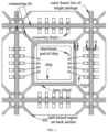
- the light-colored region in the figure is a position where the connecting rib 11 is half-etched and the dark-colored region in the figure is a position where the connecting rib 11 is completely etched.
- the base island 13 is fixedly connected with the connecting finger 12 on any three sides of the connecting rib 11.
- the aluminum pad 21 is electrically connected with the connecting finger 12 on the fourth side of the connecting rib 11 via the bonding wire 3.
- the size and distribution of the region of the connecting rib 11 connected with the base island 13 and the size and distribution of the region of the connecting rib 11 at the end of the connecting finger 12 electrically connected with the chip 2 may be flexibly selected. Before the plastic packaging part is injection molded, the connecting rib 11 is not etched.
- the three sides of the connecting rib 11 connected with the base island 13 is half-etched, the fourth side of the connecting rib 11 where the connecting finger 12 connected with the chip 2 via the bonding wire 3 is located, is completely etched.
- the completely etched portion is located in a region fixedly connected with the connecting finger 12. In other implementations, the range of the completely etching thereof may also be selected according to actual requirements.
- the fourth side of the connecting rib 11 electrically connected with the external via the bonding wire 3 is disconnected from the other sides of the connecting rib 11, so that the electrical connection between each component in the fingerprint chip package is completely disconnected.
- the plastic packaging part Due to the presence of the plastic packaging part, even if the connecting rib 11 portion is completely etched, the plastic packaging part is enough to support the physical structure of each component in the fingerprint chip package. On the basis of the structural stability is guaranteed, the test in strips to the fingerprint chip package may be achieved.
- the positions of the half etching and the complete etching are all located on the back surface of the connecting rib 11.
- the position where the chip 2 and the connecting finger 12 is electrically connected may be one side or multiple sides, can be selected according to actual conditions.
- the arrangement of the connecting finger 12 electrically connected with the chip 2 may be flexibly selected, arranged continuously or dispersedly placed.
- the connecting rib 11 connected with the connecting finger 12 is completely etched accordingly. That is, the completely etched connecting rib 11 is also multiple sides.
- the etching refers to means of removing the material by a chemical method.
- the half etching of the connecting rib 11 refers to half of a thickness of the connecting rib 11 is etched, which is used for maintaining the physical structure of each component, in the fingerprint chip package, connected with the connecting rib 11.
- the complete etching of the connecting rib 11 means that the entire thickness of the connecting rib 11 is etched, that is, the connecting rib 11 is completely removed.
- the complete etching of the connecting rib 11 is used for disconnecting the whole connecting rib 11 so as to avoid, the electrical short circuit of each component in the fingerprint chip package due to the connection effect of the connecting rib 11.
- the depth of the complete etching may also be other thicknesses as long as electrical connection between each component in the fingerprint chip package is disconnected.
- the connecting rib 11 connected with the base island 13 is half etched on the back surface after the injection molding is completed. In other embodiments, the connecting rib 11 connected with the base island 13 may also be half etched on the back before the injection molding. Since the connecting rib 11 connected with the base island 13 is not electrically connected with the chip 2, the etching means, the etching thickness, and the etching region thereof can be flexibly selected.
- the connecting rib 11 at the end of the connecting finger 12 which are electrically connected with the chip 2 is completely etched on the back surface after the injection molding is completed so as to disconnect the electrical connection.
- the connecting rib 11 at the end of the connecting finger 12 which are electrically connected with the chip 2 may also be half etched on the front surface before the injection molding, and then be half etched on the back surface after the injection molding.
- the etching method, etching thickness, and etching region may also be flexibly selected. As long as the means disconnects the electrical connection of each component in the package body through the etching means, it is within the protection scope of the present invention.
- the connecting fingers 12 on any three sides of the connecting rib 11 are fixedly connected with the base island 13, rather than fixing the base island 13 at four corners of the lead frame via the connecting rib, which can effectively reduce the difficulty of cutting the fingerprint chip package and improve the efficiency of separation the single package.
- the contact area between the connecting fingers 12 on the multiple sides of the connecting rib 11 and the base island 13 is greater than the contact area between the connecting rib 11 and the base island 13 in the prior art, and thus the production stability of adhesion of the chip 2 and connection of bonding wire 3 is improved.
- the connecting rib 11 on the end of the connecting finger 12 electrically connected with the chip 2 is etched completely, so that the electrical connections between each internal component of the fingerprint chip package and the adjacent fingerprint chip package are all disconnected. The test in strips to the fingerprint chip package can be achieved.
- FIG. 3 is a schematic flowchart of a processing method applied to the fingerprint chip package according to the present invention.
- the processing method of the fingerprint chip package includes:
- the electrical connection between the connecting fingers electrically connected with the chip is disconnected by back- etching the connecting rib corresponding to the connecting finger electrically connected with the chip.
- the processing method of the fingerprint chip package further includes: S 105: testing the fingerprint chip package in strips.
- the method for processing the fingerprint chip package according to the embodiments of the present invention is applied to the fingerprint chip package provided by the embodiments aforementioned.
- the method for processing the fingerprint chip package has the corresponding functional modules and beneficial effects of the above fingerprint chip package. Please refer to the embodiments of the fingerprint chip package aforementioned, to which unnecessary details will not be given here.
- the disclosed apparatus and method can be implemented by other means.
- the device embodiments described above are merely schematic.
- the division of the modules is only a division of a logical function, and there may be another division manner during the actual implementation.
- multiple modules or components may be combined or can be integrated into another system, or some features can be ignored or not executed.
- modules illustrated as separate components may or may not be physically separated, and the components displayed as modules may or may not be physical modules, that is, they may be located in one place, or may be distributed on multiple network units. According to actual requirements, some or all of the modules may be selected to achieve the purpose of the solution of the embodiments.
Landscapes
- Engineering & Computer Science (AREA)
- Human Computer Interaction (AREA)
- Physics & Mathematics (AREA)
- General Physics & Mathematics (AREA)
- Multimedia (AREA)
- Theoretical Computer Science (AREA)
- Structures Or Materials For Encapsulating Or Coating Semiconductor Devices Or Solid State Devices (AREA)
- Microelectronics & Electronic Packaging (AREA)
- Lead Frames For Integrated Circuits (AREA)
- Measurement Of Length, Angles, Or The Like Using Electric Or Magnetic Means (AREA)
Description
- The present invention relates to the field of biometric identification, in particular, to a fingerprint-sensor chip package and method for processing same.
- A fingerprint chip package needs to be cut into different shapes according to different requirements of customers. Therefore, it is generally shipped in strips, it will be tested first before being shipped, which is also called test in strips.
-
FIG. 1 is an internal structural diagram of a package body with existing common lead frame type, a connecting rib connects with all the components of the lead frame, including a base island for placing chips and golden fingers for connecting the package with an external PCB (printed circuit board), to achieve a physical connection; in the process of packaging, an electrical connection is achieved by a connection between the internal components of the lead frame and the aluminum pad of the chip through a bonding wire. Different components will be given different electrical signals. Since all the components are connected by the connecting rib, all the components are electrically short-circuited and the test in strips cannot be performed. - Generally, there are four connecting ribs supporting the base island within one unit of the lead frame. For some large-sized package body, the connecting ribs are deformed easily since it is too long, which causes the base island to lean. The fingerprint chip generally has a large area. In the case that the common lead frame design is applied to a fingerprint chip package, an abnormality in a deformation of the lead frame occurs easily, which effects the production stability and the yield.
- In addition, the connecting ribs are made of metal and are less likely to be cut than the package with plastic element.
-
US 6797540 B1 discloses each device area in a lead frame panel has a die attach pad and a multiplicity of conductive contacts. The contacts are carried by tie bars and the die attach pad is carried by support bars that extend from the contacts. During assembly, the lead frame panel is held in position while the die attach pad support bars are severed. Once the die attach pad support bars are severed, an adhesive tape is adhered to the bottom surface of the lead frame panel so that the die attach pad may be held in position relative to its associated contacts. After the adhesive tape has been applied, the leadless packages may be assembled in a conventional manner. -
US 20100319987 A1 discloses after attaching an electronic device 810 to the device mounting portion 125 of thelead frame 105 as part of the package's 100 manufacture. For instance, the electronic device 810 comprising one or more integrated circuits can be bonded to the mounting portion 125 using an adhesive glue. FIG. 8 further shows the package 100 after bonding a wire 830 (e.g., gold wire) from a landing pad 840 of the electronic device 810 to the portion of lead 110 covered with the metal plate 610. The wire 830 facilitates the electrical interconnection of the electronic device 810 to other devices (not shown) of, or external to, the package 100. Preferably, a plurality of wire bonds are formed between the landing pads 840 and leads 110, but for clarity, only a few connections are depicted. -
JP S55-21124 A tap lead 13 for carry in its internal end atab 12 for attaching a semiconductor element and a frame member for carrying thetab lead 13 and the outer end of a lead 14. The outer end of thetab lead 13 and lead 14 are extended from the frame member 10 and supported by the frame member 10 through a bent buffer piece 19 transformable easily along the face direction of the lead frame. - The invention is set out in the appended set of claims. In order to overcome deficiencies of related products in the prior art, the present invention provides a fingerprint chip package and method for processing same, which solves the problem of the instability of the current fingerprint chip packaging structure.
- The present invention provides a fingerprint-sensor chip package, including: a lead frame, a chip, and a plastic packaging part enclosing the lead frame and the chip; where the lead frame includes a base island, a connecting rib, the connecting rib being a mental frame with four sides, and at least one connecting finger provided on each side of the connecting rib, and the base island is in the middle region of the lead frame surrounded by the connecting rib; the chip is adhered to the base island; the base island is fixedly connected to the connecting rib via the connecting fingers on at least two sides of the connecting rib; the chip is electrically connected to the at least one connecting finger on at least one side of the connecting rib that is not fixedly connected to the base island by connecting fingers by a bonding wire; the connecting rib is disconnected from the at least one connecting finger that is connected to the chip by the bonding wire.
- As a further improvement to the present invention, the at least one connecting fingers on three sides of the connecting rib are fixedly connected with the base island, and the at least one connecting finger on one side is disconnected from the connecting rib and electrically connected with the chip.
- As a further improvement to the present invention, a plurality of aluminum pads are provided on the chip; and the aluminum pads on the chip are connected with respective ones of the connecting fingers in a one-to-one correspondence using the bonding wires.
- The present invention provides a method for processing a fingerprint-sensor chip package, used for processing the above fingerprint-sensor chip package, including: adhering a chip to a base island of a lead frame, wherein the lead frame comprises a base island, a connecting rib, the connecting rib being a mental frame with four sides, and at least one connecting finger provided on each side of the connecting rib, and the base island is in the middle region of the lead frame surrounded by the connecting rib; wherein the base island is fixedly connected to the connecting rib via the connecting fingers on at least two sides of the connecting rib; electrically connecting with the chip and the at least one connecting finger on at least one side of a connecting rib that is not fixedly connected to the base island by connecting fingers using a bonding wire; injection molding the fingerprint-sensor chip
- package using a plastic packaging part; and disconnecting the electrical connection between the connecting rib and the at least one connecting finger that is connected to the chip by the bonding wire.
- As a further improvement to the present invention, the disconnecting of the electrical connection between the connecting rib and the at least one connecting finger electrically connected with the chip includes: back-etching connecting rib to disconnect the electrical connection between the connecting rib and the at least one connecting finger that is electrically connected with the chip.
- As a further improvement to the present invention, further including: testing the fingerprint-sensor chip package in strips.
- Compared with the prior art, the present invention has the following advantages:
The cutting difficulty of the fingerprint chip package is effectively reduced, and the efficiency of separation of single package is improved. And the contact area between the connecting fingers on the multiple sides of the connecting rib and the base island is larger than the contact area between the connecting rib and the base island in the prior art, and thus the production stability of the adhesion of chip and connection of bonding wire is improved. And the connecting rib on the end of the connecting fingers electrically connected with the chip is etched completely, so that the electrical connections between each internal components of the fingerprint chip package and the adjacent fingerprint chip package are all disconnected. The test in strips to the fingerprint chip package can be achieved. - In order to more clearly illustrate the technical solutions in the embodiments of the present invention, the drawings used in the embodiments will be briefly described below. Obviously, the drawings in the following description are merely some embodiments of the present invention. For those skilled in the art, other drawings can also be obtained based on these drawings without any creative effort.
-
FIG. 1 is an internal schematic structural diagram of a package body with existing common lead frame type; -
FIG. 2 is schematic structural diagram of the fingerprint chip package according to an embodiment of the present invention; and -
FIG. 3 is a schematic flowchart of a method for processing the fingerprint chip package according to an embodiment of the present invention. - In order to make the technical solutions of the present invention be understood by those skilled in the art more clearly, the technical solutions of the embodiments of the present invention will be clearly and completely described below with reference to the drawings in the embodiments of the present invention. Obviously, the described embodiments are only a part of the embodiments of the present invention, but not all the embodiments. The preferred embodiments of the present invention are given in the drawings. The present invention can be achieved in many different forms and is not limited to the embodiments described herein. Rather, the embodiments of the present invention are provided to make the disclosure of the present invention be understood more thorough and comprehensive. Based on the embodiments of the present invention, all other embodiments obtained by those ordinary skilled in the art without creative effort are within the scope protected by the present invention.
- Unless otherwise defined, all the technical and scientific terms used herein have the same meaning as commonly understood by those ordinary skilled in the art to which the present invention belongs. The terms used in the description of the present invention herein are only for the purpose of describing particular embodiments and is not intended to limit the present invention. The terms "first", "second" and the like in the description, the claims and the above drawings of the present invention are used for distinguishing different objects, rather than describing a specific sequence. In addition, the terms "comprise" and "have" and any variants thereof are intended to cover non-exclusive inclusions. For example, a process, method, system, product, or device that comprises a series of steps or units is not limited to the listed steps or units, but may also optionally includes steps or units that are not listed, or may also optionally includes other steps or units that inherent to the process, method, product, or device.
- The "an embodiment" referred herein means that a particular feature, structure, or characteristic described in combination with an embodiment can be included in at least one embodiment of the present invention. The phrases appeared in various places of the description do not necessarily all refer to the same embodiment, nor are they independent or alternative embodiments that are mutually exclusive from other embodiments. It will be understood by those skilled in the art, both explicitly and implicitly, that the embodiments described herein can be combined with other embodiments.
- Referring to
FIG. 2 , the fingerprint chip package includes alead frame 1, achip 2, and a plastic packaging part (not shown) enclosing thelead frame 1 and thechip 2. Thechip 2 is disposed in the middle region of thelead frame 1 and is fixedly connected with thelead frame 1, and thechip 2 is a silicon-based fingerprint chip. In other implementations, thechip 2 may also be a chip of other materials or other functions. - The
lead frame 1 is a carrier of thechip 2 and is mainly used for connecting with an internal circuit of thechip 2 and an external PCB. Thechip 2 is adhered and fixed to thelead frame 1, and thelead frame 1 includes abase island 13, a connectingrib 11 and a connectingfinger 12. - The connecting
rib 11 is a frame made of metal material and includes four sides, which are structures that are physically connected with all the components in the lead frame. At least one connectingfinger 12 is provided on each side of the connectingrib 11. The connectingrib 11 is used for supporting thelead frame 1 and connecting with thebase island 13 via the connectingfinger 12. The connectingfinger 12 is used for electrically connecting thechip 2 with the external structure of the fingerprint chip package as well as fixing thebase island 13. The number of the connectingfinger 12 on each side of the connectingrib 11 is set according to actual requirements. In the embodiment of the present invention, the number of the connectingfinger 12 on each side of the connectingrib 11 is the same. In other implementations of the present invention, the number of the connectingfinger 12 on each side of the connectingrib 11 may also be different. Abase island 13 is provided in the middle region of thelead frame 1. Thebase island 13 is fixedly connected with the connectingfinger 12 on at least two sides. Thechip 2 is fixedly provided on thebase island 13. At least onealuminum pad 21 is provided on thechip 2, thealuminum pad 21 is electrically connected with the connectingfinger 12 on at least one side via abonding wire 3. Where thealuminum pad 21 on thechip 2 is connected with the connectingfinger 12 in a one-to-one correspondence using thebonding wire 3, and the connectingfinger 12 on the remaining side is fixedly connected with thebase island 13. Thechip 2 transmits the electric signal to the structure of external PCB via the electrical connection with the connectingfinger 12. In other embodiments of the present invention, the number and arrangement of connecting fingers connected with thealuminum pad 21 via thebonding wire 3 may be flexibly selected, which may be continuously arranged or dispersedly arranged, and the number is not limited to one row. - Before the injection molding of a plastic packaging part, the connecting
rib 11 is not processed in the embodiment of the present invention at first. After the injection molding of the plastic packaging part is completed, since the back surface of the connectingrib 11 is located on the same plane with the injection-molded template, the back surface of the connectingrib 11 is not covered by the injection-molded material. After the injection molding of a plastic packaging part is completed, the connectingrib 11 may be etched, so that the electrical connection between the connectingfingers 12 and the adjacent single package is disconnected. Specifically: - As shown in
FIG. 2 , where the light-colored region in the figure is a position where the connectingrib 11 is half-etched and the dark-colored region in the figure is a position where the connectingrib 11 is completely etched. Thebase island 13 is fixedly connected with the connectingfinger 12 on any three sides of the connectingrib 11. Thealuminum pad 21 is electrically connected with the connectingfinger 12 on the fourth side of the connectingrib 11 via thebonding wire 3. In other embodiments of the present invention, the size and distribution of the region of the connectingrib 11 connected with thebase island 13 and the size and distribution of the region of the connectingrib 11 at the end of the connectingfinger 12 electrically connected with thechip 2 may be flexibly selected. Before the plastic packaging part is injection molded, the connectingrib 11 is not etched. After the injection molding of the plastic packaging part is completed, the three sides of the connectingrib 11 connected with thebase island 13 is half-etched, the fourth side of the connectingrib 11 where the connectingfinger 12 connected with thechip 2 via thebonding wire 3 is located, is completely etched. The completely etched portion is located in a region fixedly connected with the connectingfinger 12. In other implementations, the range of the completely etching thereof may also be selected according to actual requirements. Through the process, the fourth side of the connectingrib 11 electrically connected with the external via thebonding wire 3 is disconnected from the other sides of the connectingrib 11, so that the electrical connection between each component in the fingerprint chip package is completely disconnected. Due to the presence of the plastic packaging part, even if the connectingrib 11 portion is completely etched, the plastic packaging part is enough to support the physical structure of each component in the fingerprint chip package. On the basis of the structural stability is guaranteed, the test in strips to the fingerprint chip package may be achieved. The positions of the half etching and the complete etching are all located on the back surface of the connectingrib 11. - In other implementations of the present invention, the position where the
chip 2 and the connectingfinger 12 is electrically connected may be one side or multiple sides, can be selected according to actual conditions. The arrangement of the connectingfinger 12 electrically connected with thechip 2 may be flexibly selected, arranged continuously or dispersedly placed. When the positions of the electrical connection of thechip 2 and the connectingfinger 12 are multiple sides, the connectingrib 11 connected with the connectingfinger 12 is completely etched accordingly. That is, the completely etched connectingrib 11 is also multiple sides. - The etching refers to means of removing the material by a chemical method. In the embodiment of the present invention, the half etching of the connecting
rib 11 refers to half of a thickness of the connectingrib 11 is etched, which is used for maintaining the physical structure of each component, in the fingerprint chip package, connected with the connectingrib 11. The complete etching of the connectingrib 11 means that the entire thickness of the connectingrib 11 is etched, that is, the connectingrib 11 is completely removed. The complete etching of the connectingrib 11 is used for disconnecting the whole connectingrib 11 so as to avoid, the electrical short circuit of each component in the fingerprint chip package due to the connection effect of the connectingrib 11. In other implementations of the present invention, the depth of the complete etching may also be other thicknesses as long as electrical connection between each component in the fingerprint chip package is disconnected. - In the present invention, the connecting
rib 11 connected with thebase island 13 is half etched on the back surface after the injection molding is completed. In other embodiments, the connectingrib 11 connected with thebase island 13 may also be half etched on the back before the injection molding. Since the connectingrib 11 connected with thebase island 13 is not electrically connected with thechip 2, the etching means, the etching thickness, and the etching region thereof can be flexibly selected. - In the present invention, the connecting
rib 11 at the end of the connectingfinger 12 which are electrically connected with thechip 2 is completely etched on the back surface after the injection molding is completed so as to disconnect the electrical connection. In other embodiments, the connectingrib 11 at the end of the connectingfinger 12 which are electrically connected with thechip 2 may also be half etched on the front surface before the injection molding, and then be half etched on the back surface after the injection molding. The etching method, etching thickness, and etching region may also be flexibly selected. As long as the means disconnects the electrical connection of each component in the package body through the etching means, it is within the protection scope of the present invention. - In the embodiment of the present invention, the connecting
fingers 12 on any three sides of the connectingrib 11 are fixedly connected with thebase island 13, rather than fixing thebase island 13 at four corners of the lead frame via the connecting rib, which can effectively reduce the difficulty of cutting the fingerprint chip package and improve the efficiency of separation the single package. And the contact area between the connectingfingers 12 on the multiple sides of the connectingrib 11 and thebase island 13 is greater than the contact area between the connectingrib 11 and thebase island 13 in the prior art, and thus the production stability of adhesion of thechip 2 and connection ofbonding wire 3 is improved. And the connectingrib 11 on the end of the connectingfinger 12 electrically connected with thechip 2 is etched completely, so that the electrical connections between each internal component of the fingerprint chip package and the adjacent fingerprint chip package are all disconnected. The test in strips to the fingerprint chip package can be achieved. - Based on the above embodiments, referring to
FIG. 3 , which is a schematic flowchart of a processing method applied to the fingerprint chip package according to the present invention. The processing method of the fingerprint chip package includes: - S101: adhering and fixing a chip to a base island of a lead frame.
- S102: connecting electrically the chip and the connecting finger on at least one side using a bonding wire.
- S 103: injection molding the fingerprint chip package using a plastic packaging part.
- S104: disconnecting the electrical connection between the connecting fingers electrically connected with the chip.
- In the embodiment of the present invention, the electrical connection between the connecting fingers electrically connected with the chip is disconnected by back- etching the connecting rib corresponding to the connecting finger electrically connected with the chip.
- Optionally, in the embodiment of the present invention, the processing method of the fingerprint chip package further includes:
S 105: testing the fingerprint chip package in strips. - The method for processing the fingerprint chip package according to the embodiments of the present invention is applied to the fingerprint chip package provided by the embodiments aforementioned. The method for processing the fingerprint chip package has the corresponding functional modules and beneficial effects of the above fingerprint chip package. Please refer to the embodiments of the fingerprint chip package aforementioned, to which unnecessary details will not be given here.
- In the above embodiments of the present invention, it should be understood that the disclosed apparatus and method can be implemented by other means. For example, the device embodiments described above are merely schematic. For example, the division of the modules is only a division of a logical function, and there may be another division manner during the actual implementation. For example, multiple modules or components may be combined or can be integrated into another system, or some features can be ignored or not executed.
- The modules illustrated as separate components may or may not be physically separated, and the components displayed as modules may or may not be physical modules, that is, they may be located in one place, or may be distributed on multiple network units. According to actual requirements, some or all of the modules may be selected to achieve the purpose of the solution of the embodiments.
- The above are merely embodiments of the present invention, but do not limit the scope of the present invention. Although the present invention has been illustrated in detail with reference to the above embodiments, it is still possible for those skilled in the art to modify the technical solution described in each of the above implementation, or equivalently replacing some of the technical features thereof. Any equivalent structure made by using the description and drawing contents of the present invention, or those made directly or indirectly using the technical solutions in other related technical fields are similarly included in the protected scope of the present invention, which is defined solely by the appended claims.
Claims (6)
- A fingerprint-sensor chip package, comprising:a lead frame (1), a chip (2), and a plastic packaging part enclosing the lead frame (1) and the chip (2); whereinthe lead frame (1) comprises a base island (13), a connecting rib (11), the connecting rib (11) being a metal frame with four sides, and at least one connecting finger (12) provided on each side of the connecting rib (11), and the base island (13) is in the middle region of the lead frame (1) surrounded by the connecting rib (11);the chip (2) is adhered to the base island (13);the base island (13) is fixedly connected to the connecting rib (11) via the connecting fingers (12) on at least two sides of the connecting rib (11); andthe chip (2) is electrically connected to the at least one connecting finger (12) on at least one side of the connecting rib (11) that is not fixedly connected to the base island (13) by connecting fingers (12) by a bonding wire (3);wherein the connecting rib (11) is disconnected from the at least one connecting finger (12) that is connected to the chip (2) by the bonding wire (3).
- The fingerprint-sensor chip package according to claim 1, wherein the at least one connecting finger (12) on three sides of the connecting rib (11) are fixedly connected with the base island (13), and the at least one connecting finger (12) on one side is disconnected from the connecting rib (11) and electrically connected with the chip (2).
- The fingerprint-sensor chip package according to claim 1 or 2, wherein a plurality of aluminum pads (21) are provided on the chip (2); and
the aluminum pads (21) on the chip (2) are connected with respective ones of the connecting fingers (12) in a one-to-one correspondence using the bonding wires (3). - A method for processing a fingerprint-sensor chip package, comprising: adhering a chip (2) to a base island (13) of a lead frame (1), wherein the lead frame comprises the base island, a connecting rib (11), the connecting rib being a mental frame with four sides, and at least one connecting finger (12) provided on each side of the connecting rib, and the base island is in the middle region of the lead frame surrounded by the connecting rib; wherein the base island is fixedly connected to the connecting rib via the connecting fingers on at least two sides of the connecting rib;electrically connecting the chip and the at least one connecting finger on at least one side of a connecting rib that is not fixedly connected to the base island by connecting fingers using a bonding wire (3);injection molding the fingerprint-sensor chip package using a plastic packaging part; and disconnecting an electrical connection between the connecting rib and the at least one connecting finger that is connected to the chip by the bonding wire.
- The method for processing a fingerprint-sensor chip package according to claim 4, wherein the disconnecting of the electrical connection between the connecting rib (11) and the at least one connecting finger (12) electrically connected with the chip (2) comprises:
back-etching the connecting rib to disconnect the electrical connection between the connecting rib and the at least one connecting finger that is electrically connected with the chip. - The method for processing a fingerprint-sensor chip package according to claim 4 or 5, further comprising:
testing the fingerprint-sensor chip package in strips.
Applications Claiming Priority (1)
| Application Number | Priority Date | Filing Date | Title |
|---|---|---|---|
| PCT/CN2017/072043 WO2018133060A1 (en) | 2017-01-22 | 2017-01-22 | Fingerprint chip packaging and processing method |
Publications (3)
| Publication Number | Publication Date |
|---|---|
| EP3422405A1 EP3422405A1 (en) | 2019-01-02 |
| EP3422405A4 EP3422405A4 (en) | 2019-11-13 |
| EP3422405B1 true EP3422405B1 (en) | 2024-12-18 |
Family
ID=59613818
Family Applications (1)
| Application Number | Title | Priority Date | Filing Date |
|---|---|---|---|
| EP17892751.3A Active EP3422405B1 (en) | 2017-01-22 | 2017-01-22 | Fingerprint sensor chip package |
Country Status (4)
| Country | Link |
|---|---|
| US (1) | US10854536B2 (en) |
| EP (1) | EP3422405B1 (en) |
| CN (1) | CN107078122B (en) |
| WO (1) | WO2018133060A1 (en) |
Families Citing this family (4)
| Publication number | Priority date | Publication date | Assignee | Title |
|---|---|---|---|---|
| CN109037084A (en) * | 2018-07-27 | 2018-12-18 | 星科金朋半导体(江阴)有限公司 | A kind of packaging method of QFN fingerprint recognition chip |
| CN110600496A (en) * | 2019-09-20 | 2019-12-20 | 上海显耀显示科技有限公司 | Micro-LED chip packaging structure |
| CN211455687U (en) * | 2019-11-13 | 2020-09-08 | 上海路傲电子科技有限公司 | A chip frame, packaged chip, driving system and lighting device |
| CN120977876A (en) * | 2025-08-14 | 2025-11-18 | 甬矽电子(宁波)股份有限公司 | A QFN packaging method |
Citations (1)
| Publication number | Priority date | Publication date | Assignee | Title |
|---|---|---|---|---|
| JPS5521124A (en) * | 1978-08-02 | 1980-02-15 | Hitachi Ltd | Lead frame |
Family Cites Families (13)
| Publication number | Priority date | Publication date | Assignee | Title |
|---|---|---|---|---|
| US6281568B1 (en) * | 1998-10-21 | 2001-08-28 | Amkor Technology, Inc. | Plastic integrated circuit device package and leadframe having partially undercut leads and die pad |
| JP4314685B2 (en) * | 1999-08-20 | 2009-08-19 | ソニー株式会社 | Semiconductor device for fingerprint recognition |
| US6653723B2 (en) * | 2002-03-09 | 2003-11-25 | Fujitsu Limited | System for providing an open-cavity low profile encapsulated semiconductor package |
| US6777265B2 (en) * | 2002-04-29 | 2004-08-17 | Advanced Interconnect Technologies Limited | Partially patterned lead frames and methods of making and using the same in semiconductor packaging |
| US6797540B1 (en) * | 2002-11-18 | 2004-09-28 | National Semiconductor Corporation | Dap isolation process |
| JP2005026466A (en) * | 2003-07-02 | 2005-01-27 | Renesas Technology Corp | Semiconductor device and lead frame |
| CN101826499A (en) * | 2009-03-06 | 2010-09-08 | 日月光半导体制造股份有限公司 | Quad flat non-leaded package |
| US8334467B2 (en) * | 2009-06-17 | 2012-12-18 | Lsi Corporation | Lead frame design to improve reliability |
| JP2011066241A (en) * | 2009-09-17 | 2011-03-31 | Sony Corp | Solid-state image pickup device and method for manufacturing the same, and electronic apparatus |
| US20150076675A1 (en) * | 2013-09-16 | 2015-03-19 | Stmicroelectronics, Inc. | Leadframe package with wettable sides and method of manufacturing same |
| US20160148876A1 (en) * | 2014-11-20 | 2016-05-26 | Microchip Technology Incorporated | Flat no-leads package with improved contact pins |
| KR20160143071A (en) * | 2015-06-04 | 2016-12-14 | 앰코 테크놀로지 코리아 주식회사 | Package of finger print sensor |
| CN204991696U (en) * | 2015-09-11 | 2016-01-20 | 深圳市汇顶科技股份有限公司 | Sensing chip package subassembly and electronic equipment who has this sensing chip package subassembly |
-
2017
- 2017-01-22 EP EP17892751.3A patent/EP3422405B1/en active Active
- 2017-01-22 WO PCT/CN2017/072043 patent/WO2018133060A1/en not_active Ceased
- 2017-01-22 CN CN201780000027.2A patent/CN107078122B/en active Active
-
2018
- 2018-09-17 US US16/133,668 patent/US10854536B2/en active Active
Patent Citations (1)
| Publication number | Priority date | Publication date | Assignee | Title |
|---|---|---|---|---|
| JPS5521124A (en) * | 1978-08-02 | 1980-02-15 | Hitachi Ltd | Lead frame |
Also Published As
| Publication number | Publication date |
|---|---|
| CN107078122B (en) | 2020-04-03 |
| WO2018133060A1 (en) | 2018-07-26 |
| CN107078122A (en) | 2017-08-18 |
| EP3422405A1 (en) | 2019-01-02 |
| US20190019744A1 (en) | 2019-01-17 |
| US10854536B2 (en) | 2020-12-01 |
| EP3422405A4 (en) | 2019-11-13 |
Similar Documents
| Publication | Publication Date | Title |
|---|---|---|
| US7737537B2 (en) | Electronic device | |
| KR101587561B1 (en) | Integrated circuit package system with leadframe array | |
| TW469614B (en) | Semiconductor device and the manufacturing method for the same and electronic machine | |
| US7952175B2 (en) | Lead frame, semiconductor package including the lead frame and method of forming the lead frame | |
| US10854536B2 (en) | Fingerprint chip package and method for processing same | |
| US8354739B2 (en) | Thin semiconductor package and method for manufacturing same | |
| JP3837215B2 (en) | Individual semiconductor device and manufacturing method thereof | |
| CN103311210B (en) | For assembling the lead frame of semiconductor device | |
| US9893001B2 (en) | Semiconductor device, corresponding methods of production and use and corresponding apparatus | |
| US9666510B2 (en) | Dual row quad flat no-lead semiconductor package | |
| US11444012B2 (en) | Packaged electronic device with split die pad in robust package substrate | |
| US9034697B2 (en) | Apparatus and methods for quad flat no lead packaging | |
| US20170213781A1 (en) | Integrated circuit package | |
| JP2016162964A (en) | Semiconductor device manufacturing method and semiconductor device | |
| US20180261469A1 (en) | Method for Making Lead Frames for Integrated Circuit Packages | |
| US20070144903A1 (en) | Packaging structure of gas detector and method for making the same | |
| US9214447B2 (en) | Non-leaded type semiconductor package and method of assembling same | |
| CN224250159U (en) | Ceramic tube shell packaging structure | |
| US20150206829A1 (en) | Semiconductor package with interior leads | |
| CN219350202U (en) | Packaging module and smart card | |
| KR100537893B1 (en) | Leadframe and multichip package using the same | |
| JPH01206660A (en) | Lead frame and semiconductor device utilizing same | |
| KR0147157B1 (en) | "t" type high integrated semiconductor package | |
| KR20140076105A (en) | Semiconductor device package and method of manufacturing the same | |
| US20150311143A1 (en) | Lead frames having metal traces with metal stubs |
Legal Events
| Date | Code | Title | Description |
|---|---|---|---|
| STAA | Information on the status of an ep patent application or granted ep patent |
Free format text: STATUS: THE INTERNATIONAL PUBLICATION HAS BEEN MADE |
|
| PUAI | Public reference made under article 153(3) epc to a published international application that has entered the european phase |
Free format text: ORIGINAL CODE: 0009012 |
|
| STAA | Information on the status of an ep patent application or granted ep patent |
Free format text: STATUS: REQUEST FOR EXAMINATION WAS MADE |
|
| 17P | Request for examination filed |
Effective date: 20180920 |
|
| AK | Designated contracting states |
Kind code of ref document: A1 Designated state(s): AL AT BE BG CH CY CZ DE DK EE ES FI FR GB GR HR HU IE IS IT LI LT LU LV MC MK MT NL NO PL PT RO RS SE SI SK SM TR |
|
| AX | Request for extension of the european patent |
Extension state: BA ME |
|
| A4 | Supplementary search report drawn up and despatched |
Effective date: 20191016 |
|
| RIC1 | Information provided on ipc code assigned before grant |
Ipc: H01L 21/56 20060101ALI20191010BHEP Ipc: H01L 23/31 20060101ALN20191010BHEP Ipc: H01L 23/495 20060101AFI20191010BHEP Ipc: H01L 21/48 20060101ALI20191010BHEP |
|
| DAV | Request for validation of the european patent (deleted) | ||
| DAX | Request for extension of the european patent (deleted) | ||
| STAA | Information on the status of an ep patent application or granted ep patent |
Free format text: STATUS: EXAMINATION IS IN PROGRESS |
|
| 17Q | First examination report despatched |
Effective date: 20200806 |
|
| RIC1 | Information provided on ipc code assigned before grant |
Ipc: H01L 23/31 20060101ALN20240807BHEP Ipc: H01L 21/48 20060101ALI20240807BHEP Ipc: H01L 21/56 20060101ALI20240807BHEP Ipc: H01L 23/495 20060101AFI20240807BHEP |
|
| GRAP | Despatch of communication of intention to grant a patent |
Free format text: ORIGINAL CODE: EPIDOSNIGR1 |
|
| STAA | Information on the status of an ep patent application or granted ep patent |
Free format text: STATUS: GRANT OF PATENT IS INTENDED |
|
| RIC1 | Information provided on ipc code assigned before grant |
Ipc: H01L 23/31 20060101ALN20240826BHEP Ipc: H01L 21/48 20060101ALI20240826BHEP Ipc: H01L 21/56 20060101ALI20240826BHEP Ipc: H01L 23/495 20060101AFI20240826BHEP |
|
| INTG | Intention to grant announced |
Effective date: 20240916 |
|
| RIN1 | Information on inventor provided before grant (corrected) |
Inventor name: LUO, JUNPING Inventor name: WANG, PENGHUI Inventor name: ZENG, SHANSHAN |
|
| GRAS | Grant fee paid |
Free format text: ORIGINAL CODE: EPIDOSNIGR3 |
|
| GRAA | (expected) grant |
Free format text: ORIGINAL CODE: 0009210 |
|
| STAA | Information on the status of an ep patent application or granted ep patent |
Free format text: STATUS: THE PATENT HAS BEEN GRANTED |
|
| AK | Designated contracting states |
Kind code of ref document: B1 Designated state(s): AL AT BE BG CH CY CZ DE DK EE ES FI FR GB GR HR HU IE IS IT LI LT LU LV MC MK MT NL NO PL PT RO RS SE SI SK SM TR |
|
| REG | Reference to a national code |
Ref country code: GB Ref legal event code: FG4D |
|
| REG | Reference to a national code |
Ref country code: CH Ref legal event code: EP |
|
| REG | Reference to a national code |
Ref country code: DE Ref legal event code: R096 Ref document number: 602017086883 Country of ref document: DE |
|
| REG | Reference to a national code |
Ref country code: IE Ref legal event code: FG4D |
|
| REG | Reference to a national code |
Ref country code: LT Ref legal event code: MG9D |
|
| PG25 | Lapsed in a contracting state [announced via postgrant information from national office to epo] |
Ref country code: HR Free format text: LAPSE BECAUSE OF FAILURE TO SUBMIT A TRANSLATION OF THE DESCRIPTION OR TO PAY THE FEE WITHIN THE PRESCRIBED TIME-LIMIT Effective date: 20241218 |
|
| PG25 | Lapsed in a contracting state [announced via postgrant information from national office to epo] |
Ref country code: FI Free format text: LAPSE BECAUSE OF FAILURE TO SUBMIT A TRANSLATION OF THE DESCRIPTION OR TO PAY THE FEE WITHIN THE PRESCRIBED TIME-LIMIT Effective date: 20241218 |
|
| PG25 | Lapsed in a contracting state [announced via postgrant information from national office to epo] |
Ref country code: BG Free format text: LAPSE BECAUSE OF FAILURE TO SUBMIT A TRANSLATION OF THE DESCRIPTION OR TO PAY THE FEE WITHIN THE PRESCRIBED TIME-LIMIT Effective date: 20241218 |
|
| PG25 | Lapsed in a contracting state [announced via postgrant information from national office to epo] |
Ref country code: NO Free format text: LAPSE BECAUSE OF FAILURE TO SUBMIT A TRANSLATION OF THE DESCRIPTION OR TO PAY THE FEE WITHIN THE PRESCRIBED TIME-LIMIT Effective date: 20250318 |
|
| REG | Reference to a national code |
Ref country code: NL Ref legal event code: MP Effective date: 20241218 |
|
| PG25 | Lapsed in a contracting state [announced via postgrant information from national office to epo] |
Ref country code: LV Free format text: LAPSE BECAUSE OF FAILURE TO SUBMIT A TRANSLATION OF THE DESCRIPTION OR TO PAY THE FEE WITHIN THE PRESCRIBED TIME-LIMIT Effective date: 20241218 Ref country code: GR Free format text: LAPSE BECAUSE OF FAILURE TO SUBMIT A TRANSLATION OF THE DESCRIPTION OR TO PAY THE FEE WITHIN THE PRESCRIBED TIME-LIMIT Effective date: 20250319 |
|
| PG25 | Lapsed in a contracting state [announced via postgrant information from national office to epo] |
Ref country code: RS Free format text: LAPSE BECAUSE OF FAILURE TO SUBMIT A TRANSLATION OF THE DESCRIPTION OR TO PAY THE FEE WITHIN THE PRESCRIBED TIME-LIMIT Effective date: 20250318 |
|
| PG25 | Lapsed in a contracting state [announced via postgrant information from national office to epo] |
Ref country code: NL Free format text: LAPSE BECAUSE OF FAILURE TO SUBMIT A TRANSLATION OF THE DESCRIPTION OR TO PAY THE FEE WITHIN THE PRESCRIBED TIME-LIMIT Effective date: 20241218 |
|
| REG | Reference to a national code |
Ref country code: AT Ref legal event code: MK05 Ref document number: 1752964 Country of ref document: AT Kind code of ref document: T Effective date: 20241218 |
|
| PG25 | Lapsed in a contracting state [announced via postgrant information from national office to epo] |
Ref country code: SM Free format text: LAPSE BECAUSE OF FAILURE TO SUBMIT A TRANSLATION OF THE DESCRIPTION OR TO PAY THE FEE WITHIN THE PRESCRIBED TIME-LIMIT Effective date: 20241218 |
|
| PG25 | Lapsed in a contracting state [announced via postgrant information from national office to epo] |
Ref country code: PL Free format text: LAPSE BECAUSE OF FAILURE TO SUBMIT A TRANSLATION OF THE DESCRIPTION OR TO PAY THE FEE WITHIN THE PRESCRIBED TIME-LIMIT Effective date: 20241218 |
|
| PG25 | Lapsed in a contracting state [announced via postgrant information from national office to epo] |
Ref country code: ES Free format text: LAPSE BECAUSE OF FAILURE TO SUBMIT A TRANSLATION OF THE DESCRIPTION OR TO PAY THE FEE WITHIN THE PRESCRIBED TIME-LIMIT Effective date: 20241218 |
|
| PG25 | Lapsed in a contracting state [announced via postgrant information from national office to epo] |
Ref country code: IS Free format text: LAPSE BECAUSE OF FAILURE TO SUBMIT A TRANSLATION OF THE DESCRIPTION OR TO PAY THE FEE WITHIN THE PRESCRIBED TIME-LIMIT Effective date: 20250418 |
|
| PG25 | Lapsed in a contracting state [announced via postgrant information from national office to epo] |
Ref country code: PT Free format text: LAPSE BECAUSE OF FAILURE TO SUBMIT A TRANSLATION OF THE DESCRIPTION OR TO PAY THE FEE WITHIN THE PRESCRIBED TIME-LIMIT Effective date: 20250421 |
|
| PG25 | Lapsed in a contracting state [announced via postgrant information from national office to epo] |
Ref country code: EE Free format text: LAPSE BECAUSE OF FAILURE TO SUBMIT A TRANSLATION OF THE DESCRIPTION OR TO PAY THE FEE WITHIN THE PRESCRIBED TIME-LIMIT Effective date: 20241218 |
|
| PG25 | Lapsed in a contracting state [announced via postgrant information from national office to epo] |
Ref country code: AT Free format text: LAPSE BECAUSE OF FAILURE TO SUBMIT A TRANSLATION OF THE DESCRIPTION OR TO PAY THE FEE WITHIN THE PRESCRIBED TIME-LIMIT Effective date: 20241218 Ref country code: RO Free format text: LAPSE BECAUSE OF FAILURE TO SUBMIT A TRANSLATION OF THE DESCRIPTION OR TO PAY THE FEE WITHIN THE PRESCRIBED TIME-LIMIT Effective date: 20241218 |
|
| PG25 | Lapsed in a contracting state [announced via postgrant information from national office to epo] |
Ref country code: SK Free format text: LAPSE BECAUSE OF FAILURE TO SUBMIT A TRANSLATION OF THE DESCRIPTION OR TO PAY THE FEE WITHIN THE PRESCRIBED TIME-LIMIT Effective date: 20241218 |
|
| PG25 | Lapsed in a contracting state [announced via postgrant information from national office to epo] |
Ref country code: CZ Free format text: LAPSE BECAUSE OF FAILURE TO SUBMIT A TRANSLATION OF THE DESCRIPTION OR TO PAY THE FEE WITHIN THE PRESCRIBED TIME-LIMIT Effective date: 20241218 |
|
| PG25 | Lapsed in a contracting state [announced via postgrant information from national office to epo] |
Ref country code: IT Free format text: LAPSE BECAUSE OF FAILURE TO SUBMIT A TRANSLATION OF THE DESCRIPTION OR TO PAY THE FEE WITHIN THE PRESCRIBED TIME-LIMIT Effective date: 20241218 |
|
| REG | Reference to a national code |
Ref country code: CH Ref legal event code: PL |
|
| PG25 | Lapsed in a contracting state [announced via postgrant information from national office to epo] |
Ref country code: SE Free format text: LAPSE BECAUSE OF FAILURE TO SUBMIT A TRANSLATION OF THE DESCRIPTION OR TO PAY THE FEE WITHIN THE PRESCRIBED TIME-LIMIT Effective date: 20241218 |
|
| PG25 | Lapsed in a contracting state [announced via postgrant information from national office to epo] |
Ref country code: LU Free format text: LAPSE BECAUSE OF NON-PAYMENT OF DUE FEES Effective date: 20250122 Ref country code: MC Free format text: LAPSE BECAUSE OF FAILURE TO SUBMIT A TRANSLATION OF THE DESCRIPTION OR TO PAY THE FEE WITHIN THE PRESCRIBED TIME-LIMIT Effective date: 20241218 |
|
| REG | Reference to a national code |
Ref country code: DE Ref legal event code: R097 Ref document number: 602017086883 Country of ref document: DE |
|
| PG25 | Lapsed in a contracting state [announced via postgrant information from national office to epo] |
Ref country code: DK Free format text: LAPSE BECAUSE OF FAILURE TO SUBMIT A TRANSLATION OF THE DESCRIPTION OR TO PAY THE FEE WITHIN THE PRESCRIBED TIME-LIMIT Effective date: 20241218 |
|
| PG25 | Lapsed in a contracting state [announced via postgrant information from national office to epo] |
Ref country code: BE Free format text: LAPSE BECAUSE OF NON-PAYMENT OF DUE FEES Effective date: 20250131 |
|
| PG25 | Lapsed in a contracting state [announced via postgrant information from national office to epo] |
Ref country code: CH Free format text: LAPSE BECAUSE OF NON-PAYMENT OF DUE FEES Effective date: 20250131 |
|
| REG | Reference to a national code |
Ref country code: BE Ref legal event code: MM Effective date: 20250131 |
|
| PLBE | No opposition filed within time limit |
Free format text: ORIGINAL CODE: 0009261 |
|
| STAA | Information on the status of an ep patent application or granted ep patent |
Free format text: STATUS: NO OPPOSITION FILED WITHIN TIME LIMIT |
|
| 26N | No opposition filed |
Effective date: 20250919 |
|
| REG | Reference to a national code |
Ref country code: DE Ref legal event code: R079 Ref document number: 602017086883 Country of ref document: DE Free format text: PREVIOUS MAIN CLASS: H01L0023495000 Ipc: H10W0070400000 |
|
| PG25 | Lapsed in a contracting state [announced via postgrant information from national office to epo] |
Ref country code: FR Free format text: LAPSE BECAUSE OF NON-PAYMENT OF DUE FEES Effective date: 20250218 |
|
| PG25 | Lapsed in a contracting state [announced via postgrant information from national office to epo] |
Ref country code: IE Free format text: LAPSE BECAUSE OF NON-PAYMENT OF DUE FEES Effective date: 20250122 |
|
| PGFP | Annual fee paid to national office [announced via postgrant information from national office to epo] |
Ref country code: GB Payment date: 20260128 Year of fee payment: 10 |
|
| PGFP | Annual fee paid to national office [announced via postgrant information from national office to epo] |
Ref country code: DE Payment date: 20260128 Year of fee payment: 10 |