EP3419164A1 - Variable gain amplifier - Google Patents
Variable gain amplifier Download PDFInfo
- Publication number
- EP3419164A1 EP3419164A1 EP16895370.1A EP16895370A EP3419164A1 EP 3419164 A1 EP3419164 A1 EP 3419164A1 EP 16895370 A EP16895370 A EP 16895370A EP 3419164 A1 EP3419164 A1 EP 3419164A1
- Authority
- EP
- European Patent Office
- Prior art keywords
- signal
- circuit
- transistor
- transistors
- constant
- Prior art date
- Legal status (The legal status is an assumption and is not a legal conclusion. Google has not performed a legal analysis and makes no representation as to the accuracy of the status listed.)
- Granted
Links
Images


Classifications
-
- H—ELECTRICITY
- H03—ELECTRONIC CIRCUITRY
- H03G—CONTROL OF AMPLIFICATION
- H03G3/00—Gain control in amplifiers or frequency changers
- H03G3/02—Manually-operated control
- H03G3/04—Manually-operated control in untuned amplifiers
- H03G3/10—Manually-operated control in untuned amplifiers having semiconductor devices
-
- H—ELECTRICITY
- H03—ELECTRONIC CIRCUITRY
- H03F—AMPLIFIERS
- H03F3/00—Amplifiers with only discharge tubes or only semiconductor devices as amplifying elements
- H03F3/45—Differential amplifiers
- H03F3/45071—Differential amplifiers with semiconductor devices only
- H03F3/45076—Differential amplifiers with semiconductor devices only characterised by the way of implementation of the active amplifying circuit in the differential amplifier
- H03F3/45179—Differential amplifiers with semiconductor devices only characterised by the way of implementation of the active amplifying circuit in the differential amplifier using MOSFET transistors as the active amplifying circuit
-
- H—ELECTRICITY
- H03—ELECTRONIC CIRCUITRY
- H03F—AMPLIFIERS
- H03F3/00—Amplifiers with only discharge tubes or only semiconductor devices as amplifying elements
- H03F3/72—Gated amplifiers, i.e. amplifiers which are rendered operative or inoperative by means of a control signal
-
- H—ELECTRICITY
- H03—ELECTRONIC CIRCUITRY
- H03G—CONTROL OF AMPLIFICATION
- H03G1/00—Details of arrangements for controlling amplification
- H03G1/0005—Circuits characterised by the type of controlling devices operated by a controlling current or voltage signal
-
- H—ELECTRICITY
- H03—ELECTRONIC CIRCUITRY
- H03G—CONTROL OF AMPLIFICATION
- H03G1/00—Details of arrangements for controlling amplification
- H03G1/0005—Circuits characterised by the type of controlling devices operated by a controlling current or voltage signal
- H03G1/0088—Circuits characterised by the type of controlling devices operated by a controlling current or voltage signal using discontinuously variable devices, e.g. switch-operated
Definitions
- the present invention relates to a variable gain amplifier for controlling the amplitude of a signal such as a radio-frequency signal.
- Variable gain amplifiers are used for controlling the amplitudes of transmission signals and received signals in communication devices such as mobile phones. Variable gain amplifiers are also used in phase shifters for controlling the phases of signals. For example, in a vector-sum phase shifter, a variable gain amplifier is used to control the amplitudes of an in-phase signal and a quadrature signal having phases shifted by 90 degrees from each other, and add the resulting two signals to generate an output signal. Control of the respective gains of the in-phase signal and the quadrature signal enables control of the phase of the output signal.
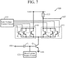
- FIG. 7 is a schematic configuration diagram of a variable gain amplifier 100 of related art disclosed in Patent Literature 1.
- the variable gain amplifier 100 has a digitally controlled current-steering configuration. As illustrated in FIG.
- the variable gain amplifier 100 includes a bipolar transistor Q1 for performing voltage-to-current conversion on a signal input from a signal input terminal 101 via a capacitor C1, a base-current supplying circuit 121 for supplying base current to the bipolar transistor Q1, a signal transmission circuit 111 including a plurality of transistors P 1 to P M , a signal short circuit 110 including a plurality of transistors A 1 to A M , and a gate-voltage control circuit 122 for selectively turning on or off the transistors P 1 to P M , and A 1 to A M .
- the signal transmission circuit 111 is connected between a collector terminal of the bipolar transistor Q1 and the signal output terminal 102, and the signal short circuit 110 is connected between the collector terminal and a supply line of power supply voltage VDD.
- a load resistor 113 is connected between the signal transmission circuit 111 and the supply line of the power supply voltage VDD.
- a ground potential VSS is applied to an emitter of the bipolar transistor Q1.
- a current signal output from the collector terminal of the bipolar transistor Q1 is input to the signal transmission circuit 111 and the signal short circuit 110.
- the gate-voltage control circuit 122 is capable of controlling the total number (total sum of ratios W/L of gate widths W to gate lengths L) of transistors to be in a turned-on states among transistors P 1 to P M , and A 1 to A M by controlling the gate voltage of each of the transistors P 1 to P M , and A 1 to A M .
- the gate-voltage control circuit 122 makes an impedance constant as the signal transmission circuit 111 and the signal short circuit 110 are viewed from the collector terminal of the bipolar transistor Q1, by performing control to allow the value of the denominator np + na of the middle member of the expression to be constant.
- Patent Literature 1 Japanese Patent Application Publication No. 2007-259297 ( FIG. 2 ).
- the current gain Di is determined by a ratio of np and na, which requires a large number of transistors in order to improve gain resolution. With an increased number of transistors, however, the parasitic capacitance is increased, which causes the problem that characteristics of variable gain amplifier are degraded in the high-frequency region.
- variable gain amplifier capable of suppressing deterioration in high-frequency characteristics with a relatively small number of transistors.
- a variable gain amplifier which includes: a signal input port; a signal output port; a signal transmission circuit having an input end connected to the signal input port and an output end connected to the signal output port, and including a plurality of amplifying transistor units which are connected in parallel between the input end and the output end; a load circuit connected between a power supply line and the output end of the signal transmission circuit; a signal short circuit including at least one short-circuit transistor unit which is connected between the power supply line and the input end of the signal transmission circuit; a constant-current source circuit connected to the input end of the signal transmission circuit; and a transistor control circuit configured to select a prescribed number of transistor units to be turned on, from among the amplifying transistor units and the at least one short-circuit transistor unit, and configured to supply one or more control voltages for turning on the selected transistor units.
- variable gain amplifier capable of obtaining high gain resolution with a relatively small number of transistors and having excellent high-frequency characteristics is achieved.
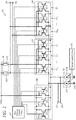
- FIG. 1 is a schematic configuration diagram of a variable gain amplifier 1 that is a first embodiment according to the present invention.
- the variable gain amplifier 1 has a digitally controlled current-steering configuration including a pair of signal input terminals 2P and 2N that receive differential input signals composed of a positive-phase input signal and a negative-phase input signal as a pair thereto, and a pair of signal output terminals 3P and 3N that output differential output signals composed of a positive-phase output signal and a negative-phase output signal as a pair.
- the positive-phase input signal is input to the signal input terminal (first signal input terminal) 2P
- the negative-phase input signal having a negative phase which is an inverse of the phase of the positive-phase input signal
- the signal input terminal (second signal input terminal) 2N is input to the signal input terminal (second signal input terminal) 2N
- the signal output terminal (first signal output terminal) 3P outputs the positive-phase output signal
- the signal input terminal (second signal output terminal) 2N outputs the negative-phase output signal.
- the pair of signal input terminals 2P and 2N constitute a signal input port in the present embodiment
- the pair of signal output terminals 3P and 3N constitute a signal output port in the present embodiment.
- the variable gain amplifier 1 includes a non-inverted signal transmission circuit 10 including N (N is an integer equal to or larger than 3) amplifying transistor units 11 1 to 11 N , an inverted signal transmission circuit 20 including N amplifying transistor units 21 1 to 21 N , and a signal short circuit 30 including a transistor unit 31 for signal line short circuiting. Combination of these non-inverted signal transmission circuit 10 and inverted signal transmission circuit 20 constitutes a signal transmission circuit in the present embodiment.
- the variable gain amplifier 1 also includes a load circuit 40 connected between a supply line for first power supply voltage VDD and an output end of the signal transmission circuit (non-inverted signal transmission circuit 10 and inverted signal transmission circuit 20), a constant-current source circuit 42 connected between a supply line for second power supply voltage VSS (VSS ⁇ VDD) and an input end of the signal transmission circuit, and a gate-voltage control circuit 46 that functions as a transistor control circuit.
- the gate-voltage control circuit 46 selects a combination of transistor units to be turned on from the amplifying transistor units 11 1 to 11 N , and 21 1 to 21 N and the transistor unit 31 for signal line short circuiting, and supplies control voltage for turning on the selected combination of the transistor units to the amplifying transistor units 11 1 to 11 N , 21 1 to 21 N and the transistor unit 31.
- the variable gain of the variable gain amplifier 1 is determined depending on the selected combination of the transistor units.
- the power supply voltage VSS can be a ground potential of zero volts, for example.
- variable gain amplifier 1 includes the constant-current source circuit 42 connected to an input end of the non-inverted signal transmission circuit 10 and an input end of the inverted signal transmission circuit 20, and a current control circuit 45 for variably controlling the amounts of two currents flowing through the constant-current source circuit 42.
- the constant-current source circuit 42 is constituted by two variable constant-current sources 43P and 43N. One end of one variable constant-current source (first constant-current source) 43P is connected to the signal input terminal 2P, and one end of the other variable constant-current source (second constant-current source) 43N is connected to the signal input terminal 2N. The other ends of the variable constant-current sources 43P and 43N are connected to the supply line of the second power supply voltage VSS.
- the current control circuit 45 is capable of variably and individually controlling the amounts of two currents each flowing through the respective one of the variable constant-current sources 43P and 43N.
- the load circuit 40 is constituted by two load resistors 41P and 41N each made of a resistive element.
- the load circuit 40 is connected between the supply line of the first power supply voltage VDD and an output end of the non-inverted signal transmission circuit 10 and between the supply line of the first power supply voltage VDD and the inverted signal transmission circuit 20.
- One end of the load resistor 41P and one end of the load resistor 41N are both connected to the supply line of the first power supply voltage VDD.
- the transistor unit 11 1 to 11 N included in the non-inverted signal transmission circuit 10 are each constituted by a pair of field-effect transistors for signal amplification, and the field-effect transistors (hereinafter, the field-effect transistors will also be simply referred to as "transistors") of each pair are connected in parallel with each other.
- an n-th (n is any integer from 1 to N) transistor unit 11 n is constituted by a pair of amplifying transistors TP n and TN n connected in parallel with each other.
- the amplifying transistors TP n and TN n can be constituted by n-channel metal-oxide -semiconductor field effect transistors (MOSFETs), for example.
- Gates of the amplifying transistors TP n and TN n are both connected to the gate-voltage control circuit 46.
- the gate-voltage control circuit 46 is capable of switching the operation state of each of the amplifying transistors TP n and TN n to either a turned-on state or a turned-off state by applying control voltages to the gates.
- the amplifying transistors TP n and TN n when being turned on are controlled so as to serve as grounded-gate transistors with fixed gate voltages.
- the non-inverted signal transmission circuit 10 includes amplifying transistors TP 1 to TP N constituting a first transistor group connected between the signal input terminal 2P for the positive phase and the signal output terminal 3P for the positive phase, and amplifying transistors TN 1 to TN N constituting a second transistor group connected between the signal input terminal 2N for the negative phase and the signal output terminal 3N for the negative phase. Drains (output ends) of the amplifying transistors TP 1 to TP N are connected to the other end of the load resistor 41P. In addition, drains (output ends) of the amplifying transistors TN 1 to TN N are connected to the other end of the load resistor 41N.
- Sources (input ends) of the amplifying transistors TP 1 to TP N are connected to both of the signal input terminal 2P for the positive phase and one end of the variable constant-current source 43P. Furthermore, sources (input ends) of the amplifying transistors TN 1 to TN N are connected to both of the signal input terminal 2N for the negative phase and one end of the variable constant-current source 43N.
- the transistor unit 21 1 to 21 N included in the inverted signal transmission circuit 20 are each constituted by a pair of transistors for signal amplification, and the transistors of each pair are connected in parallel with each other.
- an n-th transistor unit 21 n is constituted by a pair of amplifying transistors RP n and RN n connected in parallel with each other.
- These amplifying transistors RP n and RN n can be constituted by n-channel MOSFETs, for example.
- Gates of the amplifying transistors RP n and RN n are both connected to the gate-voltage control circuit 46.
- the gate-voltage control circuit 46 is capable of switching the operation state of each of the amplifying transistors RP n and RN n to either a turned-on state or a turned-off state by applying control voltages to the gates.
- the amplifying transistors RP n and RN n when being turned on are controlled to serve as grounded-gate transistors with fixed gate voltages.
- the inverted signal transmission circuit 20 includes amplifying transistors RP 1 to RP N constituting a third transistor group connected between the signal input terminal 2P for the positive phase and the signal output terminal 3N for the negative phase, and amplifying transistors RN 1 to RN N constituting a fourth transistor group connected between the signal input terminal 2N for the negative phase and the signal output terminal 3P for the positive phase. Drains (output ends) of the amplifying transistors RP 1 to RP N are connected to the other end of the load resistor 41N. In addition, drains (output ends) of the amplifying transistors RN 1 to RN N are connected to the other end of the load resistor 41P.
- Sources (input ends) of the amplifying transistors RP 1 to RP N are connected to both of the signal input terminal 2P for the positive phase and one end of the variable constant-current source 43P. Furthermore, sources (input ends) of the amplifying transistors RN 1 to RN N are connected to both of the signal input terminal 2N for the negative phase and one end of the variable constant-current source 43N.
- the signal short circuit 30 is connected between the supply line of the first power supply voltage VDD and the input end of the non-inverted signal transmission circuit 10 and between the supply line of the first power supply voltage VDD and the input end of the inverted signal transmission circuit 20.
- the transistor unit 31 included in the signal short circuit 30 is constituted by a pair of transistors MP and MN connected in parallel with each other.
- a source of one amplifying transistor MP of the pair is connected to the signal input terminal 2P for the positive phase
- a source of the other amplifying transistor MN is connected to the signal input terminal 2N for the negative phase.
- drains of the amplifying transistors MP and MN are both connected to the supply line of the first power supply voltage VDD.
- the transistors MP and MN when being turned on are controlled to serve as grounded-gate transistors with fixed gate voltages.
- the number of transistor unit 11 1 to 11 N included in the non-inverted signal transmission circuit 10 is equal to or larger than three in the configuration of FIG. 1 , the number is not limited thereto, but may be two.
- the number of transistor unit 21 1 to 21 N included in the inverted signal transmission circuit 20 is not limited to be equal to or larger than three, but may be two.
- the number of transistor unit 11 1 to 11 N included in the non-inverted signal transmission circuit 10 and the number of transistor unit 21 1 to 21 N included in the inverted signal transmission circuit 20 are equal in the configuration of FIG. 1 , the numbers are not limited thereto.
- variable gain amplifier 1 Positive-phase and negative-phase signal currents input to the signal input terminals 2P and 2N each flow into the non-inverted signal transmission circuit 10, the inverted signal transmission circuit 20, and the signal short circuit 30. Since the constant-current source circuit 42 is a high impedance circuit that applies a constant amount of current, the signal currents do not flow into the constant-current source circuit 42.
- the gate-voltage control circuit 46 selects a combination of transistor pairs to be turned on depending on a set value of the gain from the transistor pairs included in the non-inverted signal transmission circuit 10, the inverted signal transmission circuit 20, and the signal short circuit 30. The signal currents are amplified with a gain depending on the combination, and output through the signal output terminals 3P and 3N.
- the gate-voltage control circuit 46 can select a combination of transistor pairs to be turned on from the transistor pairs included in each of the non-inverted signal transmission circuit 10 and the inverted signal transmission circuit 20 by using a bit string called a thermometer code, for example.
- a thermometer code is a bit string expressed in binary notation, which is generated by sequentially allocating a value of 1 from the uppermost bit or the lowermost bit. Each of the bits of the thermometer code is associated one-to-one with one of the transistor pair.
- the gate-voltage control circuit 46 can convert the number of transistor pairs to be turned on into a thermometer code, and then generate a control voltage group for turning on transistor pairs associated with bits with a value of 1 (or a value of 0) in the thermometer code and turning off transistor pairs associated with bits with a value of 0 (or a value of 1) in the thermometer code.
- thermometer code having a length of six bits
- use of a thermometer code with a length of six bits allows the gate-voltage control circuit 46 to select a combination of transistor pairs to be turned on from among six transistor pairs.
- np the number of transistor pairs controlled to be in the turned-on states in the non-inverted signal transmission circuit 10
- nn the number of transistor pairs controlled to be in the turned-on states in the inverted signal transmission circuit 20
- na the number of transistor pairs controlled to be in the turned-on states in the signal short circuit 30
- na has a value of zero or one.
- the current gain Bi has a negative value. This means that a signal is output with a negative phase.
- a gain of a high-frequency circuit is often expressed by a power gain, which is a ratio of an input power and an output power.
- Bi described above is not a power gain but a current gain, there is no problem in assuming that a gain of a high-frequency circuit is a current gain as a relative value since the current gain and the power gain satisfy a constant ratio when the input impedance of the circuit is constant.
- the variable gain amplifier 1 of the present embodiment has two kinds of operation modes (a first operation mode and a second operation mode).
- the gate-voltage control circuit 46 always makes constant the sum np + nn + na in the above expression (1), and the current control circuit 45 always makes constant the amount of current flowing through the constant-current source circuit 6.
- g m represents transconductance per unit transistor, the transconductance g m being constant when the amount of current flowing through the unit transistor is constant.
- the input impedance Z in is also a constant value.
- variable gain amplifier 1 When the variable gain amplifier 1 operates in the second operation mode, the gate-voltage control circuit 46 and the current control circuit 45 make constant the product of the sum np + nn + na and the amount of current flowing through the constant-current source circuit 42.
- the transconductance g m is expressed by the following expression (3) with respect to the current Id flowing through a unit transistor: g m ⁇ Id 1 / 2 .
- the transconductance g m is proportional to (Id) 1/2 .
- the input impedance Z in is expressed by the following expression (5): Z in ⁇ 1 / np + nn + na ⁇ I tail 1 / 2 .
- the input impedance Z in can be made constant in such a manner that the amount of current I tail is controlled so that (np + nn + na) ⁇ I tail is constant.
- Example 1 operates in the first operation mode.
- Example 1 is assumed to be a circuit capable of performing variable gain control with a step size of 1 dB within a range of 0 to -15 dB. Note that the number na of transistor pairs included in the signal short circuit 30 is one.
- Example 2 operates in the second operation mode.
- Example 2 is assumed to be a circuit capable of performing variable gain control with a step size of 1 dB within a range of 0 to -15 dB. Note that the number na of transistor pairs included in the signal short circuit 30 is one.
- FIG. 2 is a schematic configuration diagram of a variable gain amplifier 1C that is a comparative example.
- the configuration of the comparative example is the same as that of the variable gain amplifier 1 of the present embodiment except that the signal short circuit 30 in FIG. 1 is replaced by a signal short circuit 30C and that the gate-voltage control circuit 46 in FIG. 1 is replaced by a gate-voltage control circuit 47.
- the number of transistor pairs (transistor units 11 1 to 11 N ) included in the non-inverted signal transmission circuit 10 is 30, and the number of transistor pairs (transistor units 21 1 to 21 N ) included in the inverted signal transmission circuit 20 is also 30.
- na represents the number of transistor pairs in the turned-on states in the signal short circuit 30C.
- the comparative example is assumed to be a circuit capable of performing variable gain control with a step size of 1 dB within a range of 0 to -15 dB.
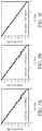
- FIGS. 3A to 3C are graphs illustrating the relation between a set value of gain and a gain that is actually obtained (hereinafter also referred to as "actual gain”).
- the value of the actual gain is a current gain value calculated on the basis of the expression (1) (unit: dB).
- a set value of the gain is given, a combination (np, nn, na) with which an actual gain that is closest to the set value is obtained is selected.
- the horizontal axes of represent the absolute value of the set value of the gain (unit: dB), and the vertical axes represent the value of the actual gain (unit: dB).
- FIG. 3A shows numerical values in the comparative example, FIG.
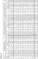
- FIG. 4 is a diagram illustrating a table showing calculated values on which the graphs are based. In the table of FIG. 4 , "total number of differential pairs" represents the total number of transistor pairs.
- the rms value of error of the actual gain (hereinafter referred to as "gain error") with respect to the set value of the gain is 0.30 dB.
- gain error the rms value of error of the actual gain
- an rms value refers to a root mean square value.
- the rms value of the gain error is 0.30 dB, which is approximately the same value as that in the comparative example.
- Example 2 a combination (np, nn, na) with which the gain error is the smallest within a range in which the sum np + nn + na is 30 to 33 is selected. As shown in FIG. 3C , the rms value of the gain error 0.07 dB, which shows that the gain setting accuracy is significantly improved as compared to the comparative example.
- FIG. 5 is a graph showing the relation of the gain accuracy with the total number of transistor pairs (total number of differential pairs).
- the horizontal axis represents the total number of differential pairs
- the vertical axis represents the rms value of the gain error (unit: dB).
- FIG. 5 shows that excellent gain accuracy is achieved even with a smaller number of transistor pairs in the cases of Examples 1 and 2 as compared to the case of the comparative example.
- the number of transistors in Examples 1 and 2 is about two-thirds the number of transistors in the comparative example, gain resolution equivalent to that in the comparative example is achieved.
- parasitic capacitance in Examples 1 and 2 is smaller than that in the comparative example, Examples 1 and 2 achieves better high-frequency characteristics than the comparative example.
- the first embodiment achieves high gain resolution with a relatively small number of transistors, and achieves excellent high-frequency characteristics.
- the transistors TP 1 to TP N , TN 1 to TN N , RP 1 to RP N , and RN 1 to RN N constituting the non-inverted signal transmission circuit 10, the inverted signal transmission circuit 20, and the signal short circuit 30 may be of the same size of W/L (W: gate width, L: gate length) in the present embodiment, the present invention is not limited thereto.
- transistor pairs to be turned on can be selected with use of a binary code.
- the first embodiment is the variable gain amplifier 1 having the function of outputting differential signals having output phases inverted by 180 degrees from each other.
- the present embodiment can be used.
- FIG. 6 is a schematic configuration diagram of a variable gain amplifier 1A that is the second embodiment according to the present invention.
- the variable gain amplifier 1A includes a signal input terminal 4 that receives an input signal thereto, and a signal output terminal 5 that outputs an output signal, and has a configuration to achieve a single-ended input and a single-ended output.
- the signal input terminal 4 constitutes a signal input port in the present embodiment
- the signal output terminal 5 constitutes a signal output port in the present embodiment.
- the variable gain amplifier 1A also includes a signal transmission circuit 23 including N (N is an integer equal to or larger than 3) amplifying transistors R 1 to R N , a signal short circuit 13 including K (K is an integer equal to or larger than 3) short-circuit transistors T 1 to T K , a load resistor 50 constituted by a resistive element connected between a supply line of first power supply voltage VDD and an output end of the signal transmission circuit 23, and a constant-current source circuit 52 connected between a supply line of second power supply voltage VSS (VSS ⁇ VDD) and an input end of the signal transmission circuit 23.
- the power supply voltage VSS can be a ground potential of zero volts, for example.
- the variable gain amplifier 1A also includes a gate-voltage control circuit 56 that functions as a transistor control circuit.
- the gate-voltage control circuit 56 selects a combination of transistors to be turned on, from among the amplifying transistors R 1 to R N and the short-circuit transistors T 1 to T K , and supplies control voltage for turning on the selected combination of the transistors to the amplifying transistors R 1 to R N and the short-circuit transistor T 1 to T K .
- the variable gain of the variable gain amplifier 1A is determined depending on the selected combination of the transistors.
- the amplifying transistors R 1 to R N and the short-circuit transistor T 1 to T K are field-effect transistors, and can be n-channel MOSFETs, for example. Gates of the transistors are connected to the gate-voltage control circuit 56.
- the gate-voltage control circuit 56 is capable of switching the operation state of each of the transistors to either a turned-on state or a turned-off state by applying control voltages to the gates.
- the transistors when being turned on are controlled to serve as grounded-gate transistors with fixed gate voltages.
- the variable gain amplifier 1A further includes a current control circuit 55 that variably controls the amount of current flowing through the constant-current source circuit 52.
- the constant-current source circuit 52 is constituted by one variable constant-current source 53, one end of which is connected to the signal input terminal 4.
- the other end of the variable constant-current source 53 is connected to the supply line of the second power supply voltage VSS.
- the current control circuit 55 is capable of variably controlling the amount of current flowing through the variable constant-current source 53.
- One end of the load resistor 50 is connected to the supply line of the first power supply voltage VDD.
- the other end of the load resistor 50 is connected to drains (output ends) of the amplifying transistors R 1 to R N .
- sources (input ends) of the amplifying transistors R 1 to R N are connected to both of the signal input terminal 4 and one end of the variable constant-current source 53.
- sources of the short-circuit transistor T 1 to T K are also connected to both of the signal input terminal 4 and one end of the variable constant-current source 53, and drains of the short-circuit transistor T 1 to T K are connected to the supply line of the first power supply voltage VDD.
- the number of amplifying transistors R 1 to R N included in the signal transmission circuit 23 is equal to or larger than three in the configuration of FIG. 6 , the number is not limited thereto, but may be two.
- the number of short-circuit transistor T 1 to T N included in the signal short circuit 13 is not limited to be equal to or larger than three, but may be one or two.
- a signal current input to the signal input terminal 4 flows into the signal transmission circuit 23 and the signal short circuit 13. Because the constant-current source circuit 52 is a high impedance circuit that applies a constant current, the signal current does not flow into the constant-current source circuit 52.
- the gate-voltage control circuit 56 selects a combination of transistors to be turned on depending on a set value of the gain, from among transistor groups of the signal transmission circuit 23 and the signal short circuit 13. The signal current is amplified with a gain depending on the combination, and output through the signal output terminal 5.
- the gate-voltage control circuit 56 can select a combination of transistors to be turned on by using a thermometer code, for example.
- np the number of transistors controlled to be in the turned-on states in the signal transmission circuit 23
- na the number of transistors controlled to be in the turned-on states in the signal short circuit 13
- a gain of a high-frequency circuit is often expressed by a power gain, which is a ratio of an input power and an output power.
- Ci described above is not a power gain but a current gain, there is no problem in assuming that a gain of a high-frequency circuit is a current gain as a relative value since the current gain and the power gain satisfy a constant ratio when the input impedance of the circuit is constant. So as to make the input impedance constant, the variable gain amplifier 1A of the present embodiment has two kinds of operation modes (a first operation mode and a second operation mode).
- the gate-voltage control circuit 56 makes constant the sum np + na in the above expression (6), and the current control circuit 55 always makes constant the amount of current flowing through the constant-current source circuit 52.
- g m represents transconductance per unit transistor, the transconductance g m being constant when the current flowing through the unit transistor is constant.
- the input impedance Z in is also a constant value.
- the gate-voltage control circuit 56 and the current control circuit 55 make constant the product of the sum np + na and the amount of current flowing through the constant-current source circuit 52.
- the transconductance g m is expressed by the following expression (8) with respect to the current Id flowing through a unit transistor: g m ⁇ Id 1 / 2 .
- the transconductance g m is proportional to (Id) 1/2 .
- I tail np + na ⁇ Id .
- the input impedance Z in is expressed by the following expression (10): Z in ⁇ 1 / np + na ⁇ I tail 1 / 2 .
- the input impedance Z in can be made constant in such a manner that I tail is controlled so that (np + na) ⁇ I tail is constant.
- variable gain amplifier 1A of the present embodiment has a configuration capable of improving the gain accuracy, similarly to the first embodiment, even with a smaller number of transistors in the signal short circuit 13.
- the variable gain amplifier 1A of the present embodiment is capable of reducing the parasitic capacitance and achieving excellent high-frequency characteristics. High gain resolution is therefore obtained with a relatively small number of transistors, and excellent high-frequency characteristics are achieved.
- the transistors R 1 to R N , and T 1 to T K constituting the signal transmission circuit 23 and the signal short circuit 13 may be of the same size of W/L in the present embodiment, the present invention is not limited thereto.
- transistors to be turned on can be selected with use of a binary code.
- first and second embodiments can be freely combined, any components in the embodiments can be modified, and any components in the embodiments can be omitted within the scope of the present invention.
- a variable gain amplifier according to the present invention is suitable for use in a signal-amplitude control circuit such as a signal amplifier circuit or vector-sum phase shifting circuit of a communication device.
- 1, 1A variable gain amplifiers
- 2P, 2N, 4 signal input terminals
- 3P, 3N, 5 signal output terminals
- 10 non-inverted signal transmission circuits
- 11 1 to 11 N transistor units
- 13 signal short circuit
- 20 inverted signal transmission circuit
- 21 1 to 21 N transistor unit
- 23 signal transmission circuit
- 30 signal short circuit
- 31 transistor unit
- 40 load circuit
- 41P, 41N load resistor
- 42 constant-current source circuit
- 43P, 43N variable constant-current source
- 45 current control circuit
- 46, 47 gate-voltage control circuit
- 50 load
- 52 constant-current source circuit
- 53 constant-current source
- 55 current control circuit
- 56 gate-voltage control circuit
- MP MN: short-circuit transistor.
Landscapes
- Engineering & Computer Science (AREA)
- Power Engineering (AREA)
- Control Of Amplification And Gain Control (AREA)
- Amplifiers (AREA)
Abstract
Description
- The present invention relates to a variable gain amplifier for controlling the amplitude of a signal such as a radio-frequency signal.
- Variable gain amplifiers are used for controlling the amplitudes of transmission signals and received signals in communication devices such as mobile phones. Variable gain amplifiers are also used in phase shifters for controlling the phases of signals. For example, in a vector-sum phase shifter, a variable gain amplifier is used to control the amplitudes of an in-phase signal and a quadrature signal having phases shifted by 90 degrees from each other, and add the resulting two signals to generate an output signal. Control of the respective gains of the in-phase signal and the quadrature signal enables control of the phase of the output signal.
- Such a variable gain amplifier is disclosed in Patent Literature 1 (Japanese Patent Application Publication No.
2007-259297 FIG. 7 is a schematic configuration diagram of avariable gain amplifier 100 of related art disclosed inPatent Literature 1. Thevariable gain amplifier 100 has a digitally controlled current-steering configuration. As illustrated inFIG. 7 , thevariable gain amplifier 100 includes a bipolar transistor Q1 for performing voltage-to-current conversion on a signal input from asignal input terminal 101 via a capacitor C1, a base-current supplying circuit 121 for supplying base current to the bipolar transistor Q1, a signal transmission circuit 111 including a plurality of transistors P1 to PM, a signalshort circuit 110 including a plurality of transistors A1 to AM, and a gate-voltage control circuit 122 for selectively turning on or off the transistors P1 to PM, and A1 to AM. The signal transmission circuit 111 is connected between a collector terminal of the bipolar transistor Q1 and thesignal output terminal 102, and the signalshort circuit 110 is connected between the collector terminal and a supply line of power supply voltage VDD. In addition, aload resistor 113 is connected between the signal transmission circuit 111 and the supply line of the power supply voltage VDD. Furthermore, a ground potential VSS is applied to an emitter of the bipolar transistor Q1. - A current signal output from the collector terminal of the bipolar transistor Q1 is input to the signal transmission circuit 111 and the signal
short circuit 110. The gate-voltage control circuit 122 is capable of controlling the total number (total sum of ratios W/L of gate widths W to gate lengths L) of transistors to be in a turned-on states among transistors P1 to PM, and A1 to AM by controlling the gate voltage of each of the transistors P1 to PM, and A1 to AM. When the number of transistors in the turned-on states in the signal transmission circuit 111 is represented by np, and the number of transistors in the turned-on states in the signalshort circuit 110 is represented by na, a current gain Di can be determined by the following expression:
- The gate-
voltage control circuit 122 makes an impedance constant as the signal transmission circuit 111 and the signalshort circuit 110 are viewed from the collector terminal of the bipolar transistor Q1, by performing control to allow the value of the denominator np + na of the middle member of the expression to be constant. - Patent Literature 1: Japanese Patent Application Publication No.
2007-259297 FIG. 2 ). - In the variable gain amplifier of the related art as described above, the current gain Di is determined by a ratio of np and na, which requires a large number of transistors in order to improve gain resolution. With an increased number of transistors, however, the parasitic capacitance is increased, which causes the problem that characteristics of variable gain amplifier are degraded in the high-frequency region.
- In view of the foregoing, it is an object of the present invention to provide a variable gain amplifier capable of suppressing deterioration in high-frequency characteristics with a relatively small number of transistors.
- In accordance with an aspect of the present invention, there is provided a variable gain amplifier which includes: a signal input port; a signal output port; a signal transmission circuit having an input end connected to the signal input port and an output end connected to the signal output port, and including a plurality of amplifying transistor units which are connected in parallel between the input end and the output end; a load circuit connected between a power supply line and the output end of the signal transmission circuit; a signal short circuit including at least one short-circuit transistor unit which is connected between the power supply line and the input end of the signal transmission circuit; a constant-current source circuit connected to the input end of the signal transmission circuit; and a transistor control circuit configured to select a prescribed number of transistor units to be turned on, from among the amplifying transistor units and the at least one short-circuit transistor unit, and configured to supply one or more control voltages for turning on the selected transistor units.
- According to the present invention, a variable gain amplifier capable of obtaining high gain resolution with a relatively small number of transistors and having excellent high-frequency characteristics is achieved.
-
-
FIG. 1 is a schematic configuration diagram of a variable gain amplifier that is a first embodiment according to the present invention. -
FIG. 2 is a schematic configuration diagram of a variable gain amplifier that is a comparative example. -
FIGS. 3A, 3B and 3C are graphs showing the relation between a set value of gain and an actual gain. -
FIG. 4 is a diagram illustrating a table including numerical values showing the relation between the set value of gain and the actual gain. -
FIG. 5 is a graph showing the relation between the total number of operational pairs and gain accuracy. -
FIG. 6 is a schematic configuration diagram of a variable gain amplifier that is a second embodiment according to the present invention. -
FIG. 7 is a configuration diagram of a variable gain amplifier of related art. - Various embodiments according to the present invention will be described in detail below with reference to the drawings.
-
FIG. 1 is a schematic configuration diagram of avariable gain amplifier 1 that is a first embodiment according to the present invention. As illustrated inFIG. 1 , thevariable gain amplifier 1 has a digitally controlled current-steering configuration including a pair ofsignal input terminals signal output terminals 3P and 3N that output differential output signals composed of a positive-phase output signal and a negative-phase output signal as a pair. The positive-phase input signal is input to the signal input terminal (first signal input terminal) 2P, and the negative-phase input signal having a negative phase, which is an inverse of the phase of the positive-phase input signal, is input to the signal input terminal (second signal input terminal) 2N. In addition, the signal output terminal (first signal output terminal) 3P outputs the positive-phase output signal, and the signal input terminal (second signal output terminal) 2N outputs the negative-phase output signal. Note that the pair ofsignal input terminals signal output terminals 3P and 3N constitute a signal output port in the present embodiment. - As illustrated in
FIG. 1 , thevariable gain amplifier 1 includes a non-invertedsignal transmission circuit 10 including N (N is an integer equal to or larger than 3) amplifyingtransistor units 111 to 11N, an invertedsignal transmission circuit 20 including N amplifyingtransistor units 211 to 21N, and a signalshort circuit 30 including atransistor unit 31 for signal line short circuiting. Combination of these non-invertedsignal transmission circuit 10 and invertedsignal transmission circuit 20 constitutes a signal transmission circuit in the present embodiment. - The
variable gain amplifier 1 also includes aload circuit 40 connected between a supply line for first power supply voltage VDD and an output end of the signal transmission circuit (non-invertedsignal transmission circuit 10 and inverted signal transmission circuit 20), a constant-current source circuit 42 connected between a supply line for second power supply voltage VSS (VSS < VDD) and an input end of the signal transmission circuit, and a gate-voltage control circuit 46 that functions as a transistor control circuit. The gate-voltage control circuit 46 selects a combination of transistor units to be turned on from the amplifyingtransistor units 111 to 11N, and 211 to 21N and thetransistor unit 31 for signal line short circuiting, and supplies control voltage for turning on the selected combination of the transistor units to the amplifyingtransistor units 111 to 11N, 211 to 21N and thetransistor unit 31. As will be described later, the variable gain of thevariable gain amplifier 1 is determined depending on the selected combination of the transistor units. Note that the power supply voltage VSS can be a ground potential of zero volts, for example. - Furthermore, the
variable gain amplifier 1 includes the constant-current source circuit 42 connected to an input end of the non-invertedsignal transmission circuit 10 and an input end of the invertedsignal transmission circuit 20, and acurrent control circuit 45 for variably controlling the amounts of two currents flowing through the constant-current source circuit 42. The constant-current source circuit 42 is constituted by two variable constant-current sources signal input terminal 2P, and one end of the other variable constant-current source (second constant-current source) 43N is connected to thesignal input terminal 2N. The other ends of the variable constant-current sources current control circuit 45 is capable of variably and individually controlling the amounts of two currents each flowing through the respective one of the variable constant-current sources - The
load circuit 40 is constituted by twoload resistors load circuit 40 is connected between the supply line of the first power supply voltage VDD and an output end of the non-invertedsignal transmission circuit 10 and between the supply line of the first power supply voltage VDD and the invertedsignal transmission circuit 20. One end of theload resistor 41P and one end of theload resistor 41N are both connected to the supply line of the first power supply voltage VDD. - The
transistor unit 111 to 11N included in the non-invertedsignal transmission circuit 10 are each constituted by a pair of field-effect transistors for signal amplification, and the field-effect transistors (hereinafter, the field-effect transistors will also be simply referred to as "transistors") of each pair are connected in parallel with each other. Specifically, an n-th (n is any integer from 1 to N)transistor unit 11n is constituted by a pair of amplifying transistors TPn and TNn connected in parallel with each other. The amplifying transistors TPn and TNn can be constituted by n-channel metal-oxide -semiconductor field effect transistors (MOSFETs), for example. - Gates of the amplifying transistors TPn and TNn are both connected to the gate-voltage control circuit 46. The gate-voltage control circuit 46 is capable of switching the operation state of each of the amplifying transistors TPn and TNn to either a turned-on state or a turned-off state by applying control voltages to the gates. The amplifying transistors TPn and TNn when being turned on are controlled so as to serve as grounded-gate transistors with fixed gate voltages.
- In addition, the non-inverted
signal transmission circuit 10 includes amplifying transistors TP1 to TPN constituting a first transistor group connected between thesignal input terminal 2P for the positive phase and thesignal output terminal 3P for the positive phase, and amplifying transistors TN1 to TNN constituting a second transistor group connected between thesignal input terminal 2N for the negative phase and the signal output terminal 3N for the negative phase. Drains (output ends) of the amplifying transistors TP1 to TPN are connected to the other end of theload resistor 41P. In addition, drains (output ends) of the amplifying transistors TN1 to TNN are connected to the other end of theload resistor 41N. Sources (input ends) of the amplifying transistors TP1 to TPN are connected to both of thesignal input terminal 2P for the positive phase and one end of the variable constant-current source 43P. Furthermore, sources (input ends) of the amplifying transistors TN1 to TNN are connected to both of thesignal input terminal 2N for the negative phase and one end of the variable constant-current source 43N. - The
transistor unit 211 to 21N included in the invertedsignal transmission circuit 20 are each constituted by a pair of transistors for signal amplification, and the transistors of each pair are connected in parallel with each other. Specifically, an n-th transistor unit 21n is constituted by a pair of amplifying transistors RPn and RNn connected in parallel with each other. These amplifying transistors RPn and RNn can be constituted by n-channel MOSFETs, for example. - Gates of the amplifying transistors RPn and RNn are both connected to the gate-voltage control circuit 46. The gate-voltage control circuit 46 is capable of switching the operation state of each of the amplifying transistors RPn and RNn to either a turned-on state or a turned-off state by applying control voltages to the gates. The amplifying transistors RPn and RNn when being turned on are controlled to serve as grounded-gate transistors with fixed gate voltages.
- In addition, the inverted
signal transmission circuit 20 includes amplifying transistors RP1 to RPN constituting a third transistor group connected between thesignal input terminal 2P for the positive phase and the signal output terminal 3N for the negative phase, and amplifying transistors RN1 to RNN constituting a fourth transistor group connected between thesignal input terminal 2N for the negative phase and thesignal output terminal 3P for the positive phase. Drains (output ends) of the amplifying transistors RP1 to RPN are connected to the other end of theload resistor 41N. In addition, drains (output ends) of the amplifying transistors RN1 to RNN are connected to the other end of theload resistor 41P. Sources (input ends) of the amplifying transistors RP1 to RPN are connected to both of thesignal input terminal 2P for the positive phase and one end of the variable constant-current source 43P. Furthermore, sources (input ends) of the amplifying transistors RN1 to RNN are connected to both of thesignal input terminal 2N for the negative phase and one end of the variable constant-current source 43N. - The signal
short circuit 30 is connected between the supply line of the first power supply voltage VDD and the input end of the non-invertedsignal transmission circuit 10 and between the supply line of the first power supply voltage VDD and the input end of the invertedsignal transmission circuit 20. Thetransistor unit 31 included in the signalshort circuit 30 is constituted by a pair of transistors MP and MN connected in parallel with each other. A source of one amplifying transistor MP of the pair is connected to thesignal input terminal 2P for the positive phase, and a source of the other amplifying transistor MN is connected to thesignal input terminal 2N for the negative phase. In addition, drains of the amplifying transistors MP and MN are both connected to the supply line of the first power supply voltage VDD. The transistors MP and MN when being turned on are controlled to serve as grounded-gate transistors with fixed gate voltages. - While the number of
transistor unit 111 to 11N included in the non-invertedsignal transmission circuit 10 is equal to or larger than three in the configuration ofFIG. 1 , the number is not limited thereto, but may be two. Similarly, the number oftransistor unit 211 to 21N included in the invertedsignal transmission circuit 20 is not limited to be equal to or larger than three, but may be two. Furthermore, while the number oftransistor unit 111 to 11N included in the non-invertedsignal transmission circuit 10 and the number oftransistor unit 211 to 21N included in the invertedsignal transmission circuit 20 are equal in the configuration ofFIG. 1 , the numbers are not limited thereto. - Next, operation of the
variable gain amplifier 1 will be explained. Positive-phase and negative-phase signal currents input to thesignal input terminals signal transmission circuit 10, the invertedsignal transmission circuit 20, and the signalshort circuit 30. Since the constant-current source circuit 42 is a high impedance circuit that applies a constant amount of current, the signal currents do not flow into the constant-current source circuit 42. The gate-voltage control circuit 46 selects a combination of transistor pairs to be turned on depending on a set value of the gain from the transistor pairs included in the non-invertedsignal transmission circuit 10, the invertedsignal transmission circuit 20, and the signalshort circuit 30. The signal currents are amplified with a gain depending on the combination, and output through thesignal output terminals 3P and 3N. - The gate-voltage control circuit 46 can select a combination of transistor pairs to be turned on from the transistor pairs included in each of the non-inverted
signal transmission circuit 10 and the invertedsignal transmission circuit 20 by using a bit string called a thermometer code, for example. A thermometer code is a bit string expressed in binary notation, which is generated by sequentially allocating a value of 1 from the uppermost bit or the lowermost bit. Each of the bits of the thermometer code is associated one-to-one with one of the transistor pair. The gate-voltage control circuit 46 can convert the number of transistor pairs to be turned on into a thermometer code, and then generate a control voltage group for turning on transistor pairs associated with bits with a value of 1 (or a value of 0) in the thermometer code and turning off transistor pairs associated with bits with a value of 0 (or a value of 1) in the thermometer code. For example, in a case of a thermometer code having a length of six bits, when a number n is given as the number of transistor pairs to be turned on, the thermometer code can have one of the values "000000" (n = 0), "000001" (n = 1), "000011" (n = 2), "000111" (n = 3), "001111" (n = 4), "011111" (n = 5) and "111111" (n = 6). Thus, use of a thermometer code with a length of six bits allows the gate-voltage control circuit 46 to select a combination of transistor pairs to be turned on from among six transistor pairs. - When the number of transistor pairs controlled to be in the turned-on states in the non-inverted
signal transmission circuit 10 is represented by np, the number of transistor pairs controlled to be in the turned-on states in the invertedsignal transmission circuit 20 is represented by nn, and the number of transistor pairs controlled to be in the turned-on states in the signalshort circuit 30 is represented by na, a current gain Bi between thesignal input terminals signal output terminals 3P and 3N is expressed by the following expression (1):
- Note that, since the signal
short circuit 30 includes only one pair of transistors, na has a value of zero or one. In a case of np < nn, the current gain Bi has a negative value. This means that a signal is output with a negative phase. - Note that a gain of a high-frequency circuit is often expressed by a power gain, which is a ratio of an input power and an output power. Although Bi described above is not a power gain but a current gain, there is no problem in assuming that a gain of a high-frequency circuit is a current gain as a relative value since the current gain and the power gain satisfy a constant ratio when the input impedance of the circuit is constant. Thus, so as to make the input impedance constant, the
variable gain amplifier 1 of the present embodiment has two kinds of operation modes (a first operation mode and a second operation mode). - First, the first operation mode will be explained. When the
variable gain amplifier 1 operates in the first operation mode, the gate-voltage control circuit 46 always makes constant the sum np + nn + na in the above expression (1), and thecurrent control circuit 45 always makes constant the amount of current flowing through the constant-current source circuit 6. - In the
variable gain amplifier 1 of the present embodiment, the input impedance Zin is expressed by the following expression (2) when the impedance of the constant-current source circuit 42 is assumed to be ideally infinite:
- In the expression, gm represents transconductance per unit transistor, the transconductance gm being constant when the amount of current flowing through the unit transistor is constant. Thus, when the sum np + nn + na is a constant value, the input impedance Zin is also a constant value. A unit transistor in the present embodiment is each transistor pair having a corresponding size when np = 1, nn = 1, or na = 1.
- Next, the second operation mode will be explained. When the
variable gain amplifier 1 operates in the second operation mode, the gate-voltage control circuit 46 and thecurrent control circuit 45 make constant the product of the sum np + nn + na and the amount of current flowing through the constant-current source circuit 42. - When a simplest model is given, the transconductance gm is expressed by the following expression (3) with respect to the current Id flowing through a unit transistor:

- Thus, the transconductance gm is proportional to (Id)1/2. In addition, when the amounts of two currents flowing through the variable constant-
current sources current source circuit 42 are equal, the following relational expression (4) is satisfied where the amount of current is represented by Itail:
- Thus, the input impedance Zin is expressed by the following expression (5):

- Thus, even in a case where the sum np + nn + na is not constant, the input impedance Zin can be made constant in such a manner that the amount of current Itail is controlled so that (np + nn + na) × Itail is constant.
- The effectiveness of the present embodiment will be explained below with reference to Examples 1 and 2 of the present embodiment and a comparative example. Configurations of Examples 1 and 2 and the comparative example are as described below.
- Example 1 operates in the first operation mode. The number of transistor pairs (
transistor units 111 to 11N) included in the non-invertedsignal transmission circuit 10 is 30 (N = 30), and the number of transistor pairs (transistor units 211 to 21N) included in the invertedsignal transmission circuit 20 is also 30. In addition, Example 1 is assumed to be a circuit capable of performing variable gain control with a step size of 1 dB within a range of 0 to -15 dB. Note that the number na of transistor pairs included in the signalshort circuit 30 is one. - Example 2 operates in the second operation mode. The number of transistor pairs (
transistor units 111 to 11N) included in the non-invertedsignal transmission circuit 10 is 30 (N = 30), and the number of transistor pairs (transistor units 211 to 21N) included in the invertedsignal transmission circuit 20 is also 30. In addition, Example 2 is assumed to be a circuit capable of performing variable gain control with a step size of 1 dB within a range of 0 to -15 dB. Note that the number na of transistor pairs included in the signalshort circuit 30 is one. -
FIG. 2 is a schematic configuration diagram of avariable gain amplifier 1C that is a comparative example. As illustrated inFIG. 2 , the configuration of the comparative example is the same as that of thevariable gain amplifier 1 of the present embodiment except that the signalshort circuit 30 inFIG. 1 is replaced by a signalshort circuit 30C and that the gate-voltage control circuit 46 inFIG. 1 is replaced by a gate-voltage control circuit 47. The signalshort circuit 30C includes 30 (S = 30) transistor pairs, each constituted by transistors MPi and MNi (i = any of 1 to 30) having the same configuration as that of the transistors MP and MN. In addition, in the comparative example, the number of transistor pairs (transistor units 111 to 11N) included in the non-invertedsignal transmission circuit 10 is 30, and the number of transistor pairs (transistor units 211 to 21N) included in the invertedsignal transmission circuit 20 is also 30. The gate-voltage control circuit 47 performs control so that the number (= np + nn + na) of transistor pairs in the turned-on states of the signalshort circuit 30C, the non-invertedsignal transmission circuit 10, and the invertedsignal transmission circuit 20 is always 30. Note that na represents the number of transistor pairs in the turned-on states in the signalshort circuit 30C. Furthermore, the comparative example is assumed to be a circuit capable of performing variable gain control with a step size of 1 dB within a range of 0 to -15 dB. -
FIGS. 3A to 3C are graphs illustrating the relation between a set value of gain and a gain that is actually obtained (hereinafter also referred to as "actual gain"). The value of the actual gain is a current gain value calculated on the basis of the expression (1) (unit: dB). When a set value of the gain is given, a combination (np, nn, na) with which an actual gain that is closest to the set value is obtained is selected. In the graphs ofFIGS. 3A to 3C , the horizontal axes of represent the absolute value of the set value of the gain (unit: dB), and the vertical axes represent the value of the actual gain (unit: dB). In addition,FIG. 3A shows numerical values in the comparative example,FIG. 3B shows numerical values in Example 1, andFIG. 3C shows numerical values in Example 2.FIG. 4 is a diagram illustrating a table showing calculated values on which the graphs are based. In the table ofFIG. 4 , "total number of differential pairs" represents the total number of transistor pairs. - In the case of the comparative example, as shown in
FIG. 3A , the rms value of error of the actual gain (hereinafter referred to as "gain error") with respect to the set value of the gain is 0.30 dB. Note that an rms value refers to a root mean square value. In contrast, in the case of Example 1, as shown inFIG. 3B , the rms value of the gain error is 0.30 dB, which is approximately the same value as that in the comparative example. This shows that, although the number of transistor pairs (total number of differential pairs) in Example 1 is about two-thirds the number of transistor pairs (total number of differential pairs) in the comparative example, Example 1 achieves the characteristics equivalent to those in the comparative example. In addition, in the case of Example 2, a combination (np, nn, na) with which the gain error is the smallest within a range in which the sum np + nn + na is 30 to 33 is selected. As shown inFIG. 3C , the rms value of the gain error 0.07 dB, which shows that the gain setting accuracy is significantly improved as compared to the comparative example. -
FIG. 5 is a graph showing the relation of the gain accuracy with the total number of transistor pairs (total number of differential pairs). In the graph ofFIG. 5 , the horizontal axis represents the total number of differential pairs, and the vertical axis represents the rms value of the gain error (unit: dB).FIG. 5 shows that excellent gain accuracy is achieved even with a smaller number of transistor pairs in the cases of Examples 1 and 2 as compared to the case of the comparative example. Thus, in the cases of Examples 1 and 2, although the number of transistors in Examples 1 and 2 is about two-thirds the number of transistors in the comparative example, gain resolution equivalent to that in the comparative example is achieved. In addition, since parasitic capacitance in Examples 1 and 2 is smaller than that in the comparative example, Examples 1 and 2 achieves better high-frequency characteristics than the comparative example. - As described above, the first embodiment achieves high gain resolution with a relatively small number of transistors, and achieves excellent high-frequency characteristics.
- While the transistors TP1 to TPN, TN1 to TNN, RP1 to RPN, and RN1 to RNN constituting the non-inverted
signal transmission circuit 10, the invertedsignal transmission circuit 20, and the signalshort circuit 30 may be of the same size of W/L (W: gate width, L: gate length) in the present embodiment, the present invention is not limited thereto. For example, the circuit configurations of the non-invertedsignal transmission circuit 10 and the invertedsignal transmission circuit 20 may be changed such that the non-invertedsignal transmission circuit 10 and the invertedsignal transmission circuit 20 are constituted by a plurality of transistor pairs whose sizes are powers of 2 (= 2°, 21, 22, 23, ...) times as large as a reference value of W/L. In this case, transistor pairs to be turned on can be selected with use of a binary code. - Next, a second embodiment according to the present invention will be described. The first embodiment is the
variable gain amplifier 1 having the function of outputting differential signals having output phases inverted by 180 degrees from each other. In a case where the function of phase inversion is not necessary, the present embodiment can be used.FIG. 6 is a schematic configuration diagram of a variable gain amplifier 1A that is the second embodiment according to the present invention. - As illustrated in
FIG. 6 , the variable gain amplifier 1A includes asignal input terminal 4 that receives an input signal thereto, and asignal output terminal 5 that outputs an output signal, and has a configuration to achieve a single-ended input and a single-ended output. Note that thesignal input terminal 4 constitutes a signal input port in the present embodiment, and thesignal output terminal 5 constitutes a signal output port in the present embodiment. - The variable gain amplifier 1A also includes a
signal transmission circuit 23 including N (N is an integer equal to or larger than 3) amplifying transistors R1 to RN, a signalshort circuit 13 including K (K is an integer equal to or larger than 3) short-circuit transistors T1 to TK, aload resistor 50 constituted by a resistive element connected between a supply line of first power supply voltage VDD and an output end of thesignal transmission circuit 23, and a constant-current source circuit 52 connected between a supply line of second power supply voltage VSS (VSS < VDD) and an input end of thesignal transmission circuit 23. The power supply voltage VSS can be a ground potential of zero volts, for example. - The variable gain amplifier 1A also includes a gate-
voltage control circuit 56 that functions as a transistor control circuit. The gate-voltage control circuit 56 selects a combination of transistors to be turned on, from among the amplifying transistors R1 to RN and the short-circuit transistors T1 to TK, and supplies control voltage for turning on the selected combination of the transistors to the amplifying transistors R1 to RN and the short-circuit transistor T1 to TK. The variable gain of the variable gain amplifier 1A is determined depending on the selected combination of the transistors. - The amplifying transistors R1 to RN and the short-circuit transistor T1 to TK are field-effect transistors, and can be n-channel MOSFETs, for example. Gates of the transistors are connected to the gate-
voltage control circuit 56. The gate-voltage control circuit 56 is capable of switching the operation state of each of the transistors to either a turned-on state or a turned-off state by applying control voltages to the gates. The transistors when being turned on are controlled to serve as grounded-gate transistors with fixed gate voltages. - The variable gain amplifier 1A further includes a
current control circuit 55 that variably controls the amount of current flowing through the constant-current source circuit 52. The constant-current source circuit 52 is constituted by one variable constant-current source 53, one end of which is connected to thesignal input terminal 4. The other end of the variable constant-current source 53 is connected to the supply line of the second power supply voltage VSS. Thecurrent control circuit 55 is capable of variably controlling the amount of current flowing through the variable constant-current source 53. - One end of the
load resistor 50 is connected to the supply line of the first power supply voltage VDD. The other end of theload resistor 50 is connected to drains (output ends) of the amplifying transistors R1 to RN. In addition, sources (input ends) of the amplifying transistors R1 to RN are connected to both of thesignal input terminal 4 and one end of the variable constant-current source 53. In addition, sources of the short-circuit transistor T1 to TK are also connected to both of thesignal input terminal 4 and one end of the variable constant-current source 53, and drains of the short-circuit transistor T1 to TK are connected to the supply line of the first power supply voltage VDD. - While the number of amplifying transistors R1 to RN included in the
signal transmission circuit 23 is equal to or larger than three in the configuration ofFIG. 6 , the number is not limited thereto, but may be two. Similarly, the number of short-circuit transistor T1 to TN included in the signalshort circuit 13 is not limited to be equal to or larger than three, but may be one or two. - Next, operation of the variable gain amplifier 1A will be explained. A signal current input to the
signal input terminal 4 flows into thesignal transmission circuit 23 and the signalshort circuit 13. Because the constant-current source circuit 52 is a high impedance circuit that applies a constant current, the signal current does not flow into the constant-current source circuit 52. The gate-voltage control circuit 56 selects a combination of transistors to be turned on depending on a set value of the gain, from among transistor groups of thesignal transmission circuit 23 and the signalshort circuit 13. The signal current is amplified with a gain depending on the combination, and output through thesignal output terminal 5. Similarly to the gate-voltage control circuit 46 of the first embodiment, the gate-voltage control circuit 56 can select a combination of transistors to be turned on by using a thermometer code, for example. - When the number of transistors controlled to be in the turned-on states in the
signal transmission circuit 23 is represented by np, and the number of transistors controlled to be in the turned-on states in the signalshort circuit 13 is represented by na, a current gain Ci between thesignal input terminal 4 and thesignal output terminal 5 is expressed by the following expression (6):
- Note that, as mentioned above, a gain of a high-frequency circuit is often expressed by a power gain, which is a ratio of an input power and an output power. Although Ci described above is not a power gain but a current gain, there is no problem in assuming that a gain of a high-frequency circuit is a current gain as a relative value since the current gain and the power gain satisfy a constant ratio when the input impedance of the circuit is constant. So as to make the input impedance constant, the variable gain amplifier 1A of the present embodiment has two kinds of operation modes (a first operation mode and a second operation mode).
- When the variable gain amplifier 1A operates in the first operation mode, the gate-
voltage control circuit 56 makes constant the sum np + na in the above expression (6), and thecurrent control circuit 55 always makes constant the amount of current flowing through the constant-current source circuit 52. - In the variable gain amplifier 1A of the present embodiment, the input impedance Zin is expressed by the following expression (7) when the impedance of the constant-
current source circuit 52 is assumed to be ideally infinite:
- In the expression, gm represents transconductance per unit transistor, the transconductance gm being constant when the current flowing through the unit transistor is constant. Thus, when the sum np + na is a constant value, the input impedance Zin is also a constant value. A unit transistor in the present embodiment is each transistor having a corresponding size when np = 1 or na = 1.
- Next, when the variable gain amplifier 1A operates in the second operation mode, the gate-
voltage control circuit 56 and thecurrent control circuit 55 make constant the product of the sum np + na and the amount of current flowing through the constant-current source circuit 52. - When a simplest model is given, the transconductance gm is expressed by the following expression (8) with respect to the current Id flowing through a unit transistor:

- Thus, the transconductance gm is proportional to (Id)1/2. In addition, when the amount of current flowing through the constant-
current source circuit 52 is represented by Itail, the following relational expression (9) is satisfied:
- Thus, the input impedance Zin is expressed by the following expression (10):

- Thus, even when the sum np + na is not constant, the input impedance Zin can be made constant in such a manner that Itail is controlled so that (np + na) × Itail is constant.
- As described above, the variable gain amplifier 1A of the present embodiment has a configuration capable of improving the gain accuracy, similarly to the first embodiment, even with a smaller number of transistors in the signal
short circuit 13. Thus, even with gain resolution equivalent to that in the related art, the variable gain amplifier 1A of the present embodiment is capable of reducing the parasitic capacitance and achieving excellent high-frequency characteristics. High gain resolution is therefore obtained with a relatively small number of transistors, and excellent high-frequency characteristics are achieved. - While the transistors R1 to RN, and T1 to TK constituting the
signal transmission circuit 23 and the signalshort circuit 13 may be of the same size of W/L in the present embodiment, the present invention is not limited thereto. For example, the circuit configurations of thesignal transmission circuit 23 and the signalshort circuit 13 may be changed such that thesignal transmission circuit 23 and the signalshort circuit 13 are constituted by a plurality of transistors whose sizes are powers of 2 (= 20, 21, 22, 23, ...) times as large as a reference value of W/L. In this case, transistors to be turned on can be selected with use of a binary code. - Various embodiments according to the present invention have been described above with reference to the drawings; these embodiments, however, are merely examples of the present invention and various forms other than these embodiments may also be adopted. For example, while field-effect transistors are used for transistors constituting the non-inverted
signal transmission circuit 10, the invertedsignal transmission circuit 20, and the signalshort circuit 30 in the first embodiment, the transistors are not limited thereto. Similarly, while field-effect transistors are used for transistors constituting thesignal transmission circuit 23 and the signalshort circuit 13 in the second embodiment, the transistors are not limited thereto. The configurations of the first and second embodiments may be changed so that the field-effect transistors are replaced by bipolar transistors. - Note that the first and second embodiments can be freely combined, any components in the embodiments can be modified, and any components in the embodiments can be omitted within the scope of the present invention.
- A variable gain amplifier according to the present invention is suitable for use in a signal-amplitude control circuit such as a signal amplifier circuit or vector-sum phase shifting circuit of a communication device.
- 1, 1A: variable gain amplifiers; 2P, 2N, 4: signal input terminals; 3P, 3N, 5: signal output terminals; 10: non-inverted signal transmission circuits; 111 to 11N: transistor units; 13: signal short circuit; 20: inverted signal transmission circuit; 211 to 21N: transistor unit; 23: signal transmission circuit; 30: signal short circuit; 31: transistor unit; 40: load circuit; 41P, 41N: load resistor; 42: constant-current source circuit; 43P, 43N: variable constant-current source; 45: current control circuit; 46, 47: gate-voltage control circuit; 50: load; 52: constant-current source circuit; 53: constant-current source; 55: current control circuit; 56: gate-voltage control circuit; RP1 to RPN, RN1 to RNN, TP1 to TPN, TN1 to TNN: amplifying transistor; and MP, MN: short-circuit transistor.
Claims (12)
- A variable gain amplifier comprising:a signal input port;a signal output port;a signal transmission circuit having an input end connected to the signal input port and an output end connected to the signal output port, and including a plurality of amplifying transistor units which are connected in parallel between the input end and the output end;a load circuit connected between a power supply line and the output end of the signal transmission circuit;a signal short circuit including at least one short-circuit transistor unit which is connected between the power supply line and the input end of the signal transmission circuit;a constant-current source circuit connected to the input end of the signal transmission circuit; anda transistor control circuit configured to select a prescribed number of transistor units to be turned on, from among the amplifying transistor units and the at least one short-circuit transistor unit, and configured to supply one or more control voltages for turning on the selected transistor units.
- The variable gain amplifier according to claim 1, wherein each of the at least one short-circuit transistor unit and the amplifying transistor units includes a pair of transistors which are connected in parallel with each other.
- The variable gain amplifier according to claim 2, wherein the pairs of transistors when being turned on are controlled to be transistors with grounded gates.
- The variable gain amplifier according to claim 2, wherein:the signal input port includes a first signal input terminal for receiving a positive-phase input signal thereto, and a second signal input terminal for receiving a negative-phase input signal thereto;the signal output port includes a first signal output terminal for outputting a positive-phase output signal, and a second signal output terminal for outputting a negative-phase output signal;the signal transmission circuit includesa non-inverted signal transmission circuit including, as a part of the plurality of amplifying transistor units, a first transistor group connected in parallel between the first signal input terminal and the first signal output terminal, and a second transistor group connected in parallel between the second signal input terminal and the second signal input terminal, andan inverted signal transmission circuit including, as another part of the plurality of amplifying transistor units, a third transistor group connected in parallel between the first signal input terminal and the second signal output terminal, and a fourth transistor group connected in parallel between the second signal input terminal and the first signal input terminal;the load circuit includesa first load resistor connected between an output end of the first transistor group and the power supply line and between an output end of the third transistor group and the power supply line, anda second load resistor connected between an output end of the second transistor group and the power supply line and between an output end of the fourth transistor group and the power supply line; andthe constant-current source circuit includes a first constant-current source connected to an input end of the first transistor group and an input end of the third transistor group, and a second constant-current source connected to an input end of the second transistor group and an input end of the fourth transistor group.
- The variable gain amplifier according to claim 1, wherein:the plurality of amplifying transistor units includes a plurality of amplifying transistors connected in parallel with each other;an input end of each of the amplifying transistors is connected to the signal input port, and an output end of each of the amplifying transistors is connected to the signal output port;the at least one short-circuit transistor unit includes a plurality of short-circuit transistors connected in parallel with each other;an input end of each of the short-circuit transistors is connected to the signal input port, and an output end of each of the short-circuit transistors is connected to the power supply line; andthe constant-current source circuit is connected to the input end of each of the amplifying transistors and the input end of each of the short-circuit transistors.
- The variable gain amplifier according to claim 5, wherein: each of the amplifying transistors when being turned on is controlled to be a transistor with a grounded gate; and each of the short-circuit transistors when being turned on is controlled to be a transistor with a grounded gate.
- A variable gain amplifier comprising:a signal input port;a signal output port;a signal transmission circuit having an input end connected to the signal input port and an output end connected to the signal output port, and including a plurality of amplifying transistor units connected in parallel between the input end and the output end;a load circuit connected between a power supply line and the output end of the signal transmission circuit;a signal short circuit including at least one short-circuit transistor unit which is connected between the power supply line and the input end of the signal transmission circuit;a constant-current source circuit connected to the input end of the signal transmission circuit;a transistor control circuit configured to select transistor units to be turned on, from among the amplifying transistor units and the at least one short-circuit transistor unit, and configured to supply one or more control voltages for turning on the selected transistor units; anda current control circuit configured to variably control an amount of current flowing through the constant-current source circuit to allow a product of the amount of current and a total number of the selected transistor units to be constant.
- The variable gain amplifier according to claim 7, wherein each of the amplifying transistor units and the at least one short-circuit transistor unit includes a pair of transistors which are connected in parallel with each other.
- The variable gain amplifier according to claim 8, wherein the pairs of transistors when being turned on are controlled to be transistors with grounded gates.
- The variable gain amplifier according to claim 8, wherein:the signal input port includes a first signal input terminal for receiving a positive-phase input signal thereto, and a second signal input terminal receiving a negative-phase input signal thereto;the signal output port includes a first signal output terminal for outputting a positive-phase output signal, and a second signal output terminal for outputting a negative-phase output signal;the signal transmission circuit includesa non-inverted signal transmission circuit including, as a part of the plurality of amplifying transistor units, a first transistor group connected in parallel between the first signal input terminal and the first signal output terminal, and a second transistor group connected in parallel between the second signal input terminal and the second signal input terminal, andan inverted signal transmission circuit including, as another part of the plurality of amplifying transistor units, a third transistor group connected in parallel between the first signal input terminal and the second signal output terminal, and a fourth transistor group connected in parallel between the second signal input terminal and the first signal input terminal;the load circuit includesa first load resistor connected between an output end of the first transistor group and the power supply line and between an output end of the third transistor group and the power supply line, anda second load resistor connected between an output end of the second transistor group and the power supply line and between an output end of the fourth transistor group and the power supply line;the constant-current source circuit includes a first variable constant-current source connected to an input end of the first transistor group and an input end of the third transistor group, and a second variable constant-current source connected to an input end of the second transistor group and an input end of the fourth transistor group; andthe current control circuit variably controls a first amount of current flowing through the first variable constant-current source to allow a product of the first amount of current and a total number of transistor units selected by the transistor control circuit to be constant, and variably controls a second amount of current flowing through the second variable constant-current source to allow a product of the second amount of current and the total number of selected transistor units to be constant.
- The variable gain amplifier according to claim 7, wherein:the plurality of amplifying transistor units includes a plurality of amplifying transistors connected in parallel with each other;an input end of each of the amplifying transistors is connected to the signal input port, and an output end of each of the amplifying transistors is connected to the signal output port;the at least one short-circuit transistor unit includes a plurality of short-circuit transistors connected in parallel with each other;an input end of each of the short-circuit transistors is connected to the signal input port, and an output end of each of the short-circuit transistors is connected to the power supply line; andthe constant-current source circuit is connected to the input end of each of the amplifying transistors and the input end of each of the short-circuit transistors.
- The variable gain amplifier according to claim 11, wherein: each of the amplifying transistors when being turned on is controlled to be a transistor with a grounded gate; and each of the short-circuit transistors when being turned on is controlled to be a transistor with a grounded gate.
Applications Claiming Priority (1)
| Application Number | Priority Date | Filing Date | Title |
|---|---|---|---|
| PCT/JP2016/059193 WO2017163334A1 (en) | 2016-03-23 | 2016-03-23 | Variable gain amplifier |
Publications (3)
| Publication Number | Publication Date |
|---|---|
| EP3419164A1 true EP3419164A1 (en) | 2018-12-26 |
| EP3419164A4 EP3419164A4 (en) | 2019-03-13 |
| EP3419164B1 EP3419164B1 (en) | 2020-06-03 |
Family
ID=57937611
Family Applications (1)
| Application Number | Title | Priority Date | Filing Date |
|---|---|---|---|
| EP16895370.1A Not-in-force EP3419164B1 (en) | 2016-03-23 | 2016-03-23 | Variable gain amplifier |
Country Status (5)
| Country | Link |
|---|---|
| US (1) | US10581395B2 (en) |
| EP (1) | EP3419164B1 (en) |
| JP (1) | JP6072387B1 (en) |
| CN (1) | CN108781062B (en) |
| WO (1) | WO2017163334A1 (en) |
Families Citing this family (2)
| Publication number | Priority date | Publication date | Assignee | Title |
|---|---|---|---|---|
| CN112514249B (en) * | 2018-08-10 | 2024-10-22 | 三菱电机株式会社 | Variable Gain Amplifier |
| JP7221668B2 (en) * | 2018-12-04 | 2023-02-14 | ルネサスエレクトロニクス株式会社 | semiconductor equipment |
Family Cites Families (18)
| Publication number | Priority date | Publication date | Assignee | Title |
|---|---|---|---|---|
| US7120411B2 (en) * | 2002-03-25 | 2006-10-10 | Broadcom Corporation | Low noise amplifier (LNA) gain switch circuitry |
| JP2003234627A (en) * | 2002-02-08 | 2003-08-22 | Toyota Industries Corp | Semiconductor circuit |
| JP4095398B2 (en) * | 2002-09-30 | 2008-06-04 | 株式会社東芝 | Amplifier and radio communication apparatus using the same |
| DE10333816B3 (en) * | 2003-07-24 | 2005-03-10 | Infineon Technologies Ag | Amplifier arrangement and control circuit with the amplifier arrangement |
| JP2005123821A (en) * | 2003-10-15 | 2005-05-12 | Alps Electric Co Ltd | Variable gain amplifier |
| US7321266B2 (en) * | 2005-05-17 | 2008-01-22 | Integrated System Solution Corp. | Current-matching variable gain amplifier |
| JP4502212B2 (en) | 2006-01-06 | 2010-07-14 | ルネサスエレクトロニクス株式会社 | Differential amplifier, data driver and display device |
| JP2007221402A (en) | 2006-02-16 | 2007-08-30 | Fujitsu Ltd | Variable gain amplifier and semiconductor integrated device thereof |
| JP4354465B2 (en) | 2006-03-24 | 2009-10-28 | シャープ株式会社 | Variable gain amplifier and communication apparatus including the variable gain amplifier |
| EP1858160A1 (en) * | 2006-05-16 | 2007-11-21 | STMicroelectronics (Research & Development) Limited | Amplifier arrangement |
| WO2008102788A1 (en) | 2007-02-20 | 2008-08-28 | Nagoya Industrial Science Research Institute | Programmable low-noise amplifier |
| JP2009089225A (en) | 2007-10-02 | 2009-04-23 | Toshiba Corp | Variable gain amplifier |
| JP5308243B2 (en) | 2009-06-10 | 2013-10-09 | 株式会社日立製作所 | Variable gain circuit |
| KR101787761B1 (en) * | 2011-08-09 | 2017-10-18 | 삼성전자주식회사 | Rf amplifier |
| JP5743850B2 (en) * | 2011-10-28 | 2015-07-01 | 株式会社東芝 | Integrated circuit |
| TWI469511B (en) * | 2011-12-07 | 2015-01-11 | Novatek Microelectronics Corp | Variable gain amplifier circuit |
| CN102684622B (en) * | 2012-05-24 | 2015-06-10 | 电子科技大学 | Variable gain amplifier |
| US9112472B2 (en) * | 2013-12-16 | 2015-08-18 | Mstar Semiconductor, Inc. | Variable gain low-noise amplifier |
-
2016
- 2016-03-23 WO PCT/JP2016/059193 patent/WO2017163334A1/en not_active Ceased
- 2016-03-23 JP JP2016553909A patent/JP6072387B1/en active Active
- 2016-03-23 EP EP16895370.1A patent/EP3419164B1/en not_active Not-in-force
- 2016-03-23 CN CN201680083617.1A patent/CN108781062B/en not_active Expired - Fee Related
- 2016-03-23 US US16/085,953 patent/US10581395B2/en active Active
Also Published As
| Publication number | Publication date |
|---|---|
| WO2017163334A1 (en) | 2017-09-28 |
| EP3419164B1 (en) | 2020-06-03 |
| JPWO2017163334A1 (en) | 2018-04-05 |
| EP3419164A4 (en) | 2019-03-13 |
| US20190089318A1 (en) | 2019-03-21 |
| JP6072387B1 (en) | 2017-02-01 |
| CN108781062B (en) | 2022-04-12 |
| US10581395B2 (en) | 2020-03-03 |
| CN108781062A (en) | 2018-11-09 |
Similar Documents
| Publication | Publication Date | Title |
|---|---|---|
| CN109347454B (en) | A continuously variable gain amplifier | |
| US20160072460A1 (en) | Differential amplifier | |
| US8410846B2 (en) | Variable gain amplifier | |
| US10530384B2 (en) | Wireless-transmitter circuits including power digital-to-amplitude converters | |
| CN101447785B (en) | Differential drive circuit and communication device | |
| US6784737B2 (en) | Voltage multiplier circuit | |
| US9503022B2 (en) | Balanced up-conversion mixer | |
| US9214898B2 (en) | Triple cascode power amplifier | |
| US20130027017A1 (en) | Voltage to current converting circuit | |
| US20110133837A1 (en) | Variable gain amplifier | |
| CN106464222B (en) | Programmable Gain Amplifier PGA and Programmable Resistor Network Circuit | |
| EP3419164B1 (en) | Variable gain amplifier | |
| US7868695B2 (en) | Differential amplifier | |
| US9477245B1 (en) | High performance voltage-to-current converter for LTE transmitter | |
| US10700652B2 (en) | Ethernet line driver | |
| CN105450240A (en) | Direct digital radio frequency modulator | |
| US9641127B1 (en) | Operational transconductance amplifier of improved linearity | |
| EP3358744B1 (en) | Transconductance amplifier and phase shifter | |
| RU2446554C1 (en) | Differential operational amplifier with paraphase output | |
| CN104617899A (en) | differential amplifier and electronic device | |
| US11502656B2 (en) | Variable gain amplifier | |
| US10826451B2 (en) | Combined resistance circuit and variable gain amplifier circuit | |
| CN110534068B (en) | Driving voltage generator | |
| Purighalla et al. | 4-bit parallel-input exponential digital-to-analog converter in CMOS 0.18 μm technology | |
| KR20230116932A (en) | Linear class AB voltage to current converter |
Legal Events
| Date | Code | Title | Description |
|---|---|---|---|
| STAA | Information on the status of an ep patent application or granted ep patent |
Free format text: STATUS: THE INTERNATIONAL PUBLICATION HAS BEEN MADE |
|
| PUAI | Public reference made under article 153(3) epc to a published international application that has entered the european phase |
Free format text: ORIGINAL CODE: 0009012 |
|
| STAA | Information on the status of an ep patent application or granted ep patent |
Free format text: STATUS: REQUEST FOR EXAMINATION WAS MADE |
|
| 17P | Request for examination filed |
Effective date: 20180912 |
|
| AK | Designated contracting states |
Kind code of ref document: A1 Designated state(s): AL AT BE BG CH CY CZ DE DK EE ES FI FR GB GR HR HU IE IS IT LI LT LU LV MC MK MT NL NO PL PT RO RS SE SI SK SM TR |
|
| AX | Request for extension of the european patent |
Extension state: BA ME |
|
| A4 | Supplementary search report drawn up and despatched |
Effective date: 20190212 |
|
| RIC1 | Information provided on ipc code assigned before grant |
Ipc: H03G 1/00 20060101ALI20190206BHEP Ipc: H03F 3/45 20060101ALI20190206BHEP Ipc: H03G 3/10 20060101AFI20190206BHEP |
|
| DAV | Request for validation of the european patent (deleted) | ||
| DAX | Request for extension of the european patent (deleted) | ||
| GRAP | Despatch of communication of intention to grant a patent |
Free format text: ORIGINAL CODE: EPIDOSNIGR1 |
|
| STAA | Information on the status of an ep patent application or granted ep patent |
Free format text: STATUS: GRANT OF PATENT IS INTENDED |
|
| INTG | Intention to grant announced |
Effective date: 20191219 |
|
| GRAS | Grant fee paid |
Free format text: ORIGINAL CODE: EPIDOSNIGR3 |
|
| GRAA | (expected) grant |
Free format text: ORIGINAL CODE: 0009210 |
|
| STAA | Information on the status of an ep patent application or granted ep patent |
Free format text: STATUS: THE PATENT HAS BEEN GRANTED |
|
| AK | Designated contracting states |
Kind code of ref document: B1 Designated state(s): AL AT BE BG CH CY CZ DE DK EE ES FI FR GB GR HR HU IE IS IT LI LT LU LV MC MK MT NL NO PL PT RO RS SE SI SK SM TR |
|
| REG | Reference to a national code |
Ref country code: GB Ref legal event code: FG4D |
|
| REG | Reference to a national code |
Ref country code: CH Ref legal event code: EP Ref country code: AT Ref legal event code: REF Ref document number: 1278085 Country of ref document: AT Kind code of ref document: T Effective date: 20200615 |
|
| REG | Reference to a national code |
Ref country code: DE Ref legal event code: R096 Ref document number: 602016037744 Country of ref document: DE |
|
| REG | Reference to a national code |
Ref country code: LT Ref legal event code: MG4D |
|
| PG25 | Lapsed in a contracting state [announced via postgrant information from national office to epo] |
Ref country code: LT Free format text: LAPSE BECAUSE OF FAILURE TO SUBMIT A TRANSLATION OF THE DESCRIPTION OR TO PAY THE FEE WITHIN THE PRESCRIBED TIME-LIMIT Effective date: 20200603 Ref country code: FI Free format text: LAPSE BECAUSE OF FAILURE TO SUBMIT A TRANSLATION OF THE DESCRIPTION OR TO PAY THE FEE WITHIN THE PRESCRIBED TIME-LIMIT Effective date: 20200603 Ref country code: NO Free format text: LAPSE BECAUSE OF FAILURE TO SUBMIT A TRANSLATION OF THE DESCRIPTION OR TO PAY THE FEE WITHIN THE PRESCRIBED TIME-LIMIT Effective date: 20200903 Ref country code: GR Free format text: LAPSE BECAUSE OF FAILURE TO SUBMIT A TRANSLATION OF THE DESCRIPTION OR TO PAY THE FEE WITHIN THE PRESCRIBED TIME-LIMIT Effective date: 20200904 Ref country code: SE Free format text: LAPSE BECAUSE OF FAILURE TO SUBMIT A TRANSLATION OF THE DESCRIPTION OR TO PAY THE FEE WITHIN THE PRESCRIBED TIME-LIMIT Effective date: 20200603 |
|
| REG | Reference to a national code |
Ref country code: NL Ref legal event code: MP Effective date: 20200603 |
|
| PG25 | Lapsed in a contracting state [announced via postgrant information from national office to epo] |
Ref country code: HR Free format text: LAPSE BECAUSE OF FAILURE TO SUBMIT A TRANSLATION OF THE DESCRIPTION OR TO PAY THE FEE WITHIN THE PRESCRIBED TIME-LIMIT Effective date: 20200603 Ref country code: RS Free format text: LAPSE BECAUSE OF FAILURE TO SUBMIT A TRANSLATION OF THE DESCRIPTION OR TO PAY THE FEE WITHIN THE PRESCRIBED TIME-LIMIT Effective date: 20200603 Ref country code: BG Free format text: LAPSE BECAUSE OF FAILURE TO SUBMIT A TRANSLATION OF THE DESCRIPTION OR TO PAY THE FEE WITHIN THE PRESCRIBED TIME-LIMIT Effective date: 20200903 Ref country code: LV Free format text: LAPSE BECAUSE OF FAILURE TO SUBMIT A TRANSLATION OF THE DESCRIPTION OR TO PAY THE FEE WITHIN THE PRESCRIBED TIME-LIMIT Effective date: 20200603 |
|
| REG | Reference to a national code |
Ref country code: AT Ref legal event code: MK05 Ref document number: 1278085 Country of ref document: AT Kind code of ref document: T Effective date: 20200603 |
|
| PG25 | Lapsed in a contracting state [announced via postgrant information from national office to epo] |
Ref country code: AL Free format text: LAPSE BECAUSE OF FAILURE TO SUBMIT A TRANSLATION OF THE DESCRIPTION OR TO PAY THE FEE WITHIN THE PRESCRIBED TIME-LIMIT Effective date: 20200603 Ref country code: NL Free format text: LAPSE BECAUSE OF FAILURE TO SUBMIT A TRANSLATION OF THE DESCRIPTION OR TO PAY THE FEE WITHIN THE PRESCRIBED TIME-LIMIT Effective date: 20200603 |
|
| PG25 | Lapsed in a contracting state [announced via postgrant information from national office to epo] |
Ref country code: AT Free format text: LAPSE BECAUSE OF FAILURE TO SUBMIT A TRANSLATION OF THE DESCRIPTION OR TO PAY THE FEE WITHIN THE PRESCRIBED TIME-LIMIT Effective date: 20200603 Ref country code: EE Free format text: LAPSE BECAUSE OF FAILURE TO SUBMIT A TRANSLATION OF THE DESCRIPTION OR TO PAY THE FEE WITHIN THE PRESCRIBED TIME-LIMIT Effective date: 20200603 Ref country code: SM Free format text: LAPSE BECAUSE OF FAILURE TO SUBMIT A TRANSLATION OF THE DESCRIPTION OR TO PAY THE FEE WITHIN THE PRESCRIBED TIME-LIMIT Effective date: 20200603 Ref country code: RO Free format text: LAPSE BECAUSE OF FAILURE TO SUBMIT A TRANSLATION OF THE DESCRIPTION OR TO PAY THE FEE WITHIN THE PRESCRIBED TIME-LIMIT Effective date: 20200603 Ref country code: ES Free format text: LAPSE BECAUSE OF FAILURE TO SUBMIT A TRANSLATION OF THE DESCRIPTION OR TO PAY THE FEE WITHIN THE PRESCRIBED TIME-LIMIT Effective date: 20200603 Ref country code: CZ Free format text: LAPSE BECAUSE OF FAILURE TO SUBMIT A TRANSLATION OF THE DESCRIPTION OR TO PAY THE FEE WITHIN THE PRESCRIBED TIME-LIMIT Effective date: 20200603 Ref country code: IT Free format text: LAPSE BECAUSE OF FAILURE TO SUBMIT A TRANSLATION OF THE DESCRIPTION OR TO PAY THE FEE WITHIN THE PRESCRIBED TIME-LIMIT Effective date: 20200603 Ref country code: PT Free format text: LAPSE BECAUSE OF FAILURE TO SUBMIT A TRANSLATION OF THE DESCRIPTION OR TO PAY THE FEE WITHIN THE PRESCRIBED TIME-LIMIT Effective date: 20201006 |
|
| PG25 | Lapsed in a contracting state [announced via postgrant information from national office to epo] |
Ref country code: PL Free format text: LAPSE BECAUSE OF FAILURE TO SUBMIT A TRANSLATION OF THE DESCRIPTION OR TO PAY THE FEE WITHIN THE PRESCRIBED TIME-LIMIT Effective date: 20200603 Ref country code: SK Free format text: LAPSE BECAUSE OF FAILURE TO SUBMIT A TRANSLATION OF THE DESCRIPTION OR TO PAY THE FEE WITHIN THE PRESCRIBED TIME-LIMIT Effective date: 20200603 Ref country code: IS Free format text: LAPSE BECAUSE OF FAILURE TO SUBMIT A TRANSLATION OF THE DESCRIPTION OR TO PAY THE FEE WITHIN THE PRESCRIBED TIME-LIMIT Effective date: 20201003 |
|
| REG | Reference to a national code |
Ref country code: DE Ref legal event code: R097 Ref document number: 602016037744 Country of ref document: DE |
|
| PLBE | No opposition filed within time limit |
Free format text: ORIGINAL CODE: 0009261 |
|
| STAA | Information on the status of an ep patent application or granted ep patent |
Free format text: STATUS: NO OPPOSITION FILED WITHIN TIME LIMIT |
|
| PG25 | Lapsed in a contracting state [announced via postgrant information from national office to epo] |
Ref country code: DK Free format text: LAPSE BECAUSE OF FAILURE TO SUBMIT A TRANSLATION OF THE DESCRIPTION OR TO PAY THE FEE WITHIN THE PRESCRIBED TIME-LIMIT Effective date: 20200603 |
|
| 26N | No opposition filed |
Effective date: 20210304 |
|
| PG25 | Lapsed in a contracting state [announced via postgrant information from national office to epo] |
Ref country code: SI Free format text: LAPSE BECAUSE OF FAILURE TO SUBMIT A TRANSLATION OF THE DESCRIPTION OR TO PAY THE FEE WITHIN THE PRESCRIBED TIME-LIMIT Effective date: 20200603 |
|
| PG25 | Lapsed in a contracting state [announced via postgrant information from national office to epo] |
Ref country code: MC Free format text: LAPSE BECAUSE OF FAILURE TO SUBMIT A TRANSLATION OF THE DESCRIPTION OR TO PAY THE FEE WITHIN THE PRESCRIBED TIME-LIMIT Effective date: 20200603 |
|
| REG | Reference to a national code |
Ref country code: CH Ref legal event code: PL |
|
| REG | Reference to a national code |
Ref country code: BE Ref legal event code: MM Effective date: 20210331 |
|
| PG25 | Lapsed in a contracting state [announced via postgrant information from national office to epo] |
Ref country code: LI Free format text: LAPSE BECAUSE OF NON-PAYMENT OF DUE FEES Effective date: 20210331 Ref country code: LU Free format text: LAPSE BECAUSE OF NON-PAYMENT OF DUE FEES Effective date: 20210323 Ref country code: CH Free format text: LAPSE BECAUSE OF NON-PAYMENT OF DUE FEES Effective date: 20210331 Ref country code: IE Free format text: LAPSE BECAUSE OF NON-PAYMENT OF DUE FEES Effective date: 20210323 |
|
| PG25 | Lapsed in a contracting state [announced via postgrant information from national office to epo] |
Ref country code: BE Free format text: LAPSE BECAUSE OF NON-PAYMENT OF DUE FEES Effective date: 20210331 |
|
| REG | Reference to a national code |
Ref country code: DE Ref legal event code: R084 Ref document number: 602016037744 Country of ref document: DE |
|
| P01 | Opt-out of the competence of the unified patent court (upc) registered |
Effective date: 20230512 |
|
| PG25 | Lapsed in a contracting state [announced via postgrant information from national office to epo] |
Ref country code: CY Free format text: LAPSE BECAUSE OF FAILURE TO SUBMIT A TRANSLATION OF THE DESCRIPTION OR TO PAY THE FEE WITHIN THE PRESCRIBED TIME-LIMIT Effective date: 20200603 |
|
| PG25 | Lapsed in a contracting state [announced via postgrant information from national office to epo] |
Ref country code: HU Free format text: LAPSE BECAUSE OF FAILURE TO SUBMIT A TRANSLATION OF THE DESCRIPTION OR TO PAY THE FEE WITHIN THE PRESCRIBED TIME-LIMIT; INVALID AB INITIO Effective date: 20160323 |
|
| PG25 | Lapsed in a contracting state [announced via postgrant information from national office to epo] |
Ref country code: MK Free format text: LAPSE BECAUSE OF FAILURE TO SUBMIT A TRANSLATION OF THE DESCRIPTION OR TO PAY THE FEE WITHIN THE PRESCRIBED TIME-LIMIT Effective date: 20200603 |
|
| PGFP | Annual fee paid to national office [announced via postgrant information from national office to epo] |
Ref country code: DE Payment date: 20240130 Year of fee payment: 9 Ref country code: GB Payment date: 20240201 Year of fee payment: 9 |
|
| PGFP | Annual fee paid to national office [announced via postgrant information from national office to epo] |
Ref country code: FR Payment date: 20240213 Year of fee payment: 9 |
|
| PG25 | Lapsed in a contracting state [announced via postgrant information from national office to epo] |
Ref country code: TR Free format text: LAPSE BECAUSE OF FAILURE TO SUBMIT A TRANSLATION OF THE DESCRIPTION OR TO PAY THE FEE WITHIN THE PRESCRIBED TIME-LIMIT Effective date: 20200603 |
|
| REG | Reference to a national code |
Ref country code: GB Ref legal event code: 746 Effective date: 20240828 |
|
| PG25 | Lapsed in a contracting state [announced via postgrant information from national office to epo] |
Ref country code: MT Free format text: LAPSE BECAUSE OF FAILURE TO SUBMIT A TRANSLATION OF THE DESCRIPTION OR TO PAY THE FEE WITHIN THE PRESCRIBED TIME-LIMIT Effective date: 20200603 |
|
| REG | Reference to a national code |
Ref country code: DE Ref legal event code: R119 Ref document number: 602016037744 Country of ref document: DE |
|
| GBPC | Gb: european patent ceased through non-payment of renewal fee |
Effective date: 20250323 |
|
| PG25 | Lapsed in a contracting state [announced via postgrant information from national office to epo] |
Ref country code: DE Free format text: LAPSE BECAUSE OF NON-PAYMENT OF DUE FEES Effective date: 20251001 |
|
| PG25 | Lapsed in a contracting state [announced via postgrant information from national office to epo] |
Ref country code: GB Free format text: LAPSE BECAUSE OF NON-PAYMENT OF DUE FEES Effective date: 20250323 |
|
| PG25 | Lapsed in a contracting state [announced via postgrant information from national office to epo] |
Ref country code: FR Free format text: LAPSE BECAUSE OF NON-PAYMENT OF DUE FEES Effective date: 20250331 |