EP3416306A1 - Émetteur à modulation m-pam pour système de communication optique sans fil - Google Patents
Émetteur à modulation m-pam pour système de communication optique sans fil Download PDFInfo
- Publication number
- EP3416306A1 EP3416306A1 EP18177325.0A EP18177325A EP3416306A1 EP 3416306 A1 EP3416306 A1 EP 3416306A1 EP 18177325 A EP18177325 A EP 18177325A EP 3416306 A1 EP3416306 A1 EP 3416306A1
- Authority
- EP
- European Patent Office
- Prior art keywords
- pam
- conversion module
- transmitter according
- source
- symbol
- Prior art date
- Legal status (The legal status is an assumption and is not a legal conclusion. Google has not performed a legal analysis and makes no representation as to the accuracy of the status listed.)
- Granted
Links
Images


Classifications
-
- H—ELECTRICITY
- H04—ELECTRIC COMMUNICATION TECHNIQUE
- H04B—TRANSMISSION
- H04B10/00—Transmission systems employing electromagnetic waves other than radio-waves, e.g. infrared, visible or ultraviolet light, or employing corpuscular radiation, e.g. quantum communication
- H04B10/50—Transmitters
- H04B10/516—Details of coding or modulation
- H04B10/5161—Combination of different modulation schemes
-
- H—ELECTRICITY
- H04—ELECTRIC COMMUNICATION TECHNIQUE
- H04B—TRANSMISSION
- H04B10/00—Transmission systems employing electromagnetic waves other than radio-waves, e.g. infrared, visible or ultraviolet light, or employing corpuscular radiation, e.g. quantum communication
- H04B10/11—Arrangements specific to free-space transmission, i.e. transmission through air or vacuum
- H04B10/114—Indoor or close-range type systems
-
- H—ELECTRICITY
- H04—ELECTRIC COMMUNICATION TECHNIQUE
- H04B—TRANSMISSION
- H04B10/00—Transmission systems employing electromagnetic waves other than radio-waves, e.g. infrared, visible or ultraviolet light, or employing corpuscular radiation, e.g. quantum communication
- H04B10/11—Arrangements specific to free-space transmission, i.e. transmission through air or vacuum
- H04B10/114—Indoor or close-range type systems
- H04B10/116—Visible light communication
-
- H—ELECTRICITY
- H04—ELECTRIC COMMUNICATION TECHNIQUE
- H04B—TRANSMISSION
- H04B10/00—Transmission systems employing electromagnetic waves other than radio-waves, e.g. infrared, visible or ultraviolet light, or employing corpuscular radiation, e.g. quantum communication
- H04B10/50—Transmitters
- H04B10/501—Structural aspects
- H04B10/502—LED transmitters
-
- H—ELECTRICITY
- H04—ELECTRIC COMMUNICATION TECHNIQUE
- H04B—TRANSMISSION
- H04B10/00—Transmission systems employing electromagnetic waves other than radio-waves, e.g. infrared, visible or ultraviolet light, or employing corpuscular radiation, e.g. quantum communication
- H04B10/11—Arrangements specific to free-space transmission, i.e. transmission through air or vacuum
Definitions
- the present invention generally relates to the field of wireless optical communications and more particularly that of Li-Fi communication systems ( Light Fidelity ).
- Optical Wireless Communications (OWC) or optical optical communications (OWC) systems have been the subject of recent research because of their ability to solve the problem of spectral occupancy and to supplement or even replace Wi-Fi systems.
- Li-Fi systems are analogous to Wi-Fi systems (obeying the IEEE 802.11 standard) but use the visible spectrum instead of the RF spectrum.
- the physical layer (PHY) and MAC layer of Li-Fi systems have already been standardized in the IEEE 802.15.7 standard.
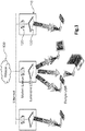
- the Fig. 1 schematically represents an example of a Li-Fi system.
- a plurality of light access points or APs, 110 are connected to the main network, 100, by means of Ethernet links.
- Each access point consists of a modem 120 coupled to an LED light source 130 emitting in the visible range, the modem modulating the power supply current of the source so as to modulate the intensity of the light emitted .
- the terminals are equipped with a dongle including an optical receiver. This optical receiver receives the light signal, converts it into an electrical signal, demodulates it and retrieves the transmitted data.
- the dongle (or the terminal itself) is also equipped with an infrared diode. The data at transmit on the upstream channel then modulate the infrared signal.
- the infrared signal is received by a photodiode (not shown) mounted on the access point, and is demodulated to transmit the data to the main network (Ethernet or other network).
- the modulation of optical signals on the uplink as on the downlink is a non-coherent modulation with a direct detection at the receiver.
- Different types of modulation have been proposed in the literature to take into account the real and unipolar nature of the light signal.
- OOK On Off Keying
- PAM Pulse Amplitude Modulation
- PPM Pulse Position Modulation
- DCO- OFDM Direct-Current Optical OFDM
- SIM-OFDM Subcarrier Index Modulation OFDM
- PAM modulation has been recommended on the uplink. Indeed, it has first of all the advantage of reducing the energy consumption of the terminal due to the absence of DC bias (unlike DCO-OFDM modulation in particular). Then, it allows to deport the channel equalization on the access point side. This equalization is generally performed in the frequency domain, which only requires the insertion of a cyclic prefix on the transmitter side. Thus, the computing resources of the terminal, which can be relatively constrained, are not solicited.
- a communication system with M-PAM modulation (MAP at M levels) on transmission and frequency domain equalization on reception was thus proposed in the article of MMA Mohammed et al. entitled "A spectrally efficient unipolar PAM single-carrier frequency domain equalization for IM / DD systems" published in 2015 IEEE Proc. of Photonics Conf. (IPC), Reston, VA, pp. 246-247 .
- the Fig. 2 schematically shows the structure of an M-PAM modulation transmitter for a wireless optical communication system.
- the data to be transmitted (binary words) are modulated by an M-PAM modulator (PAM with M levels), 210.
- the M-PAM symbols thus obtained are then filtered by means of a shaping filter 220 and then converted into a analog signal by a DAC 230.
- the purpose of formatting filtering is notably to reduce inter-channel interference adjacent.
- the analog signal is then amplified (in voltage or current) by an amplifier 240 before driving an LED source 250, for example an infrared LED source for the uplink and a white LED source (for example a blue LED with phosphor) for the downward path.
- LED source 250 for example an infrared LED source for the uplink and a white LED source (for example a blue LED with phosphor) for the downward path.
- DAC digital-to-analog converter
- the patent application CN-A-103986516 describes a transmitter of an optical communication system, making it possible to dispense with such a converter.
- the data to be transmitted is demultiplexed over a plurality of bit-channels, each bit-channel performing OOK modulation (equivalent to 2-PAM modulation) and switching a corresponding LED source into the visible range.
- OOK modulation equivalent to 2-PAM modulation
- the addition at the photodiode of the optical signals emitted in parallel by the different LED sources makes it possible to simulate an M-PAM modulation.
- M modulation levels
- the object of the present invention is therefore to provide a transmitter for optical communication system, in particular for the uplink of a Li-Fi system, which is particularly simple and robust, in particular in that it does not require a set of LED sources or a digital to analog converter.
- the conversion module is adapted to convert each M- PAM symbol into a binary word of size M -1, the intensities of the switched current sources having an identical value ( I 0 ).
- the conversion module is then adapted to convert each M- PAM symbol into a binary word comprising n bits in a first logic state and Nn bits in a complementary logic state, where n is the level of the M- PAM symbol.
- the binary word is a thermometric code word.
- m 0, ..., ⁇ -1 of the conversion module being chosen so that the light power of the optical source is equal to 2 m ⁇ 0 where ⁇ 0 is a predetermined luminous power.
- each of the branches is arranged in series between the optical source and the ground, each branch comprising a transistor and a resistor in series, the base of the transistor being connected to a corresponding logic output of the conversion module.
- each branch comprising a group of parallel transistors and a series resistor, the bases of said transistors of said group being connected to the same logic output of the conversion module.
- the optical communication system is for example a Li-Fi system.
- the optical source is typically an LED.
- the optical source used by the transmitter can be an LED source, a laser source, a vertical-Cavity Surface-Emitting Laser (VCSEL) or other type of laser diode.
- VCSEL vertical-Cavity Surface-Emitting Laser
- the optical source can be monochromatic or emit in a broad spectral band.
- the optical source may be an infrared LED.
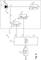
- the Fig. 3 schematically represents the structure of an M-PAM modulation transmitter for wireless optical communication system, according to a first embodiment of the invention.
- the transmitter 300 comprises an M-PAM modulator, 310, modulating the binary data into M-PAM symbols. More precisely, each binary word (of maximum size log 2 ( M )) is transformed by the modulator into an M-PAM symbol.
- the 8-PAM input symbols are denoted S 0 , ..., S 7 and the output word of the conversion module is denoted C 1 ,..., C 7. It will be noted that the bits of the output word presenting the first logical value (or the complementary logical value) are not necessarily contiguous as in the above example but may occupy arbitrary locations.
- the modulator M-PAM 310 and the conversion module 320 are advantageously produced by means of an FPGA programmable circuit or a dedicated integrated circuit of the ASIC type, or even by means of a digital signal processor DSP.
- the combination of the modulator M-PAM, 310, and the conversion module, 320 is performed by means of a binary transcoder with a thermometric, coding binary words of log 2 ( M ) bits in words. N bits.
- the alphabet of an N- bit thermometric code consists of M words, each word consisting of 0 ⁇ n ⁇ N LSB bits having a first logic value (for example "1"), the Nn bits of MSB having a complementary logical value.
- the binary word "101" is coded "0011111”.
- each logic output C 1 ,..., C N of the conversion module controls a switched current source, cs 1 , ..., cs N , of a module of the optical generator, 330.
- This optical generator comprises an optical source, for example an LED, 335 and a plurality N of parallel branches, 337, each of these branches being arranged in series with the optical source between a power source V cc and ground.
- Each branch 337 comprises a switched current source, 339, by a logic output of the conversion module 320.
- each branch comprises a transistor T operating in saturated-blocked mode, connected in series with a resistor R.
- the transistor may be a bipolar transistor or a MOS transistor.
- the characteristics of the transistors ( T ) and the values of the resistors ( R ) are chosen to be identical in the different branches.
- the current sources all generate an identical current I 0 and the emission current of the optical source (IR LED for example) can vary from 0 to NI 0 depending on the data to be transmitted.
- the characteristics of the transistors in the various branches are not strictly identical, it is advantageous to proceed to a phase of calibration of the resistances so that the currents generated by the switched current sources are nevertheless identical.
- Each switched current source can be made by paralleling a group of transistors, if the saturation current of a single transistor is insufficient.
- a logic output of the conversion module controls in parallel the bases of the transistors of said group.
- the optical transmitter requires only a single light source, the addition of the elementary intensities being carried out in the electrical domain and not in the optical domain.
- the Fig. 4 schematically represents the structure of an M-PAM modulation transmitter for wireless optical communication system, according to a second embodiment of the invention.
- This embodiment differs from the first in that the logic outputs of the conversion module are weighted and the currents in the different branches are also weighted.
- the optical transmitter comprises an M-PAM modulator, 410, and a conversion module 420.
- the modulator M-PAM 410 and the conversion module 420 are advantageously produced by means of an FPGA programmable circuit or a dedicated integrated circuit of the ASIC type, or even by means of a digital DSP signal processor.
- M 8: symbol 8-PAM C 1 C 2 C 3 S 0 0 0 0 S 1 1 0 0 S 2 0 1 0 S 3 1 1 0 S 4 0 0 1 S 5 1 0 1 S 6 0 1 1 S 7 1 1 1 1
- the combination of the modulator M-PAM and the conversion module can be achieved by a simple serial / parallel converter, 3 successive bits at the input of the modulator forming a word output of the conversion module.
- a simple serial / parallel converter 3 successive bits at the input of the modulator forming a word output of the conversion module.
- other conversion tables are possible by swapping the rows and / or columns of the table above.
- each logic output C 1 , ..., C ⁇ of the conversion module controls a switched current source, cs 1 ,..., Cs ⁇ , of a module of the optical generator, 430.
- the optical generator 430 comprises, as before, an optical source 435 (for example an LED) and a plurality of parallel branches, 437, each of these branches being arranged in series with the optical source between a supply source V cc and ground. Unlike the first embodiment however, the number of branches here is equal to ⁇ .
- a branch m comprises a current source 439, designated cs m , switched by C m , and intensity 2 m -1 I 0 .
- the switched current source can be realized by a transistor operating in saturated-blocked mode in series with a resistor R m .
- the values of the resistances R m are determined, if necessary during a calibration phase, so that the currents generated by cs 1 , ..., cs ⁇ are equal to I 0 , 2 I 0 , ..., 2 ⁇ - 1 I 0 .
- the emission current sources of the optical source can vary from 0 to NI 0 depending on the data to be transmitted.
- the currents of the switched current sources are chosen so that the light intensity of the optical source takes the values ⁇ 0 , 2 I 0 , ..., 2 ⁇ -1 ⁇ 0 (where ⁇ 0 is a predetermined luminous power), when the current sources cs 1 , ..., cs ⁇ are respectively activated.
- the transmitter according to the first or the second embodiment can also implement a second modulation in addition to the M-PAM modulation.
- the logic outputs controlling the commutation of the current sources are also modulated in pulse position or PPM (Pulse Position Modulation) to provide an additional degree of modulation or in pulse width or PWM (Pulse Width Modulation) so that the lighting level can be dimmed.
- PPM Pulse Position Modulation
- PWM Pulse Width Modulation
Landscapes
- Physics & Mathematics (AREA)
- Electromagnetism (AREA)
- Engineering & Computer Science (AREA)
- Computer Networks & Wireless Communication (AREA)
- Signal Processing (AREA)
- Optical Communication System (AREA)
Abstract
Description
- La présente invention concerne de manière générale le domaine des communications optiques sans-fil et plus particulièrement celui des systèmes de communication Li-Fi (Light Fidelity).
- Les systèmes de communications optiques sans fil ou OWC (Optical Wireless Communications) ont fait dernièrement l'objet d'importantes recherches en raison de leur capacité à résoudre le problème d'occupation spectrale et à compléter voire à se substituer aux systèmes Wi-Fi.
- De manière schématique, les systèmes Li-Fi sont analogues aux systèmes Wi-Fi (obéissant à la norme IEEE 802.11) mais utilisent le spectre visible au lieu du spectre RF. La couche physique (PHY) et la couche MAC des systèmes Li-Fi ont déjà fait l'objet d'une normalisation dans le standard IEEE 802.15.7.
- La
Fig. 1 représente de manière schématique un exemple de système Li-Fi. - Une pluralité de points d'accès lumineux ou APs, 110, sont connectés au réseau principal, 100, au moyen de liaisons Ethernet. Chaque point d'accès est constitué d'un modem 120 couplé à une source lumineuse à LED, 130, émettant dans le domaine visible, le modem modulant le courant d'alimentation de la source de manière à moduler l'intensité de la lumière émise. Les terminaux sont équipés d'un dongle incluant un récepteur optique. Ce récepteur optique reçoit le signal lumineux, le convertit en signal électrique, le démodule et récupère les données émises. Inversement, le dongle (ou le terminal lui-même) est également équipé d'une diode infrarouge. Les données à transmettre sur la voie montante modulent alors le signal infrarouge. Le signal infrarouge est reçu par une photodiode (non représentée) montée sur le point d'accès, puis est démodulé pour transmettre les données vers le réseau principal (réseau Ethernet ou autre).
- La modulation des signaux optiques sur la voie montante comme sur la voie descendante est une modulation non-cohérente avec une détection directe au niveau du récepteur. Différents types de modulation ont été proposés dans la littérature pour tenir compte de la nature réelle et unipolaire du signal lumineux. Ainsi, les modulations OOK (On Off Keying), PAM (Pulse Amplitude Modulation), PPM (Pulse Position Modulation), DCO-OFDM (Direct-Current Optical OFDM), SIM-OFDM (Subcarrier Index Modulation OFDM) ont été envisagées.
- La modulation PAM a notamment été préconisée sur la voie montante. En effet, elle présente tout d'abord l'avantage de réduire la consommation énergétique du terminal en raison de l'absence de polarisation DC (contrairement notamment à la modulation DCO-OFDM). Ensuite, elle permet de déporter l'égalisation de canal du côté du point d'accès. Cette égalisation est généralement réalisée dans le domaine fréquentiel, ce qui ne nécessite que l'insertion d'un préfixe cyclique du côté de l'émetteur. Ainsi, les ressources de calcul du terminal, qui peuvent être relativement contraintes, ne sont pas sollicitées. Un système de communication avec modulation M-PAM (PAM à M niveaux) à l'émission et égalisation dans le domaine fréquentiel à la réception été ainsi proposé dans l'article de M.M.A. Mohammed et al. intitulé « A spectrally efficient unipolar PAM single-carrier frequency domain equalization for IM/DD systems » publié dans 2015 IEEE Proc. of Photonics Conf. (IPC), Reston, VA, pp. 246-247.
- La
Fig. 2 représente de manière schématique la structure d'un émetteur à modulation M-PAM pour un système de communication optique sans fil. - Les données à émettre (mots binaires) sont modulées par un modulateur M-PAM (PAM à M niveaux), 210. Les symboles M-PAM ainsi obtenus sont ensuite filtrés au moyen d'un filtre de mise en forme 220 puis convertis en un signal analogique par un DAC 230. Le filtrage de mise en forme a notamment pour objet de réduire l'interférence entre canaux adjacents. Le signal analogique est ensuite amplifié (en tension ou en courant) par un amplificateur 240 avant de piloter une source LED 250, par exemple une source LED infrarouge pour la voie montante et une source LED blanche (par exemple une LED bleue avec luminophore) pour la voie descendante.
- L'émetteur de la
Fig. 2 présente toutefois l'inconvénient de nécessiter un convertisseur numérique/ analogique (DAC). - La demande de brevet
CN-A-103986516 décrit un émetteur d'un système de communication optique, permettant de se passer d'un tel convertisseur. Les données à transmettre sont démultiplexées sur une pluralité de voies binaires, chaque voie binaire effectuant une modulation OOK (équivalente à modulation 2-PAM) et commutant une source LED correspondante dans le domaine visible. L'addition au niveau de la photodiode des signaux optiques émis en parallèle par les différentes sources LED permet de simuler une modulation M-PAM. Toutefois, cette configuration présente l'inconvénient de nécessiter autant de sources LED que de niveaux de modulation (M) et de synchroniser l'émission de ces différentes sources. En outre, elle ne fonctionne pas de manière satisfaisante lorsque les caractéristiques des canaux entre les différentes sources LED et la photodiode du récepteur ne sont pas identiques. - Le but de la présente invention est par conséquent de proposer un émetteur pour système de communication optique, en particulier pour la voie montante d'un système Li-Fi, qui soit particulièrement simple et robuste, notamment en ce qu'il ne nécessite ni un ensemble de sources LED ni un convertisseur numérique analogique.
- La présente invention est définie par un émetteur pour système de communication optique sans fil comprenant un modulateur M -PAM transformant des données à transmettre en des symboles d'alphabet PAM à M niveaux où M > 2 et une source optique destinée à transmettre lesdites données, ledit émetteur comprenant :
- un module de conversion adapté à convertir, à partir d'une table de conversion biunivoque, chaque symbole M -PAM en une pluralité de sorties logiques ;
- une pluralité de branches en parallèle, chaque branche comprenant une source de courant commutée, montée en série avec la source optique, chaque source de courant commutée étant contrôlée par une sortie logique du module de conversion.
- Selon un premier mode de réalisation, le module de conversion est adapté à convertir chaque symbole M -PAM en un mot binaire de taille M -1, les intensités des sources de courant commutées ayant une valeur identique (I 0).
- Le module de conversion est alors adapté à convertir chaque symbole M -PAM en un mot binaire comprenant n bits dans un premier état logique et N-n bits dans un état logique complémentaire, n étant le niveau du symbole M -PAM.
- Avantageusement, le mot binaire est un mot de code thermométrique.
- Selon un second mode de réalisation, le module de conversion est adapté à convertir chaque symbole M -PAM en un mot binaire de taille µ = log2(M), les intensités des sources de courant commutées ayant des valeurs égales à I 0,2I 0,...,2 µ-1 I 0 où I 0 est une valeur d'intensité prédéterminée.
- Selon une variante du second mode de réalisation, le module de conversion est adapté à convertir chaque symbole M -PAM en un mot binaire de taille µ=log2(M), l'intensité de la source de courant commutée connectée à la sortie logique m=0,...,µ-1 du module de conversion étant choisie de manière à ce que la puissance lumineuse de la source optique soit égale à 2 m Φ0 où Φ0 est une puissance lumineuse prédéterminée.
- Selon une première configuration, chacune des branches est disposée en série entre la source optique et la masse, chaque branche comprenant un transistor et une résistance en série, la base du transistor étant connectée à une sortie logique correspondante du module de conversion.
- Selon une seconde configuration, chaque branche comprenant un groupe de transistors en parallèle et une résistance en série, les bases desdits transistors dudit groupe étant connectées à une même sortie logique du module de conversion.
- Le système de communication optique est par exemple un système Li-Fi. La source optique est typiquement une LED.
- D'autres caractéristiques et avantages de l'invention apparaîtront à la lecture d'un mode de réalisation préférentiel de l'invention, fait en référence aux figures jointes parmi lesquelles :
- La
Fig. 1 , déjà décrite, représente schématiquement un exemple de système Li-Fi, connu de l'état de la technique ; - La
Fig. 2 , déjà décrite, représente schématiquement un émetteur à modulation M-PAM pour un système de communication optique sans fil connu de l'état de la technique ; - La
Fig. 3 représente schématiquement la structure d'un émetteur à modulation M-PAM pour système de communication optique sans fil, selon un premier mode de réalisation de l'invention ; - La
Fig. 4 représente schématiquement la structure d'un émetteur à modulation M-PAM pour système de communication optique sans fil, selon un second mode de réalisation de l'invention. - On considérera dans la suite un émetteur pour un système de communication optique sans fil, par exemple un système de communication Li-Fi. La source optique utilisée par l'émetteur peut être une source LED, une source laser, une diode laser de type VCSEL (Vertical-Cavity Surface-Emitting Laser) ou autre. Aucune hypothèse n'est faite ici sur le spectre d'émission : la source optique peut être monochromatique ou émettre dans une large bande spectrale. En particulier, si l'émetteur est utilisé pour la voie montante d'un système Li-Fi, la source optique pourra être une LED infrarouge.
- La
Fig. 3 représente schématiquement la structure d'un émetteur à modulation M-PAM pour système de communication optique sans fil, selon un premier mode de réalisation de l'invention. - L'émetteur 300 comprend un modulateur M-PAM, 310, modulant les données binaires en symboles M-PAM. Plus précisément, chaque mot binaire (de taille maximale log2(M)) est transformé par le modulateur en un symbole M-PAM. Les symboles M-PAM sont ensuite fournis à un module de conversion, 320, faisant correspondre à un symbole de modulation M-PAM, Sn , 0≤n≤N, avec N=M-1 (où M est la taille de l'alphabet PAM) un mot binaire de N bits comprenant n bits dans un premier état logique et N-n bits dans un état logique complémentaire.
- On trouvera ci-après un exemple de table de conversion pour le cas M=8 (N=7) :
Symbole 8-PAM C1 C2 C3 C4 C5 C6 C7 S0 0 0 0 0 0 0 0 S1 1 0 0 0 0 0 0 S2 1 1 0 0 0 0 0 S3 1 1 1 0 0 0 0 S4 1 1 1 1 0 0 0 S5 1 1 1 1 1 0 0 S6 1 1 1 1 1 1 0 S7 1 1 1 1 1 1 1 - Les symboles 8-PAM en entrée sont notés S 0,...,S 7 et le mot en sortie du module de conversion est noté C 1,...,C 7, On notera que les bits du mot de sortie présentant la première valeur logique (ou la valeur logique complémentaire) ne sont pas nécessairement contigus comme dans l'exemple ci-dessus mais peuvent occuper des emplacements arbitraires.
- Le modulateur M-PAM, 310, et le module de conversion, 320, sont avantageusement réalisés au moyen d'un circuit programmable FPGA ou d'un circuit intégré dédié de type ASIC, voire au moyen d'un processeur numérique de signal DSP.
- Selon un mode particulier de réalisation, la combinaison du modulateur M-PAM, 310, et du module de conversion, 320, est réalisée au moyen d'un transcodeur binaire à thermométrique, codant des mots binaires de log2(M) bits en mots de N bits. On rappelle que l'alphabet d'un code thermométrique sur N bits est constitué de M mots, chaque mot étant constitué de 0≤n≤N bits de LSB ayant une première valeur logique (par exemple « 1 »), les N-n bits de MSB ayant une valeur logique complémentaire. Ainsi, par exemple, pour M=8, le mot binaire « 101 » est codé « 0011111 ».
- Quel que soit le mode de réalisation envisagé, chaque sortie logique C 1 ,...,CN du module de conversion commande une source de courant commutée, cs 1,...,csN , d'un module du générateur optique, 330. Ce générateur optique comprend une source optique, par exemple une LED, 335 et une pluralité N de branches parallèles, 337, chacune de ces branches étant disposée en série avec la source optique entre une source d'alimentation Vcc et la masse. Chaque branche 337 comprend une source de courant commutée, 339, par une sortie logique du module de conversion 320. Par exemple, chaque branche comprend un transistor T fonctionnant en mode saturé-bloqué, monté en série avec une résistance R. Le transistor peut être un transistor bipolaire ou un transistor MOS. Les caractéristiques des transistors (T) et les valeurs des résistances (R) sont choisies identiques dans les différentes branches. Ainsi, les sources de courant génèrent toutes un courant identique I 0 et le courant d'émission de la source optique (LED IR par exemple) peut varier de 0 à NI 0 en fonction de la donnée à émettre. Toutefois, si les caractéristiques des transistors dans les différentes branches ne sont pas rigoureusement identiques, on pourra avantageusement procéder à une phase de calibration des résistances pour que les courants générés par les sources de courant commutées soient néanmoins identiques.
- Chaque source de courant commutée peut être réalisée par la mise en parallèle d'un groupe de transistors, si le courant de saturation d'un seul transistor s'avère insuffisant. Dans ce cas, une sortie logique du module de conversion contrôle en parallèle les bases des transistors dudit groupe.
- On remarquera que contrairement à l'art antérieur, l'émetteur optique ne nécessite qu'une seule source lumineuse, l'addition des intensités élémentaires étant réalisée dans le domaine électrique et non dans le domaine optique.
- La
Fig. 4 représente schématiquement la structure d'un émetteur à modulation M-PAM pour système de communication optique sans fil, selon un second mode de réalisation de l'invention. - Ce mode de réalisation diffère du premier en ce que les sorties logiques du module de conversion sont pondérées et que les courants dans les différentes branches le sont également.
- Plus précisément, l'émetteur optique comprend un modulateur M-PAM, 410, et un module de conversion 420. Le module de conversion, 420, faisant correspondre à chaque symbole de modulation M-PAM, Sn , 0≤n≤N, avec N=M-1 un mot binaire de µ=log2(M) bits.
- Comme dans le premier mode de réalisation, le modulateur M-PAM, 410, et le module de conversion, 420, sont avantageusement réalisés au moyen d'un circuit programmable FPGA ou d'un circuit intégré dédié de type ASIC, voire au moyen d'un processeur numérique de signal DSP.
- Selon un exemple, le module de conversion peut utiliser une table de conversion particulièrement simple, dans laquelle on fait correspondre à chaque symbole Sn , le niveau de modulation n exprimé en binaire, sur µ=log2(M) bits, C 1,...,Cµ . Ainsi, pour le cas M=8 :
symbole 8-PAM C1 C2 C3 S0 0 0 0 S1 1 0 0 S2 0 1 0 S3 1 1 0 S4 0 0 1 S5 1 0 1 S6 0 1 1 S7 1 1 1 - Dans cet exemple de réalisation particulièrement simple, la combinaison du modulateur M-PAM et du module de conversion peut être réalisée par un simple convertisseur série/parallèle, 3 bits successifs en entrée du modulateur formant un mot en sortie du module de conversion. Bien entendu, toutefois, d'autres tables de conversion sont possibles en permutant les lignes et/ou les colonnes de la table ci-dessus.
- Quel que soit la table de conversion envisagée, chaque sortie logique C 1,...,Cµ du module de conversion commande une source de courant commutée, cs 1,...,csµ, d'un module du générateur optique, 430. A la différence du premier mode de réalisation, les sources de courant commutées sont d'intensités différentes, la source de courant commutée csm, m=1,..,µ générant un courant d'intensité 2 m-1 I 0 où I 0 est le courant générée par la source de courant cs 1, associé au LSB du mot en sortie du module de conversion.
- Le générateur optique 430 comprend comme précédemment une source optique 435 (par exemple une LED) et une pluralité de branches parallèles, 437, chacune de ces branches étant disposée en série avec la source optique entre une source d'alimentation Vcc et la masse. A la différence du premier mode de réalisation toutefois, le nombre de branches est ici égal à µ. Une branche m comprend une source de courant 439, désignée par csm, commutée par Cm, et d'intensité 2 m-1 I 0. La source de courant commutée peut être réalisée par un transistor opérant en mode saturé-bloqué en série avec une résistance Rm . Les valeurs des résistances Rm sont déterminées, le cas échéant lors d'une phase de calibration, de sorte que les courants générés par cs 1,...,csµ soient égaux à I 0,2I 0,...,2 µ-1 I 0. Ainsi, les sources de courant d'émission de la source optique (LED IR par exemple) peut varier de 0 à NI 0 en fonction de la donnée à émettre.
- Alternativement, selon une variante du second mode de réalisation, pour tenir compte des non-linéarités éventuelles de la source optique, les courants des sources de courant commutées sont choisies de manière à ce que l'intensité lumineuse de la source optique prenne les valeurs Φ0,2I 0,...,2 µ-1Φ0 (où Φ0 est une puissance lumineuse prédéterminée), lorsque les sources de courant cs 1,...,csµ sont respectivement activées. Pour ce faire, les résistances sont réglées en conséquence dans une phase de calibration, la résistance Rm, m=0,...,µ-1 étant choisie telle que l'intensité lumineuse de la source optique soit égale à 2 m Φ0 lorsque la source de courant csm est activée et que les autres sources de courant sont coupées.
- Il est important de noter que l'émetteur selon le premier ou le second mode de réalisation peut également mettre en oeuvre une seconde modulation en sus de la modulation M-PAM. Par exemple, on pourra prévoir que les sorties logiques commandant la commutation des sources de courant sont également modulées en position d'impulsion ou PPM (Pulse Position Modulation) pour offrir un degré de modulation supplémentaire ou bien en largeur d'impulsion ou PWM (Pulse Width Modulation) de manière à pouvoir effectuer une gradation du niveau d'éclairage.
- En outre, dans le premier mode de réalisation comme dans le second mode de réalisation, on pourra ne pas utiliser le mot de commande C 1=C 2=...CN =0 (correspondant à une intensité de courant nulle) pour coder un symbole PAM, ce afin de distinguer le symbole en question d'une absence de transmission, due à une panne par exemple.
Claims (10)
- Emetteur pour système de communication optique sans fil comprenant un modulateur M-PAM (310,410) transformant des données à transmettre en des symboles d'alphabet PAM à M niveaux où M>2 et une source optique (335,435) destinée à transmettre lesdites données, caractérisé en ce qu'il comprend :- un module de conversion (320,420) adapté à convertir, à partir d'une table de conversion biunivoque, chaque symbole M -PAM en une pluralité de sorties logiques ;- une pluralité de branches en parallèle (337,437), chaque branche comprenant une source de courant commutée (339, 439), montée en série avec la source optique, chaque source de courant commutée étant contrôlée par une sortie logique du module de conversion.
- Emetteur selon la revendication 1, caractérisé en ce que le module de conversion est adapté à convertir chaque symbole M -PAM en un mot binaire de taille M-1, les intensités des sources de courant commutées ayant une valeur identique (I 0).
- Emetteur selon la revendication 2, caractérisé en ce que le module de conversion est adapté à convertir chaque symbole M -PAM en un mot binaire comprenant n bits dans un premier état logique et N-n bits dans un état logique complémentaire, n étant le niveau du symbole M -PAM.
- Emetteur selon la revendication 3, caractérisé en ce que le mot binaire est un mot de code thermométrique.
- Emetteur selon la revendication 1, caractérisé en ce que le module de conversion est adapté à convertir chaque symbole M -PAM en un mot binaire de taille µ=log2(M), les intensités des sources de courant commutées ayant des valeurs égales à I 0,2I 0,...,2 µ-1 I 0 où I 0 est une valeur d'intensité prédéterminée.
- Emetteur selon la revendication 1, caractérisé en ce que le module de conversion est adapté à convertir chaque symbole M -PAM en un mot binaire de taille µ=log2(M), l'intensité de la source de courant commutée connectée à la sortie logique m=0,...,µ-1 du module de conversion étant choisie de manière à ce que la puissance lumineuse de la source optique soit égale à 2 m Φ0 où Φ0 est une puissance lumineuse prédéterminée.
- Emetteur selon l'une des revendications précédentes, caractérisé en ce que chacune des branches est disposée en série entre la source optique et la masse, chaque branche comprenant un transistor et une résistance en série, la base du transistor étant connectée à une sortie logique correspondante du module de conversion.
- Emetteur selon l'une des revendications 1 à 6, caractérisé en ce que chacune des branches est disposée en série entre la source optique et la masse, chaque branche comprenant un groupe de transistors en parallèle et une résistance en série, les bases desdits transistors dudit groupe étant connectées à une même sortie logique du module de conversion.
- Emetteur selon l'une des revendications précédentes, caractérisé en ce que le système de communication optique est un système Li-Fi.
- Emetteur selon l'une des revendications précédentes, caractérisé en ce que la source optique est une LED.
Applications Claiming Priority (1)
| Application Number | Priority Date | Filing Date | Title |
|---|---|---|---|
| FR1755219A FR3067532B1 (fr) | 2017-06-12 | 2017-06-12 | Emetteur a modulation m-pam pour systeme de communication optique sans fil |
Publications (2)
| Publication Number | Publication Date |
|---|---|
| EP3416306A1 true EP3416306A1 (fr) | 2018-12-19 |
| EP3416306B1 EP3416306B1 (fr) | 2020-12-16 |
Family
ID=59811494
Family Applications (1)
| Application Number | Title | Priority Date | Filing Date |
|---|---|---|---|
| EP18177325.0A Active EP3416306B1 (fr) | 2017-06-12 | 2018-06-12 | Émetteur à modulation m-pam pour système de communication optique sans fil |
Country Status (3)
| Country | Link |
|---|---|
| US (1) | US10498455B2 (fr) |
| EP (1) | EP3416306B1 (fr) |
| FR (1) | FR3067532B1 (fr) |
Families Citing this family (3)
| Publication number | Priority date | Publication date | Assignee | Title |
|---|---|---|---|---|
| US20240235676A1 (en) * | 2021-04-30 | 2024-07-11 | Hewlett-Packard Development Company, L.P. | Electronic devices employing optical communications |
| CN116405353A (zh) * | 2023-04-21 | 2023-07-07 | 山东云海国创云计算装备产业创新中心有限公司 | 基于无线通信系统的调制解调方法、系统、介质及设备 |
| CN119182463B (zh) * | 2024-08-29 | 2025-10-24 | 武汉邮电科学研究院有限公司 | 双重加密的时域混合pam编码方法、解码方法及系统 |
Citations (3)
| Publication number | Priority date | Publication date | Assignee | Title |
|---|---|---|---|---|
| CN103986516A (zh) * | 2014-05-30 | 2014-08-13 | 中国人民解放军信息工程大学 | 一种可见光通信系统及方法 |
| US20160156417A1 (en) * | 2014-11-28 | 2016-06-02 | Sumitomo Electric Industries, Ltd. | Driver for Pulse Amplitude Modulation and Optical Transmitter Implementing the Same |
| US20160164604A1 (en) * | 2013-07-31 | 2016-06-09 | Kuang-Chi Innovative Technology Ltd. | Multi-stage amplitude modulation-based methods, apparatuses and systems for coding and decoding visible light signal |
Family Cites Families (24)
| Publication number | Priority date | Publication date | Assignee | Title |
|---|---|---|---|---|
| DE60138089D1 (de) * | 2000-01-17 | 2009-05-07 | Broadcom Corp | Hochgeschwindigkeitsübertragungssystem für optische kanäle |
| US6424444B1 (en) * | 2001-01-29 | 2002-07-23 | Stratalight Communications, Inc. | Transmission and reception of duobinary multilevel pulse-amplitude-modulated optical signals using finite-state machine-based encoder |
| US6643471B2 (en) * | 2001-04-02 | 2003-11-04 | Adc Telecommunications, Inc. | Increased transmission capacity for a fiber-optic link |
| US20040091270A1 (en) * | 2001-08-01 | 2004-05-13 | Youngwan Choi | Optical transmitter receiver for free space optical communication and network system and application apparatus thereof |
| EP1696586A1 (fr) * | 2005-02-28 | 2006-08-30 | Sony Deutschland GmbH | Procédé de transmission optique sans fil et système de transmission optique sans fils de données. |
| US7613400B2 (en) * | 2006-06-30 | 2009-11-03 | Intel Corporation | Multi-level optical data communication circuit |
| US8634725B2 (en) * | 2010-10-07 | 2014-01-21 | Electronics And Telecommunications Research Institute | Method and apparatus for transmitting data using visible light communication |
| CA2823152C (fr) * | 2010-12-26 | 2019-08-06 | The Travelers Indemnity Company | Systemes et procedes d'utilisation de zones a risques |
| US8452189B2 (en) * | 2011-01-19 | 2013-05-28 | Avago Technologies General Ip (Singapore) Pte. Ltd. | Source-multiplexed pulse amplitude modulation (PAM) optical data communication system and method |
| DE102012001398B4 (de) * | 2012-01-26 | 2015-09-24 | Airbus Defence and Space GmbH | Sendevorrichtung zur optischen Freiraum-Datenkommunikation basierend auf diskreten Leistungspegeln nebst Verwendung |
| US9306780B2 (en) * | 2013-03-11 | 2016-04-05 | Semtech Corporation | Optical transmission for binary and duobinary modulation formats |
| US9094130B2 (en) * | 2013-04-24 | 2015-07-28 | Broadcom Corporation | Linearization of optical intensity modulation systems |
| US8989300B1 (en) * | 2013-09-06 | 2015-03-24 | Avago Technologies General Ip (Singapore) Pte. Ltd. | Multi-level coding and distortion compensation |
| JP6413265B2 (ja) * | 2014-03-12 | 2018-10-31 | 住友電気工業株式会社 | 光変調器駆動回路 |
| US9733542B2 (en) * | 2014-08-25 | 2017-08-15 | Futurewei Technologies, Inc. | Multi-segment Mach-Zehnder modulator-driver system |
| JP2017028043A (ja) * | 2015-07-21 | 2017-02-02 | 住友電気工業株式会社 | レーザ駆動回路 |
| US9882532B1 (en) * | 2016-03-04 | 2018-01-30 | Inphi Corporation | Linear amplifier with extended linear output range |
| US10084619B2 (en) * | 2016-06-03 | 2018-09-25 | International Business Machines Corporation | Nested feed-forward optical equalization using an electro-optic modulator with a multi-segment electrode |
| US10587255B2 (en) * | 2016-07-22 | 2020-03-10 | Skorpios Technologies, Inc. | Multi-level output driver with adjustable pre-distortion capability |
| EP3280074B1 (fr) * | 2016-08-01 | 2018-11-14 | Knowledge Development for POF SL | Pilote de del pour communications optiques à grande vitesse sur la base de modulations linéaires |
| US9933639B1 (en) * | 2016-11-08 | 2018-04-03 | Xilinx, Inc. | Electro-absorption modulation with an integrated photodetector |
| JP6907734B2 (ja) * | 2017-06-09 | 2021-07-21 | 住友電気工業株式会社 | 駆動回路 |
| JP2019012898A (ja) * | 2017-06-29 | 2019-01-24 | ルネサスエレクトロニクス株式会社 | 光駆動装置および光通信システム |
| JP6998691B2 (ja) * | 2017-07-19 | 2022-01-18 | 日本ルメンタム株式会社 | 光送信モジュール |
-
2017
- 2017-06-12 FR FR1755219A patent/FR3067532B1/fr not_active Expired - Fee Related
-
2018
- 2018-06-12 EP EP18177325.0A patent/EP3416306B1/fr active Active
- 2018-06-12 US US16/006,190 patent/US10498455B2/en active Active
Patent Citations (3)
| Publication number | Priority date | Publication date | Assignee | Title |
|---|---|---|---|---|
| US20160164604A1 (en) * | 2013-07-31 | 2016-06-09 | Kuang-Chi Innovative Technology Ltd. | Multi-stage amplitude modulation-based methods, apparatuses and systems for coding and decoding visible light signal |
| CN103986516A (zh) * | 2014-05-30 | 2014-08-13 | 中国人民解放军信息工程大学 | 一种可见光通信系统及方法 |
| US20160156417A1 (en) * | 2014-11-28 | 2016-06-02 | Sumitomo Electric Industries, Ltd. | Driver for Pulse Amplitude Modulation and Optical Transmitter Implementing the Same |
Also Published As
| Publication number | Publication date |
|---|---|
| US10498455B2 (en) | 2019-12-03 |
| US20180359034A1 (en) | 2018-12-13 |
| FR3067532B1 (fr) | 2019-06-21 |
| EP3416306B1 (fr) | 2020-12-16 |
| FR3067532A1 (fr) | 2018-12-14 |
Similar Documents
| Publication | Publication Date | Title |
|---|---|---|
| Chun et al. | LED based wavelength division multiplexed 10 Gb/s visible light communications | |
| US8208818B2 (en) | Optical free space transmission system using visible light and infrared light | |
| Islim et al. | Modulation techniques for li-fi | |
| FR2888431A1 (fr) | Systeme de communication optique,dispositif d'illumination et dispositif de terminal utilises dans celui-ci. | |
| Popoola et al. | Demonstration of the merit and limitation of generalised space shift keying for indoor visible light communications | |
| KR101408816B1 (ko) | 가시광 통신용 송신기 및 가시광 통신 시스템 | |
| EP3416306B1 (fr) | Émetteur à modulation m-pam pour système de communication optique sans fil | |
| EP2478650B1 (fr) | Appareil et procédé destinés à produire des trames à haute résolution pour un support de visibilité et de gradation dans un système de communication par lumière visible | |
| Bian et al. | 10.2 Gb/s visible light communication with off-the-shelf LEDs | |
| US10263710B2 (en) | Electronic device associated with a photovoltaic module to optimise the throughput of a bidirectional VLC transmission | |
| JP6994598B2 (ja) | 光データ伝送システム及び方法 | |
| WO2007101942A1 (fr) | Dispositif d’emission electroluminescent pour la transmission optique en espace libre | |
| Griffiths et al. | CMOS-integrated GaN LED array for discrete power level stepping in visible light communications | |
| EP3474470A1 (fr) | Mise en forme de signal probabiliste et correction d'erreur sans voie de retour par multiplexage de sous-porteuse | |
| FR2534746A1 (fr) | Emetteur laser et procede pour le faire fonctionner | |
| Thai | Real-time 138-kb/s transmission using OLED with 7-kHz modulation bandwidth | |
| Li et al. | Adaptive visible light communication LED receiver | |
| US10411799B1 (en) | Optical wireless communication systems with hadamard coded modulation | |
| EP3482493B1 (fr) | Systeme de suivi de la puissance crete d'un signal de telecommunication et procede de calcul de valeur de crete et de selection de tension d'alimentation associe | |
| EP3984135B1 (fr) | Émetteur uwb compact à très basse consommation et forme d'onde reconfigurable | |
| US20040126113A1 (en) | Using active and passive optical components | |
| FR3019268A1 (fr) | Dispositif de commande de l'intensite lumineuse d'ambiance d'un systeme d'eclairage et de transfert de donnees | |
| WO2024200289A1 (fr) | Système de communication optique sans fil | |
| Khan | Energy Efficient Optical Wireless Communications based on Frequency-Shift Keying Modulations. | |
| FR3127092A1 (fr) | Système et procédé de communication par voie lumineuse |
Legal Events
| Date | Code | Title | Description |
|---|---|---|---|
| PUAI | Public reference made under article 153(3) epc to a published international application that has entered the european phase |
Free format text: ORIGINAL CODE: 0009012 |
|
| STAA | Information on the status of an ep patent application or granted ep patent |
Free format text: STATUS: REQUEST FOR EXAMINATION WAS MADE |
|
| 17P | Request for examination filed |
Effective date: 20180612 |
|
| AK | Designated contracting states |
Kind code of ref document: A1 Designated state(s): AL AT BE BG CH CY CZ DE DK EE ES FI FR GB GR HR HU IE IS IT LI LT LU LV MC MK MT NL NO PL PT RO RS SE SI SK SM TR |
|
| AX | Request for extension of the european patent |
Extension state: BA ME |
|
| GRAP | Despatch of communication of intention to grant a patent |
Free format text: ORIGINAL CODE: EPIDOSNIGR1 |
|
| STAA | Information on the status of an ep patent application or granted ep patent |
Free format text: STATUS: GRANT OF PATENT IS INTENDED |
|
| INTG | Intention to grant announced |
Effective date: 20200731 |
|
| GRAS | Grant fee paid |
Free format text: ORIGINAL CODE: EPIDOSNIGR3 |
|
| GRAA | (expected) grant |
Free format text: ORIGINAL CODE: 0009210 |
|
| STAA | Information on the status of an ep patent application or granted ep patent |
Free format text: STATUS: THE PATENT HAS BEEN GRANTED |
|
| AK | Designated contracting states |
Kind code of ref document: B1 Designated state(s): AL AT BE BG CH CY CZ DE DK EE ES FI FR GB GR HR HU IE IS IT LI LT LU LV MC MK MT NL NO PL PT RO RS SE SI SK SM TR |
|
| REG | Reference to a national code |
Ref country code: GB Ref legal event code: FG4D Free format text: NOT ENGLISH |
|
| REG | Reference to a national code |
Ref country code: IE Ref legal event code: FG4D Free format text: LANGUAGE OF EP DOCUMENT: FRENCH |
|
| REG | Reference to a national code |
Ref country code: DE Ref legal event code: R096 Ref document number: 602018010775 Country of ref document: DE |
|
| REG | Reference to a national code |
Ref country code: AT Ref legal event code: REF Ref document number: 1346553 Country of ref document: AT Kind code of ref document: T Effective date: 20210115 |
|
| PG25 | Lapsed in a contracting state [announced via postgrant information from national office to epo] |
Ref country code: GR Free format text: LAPSE BECAUSE OF FAILURE TO SUBMIT A TRANSLATION OF THE DESCRIPTION OR TO PAY THE FEE WITHIN THE PRESCRIBED TIME-LIMIT Effective date: 20210317 Ref country code: NO Free format text: LAPSE BECAUSE OF FAILURE TO SUBMIT A TRANSLATION OF THE DESCRIPTION OR TO PAY THE FEE WITHIN THE PRESCRIBED TIME-LIMIT Effective date: 20210316 Ref country code: FI Free format text: LAPSE BECAUSE OF FAILURE TO SUBMIT A TRANSLATION OF THE DESCRIPTION OR TO PAY THE FEE WITHIN THE PRESCRIBED TIME-LIMIT Effective date: 20201216 Ref country code: RS Free format text: LAPSE BECAUSE OF FAILURE TO SUBMIT A TRANSLATION OF THE DESCRIPTION OR TO PAY THE FEE WITHIN THE PRESCRIBED TIME-LIMIT Effective date: 20201216 |
|
| REG | Reference to a national code |
Ref country code: AT Ref legal event code: MK05 Ref document number: 1346553 Country of ref document: AT Kind code of ref document: T Effective date: 20201216 |
|
| REG | Reference to a national code |
Ref country code: NL Ref legal event code: MP Effective date: 20201216 |
|
| PG25 | Lapsed in a contracting state [announced via postgrant information from national office to epo] |
Ref country code: SE Free format text: LAPSE BECAUSE OF FAILURE TO SUBMIT A TRANSLATION OF THE DESCRIPTION OR TO PAY THE FEE WITHIN THE PRESCRIBED TIME-LIMIT Effective date: 20201216 Ref country code: LV Free format text: LAPSE BECAUSE OF FAILURE TO SUBMIT A TRANSLATION OF THE DESCRIPTION OR TO PAY THE FEE WITHIN THE PRESCRIBED TIME-LIMIT Effective date: 20201216 Ref country code: BG Free format text: LAPSE BECAUSE OF FAILURE TO SUBMIT A TRANSLATION OF THE DESCRIPTION OR TO PAY THE FEE WITHIN THE PRESCRIBED TIME-LIMIT Effective date: 20210316 |
|
| PG25 | Lapsed in a contracting state [announced via postgrant information from national office to epo] |
Ref country code: HR Free format text: LAPSE BECAUSE OF FAILURE TO SUBMIT A TRANSLATION OF THE DESCRIPTION OR TO PAY THE FEE WITHIN THE PRESCRIBED TIME-LIMIT Effective date: 20201216 Ref country code: NL Free format text: LAPSE BECAUSE OF FAILURE TO SUBMIT A TRANSLATION OF THE DESCRIPTION OR TO PAY THE FEE WITHIN THE PRESCRIBED TIME-LIMIT Effective date: 20201216 |
|
| REG | Reference to a national code |
Ref country code: LT Ref legal event code: MG9D |
|
| PG25 | Lapsed in a contracting state [announced via postgrant information from national office to epo] |
Ref country code: LT Free format text: LAPSE BECAUSE OF FAILURE TO SUBMIT A TRANSLATION OF THE DESCRIPTION OR TO PAY THE FEE WITHIN THE PRESCRIBED TIME-LIMIT Effective date: 20201216 Ref country code: RO Free format text: LAPSE BECAUSE OF FAILURE TO SUBMIT A TRANSLATION OF THE DESCRIPTION OR TO PAY THE FEE WITHIN THE PRESCRIBED TIME-LIMIT Effective date: 20201216 Ref country code: PT Free format text: LAPSE BECAUSE OF FAILURE TO SUBMIT A TRANSLATION OF THE DESCRIPTION OR TO PAY THE FEE WITHIN THE PRESCRIBED TIME-LIMIT Effective date: 20210416 Ref country code: SK Free format text: LAPSE BECAUSE OF FAILURE TO SUBMIT A TRANSLATION OF THE DESCRIPTION OR TO PAY THE FEE WITHIN THE PRESCRIBED TIME-LIMIT Effective date: 20201216 Ref country code: EE Free format text: LAPSE BECAUSE OF FAILURE TO SUBMIT A TRANSLATION OF THE DESCRIPTION OR TO PAY THE FEE WITHIN THE PRESCRIBED TIME-LIMIT Effective date: 20201216 Ref country code: CZ Free format text: LAPSE BECAUSE OF FAILURE TO SUBMIT A TRANSLATION OF THE DESCRIPTION OR TO PAY THE FEE WITHIN THE PRESCRIBED TIME-LIMIT Effective date: 20201216 Ref country code: SM Free format text: LAPSE BECAUSE OF FAILURE TO SUBMIT A TRANSLATION OF THE DESCRIPTION OR TO PAY THE FEE WITHIN THE PRESCRIBED TIME-LIMIT Effective date: 20201216 |
|
| PG25 | Lapsed in a contracting state [announced via postgrant information from national office to epo] |
Ref country code: AT Free format text: LAPSE BECAUSE OF FAILURE TO SUBMIT A TRANSLATION OF THE DESCRIPTION OR TO PAY THE FEE WITHIN THE PRESCRIBED TIME-LIMIT Effective date: 20201216 Ref country code: PL Free format text: LAPSE BECAUSE OF FAILURE TO SUBMIT A TRANSLATION OF THE DESCRIPTION OR TO PAY THE FEE WITHIN THE PRESCRIBED TIME-LIMIT Effective date: 20201216 |
|
| REG | Reference to a national code |
Ref country code: DE Ref legal event code: R097 Ref document number: 602018010775 Country of ref document: DE |
|
| PG25 | Lapsed in a contracting state [announced via postgrant information from national office to epo] |
Ref country code: IS Free format text: LAPSE BECAUSE OF FAILURE TO SUBMIT A TRANSLATION OF THE DESCRIPTION OR TO PAY THE FEE WITHIN THE PRESCRIBED TIME-LIMIT Effective date: 20210416 |
|
| PLBE | No opposition filed within time limit |
Free format text: ORIGINAL CODE: 0009261 |
|
| STAA | Information on the status of an ep patent application or granted ep patent |
Free format text: STATUS: NO OPPOSITION FILED WITHIN TIME LIMIT |
|
| PG25 | Lapsed in a contracting state [announced via postgrant information from national office to epo] |
Ref country code: IT Free format text: LAPSE BECAUSE OF FAILURE TO SUBMIT A TRANSLATION OF THE DESCRIPTION OR TO PAY THE FEE WITHIN THE PRESCRIBED TIME-LIMIT Effective date: 20201216 Ref country code: AL Free format text: LAPSE BECAUSE OF FAILURE TO SUBMIT A TRANSLATION OF THE DESCRIPTION OR TO PAY THE FEE WITHIN THE PRESCRIBED TIME-LIMIT Effective date: 20201216 |
|
| 26N | No opposition filed |
Effective date: 20210917 |
|
| PG25 | Lapsed in a contracting state [announced via postgrant information from national office to epo] |
Ref country code: DK Free format text: LAPSE BECAUSE OF FAILURE TO SUBMIT A TRANSLATION OF THE DESCRIPTION OR TO PAY THE FEE WITHIN THE PRESCRIBED TIME-LIMIT Effective date: 20201216 |
|
| PG25 | Lapsed in a contracting state [announced via postgrant information from national office to epo] |
Ref country code: ES Free format text: LAPSE BECAUSE OF FAILURE TO SUBMIT A TRANSLATION OF THE DESCRIPTION OR TO PAY THE FEE WITHIN THE PRESCRIBED TIME-LIMIT Effective date: 20201216 Ref country code: MC Free format text: LAPSE BECAUSE OF FAILURE TO SUBMIT A TRANSLATION OF THE DESCRIPTION OR TO PAY THE FEE WITHIN THE PRESCRIBED TIME-LIMIT Effective date: 20201216 |
|
| REG | Reference to a national code |
Ref country code: CH Ref legal event code: PL |
|
| PG25 | Lapsed in a contracting state [announced via postgrant information from national office to epo] |
Ref country code: SI Free format text: LAPSE BECAUSE OF FAILURE TO SUBMIT A TRANSLATION OF THE DESCRIPTION OR TO PAY THE FEE WITHIN THE PRESCRIBED TIME-LIMIT Effective date: 20201216 |
|
| REG | Reference to a national code |
Ref country code: BE Ref legal event code: MM Effective date: 20210630 |
|
| PG25 | Lapsed in a contracting state [announced via postgrant information from national office to epo] |
Ref country code: LU Free format text: LAPSE BECAUSE OF NON-PAYMENT OF DUE FEES Effective date: 20210612 |
|
| PG25 | Lapsed in a contracting state [announced via postgrant information from national office to epo] |
Ref country code: LI Free format text: LAPSE BECAUSE OF NON-PAYMENT OF DUE FEES Effective date: 20210630 Ref country code: IE Free format text: LAPSE BECAUSE OF NON-PAYMENT OF DUE FEES Effective date: 20210612 Ref country code: CH Free format text: LAPSE BECAUSE OF NON-PAYMENT OF DUE FEES Effective date: 20210630 |
|
| PG25 | Lapsed in a contracting state [announced via postgrant information from national office to epo] |
Ref country code: IS Free format text: LAPSE BECAUSE OF FAILURE TO SUBMIT A TRANSLATION OF THE DESCRIPTION OR TO PAY THE FEE WITHIN THE PRESCRIBED TIME-LIMIT Effective date: 20210416 |
|
| PG25 | Lapsed in a contracting state [announced via postgrant information from national office to epo] |
Ref country code: BE Free format text: LAPSE BECAUSE OF NON-PAYMENT OF DUE FEES Effective date: 20210630 |
|
| PG25 | Lapsed in a contracting state [announced via postgrant information from national office to epo] |
Ref country code: CY Free format text: LAPSE BECAUSE OF FAILURE TO SUBMIT A TRANSLATION OF THE DESCRIPTION OR TO PAY THE FEE WITHIN THE PRESCRIBED TIME-LIMIT Effective date: 20201216 |
|
| PG25 | Lapsed in a contracting state [announced via postgrant information from national office to epo] |
Ref country code: HU Free format text: LAPSE BECAUSE OF FAILURE TO SUBMIT A TRANSLATION OF THE DESCRIPTION OR TO PAY THE FEE WITHIN THE PRESCRIBED TIME-LIMIT; INVALID AB INITIO Effective date: 20180612 |
|
| PG25 | Lapsed in a contracting state [announced via postgrant information from national office to epo] |
Ref country code: MK Free format text: LAPSE BECAUSE OF FAILURE TO SUBMIT A TRANSLATION OF THE DESCRIPTION OR TO PAY THE FEE WITHIN THE PRESCRIBED TIME-LIMIT Effective date: 20201216 |
|
| PG25 | Lapsed in a contracting state [announced via postgrant information from national office to epo] |
Ref country code: TR Free format text: LAPSE BECAUSE OF FAILURE TO SUBMIT A TRANSLATION OF THE DESCRIPTION OR TO PAY THE FEE WITHIN THE PRESCRIBED TIME-LIMIT Effective date: 20201216 |
|
| PG25 | Lapsed in a contracting state [announced via postgrant information from national office to epo] |
Ref country code: MT Free format text: LAPSE BECAUSE OF FAILURE TO SUBMIT A TRANSLATION OF THE DESCRIPTION OR TO PAY THE FEE WITHIN THE PRESCRIBED TIME-LIMIT Effective date: 20201216 |
|
| PGFP | Annual fee paid to national office [announced via postgrant information from national office to epo] |
Ref country code: DE Payment date: 20250618 Year of fee payment: 8 |
|
| PGFP | Annual fee paid to national office [announced via postgrant information from national office to epo] |
Ref country code: GB Payment date: 20250625 Year of fee payment: 8 |
|
| PGFP | Annual fee paid to national office [announced via postgrant information from national office to epo] |
Ref country code: FR Payment date: 20250623 Year of fee payment: 8 |