EP3410830A1 - Device comprising an integrated circuit die connected to a substrate - Google Patents
Device comprising an integrated circuit die connected to a substrate Download PDFInfo
- Publication number
- EP3410830A1 EP3410830A1 EP18183518.2A EP18183518A EP3410830A1 EP 3410830 A1 EP3410830 A1 EP 3410830A1 EP 18183518 A EP18183518 A EP 18183518A EP 3410830 A1 EP3410830 A1 EP 3410830A1
- Authority
- EP
- European Patent Office
- Prior art keywords
- layer
- piercing
- piercing bond
- substrate
- bond structures
- Prior art date
- Legal status (The legal status is an assumption and is not a legal conclusion. Google has not performed a legal analysis and makes no representation as to the accuracy of the status listed.)
- Granted
Links
Images



Classifications
-
- H—ELECTRICITY
- H05—ELECTRIC TECHNIQUES NOT OTHERWISE PROVIDED FOR
- H05K—PRINTED CIRCUITS; CASINGS OR CONSTRUCTIONAL DETAILS OF ELECTRIC APPARATUS; MANUFACTURE OF ASSEMBLAGES OF ELECTRICAL COMPONENTS
- H05K3/00—Apparatus or processes for manufacturing printed circuits
- H05K3/30—Assembling printed circuits with electric components, e.g. with resistors
- H05K3/32—Assembling printed circuits with electric components, e.g. with resistors electrically connecting electric components or wires to printed circuits
- H05K3/325—Assembling printed circuits with electric components, e.g. with resistors electrically connecting electric components or wires to printed circuits by abutting or pinching; Mechanical auxiliary parts therefor
-
- H—ELECTRICITY
- H05—ELECTRIC TECHNIQUES NOT OTHERWISE PROVIDED FOR
- H05K—PRINTED CIRCUITS; CASINGS OR CONSTRUCTIONAL DETAILS OF ELECTRIC APPARATUS; MANUFACTURE OF ASSEMBLAGES OF ELECTRICAL COMPONENTS
- H05K3/00—Apparatus or processes for manufacturing printed circuits
- H05K3/40—Forming printed elements for providing electric connections to or between printed circuits
- H05K3/4007—Surface contacts, e.g. bumps
-
- H—ELECTRICITY
- H10—SEMICONDUCTOR DEVICES; ELECTRIC SOLID-STATE DEVICES NOT OTHERWISE PROVIDED FOR
- H10W—GENERIC PACKAGES, INTERCONNECTIONS, CONNECTORS OR OTHER CONSTRUCTIONAL DETAILS OF DEVICES COVERED BY CLASS H10
- H10W20/00—Interconnections in chips, wafers or substrates
- H10W20/20—Interconnections within wafers or substrates, e.g. through-silicon vias [TSV]
-
- H—ELECTRICITY
- H10—SEMICONDUCTOR DEVICES; ELECTRIC SOLID-STATE DEVICES NOT OTHERWISE PROVIDED FOR
- H10W—GENERIC PACKAGES, INTERCONNECTIONS, CONNECTORS OR OTHER CONSTRUCTIONAL DETAILS OF DEVICES COVERED BY CLASS H10
- H10W70/00—Package substrates; Interposers; Redistribution layers [RDL]
- H10W70/01—Manufacture or treatment
- H10W70/05—Manufacture or treatment of insulating or insulated package substrates, or of interposers, or of redistribution layers
-
- H—ELECTRICITY
- H10—SEMICONDUCTOR DEVICES; ELECTRIC SOLID-STATE DEVICES NOT OTHERWISE PROVIDED FOR
- H10W—GENERIC PACKAGES, INTERCONNECTIONS, CONNECTORS OR OTHER CONSTRUCTIONAL DETAILS OF DEVICES COVERED BY CLASS H10
- H10W70/00—Package substrates; Interposers; Redistribution layers [RDL]
- H10W70/60—Insulating or insulated package substrates; Interposers; Redistribution layers
- H10W70/62—Insulating or insulated package substrates; Interposers; Redistribution layers characterised by their interconnections
- H10W70/65—Shapes or dispositions of interconnections
- H10W70/652—Cross-sectional shapes
-
- H—ELECTRICITY
- H10—SEMICONDUCTOR DEVICES; ELECTRIC SOLID-STATE DEVICES NOT OTHERWISE PROVIDED FOR
- H10W—GENERIC PACKAGES, INTERCONNECTIONS, CONNECTORS OR OTHER CONSTRUCTIONAL DETAILS OF DEVICES COVERED BY CLASS H10
- H10W72/00—Interconnections or connectors in packages
- H10W72/20—Bump connectors, e.g. solder bumps or copper pillars; Dummy bumps; Thermal bumps
-
- H—ELECTRICITY
- H10—SEMICONDUCTOR DEVICES; ELECTRIC SOLID-STATE DEVICES NOT OTHERWISE PROVIDED FOR
- H10W—GENERIC PACKAGES, INTERCONNECTIONS, CONNECTORS OR OTHER CONSTRUCTIONAL DETAILS OF DEVICES COVERED BY CLASS H10
- H10W90/00—Package configurations
- H10W90/701—Package configurations characterised by the relative positions of pads or connectors relative to package parts
-
- H—ELECTRICITY
- H05—ELECTRIC TECHNIQUES NOT OTHERWISE PROVIDED FOR
- H05K—PRINTED CIRCUITS; CASINGS OR CONSTRUCTIONAL DETAILS OF ELECTRIC APPARATUS; MANUFACTURE OF ASSEMBLAGES OF ELECTRICAL COMPONENTS
- H05K2201/00—Indexing scheme relating to printed circuits covered by H05K1/00
- H05K2201/03—Conductive materials
- H05K2201/0332—Structure of the conductor
- H05K2201/0364—Conductor shape
- H05K2201/0367—Metallic bump or raised conductor not used as solder bump
-
- H—ELECTRICITY
- H05—ELECTRIC TECHNIQUES NOT OTHERWISE PROVIDED FOR
- H05K—PRINTED CIRCUITS; CASINGS OR CONSTRUCTIONAL DETAILS OF ELECTRIC APPARATUS; MANUFACTURE OF ASSEMBLAGES OF ELECTRICAL COMPONENTS
- H05K2201/00—Indexing scheme relating to printed circuits covered by H05K1/00
- H05K2201/10—Details of components or other objects attached to or integrated in a printed circuit board
- H05K2201/10613—Details of electrical connections of non-printed components, e.g. special leads
- H05K2201/10621—Components characterised by their electrical contacts
- H05K2201/10674—Flip chip
-
- H—ELECTRICITY
- H05—ELECTRIC TECHNIQUES NOT OTHERWISE PROVIDED FOR
- H05K—PRINTED CIRCUITS; CASINGS OR CONSTRUCTIONAL DETAILS OF ELECTRIC APPARATUS; MANUFACTURE OF ASSEMBLAGES OF ELECTRICAL COMPONENTS
- H05K2201/00—Indexing scheme relating to printed circuits covered by H05K1/00
- H05K2201/10—Details of components or other objects attached to or integrated in a printed circuit board
- H05K2201/10613—Details of electrical connections of non-printed components, e.g. special leads
- H05K2201/10621—Components characterised by their electrical contacts
- H05K2201/10734—Ball grid array [BGA]; Bump grid array
-
- H—ELECTRICITY
- H05—ELECTRIC TECHNIQUES NOT OTHERWISE PROVIDED FOR
- H05K—PRINTED CIRCUITS; CASINGS OR CONSTRUCTIONAL DETAILS OF ELECTRIC APPARATUS; MANUFACTURE OF ASSEMBLAGES OF ELECTRICAL COMPONENTS
- H05K2201/00—Indexing scheme relating to printed circuits covered by H05K1/00
- H05K2201/10—Details of components or other objects attached to or integrated in a printed circuit board
- H05K2201/10613—Details of electrical connections of non-printed components, e.g. special leads
- H05K2201/10954—Other details of electrical connections
- H05K2201/10977—Encapsulated connections
-
- H—ELECTRICITY
- H05—ELECTRIC TECHNIQUES NOT OTHERWISE PROVIDED FOR
- H05K—PRINTED CIRCUITS; CASINGS OR CONSTRUCTIONAL DETAILS OF ELECTRIC APPARATUS; MANUFACTURE OF ASSEMBLAGES OF ELECTRICAL COMPONENTS
- H05K2203/00—Indexing scheme relating to apparatus or processes for manufacturing printed circuits covered by H05K3/00
- H05K2203/03—Metal processing
- H05K2203/0315—Oxidising metal
-
- H—ELECTRICITY
- H05—ELECTRIC TECHNIQUES NOT OTHERWISE PROVIDED FOR
- H05K—PRINTED CIRCUITS; CASINGS OR CONSTRUCTIONAL DETAILS OF ELECTRIC APPARATUS; MANUFACTURE OF ASSEMBLAGES OF ELECTRICAL COMPONENTS
- H05K2203/00—Indexing scheme relating to apparatus or processes for manufacturing printed circuits covered by H05K3/00
- H05K2203/03—Metal processing
- H05K2203/0369—Etching selective parts of a metal substrate through part of its thickness, e.g. using etch resist
-
- H—ELECTRICITY
- H05—ELECTRIC TECHNIQUES NOT OTHERWISE PROVIDED FOR
- H05K—PRINTED CIRCUITS; CASINGS OR CONSTRUCTIONAL DETAILS OF ELECTRIC APPARATUS; MANUFACTURE OF ASSEMBLAGES OF ELECTRICAL COMPONENTS
- H05K2203/00—Indexing scheme relating to apparatus or processes for manufacturing printed circuits covered by H05K3/00
- H05K2203/14—Related to the order of processing steps
- H05K2203/1476—Same or similar kind of process performed in phases, e.g. coarse patterning followed by fine patterning
-
- H—ELECTRICITY
- H05—ELECTRIC TECHNIQUES NOT OTHERWISE PROVIDED FOR
- H05K—PRINTED CIRCUITS; CASINGS OR CONSTRUCTIONAL DETAILS OF ELECTRIC APPARATUS; MANUFACTURE OF ASSEMBLAGES OF ELECTRICAL COMPONENTS
- H05K3/00—Apparatus or processes for manufacturing printed circuits
- H05K3/02—Apparatus or processes for manufacturing printed circuits in which the conductive material is applied to the surface of the insulating support and is thereafter removed from such areas of the surface which are not intended for current conducting or shielding
- H05K3/06—Apparatus or processes for manufacturing printed circuits in which the conductive material is applied to the surface of the insulating support and is thereafter removed from such areas of the surface which are not intended for current conducting or shielding the conductive material being removed chemically or electrolytically, e.g. by photo-etch process
-
- H—ELECTRICITY
- H10—SEMICONDUCTOR DEVICES; ELECTRIC SOLID-STATE DEVICES NOT OTHERWISE PROVIDED FOR
- H10W—GENERIC PACKAGES, INTERCONNECTIONS, CONNECTORS OR OTHER CONSTRUCTIONAL DETAILS OF DEVICES COVERED BY CLASS H10
- H10W72/00—Interconnections or connectors in packages
- H10W72/071—Connecting or disconnecting
- H10W72/072—Connecting or disconnecting of bump connectors
-
- H—ELECTRICITY
- H10—SEMICONDUCTOR DEVICES; ELECTRIC SOLID-STATE DEVICES NOT OTHERWISE PROVIDED FOR
- H10W—GENERIC PACKAGES, INTERCONNECTIONS, CONNECTORS OR OTHER CONSTRUCTIONAL DETAILS OF DEVICES COVERED BY CLASS H10
- H10W72/00—Interconnections or connectors in packages
- H10W72/071—Connecting or disconnecting
- H10W72/072—Connecting or disconnecting of bump connectors
- H10W72/07221—Aligning
- H10W72/07227—Aligning involving guiding structures, e.g. spacers or supporting members
-
- H—ELECTRICITY
- H10—SEMICONDUCTOR DEVICES; ELECTRIC SOLID-STATE DEVICES NOT OTHERWISE PROVIDED FOR
- H10W—GENERIC PACKAGES, INTERCONNECTIONS, CONNECTORS OR OTHER CONSTRUCTIONAL DETAILS OF DEVICES COVERED BY CLASS H10
- H10W72/00—Interconnections or connectors in packages
- H10W72/071—Connecting or disconnecting
- H10W72/072—Connecting or disconnecting of bump connectors
- H10W72/07231—Techniques
-
- H—ELECTRICITY
- H10—SEMICONDUCTOR DEVICES; ELECTRIC SOLID-STATE DEVICES NOT OTHERWISE PROVIDED FOR
- H10W—GENERIC PACKAGES, INTERCONNECTIONS, CONNECTORS OR OTHER CONSTRUCTIONAL DETAILS OF DEVICES COVERED BY CLASS H10
- H10W72/00—Interconnections or connectors in packages
- H10W72/071—Connecting or disconnecting
- H10W72/072—Connecting or disconnecting of bump connectors
- H10W72/07231—Techniques
- H10W72/07232—Compression bonding, e.g. thermocompression bonding
-
- H—ELECTRICITY
- H10—SEMICONDUCTOR DEVICES; ELECTRIC SOLID-STATE DEVICES NOT OTHERWISE PROVIDED FOR
- H10W—GENERIC PACKAGES, INTERCONNECTIONS, CONNECTORS OR OTHER CONSTRUCTIONAL DETAILS OF DEVICES COVERED BY CLASS H10
- H10W72/00—Interconnections or connectors in packages
- H10W72/071—Connecting or disconnecting
- H10W72/072—Connecting or disconnecting of bump connectors
- H10W72/07231—Techniques
- H10W72/07236—Soldering or alloying
-
- H—ELECTRICITY
- H10—SEMICONDUCTOR DEVICES; ELECTRIC SOLID-STATE DEVICES NOT OTHERWISE PROVIDED FOR
- H10W—GENERIC PACKAGES, INTERCONNECTIONS, CONNECTORS OR OTHER CONSTRUCTIONAL DETAILS OF DEVICES COVERED BY CLASS H10
- H10W72/00—Interconnections or connectors in packages
- H10W72/071—Connecting or disconnecting
- H10W72/073—Connecting or disconnecting of die-attach connectors
-
- H—ELECTRICITY
- H10—SEMICONDUCTOR DEVICES; ELECTRIC SOLID-STATE DEVICES NOT OTHERWISE PROVIDED FOR
- H10W—GENERIC PACKAGES, INTERCONNECTIONS, CONNECTORS OR OTHER CONSTRUCTIONAL DETAILS OF DEVICES COVERED BY CLASS H10
- H10W72/00—Interconnections or connectors in packages
- H10W72/20—Bump connectors, e.g. solder bumps or copper pillars; Dummy bumps; Thermal bumps
- H10W72/221—Structures or relative sizes
- H10W72/227—Multiple bumps having different sizes
-
- H—ELECTRICITY
- H10—SEMICONDUCTOR DEVICES; ELECTRIC SOLID-STATE DEVICES NOT OTHERWISE PROVIDED FOR
- H10W—GENERIC PACKAGES, INTERCONNECTIONS, CONNECTORS OR OTHER CONSTRUCTIONAL DETAILS OF DEVICES COVERED BY CLASS H10
- H10W72/00—Interconnections or connectors in packages
- H10W72/20—Bump connectors, e.g. solder bumps or copper pillars; Dummy bumps; Thermal bumps
- H10W72/231—Shapes
- H10W72/232—Plan-view shape, i.e. in top view
-
- H—ELECTRICITY
- H10—SEMICONDUCTOR DEVICES; ELECTRIC SOLID-STATE DEVICES NOT OTHERWISE PROVIDED FOR
- H10W—GENERIC PACKAGES, INTERCONNECTIONS, CONNECTORS OR OTHER CONSTRUCTIONAL DETAILS OF DEVICES COVERED BY CLASS H10
- H10W72/00—Interconnections or connectors in packages
- H10W72/20—Bump connectors, e.g. solder bumps or copper pillars; Dummy bumps; Thermal bumps
- H10W72/231—Shapes
- H10W72/234—Cross-sectional shape, i.e. in side view
-
- H—ELECTRICITY
- H10—SEMICONDUCTOR DEVICES; ELECTRIC SOLID-STATE DEVICES NOT OTHERWISE PROVIDED FOR
- H10W—GENERIC PACKAGES, INTERCONNECTIONS, CONNECTORS OR OTHER CONSTRUCTIONAL DETAILS OF DEVICES COVERED BY CLASS H10
- H10W72/00—Interconnections or connectors in packages
- H10W72/20—Bump connectors, e.g. solder bumps or copper pillars; Dummy bumps; Thermal bumps
- H10W72/241—Dispositions, e.g. layouts
-
- H—ELECTRICITY
- H10—SEMICONDUCTOR DEVICES; ELECTRIC SOLID-STATE DEVICES NOT OTHERWISE PROVIDED FOR
- H10W—GENERIC PACKAGES, INTERCONNECTIONS, CONNECTORS OR OTHER CONSTRUCTIONAL DETAILS OF DEVICES COVERED BY CLASS H10
- H10W72/00—Interconnections or connectors in packages
- H10W72/20—Bump connectors, e.g. solder bumps or copper pillars; Dummy bumps; Thermal bumps
- H10W72/241—Dispositions, e.g. layouts
- H10W72/242—Dispositions, e.g. layouts relative to the surface, e.g. recessed, protruding
-
- H—ELECTRICITY
- H10—SEMICONDUCTOR DEVICES; ELECTRIC SOLID-STATE DEVICES NOT OTHERWISE PROVIDED FOR
- H10W—GENERIC PACKAGES, INTERCONNECTIONS, CONNECTORS OR OTHER CONSTRUCTIONAL DETAILS OF DEVICES COVERED BY CLASS H10
- H10W72/00—Interconnections or connectors in packages
- H10W72/20—Bump connectors, e.g. solder bumps or copper pillars; Dummy bumps; Thermal bumps
- H10W72/281—Auxiliary members
-
- H—ELECTRICITY
- H10—SEMICONDUCTOR DEVICES; ELECTRIC SOLID-STATE DEVICES NOT OTHERWISE PROVIDED FOR
- H10W—GENERIC PACKAGES, INTERCONNECTIONS, CONNECTORS OR OTHER CONSTRUCTIONAL DETAILS OF DEVICES COVERED BY CLASS H10
- H10W72/00—Interconnections or connectors in packages
- H10W72/20—Bump connectors, e.g. solder bumps or copper pillars; Dummy bumps; Thermal bumps
- H10W72/29—Bond pads specially adapted therefor
-
- H—ELECTRICITY
- H10—SEMICONDUCTOR DEVICES; ELECTRIC SOLID-STATE DEVICES NOT OTHERWISE PROVIDED FOR
- H10W—GENERIC PACKAGES, INTERCONNECTIONS, CONNECTORS OR OTHER CONSTRUCTIONAL DETAILS OF DEVICES COVERED BY CLASS H10
- H10W72/00—Interconnections or connectors in packages
- H10W72/851—Dispositions of multiple connectors or interconnections
- H10W72/853—On the same surface
- H10W72/856—Bump connectors and die-attach connectors
-
- H—ELECTRICITY
- H10—SEMICONDUCTOR DEVICES; ELECTRIC SOLID-STATE DEVICES NOT OTHERWISE PROVIDED FOR
- H10W—GENERIC PACKAGES, INTERCONNECTIONS, CONNECTORS OR OTHER CONSTRUCTIONAL DETAILS OF DEVICES COVERED BY CLASS H10
- H10W72/00—Interconnections or connectors in packages
- H10W72/90—Bond pads, in general
- H10W72/921—Structures or relative sizes of bond pads
- H10W72/926—Multiple bond pads having different sizes
-
- H—ELECTRICITY
- H10—SEMICONDUCTOR DEVICES; ELECTRIC SOLID-STATE DEVICES NOT OTHERWISE PROVIDED FOR
- H10W—GENERIC PACKAGES, INTERCONNECTIONS, CONNECTORS OR OTHER CONSTRUCTIONAL DETAILS OF DEVICES COVERED BY CLASS H10
- H10W74/00—Encapsulations, e.g. protective coatings
- H10W74/10—Encapsulations, e.g. protective coatings characterised by their shape or disposition
- H10W74/15—Encapsulations, e.g. protective coatings characterised by their shape or disposition on active surfaces of flip-chip devices, e.g. underfills
-
- H—ELECTRICITY
- H10—SEMICONDUCTOR DEVICES; ELECTRIC SOLID-STATE DEVICES NOT OTHERWISE PROVIDED FOR
- H10W—GENERIC PACKAGES, INTERCONNECTIONS, CONNECTORS OR OTHER CONSTRUCTIONAL DETAILS OF DEVICES COVERED BY CLASS H10
- H10W90/00—Package configurations
- H10W90/701—Package configurations characterised by the relative positions of pads or connectors relative to package parts
- H10W90/721—Package configurations characterised by the relative positions of pads or connectors relative to package parts of bump connectors
- H10W90/722—Package configurations characterised by the relative positions of pads or connectors relative to package parts of bump connectors between stacked chips
Definitions
- the present subject matter is generally directed to the field of microelectronic devices and, more particularly, to methods of fluxless micro-piercing of solder balls, and the resulting devices.
- Chip-on-board and board-on-chip (BOC) techniques are used to attach semiconductor dies to an interposer or other carrier substrate such as a printed circuit board (PCB). Attachment can be achieved through flip chip attachment, wirebonding, or tape automated bonding ("TAB"). Flip chip attachment typically utilizes ball grid array (BGA) technology.
- the BGA component (die) includes conductive external contacts, typically in the form of solder balls or bumps, arranged in a grid pattern on the active surface of the die, which permit the die to be flip chip mounted to an interposer or other carrier substrate (e.g., PCB).
- the balls of the BGA component are aligned with terminals on the carrier substrate, and connected by reflowing the solder balls.
- the solder balls can be replaced with a conductive polymer that is cured.
- a dielectric underfill is then interjected between the flip chip die and the surface of the carrier substance to embed the solder balls and mechanically couple the BGA component to the carrier substrate.
- Wirebonding and TAB attachment generally involve attaching a die by its backside to the surface of a carrier substrate with an appropriate adhesive (e.g., epoxy) or tape.
- an appropriate adhesive e.g., epoxy
- bond wires are attached to each bond pad on the die and bonded to a corresponding terminal pad on the carrier substrate (e.g., interposer).
- TAB ends of metal leads carried on a flexible insulating tape, such as a polyimide, are attached to the bond pads on the die and to the terminal pads on the carrier substrate.
- a dielectric e.g. , silicon or epoxy
- a dielectric is generally used to cover the bond wires or metal tape leads to prevent damage.
- Flip chip attachment has provided improved electrical performance and allowed greater packaging density.
- developments in ball grid array technology have produced arrays in which the balls are made smaller and with tighter pitches.
- the balls As the balls become smaller and are set closer together, it poses problems for the mutual alignment of the conductive bumps on the flip chip die with the bond pads on the substrate or interposer.
- Flip chip attachment can also lead to high costs and process difficulties. For example, a flip chip mounter is required to accurately align the die to the interposer or substrate.
- soldering is the preferred bonding technique, thanks to its high assembly yield, ability to eliminate the probe mark through reflow, allowance for rework after assembly, electrical stability and high tolerance in placement accuracy because of self-alignment effects.
- some challenges still remain for soldering assembly, such as a long processing time and the need for a flux-based removal of oxides and hydrocarbons for solderability.
- solder balls typically have an oxide layer formed on the outer surface of the ball due to the manufacturing processes employed to manufacture the solder balls in an ambient environment.
- a flux is employed due to the presence of the oxide layer, i.e., flux is employed to remove such oxides.
- Processing time is lengthened by flux application, the vision time required for precise alignment and the need for a reflow process to provide sufficient wetting time for soldering.
- Flux removal of oxides leaves behind undesirable residues that are deleterious to package reliability. Entrapped residues also cause gross solder voids that can result in premature joint failure.
- chlorofluorocarbons CFCs
- CFCs chlorofluorocarbons
- Fluxless soldering processes rely on a controlled atmosphere for the reduction of oxides for soldering, but this is cumbersome in high-volume implementation. Obviously, a method of instantaneous fluxless soldering in ambient atmosphere for flip chip assembly is highly desirable.
- the present subject matter is directed to various methods and devices that may solve, or at least reduce, some or all of the aforementioned problems.
- FIGS 1A-1B depict an illustrative embodiment of a device 10 in accordance with one aspect of the present subject matter.
- the device 10 comprises a die 12 that is attached to an interposer or substrate 14, e.g., a printed circuit board.
- the terms "substrate” and “interposer” will be used interchangeably herein and they shall be understood to refer to any type of structure to which an integrated circuit die may be mounted.
- the die 12 comprises a plurality of schematically depicted solder balls 16 that are conductively coupled to conductive pads 17.
- the solder balls 16 have an illustrative oxide layer 20, e.g., tin oxide, formed on the outer surface thereof due to the manufacturing processes performed to form the solder balls 16.
- a plurality of piercing bond structures 22 are formed on the substrate 14.
- the piercing bond structures 22 are conductively coupled to illustrative wire traces or lines 24 that extend through vias 26 formed in the substrate 14.
- the wiring races 24 are conductively coupled to illustrative contact pads 28 formed on the substrate 14.
- a layer of dielectric material 30 is also provided to electrically isolate various electrical components on the substrate 14.
- At least one anti-oxidation film 23 (see Figure 1C ) is provided on the piercing bond structures 22.
- Figure 1A depicts the situation wherein the die 12 is positioned proximate the substrate 14 prior to attachment.
- the die 12 may be coupled to the substrate 14 using a variety of known techniques, e.g., adhesives, epoxies, etc.
- an amount of non-conductive paste 32 is positioned on the substrate 14.
- a non-conductive film may, in some applications, be applied in lieu of the non-conductive paste 32.
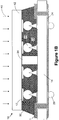
- Figure 1B depicts the device 10 at the point of fabrication wherein the die 12 has been conductively coupled to the substrate 14 by virtue of the conductive engagement between the piercing bond structures 22 and the solder balls 16.
- the piercing bond structures 22 pierce the oxide layer 20 and the solder ball 16 to thereby establish this conductive connection.
- Figure 1B depicts an illustrative standoff structure 34 that may be employed if desired or needed to ensure that the die 12 is positioned a fixed distance from the substrate 14.
- the device 10 is heated and an illustrative downforce 40 is applied.
- the magnitude of the downforce 40 may vary depending upon the particular application. In one illustrative embodiment, the downforce 40 may range from approximately 2-12 kg. In some specific applications, a downforce 40 of approximately 8 kg may be employed.
- the device 10 is heated to a temperature above the melting point of the material of the solder ball 16, e.g., to a temperature ranging from approximately 190-210°C.
- the downforce 40 may be applied for a duration of 0.5-2 seconds, depending on the particular application.
- the article entitled " Instantaneous Fluxless Bonding of Au with Pb-Sn Solder in Ambient Atmosphere," Journal of Applied Physics, Vol. 98, 034904 (2005 ) is hereby incorporated by reference in its entirety.
- Figures 1C-1D are enlarged views of an illustrative solder ball 16 and piercing bond structure 22 prior to engagement ( Figure 1C ) and after engagement ( Figure ID).
- the piercing bond structure 22 has one or more anti-oxidation layers 23 formed on the structure 22 to prevent an oxide film from forming on the piercing bond structure 22.
- the anti-oxidation layer 23 comprises a layer of gold 23A and a layer of nickel 23B.
- the layer of gold 23A may have a thickness of approximately 2.5 ⁇ m, while the layer of nickel 23B may have a thickness of approximately 0.3 ⁇ m.
- Figures 2A-2B schematically depict the reduced pitch between adjacent conductive structures that may result by use of the piercing bond structures 22 disclosed herein.
- Figure 2A schematically depicts an illustrative conductive bond structures 90 that are commonly formed using known techniques.
- the conventional bond structures 90 have a substantially planar upper or contact surface 92.
- the width of the contact surface 92 is designated "A”
- the width of the sloped sidewalls 94 due to the isotropic nature of the etching process used to form the structures 90, is designated as "B”
- the spacing between the structures 90 is designated as "C.”
- the pitch "P" for the conductive structure 90 would be A + 2B + C.
- the pitch ("P1") between the piercing bond structures 22 shown in Figure 2B would be equal to 2B + C.
- the pitch between conductive bonding structures may be substantially less as compared to prior art devices that employ bonding structures having a substantially planar or non-piercing upper surface 92, as shown in Figure 2A .
- the pitch "P1" may be approximately 60 ⁇ m minimum.
- the methodologies and piercing bond structures 22 disclosed herein may be employed with solder balls 16A, 16B, 16C of differing sizes.
- the piercing bond structures 22 described herein may be employed with a vast variety of different connection technologies and techniques.
- the present subject matter may also be employed to control the offset between the die 12 and the printed circuit board 14.
- the greater the downforce 40 the less the distance between the die 12 and the printed circuit board 14.
- the temperature during the engagement process can also be employed to control the spacing between the die 12 and the printed circuit board 14. In general, the greater the temperature, the less the spacing between the die 12 and the printed circuit board 14.
- the piercing bond structures 22 may have a variety of configurations for the piercing end 22A of the structure 22.
- the piercing end 22A may be pointed, rounded or comprise multiple peaks as depicted on the piercing bond structures 22 in Figure 4 (from left to right).
- Figures 5A-5D depict one illustrative process flow for forming the piercing bond structures 22 described herein.
- a masking layer 80 is formed above a layer of conductive material 82.
- the masking layer 80 may be comprised of a variety of materials, e.g., a photoresist material, and it may be formed using traditional photolithography techniques.
- the layer of conductive material 80 may be comprised of a variety of different materials, e.g., gold, and it may be formed by a variety of known techniques, e.g., plating.
- an anisotropic etching process 84 is performed to partially define conductive structures 86 having sloped sidewalls 87.
- the etching process 84 may be stopped at a point in time such that a portion 88 of the layer of conductive material 80 is not etched completely away. In some applications, stopping the etch process 84 so as to leave a remaining portion 88 of the layer of conductive material 82 may not be required.
- the masking layer 80 is removed, and an isotropic etching process 89 is performed until such time as the piercing bond structures 22 depicted in Figure 5D are formed.
- the piercing bond structures 22 have a substantially triangular cross-sectional configuration and a substantially pointed end 22A.
- the end 22A of the piercing bond structure 22 is generally non-planar or non-flat, but it may take on other configurations.
- Figure 4 depicts various illustrative configurations for the end 22A of the piercing bond structures 22.
Landscapes
- Engineering & Computer Science (AREA)
- Manufacturing & Machinery (AREA)
- Microelectronics & Electronic Packaging (AREA)
- Metallurgy (AREA)
- Electric Connection Of Electric Components To Printed Circuits (AREA)
- Ceramic Engineering (AREA)
- Wire Bonding (AREA)
Abstract
Description
- The present subject matter is generally directed to the field of microelectronic devices and, more particularly, to methods of fluxless micro-piercing of solder balls, and the resulting devices.
- Chip-on-board and board-on-chip (BOC) techniques are used to attach semiconductor dies to an interposer or other carrier substrate such as a printed circuit board (PCB). Attachment can be achieved through flip chip attachment, wirebonding, or tape automated bonding ("TAB"). Flip chip attachment typically utilizes ball grid array (BGA) technology. The BGA component (die) includes conductive external contacts, typically in the form of solder balls or bumps, arranged in a grid pattern on the active surface of the die, which permit the die to be flip chip mounted to an interposer or other carrier substrate (e.g., PCB).
- In a flip chip attachment, the balls of the BGA component are aligned with terminals on the carrier substrate, and connected by reflowing the solder balls. The solder balls can be replaced with a conductive polymer that is cured. A dielectric underfill is then interjected between the flip chip die and the surface of the carrier substance to embed the solder balls and mechanically couple the BGA component to the carrier substrate.
- Wirebonding and TAB attachment generally involve attaching a die by its backside to the surface of a carrier substrate with an appropriate adhesive (e.g., epoxy) or tape. With wirebonding, bond wires are attached to each bond pad on the die and bonded to a corresponding terminal pad on the carrier substrate (e.g., interposer). With TAB, ends of metal leads carried on a flexible insulating tape, such as a polyimide, are attached to the bond pads on the die and to the terminal pads on the carrier substrate. A dielectric (e.g., silicon or epoxy) is generally used to cover the bond wires or metal tape leads to prevent damage.
- Flip chip attachment has provided improved electrical performance and allowed greater packaging density. However, developments in ball grid array technology have produced arrays in which the balls are made smaller and with tighter pitches. As the balls become smaller and are set closer together, it poses problems for the mutual alignment of the conductive bumps on the flip chip die with the bond pads on the substrate or interposer. Flip chip attachment can also lead to high costs and process difficulties. For example, a flip chip mounter is required to accurately align the die to the interposer or substrate.
- In flip chip packaging, solid-state welding, adhesive bonding and soldering are often used for joining the interconnect system. These bonding techniques face numerous assembly challenges. Soldering is the preferred bonding technique, thanks to its high assembly yield, ability to eliminate the probe mark through reflow, allowance for rework after assembly, electrical stability and high tolerance in placement accuracy because of self-alignment effects. However, some challenges still remain for soldering assembly, such as a long processing time and the need for a flux-based removal of oxides and hydrocarbons for solderability. For example, solder balls typically have an oxide layer formed on the outer surface of the ball due to the manufacturing processes employed to manufacture the solder balls in an ambient environment.
- In making conductive connections to such solder balls, a flux is employed due to the presence of the oxide layer, i.e., flux is employed to remove such oxides. Processing time is lengthened by flux application, the vision time required for precise alignment and the need for a reflow process to provide sufficient wetting time for soldering. Flux removal of oxides leaves behind undesirable residues that are deleterious to package reliability. Entrapped residues also cause gross solder voids that can result in premature joint failure. Although chlorofluorocarbons (CFCs) are effective in removing flux residues, they are environmentally hazardous and do not present a long-term solution. Thus, the use of flux and its cleaning processes erects a barrier to flip chip deployment in the packaging and integration of microelectronic, optoelectronic and microelectromechanical systems. Fluxless soldering processes, on the other hand, rely on a controlled atmosphere for the reduction of oxides for soldering, but this is cumbersome in high-volume implementation. Obviously, a method of instantaneous fluxless soldering in ambient atmosphere for flip chip assembly is highly desirable.
- The present subject matter is directed to various methods and devices that may solve, or at least reduce, some or all of the aforementioned problems.
- The subject matter disclosed herein may be understood by reference to the following description taken in conjunction with the accompanying drawings, in which like reference numerals identify like elements, and in which:
-
Figures 1A-1D are various views of an illustrative device described herein; -
Figures 2A-2B depict a reduced pitch that may be achieved using the piercing bond structures disclosed herein; -
Figure 3 depicts the piercing bond structures disclosed herein as engaged with different size solder balls; -
Figure 4 depicts a variety of illustrative end configurations for the piercing bond structures disclosed herein; and -
Figures 5A-5D depict one illustrative process flow for forming the piercing bond structures disclosed herein. - While the subject matter described herein is susceptible to various modifications and alternative forms, specific embodiments thereof have been shown by way of example in the drawings and are herein described in detail. It should be understood, however, that the description herein of specific embodiments is not intended to limit the invention to the particular forms disclosed, but on the contrary, the intention is to cover all modifications, equivalents, and alternatives falling within the spirit and scope of the invention as defined by the appended claims.
- Illustrative embodiments of the present subject matter are described below. In the interest of clarity, not all features of an actual implementation are described in this specification. It will of course be appreciated that in the development of any such actual embodiment, numerous implementation-specific decisions must be made to achieve the developers' specific goals, such as compliance with system-related and business-related constraints, which will vary from one implementation to another. Moreover, it will be appreciated that such a development effort might be complex and time-consuming, but would nevertheless be a routine undertaking for those of ordinary skill in the art having the benefit of this disclosure.
- Although various regions and structures shown in the drawings are depicted as having very precise, sharp configurations and profiles, those skilled in the art recognize that, in reality, these regions and structures are not as precise as indicated in the drawings. Additionally, the relative sizes of the various features and doped regions depicted in the drawings may be exaggerated or reduced as compared to the size of those features or regions on fabricated devices. Nevertheless, the attached drawings are included to describe and explain illustrative examples of the subject matter disclosed herein.
-
Figures 1A-1B depict an illustrative embodiment of adevice 10 in accordance with one aspect of the present subject matter. Thedevice 10 comprises adie 12 that is attached to an interposer orsubstrate 14, e.g., a printed circuit board. The terms "substrate" and "interposer" will be used interchangeably herein and they shall be understood to refer to any type of structure to which an integrated circuit die may be mounted. The die 12 comprises a plurality of schematically depictedsolder balls 16 that are conductively coupled toconductive pads 17. Thesolder balls 16 have anillustrative oxide layer 20, e.g., tin oxide, formed on the outer surface thereof due to the manufacturing processes performed to form thesolder balls 16. A plurality ofpiercing bond structures 22 are formed on thesubstrate 14. Thepiercing bond structures 22 are conductively coupled to illustrative wire traces orlines 24 that extend throughvias 26 formed in thesubstrate 14. Thewiring races 24 are conductively coupled toillustrative contact pads 28 formed on thesubstrate 14. A layer ofdielectric material 30 is also provided to electrically isolate various electrical components on thesubstrate 14. At least one anti-oxidation film 23 (seeFigure 1C ) is provided on thepiercing bond structures 22. -
Figure 1A depicts the situation wherein the die 12 is positioned proximate thesubstrate 14 prior to attachment. The die 12 may be coupled to thesubstrate 14 using a variety of known techniques, e.g., adhesives, epoxies, etc. In the depicted example, an amount ofnon-conductive paste 32 is positioned on thesubstrate 14. A non-conductive film may, in some applications, be applied in lieu of thenon-conductive paste 32. -
Figure 1B depicts thedevice 10 at the point of fabrication wherein the die 12 has been conductively coupled to thesubstrate 14 by virtue of the conductive engagement between thepiercing bond structures 22 and thesolder balls 16. The piercingbond structures 22 pierce theoxide layer 20 and thesolder ball 16 to thereby establish this conductive connection. Also note thatFigure 1B depicts anillustrative standoff structure 34 that may be employed if desired or needed to ensure that thedie 12 is positioned a fixed distance from thesubstrate 14. - In attaching the die 12 to the
substrate 14, thedevice 10 is heated and anillustrative downforce 40 is applied. The magnitude of thedownforce 40 may vary depending upon the particular application. In one illustrative embodiment, thedownforce 40 may range from approximately 2-12 kg. In some specific applications, adownforce 40 of approximately 8 kg may be employed. Thedevice 10 is heated to a temperature above the melting point of the material of thesolder ball 16, e.g., to a temperature ranging from approximately 190-210°C. Thedownforce 40 may be applied for a duration of 0.5-2 seconds, depending on the particular application. The article entitled "Instantaneous Fluxless Bonding of Au with Pb-Sn Solder in Ambient Atmosphere," Journal of Applied Physics, Vol. 98, 034904 (2005) is hereby incorporated by reference in its entirety. -
Figures 1C-1D are enlarged views of anillustrative solder ball 16 and piercingbond structure 22 prior to engagement (Figure 1C ) and after engagement (Figure ID). As mentioned previously, the piercingbond structure 22 has one or moreanti-oxidation layers 23 formed on thestructure 22 to prevent an oxide film from forming on the piercingbond structure 22. In the illustrative example depicted inFigures 1C-1D , theanti-oxidation layer 23 comprises a layer ofgold 23A and a layer ofnickel 23B. Of course, other materials may be employed. The layer ofgold 23A may have a thickness of approximately 2.5 µm, while the layer ofnickel 23B may have a thickness of approximately 0.3 µm. -
Figures 2A-2B schematically depict the reduced pitch between adjacent conductive structures that may result by use of the piercingbond structures 22 disclosed herein.Figure 2A schematically depicts an illustrative conductive bond structures 90 that are commonly formed using known techniques. The conventional bond structures 90 have a substantially planar upper or contact surface 92. InFigure 2A , the width of the contact surface 92 is designated "A," the width of the sloped sidewalls 94, due to the isotropic nature of the etching process used to form the structures 90, is designated as "B" and the spacing between the structures 90 is designated as "C." Thus, the pitch "P" for the conductive structure 90 would be A + 2B + C. In contrast, the pitch ("P1") between the piercingbond structures 22 shown inFigure 2B would be equal to 2B + C. In short, using the techniques and piercingbond structures 22 disclosed herein, the pitch between conductive bonding structures (like the piercingbond structures 22 disclosed herein) may be substantially less as compared to prior art devices that employ bonding structures having a substantially planar or non-piercing upper surface 92, as shown inFigure 2A . For example, using the piercingbond structures 22 described herein, the pitch "P1" may be approximately 60 µm minimum. - As shown in
Figure 3 , the methodologies and piercingbond structures 22 disclosed herein may be employed withsolder balls bond structures 22 described herein may be employed with a vast variety of different connection technologies and techniques. - The present subject matter may also be employed to control the offset between the die 12 and the printed
circuit board 14. In general, all other things being equal, the greater thedownforce 40, the less the distance between the die 12 and the printedcircuit board 14. The temperature during the engagement process can also be employed to control the spacing between the die 12 and the printedcircuit board 14. In general, the greater the temperature, the less the spacing between the die 12 and the printedcircuit board 14. - As shown in
Figure 4 , the piercingbond structures 22 may have a variety of configurations for the piercingend 22A of thestructure 22. For example, the piercingend 22A may be pointed, rounded or comprise multiple peaks as depicted on the piercingbond structures 22 inFigure 4 (from left to right). -
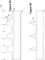
Figures 5A-5D depict one illustrative process flow for forming the piercingbond structures 22 described herein. Initially, as shown inFigure 5A , amasking layer 80 is formed above a layer ofconductive material 82. Themasking layer 80 may be comprised of a variety of materials, e.g., a photoresist material, and it may be formed using traditional photolithography techniques. The layer ofconductive material 80 may be comprised of a variety of different materials, e.g., gold, and it may be formed by a variety of known techniques, e.g., plating. - As shown in
Figure 5B , ananisotropic etching process 84 is performed to partially defineconductive structures 86 having slopedsidewalls 87. Theetching process 84 may be stopped at a point in time such that aportion 88 of the layer ofconductive material 80 is not etched completely away. In some applications, stopping theetch process 84 so as to leave a remainingportion 88 of the layer ofconductive material 82 may not be required. As shown inFigure 5C , themasking layer 80 is removed, and anisotropic etching process 89 is performed until such time as the piercingbond structures 22 depicted inFigure 5D are formed. Note that, in the illustrative embodiment depicted herein, the piercingbond structures 22 have a substantially triangular cross-sectional configuration and a substantiallypointed end 22A. Theend 22A of the piercingbond structure 22 is generally non-planar or non-flat, but it may take on other configurations. For example,Figure 4 depicts various illustrative configurations for theend 22A of the piercingbond structures 22. - The particular embodiments disclosed above are illustrative only, as the invention may be modified and practiced in different but equivalent manners apparent to those skilled in the art having the benefit of the teachings herein. For example, the process steps set forth above may be performed in a different order. Furthermore, no limitations are intended to the details of construction or design herein shown, other than as described in the claims below. It is therefore evident that the particular embodiments disclosed above may be altered or modified and all such variations are considered within the scope and spirit of the invention. Accordingly, the protection sought herein is as set forth in the claims below.
-
- 1. A method, comprising:
- forming a layer of conductive material above a substrate;
- forming a masking layer above the layer of conductive material;
- performing a first etching process on the layer of conductive material with the masking layer in place;
- removing the masking layer; and
- after removing the masking layer, performing an isotropic etching process on the layer of conductive material to thereby define a plurality of piercing bond structures positioned on the substrate.
- 2. The method of embodiment 1, further comprising:
- providing an integrated circuit die having a plurality of solder balls, each of which have a layer of oxide on an outer surface of the ball;
- heating at least the solder balls; and
- applying a force that causes each of the plurality of piercing bond structures to pierce one of the solder balls with the oxide layer formed thereon and thereby establish a conductive connection between the solder ball and the piercing bond structure.
- 3. The method of embodiment 2, wherein the steps recited in embodiment 2 are performed in an ambient, oxygen-containing environment.
- 4. The method of embodiment 2, wherein heating at least the solder balls comprises heating at least the solder balls to a temperature that is above a melting point of a material of the solder balls.
- 5. The method of embodiment 2, wherein applying the force comprises applying a force ranging from 5-12 Kg for a duration ranging from 0.5-2 seconds.
- 6. The method of embodiment 2, wherein the steps recited in embodiment 2 are performed without applying a flux to the plurality of solder balls.
- 7. The method of embodiment 1, wherein the first etching process is an anisotropic etching process.
- 8. The method of embodiment 3, wherein the substrate comprises a printed circuit board.
- 9. The method of embodiment 1, wherein each of the plurality of piercing bond structures has a substantially triangular cross-sectional configuration.
- 10. A method, comprising:
- providing an integrated circuit die having a plurality of solder balls, each of which have a layer of oxide on an outer surface of the ball;
- performing a heating process to heat at least the solder balls; and
- applying a force that causes each of a plurality of piercing bond structures on a substrate to pierce one of the solder balls and its associated oxide layer to thereby establish a conductive connection between the solder ball and the piercing bond structure.
- 11. The method of
embodiment 10, wherein the steps recited inclaim 10 are performed in an ambient, oxygen-containing environment. - 12. The method of
embodiment 10, wherein performing the hearing process comprises heating at least the solder balls to a temperature that is above a melting point of a material of the solder balls. - 13. The method of
embodiment 10, wherein applying the force comprises applying a force ranging from 5-12 Kg for a duration ranging from 0.5-2 seconds. - 14. The method of embodiment 11, wherein the steps recited in
embodiment 10 are performed without applying a flux to the plurality of solder balls. - 15. The method of
embodiment 12, wherein the substrate comprises a printed circuit board. - 16. The method of embodiment 13, wherein each of the plurality of piercing bond structures has a substantially triangular cross-sectional configuration.
- 17. A device, comprising:
- an integrated circuit die having a plurality of solder balls that are conductively coupled to bond pads on the die, each of the solder balls having a layer of oxide on an outer surface thereof; and
- a substrate comprising a plurality of piercing bond structures, each of the piercing bond structures penetrating and extending at least partially into a corresponding solder ball to thereby establish a conductive connection between the solder ball and the piercing bond structure, the piercing bond structure penetrating the layer of oxide.
- 18. The device of
embodiment 17, wherein the piercing bond structures have a non-flat end. - 19. The device of
embodiment 17, wherein each of the piercing bond structures comprises at least one anti-oxidation layer formed on an outer surface of the piercing bond structure. - 20. The device of embodiment 19, wherein the at least one anti-oxidation layer comprises a plurality of layers of material.
- 21. The device of
embodiment 20, wherein the plurality of layers comprises a layer comprising gold formed on an exposed surface of the piercing bond structure and a layer comprising nickel formed on the layer comprising gold. - 22. The device of
embodiment 17, wherein the plurality of piercing bond structures has a substantially triangular cross-sectional configuration.
Claims (11)
- A device, comprising:an integrated circuit die (12) having a plurality of solder balls (16) that are conductively coupled to bond pads (17) on the die (12), each of the solder balls (16) having a layer (20) of oxide on an outer surface thereof;a substrate (14) comprising a plurality of piercing bond structures (22), each of the piercing bond structures (22) penetrating and extending at least partially into a corresponding solder ball (16) to thereby establish a conductive connection between the solder ball (16) and the piercing bond structure (22), the piercing bond structure (22) penetrating the layer of oxide (20); anda non-conductive paste (32) coupling the integrated circuit die (12) to the substrate (14).
- The device of claim 1, wherein each of the plurality of piercing bond structures has a non-flat end.
- The device of claim 1, wherein each of the piercing bond structures (22) comprises at least one anti-oxidation layer (23) formed on an outer surface of the piercing bond structure.
- The device of claim 3, wherein the at least one anti-oxidation layer comprises a plurality of layers of material.
- The device of claim 4, wherein the plurality of layers comprises a layer comprising gold formed on an exposed surface of the piercing bond structure and a layer comprising nickel formed on the layer comprising gold.
- The device of claim 1, wherein each of the plurality of piercing bond structures has a substantially triangular cross-sectional configuration.
- The device of claim 1, wherein each of the plurality of piercing bond structures has a multiple-peak cross section.
- The device of claim 1, further comprising a standoff structure between the integrated circuit die and the substrate.
- The device of claim 1, wherein each of the plurality of piercing bond structures has an outer surface that surrounds a solid core of conductive material, and wherein the outer surface includes an anti-oxidation material.
- The device of claim 9, wherein the anti-oxidation material includes a first layer with a first thickness of about 2.5 µm and a second layer with a second thickness of about 0.3 µm.
- The device of claim 10, wherein the anti-oxidation material includes a first layer of gold and a second layer of nickel.
Applications Claiming Priority (3)
| Application Number | Priority Date | Filing Date | Title |
|---|---|---|---|
| US11/958,842 US7749887B2 (en) | 2007-12-18 | 2007-12-18 | Methods of fluxless micro-piercing of solder balls, and resulting devices |
| PCT/US2008/085433 WO2009079214A1 (en) | 2007-12-18 | 2008-12-03 | Methods of fluxless micro-piercing of solder balls, and resulting devices |
| EP08862313.7A EP2232964B1 (en) | 2007-12-18 | 2008-12-03 | Method for forming piercing bond structures on a substrate |
Related Parent Applications (1)
| Application Number | Title | Priority Date | Filing Date |
|---|---|---|---|
| EP08862313.7A Division EP2232964B1 (en) | 2007-12-18 | 2008-12-03 | Method for forming piercing bond structures on a substrate |
Publications (2)
| Publication Number | Publication Date |
|---|---|
| EP3410830A1 true EP3410830A1 (en) | 2018-12-05 |
| EP3410830B1 EP3410830B1 (en) | 2025-09-10 |
Family
ID=40329135
Family Applications (2)
| Application Number | Title | Priority Date | Filing Date |
|---|---|---|---|
| EP08862313.7A Active EP2232964B1 (en) | 2007-12-18 | 2008-12-03 | Method for forming piercing bond structures on a substrate |
| EP18183518.2A Active EP3410830B1 (en) | 2007-12-18 | 2008-12-03 | Device comprising an integrated circuit die connected to a substrate |
Family Applications Before (1)
| Application Number | Title | Priority Date | Filing Date |
|---|---|---|---|
| EP08862313.7A Active EP2232964B1 (en) | 2007-12-18 | 2008-12-03 | Method for forming piercing bond structures on a substrate |
Country Status (6)
| Country | Link |
|---|---|
| US (5) | US7749887B2 (en) |
| EP (2) | EP2232964B1 (en) |
| KR (1) | KR101156819B1 (en) |
| CN (1) | CN101904230B (en) |
| TW (1) | TWI487045B (en) |
| WO (1) | WO2009079214A1 (en) |
Families Citing this family (24)
| Publication number | Priority date | Publication date | Assignee | Title |
|---|---|---|---|---|
| US7749887B2 (en) | 2007-12-18 | 2010-07-06 | Micron Technology, Inc. | Methods of fluxless micro-piercing of solder balls, and resulting devices |
| US8424748B2 (en) * | 2009-12-21 | 2013-04-23 | Intel Corporation | Solder in cavity interconnection technology |
| TW201208007A (en) * | 2010-08-02 | 2012-02-16 | Advanced Semiconductor Eng | Semiconductor package |
| TWI542260B (en) * | 2010-12-24 | 2016-07-11 | Lg伊諾特股份有限公司 | Printed circuit board and method for manufacturing the same |
| DE102011000866A1 (en) * | 2011-02-22 | 2012-08-23 | Friedrich-Alexander-Universität Erlangen-Nürnberg | Electrical component with an electrical connection arrangement and method for its production |
| US8508045B2 (en) | 2011-03-03 | 2013-08-13 | Broadcom Corporation | Package 3D interconnection and method of making same |
| US9064781B2 (en) * | 2011-03-03 | 2015-06-23 | Broadcom Corporation | Package 3D interconnection and method of making same |
| US9263412B2 (en) | 2012-03-09 | 2016-02-16 | Taiwan Semiconductor Manufacturing Company, Ltd. | Packaging methods and packaged semiconductor devices |
| US20130234317A1 (en) * | 2012-03-09 | 2013-09-12 | Taiwan Semiconductor Manufacturing Company, Ltd. | Packaging Methods and Packaged Semiconductor Devices |
| US9768137B2 (en) | 2012-04-30 | 2017-09-19 | Taiwan Semiconductor Manufacturing Company, Ltd. | Stud bump structure for semiconductor package assemblies |
| US20130301561A1 (en) * | 2012-05-08 | 2013-11-14 | Futurewei Technologies, Inc. | System and Method for Antenna Port Association |
| US9779969B2 (en) * | 2014-03-13 | 2017-10-03 | Taiwan Semiconductor Manufacturing Co., Ltd. | Package structure and manufacturing method |
| EP3187299B1 (en) * | 2014-08-29 | 2020-10-14 | Senju Metal Industry Co., Ltd | Solder material, use of solder material, and production method for solder material |
| KR102274742B1 (en) * | 2014-10-06 | 2021-07-07 | 삼성전자주식회사 | PACKAGE ON PACKAGE(PoP) AND COMPUTING DEVICE HAVING THE PoP |
| US9576922B2 (en) * | 2015-05-04 | 2017-02-21 | Globalfoundries Inc. | Silver alloying post-chip join |
| US10468363B2 (en) * | 2015-08-10 | 2019-11-05 | X-Celeprint Limited | Chiplets with connection posts |
| US11495560B2 (en) * | 2015-08-10 | 2022-11-08 | X Display Company Technology Limited | Chiplets with connection posts |
| WO2017171857A1 (en) * | 2016-04-01 | 2017-10-05 | Intel Corporation | Systems and methods for replaceable ball grid array (bga) packages on board substrates |
| US11064609B2 (en) | 2016-08-04 | 2021-07-13 | X Display Company Technology Limited | Printable 3D electronic structure |
| US11131689B2 (en) | 2017-05-25 | 2021-09-28 | International Business Machines Corporation | Low-force wafer test probes |
| US11444048B2 (en) * | 2017-10-05 | 2022-09-13 | Texas Instruments Incorporated | Shaped interconnect bumps in semiconductor devices |
| US10989735B2 (en) | 2019-08-21 | 2021-04-27 | Facebook Technologies, Llc | Atomic force microscopy tips for interconnection |
| JP7316192B2 (en) * | 2019-10-29 | 2023-07-27 | タイコエレクトロニクスジャパン合同会社 | socket |
| US12015001B2 (en) * | 2022-03-15 | 2024-06-18 | Taiwan Semiconductor Manufacturing Company Ltd. | Bonding structure and method thereof |
Citations (3)
| Publication number | Priority date | Publication date | Assignee | Title |
|---|---|---|---|---|
| US6335571B1 (en) * | 1997-07-21 | 2002-01-01 | Miguel Albert Capote | Semiconductor flip-chip package and method for the fabrication thereof |
| US20030216023A1 (en) * | 1997-03-26 | 2003-11-20 | Wark James M. | Projected contact structures for engaging bumped semiconductor devices and methods of making the same |
| EP1797749A1 (en) * | 2004-10-04 | 2007-06-20 | Commissariat A L'energie Atomique | Component provided with an assembly of hard conductive microtips and method for electrical connection of said component and a component provided with ductile conductive protrusions |
Family Cites Families (96)
| Publication number | Priority date | Publication date | Assignee | Title |
|---|---|---|---|---|
| US4483720A (en) * | 1981-11-27 | 1984-11-20 | S R I International | Process for applying thermal barrier coatings to metals |
| US5134460A (en) * | 1986-08-11 | 1992-07-28 | International Business Machines Corporation | Aluminum bump, reworkable bump, and titanium nitride structure for tab bonding |
| US4912545A (en) * | 1987-09-16 | 1990-03-27 | Irvine Sensors Corporation | Bonding of aligned conductive bumps on adjacent surfaces |
| US4865245A (en) * | 1987-09-24 | 1989-09-12 | Santa Barbara Research Center | Oxide removal from metallic contact bumps formed on semiconductor devices to improve hybridization cold-welds |
| US5634267A (en) * | 1991-06-04 | 1997-06-03 | Micron Technology, Inc. | Method and apparatus for manufacturing known good semiconductor die |
| US5071787A (en) * | 1989-03-14 | 1991-12-10 | Kabushiki Kaisha Toshiba | Semiconductor device utilizing a face-down bonding and a method for manufacturing the same |
| US4930001A (en) * | 1989-03-23 | 1990-05-29 | Hughes Aircraft Company | Alloy bonded indium bumps and methods of processing same |
| US4989400A (en) * | 1989-09-01 | 1991-02-05 | Snapper Power Equipment, Division Of Fuqua Industries, Inc. | Disposable bag and mounting apparatus for a lawn mower |
| US5471151A (en) * | 1990-02-14 | 1995-11-28 | Particle Interconnect, Inc. | Electrical interconnect using particle enhanced joining of metal surfaces |
| US5341980A (en) * | 1990-02-19 | 1994-08-30 | Hitachi, Ltd. | Method of fabricating electronic circuit device and apparatus for performing the same method |
| US5878943A (en) * | 1990-02-19 | 1999-03-09 | Hitachi, Ltd. | Method of fabricating an electronic circuit device and apparatus for performing the method |
| US5207585A (en) * | 1990-10-31 | 1993-05-04 | International Business Machines Corporation | Thin interface pellicle for dense arrays of electrical interconnects |
| US5585282A (en) * | 1991-06-04 | 1996-12-17 | Micron Technology, Inc. | Process for forming a raised portion on a projecting contact for electrical testing of a semiconductor |
| US5592736A (en) * | 1993-09-03 | 1997-01-14 | Micron Technology, Inc. | Fabricating an interconnect for testing unpackaged semiconductor dice having raised bond pads |
| US5326428A (en) * | 1993-09-03 | 1994-07-05 | Micron Semiconductor, Inc. | Method for testing semiconductor circuitry for operability and method of forming apparatus for testing semiconductor circuitry for operability |
| DE4442960C1 (en) * | 1994-12-02 | 1995-12-21 | Fraunhofer Ges Forschung | Solder bump used in mfr. of semiconductor chips |
| JP2830903B2 (en) * | 1995-07-21 | 1998-12-02 | 日本電気株式会社 | Method for manufacturing semiconductor device |
| JPH09148693A (en) * | 1995-11-20 | 1997-06-06 | Shinko Electric Ind Co Ltd | Substrate for flip chip mounting and method of manufacturing the same |
| US5719440A (en) | 1995-12-19 | 1998-02-17 | Micron Technology, Inc. | Flip chip adaptor package for bare die |
| US5889326A (en) * | 1996-02-27 | 1999-03-30 | Nec Corporation | Structure for bonding semiconductor device to substrate |
| KR100197074B1 (en) * | 1996-04-30 | 1999-06-15 | 김춘호 | Package Structure and Method of Chip Device |
| JPH1032223A (en) * | 1996-07-15 | 1998-02-03 | Mitsubishi Electric Corp | Semiconductor device |
| US6179198B1 (en) * | 1996-09-18 | 2001-01-30 | Matsushita Electric Industrial Co., Ltd. | Method of soldering bumped work by partially penetrating the oxide film covering the solder bumps |
| US5801452A (en) | 1996-10-25 | 1998-09-01 | Micron Technology, Inc. | Multi chip module including semiconductor wafer or dice, interconnect substrate, and alignment member |
| JP3553300B2 (en) * | 1996-12-02 | 2004-08-11 | 富士通株式会社 | Semiconductor device manufacturing method and semiconductor device mounting method |
| US5952840A (en) | 1996-12-31 | 1999-09-14 | Micron Technology, Inc. | Apparatus for testing semiconductor wafers |
| JPH10303252A (en) * | 1997-04-28 | 1998-11-13 | Nec Kansai Ltd | Semiconductor device |
| US5796163A (en) * | 1997-05-23 | 1998-08-18 | Amkor Technology, Inc. | Solder ball joint |
| US6083773A (en) | 1997-09-16 | 2000-07-04 | Micron Technology, Inc. | Methods of forming flip chip bumps and related flip chip bump constructions |
| SG71734A1 (en) * | 1997-11-21 | 2000-04-18 | Inst Materials Research & Eng | Area array stud bump flip chip and assembly process |
| US6130148A (en) * | 1997-12-12 | 2000-10-10 | Farnworth; Warren M. | Interconnect for semiconductor components and method of fabrication |
| US6140827A (en) * | 1997-12-18 | 2000-10-31 | Micron Technology, Inc. | Method and apparatus for testing bumped die |
| KR100274991B1 (en) * | 1997-12-26 | 2001-01-15 | 윤종용 | Csp and mounting method thereof, and jig for forming patterns on electrodes of csp |
| US6426636B1 (en) * | 1998-02-11 | 2002-07-30 | International Business Machines Corporation | Wafer probe interface arrangement with nonresilient probe elements and support structure |
| US6337445B1 (en) * | 1998-03-16 | 2002-01-08 | Texas Instruments Incorporated | Composite connection structure and method of manufacturing |
| JPH11312711A (en) * | 1998-04-30 | 1999-11-09 | Murata Mfg Co Ltd | How to connect electronic components |
| US6537854B1 (en) * | 1999-05-24 | 2003-03-25 | Industrial Technology Research Institute | Method for bonding IC chips having multi-layered bumps with corrugated surfaces and devices formed |
| US6562545B1 (en) | 1999-09-17 | 2003-05-13 | Micron Technology, Inc. | Method of making a socket assembly for use with a solder ball |
| US6497943B1 (en) * | 2000-02-14 | 2002-12-24 | International Business Machines Corporation | Surface metal balancing to reduce chip carrier flexing |
| US6529027B1 (en) | 2000-03-23 | 2003-03-04 | Micron Technology, Inc. | Interposer and methods for fabricating same |
| TW445612B (en) * | 2000-08-03 | 2001-07-11 | Siliconware Precision Industries Co Ltd | Solder ball array structure to control the degree of collapsing |
| US6537482B1 (en) | 2000-08-08 | 2003-03-25 | Micron Technology, Inc. | Underfill and encapsulation of carrier substrate-mounted flip-chip components using stereolithography |
| US6641406B1 (en) * | 2000-11-03 | 2003-11-04 | Cray Inc. | Flexible connector for high density circuit applications |
| US6795250B2 (en) * | 2000-12-29 | 2004-09-21 | Lenticlear Lenticular Lens, Inc. | Lenticular lens array |
| SG99877A1 (en) | 2001-01-04 | 2003-11-27 | Inst Materials Research & Eng | Forming an electrical contact on an electronic component |
| JP2002222832A (en) * | 2001-01-29 | 2002-08-09 | Nec Corp | Semiconductor device and semiconductor element mounting method |
| JP2002344126A (en) | 2001-05-14 | 2002-11-29 | Nec Corp | Mounting structure of printed circuit board and LSI chip |
| SG104293A1 (en) | 2002-01-09 | 2004-06-21 | Micron Technology Inc | Elimination of rdl using tape base flip chip on flex for die stacking |
| JP4044769B2 (en) * | 2002-02-22 | 2008-02-06 | 富士通株式会社 | Semiconductor device substrate, manufacturing method thereof, and semiconductor package |
| SG115459A1 (en) | 2002-03-04 | 2005-10-28 | Micron Technology Inc | Flip chip packaging using recessed interposer terminals |
| US6975035B2 (en) | 2002-03-04 | 2005-12-13 | Micron Technology, Inc. | Method and apparatus for dielectric filling of flip chip on interposer assembly |
| US6583517B1 (en) * | 2002-04-09 | 2003-06-24 | International Business Machines Corporation | Method and structure for joining two substrates with a low melt solder joint |
| KR100597734B1 (en) | 2002-06-25 | 2006-07-07 | 삼성전자주식회사 | Memory drive and control method |
| US6669173B1 (en) | 2002-09-27 | 2003-12-30 | James R. Dunn | Dual purpose pneumatic floor covering device |
| US7015590B2 (en) * | 2003-01-10 | 2006-03-21 | Samsung Electronics Co., Ltd. | Reinforced solder bump structure and method for forming a reinforced solder bump |
| JP2004265888A (en) * | 2003-01-16 | 2004-09-24 | Sony Corp | Semiconductor device and manufacturing method thereof |
| TWI233190B (en) * | 2003-02-11 | 2005-05-21 | Via Tech Inc | Structure of chip package and process thereof |
| US7008867B2 (en) * | 2003-02-21 | 2006-03-07 | Aptos Corporation | Method for forming copper bump antioxidation surface |
| TWI226689B (en) * | 2003-02-25 | 2005-01-11 | Via Tech Inc | Chip package and process for forming the same |
| KR20040078807A (en) * | 2003-03-05 | 2004-09-13 | 삼성전자주식회사 | Ball Grid Array Stack Package |
| US7271497B2 (en) * | 2003-03-10 | 2007-09-18 | Fairchild Semiconductor Corporation | Dual metal stud bumping for flip chip applications |
| TW591780B (en) * | 2003-03-21 | 2004-06-11 | Univ Nat Central | Flip chip Au bump structure and method of manufacturing the same |
| US20050120553A1 (en) * | 2003-12-08 | 2005-06-09 | Brown Dirk D. | Method for forming MEMS grid array connector |
| US7244125B2 (en) * | 2003-12-08 | 2007-07-17 | Neoconix, Inc. | Connector for making electrical contact at semiconductor scales |
| JP4104490B2 (en) * | 2003-05-21 | 2008-06-18 | オリンパス株式会社 | Manufacturing method of semiconductor device |
| US6849944B2 (en) * | 2003-05-30 | 2005-02-01 | Texas Instruments Incorporated | Using a supporting structure to control collapse of a die towards a die pad during a reflow process for coupling the die to the die pad |
| JP3994924B2 (en) * | 2003-06-02 | 2007-10-24 | セイコーエプソン株式会社 | Circuit board manufacturing method |
| KR100604334B1 (en) * | 2003-11-25 | 2006-08-08 | (주)케이나인 | Flip Chip Bondig Method for Enhancing the Performance of Connection in Flip Chip Packaging Process |
| FR2876243B1 (en) * | 2004-10-04 | 2007-01-26 | Commissariat Energie Atomique | DUCTILE BURST CONDUCTIVE PROTUBERANCE COMPONENT AND METHOD FOR ELECTRICAL CONNECTION BETWEEN THIS COMPONENT AND A COMPONENT HAVING HARD CONDUCTIVE POINTS |
| JP2006107854A (en) | 2004-10-04 | 2006-04-20 | Nec Electronics Corp | Ic socket |
| US8294279B2 (en) * | 2005-01-25 | 2012-10-23 | Megica Corporation | Chip package with dam bar restricting flow of underfill |
| JP2008535225A (en) * | 2005-03-25 | 2008-08-28 | スタッツ チップパック リミテッド | Flip chip wiring having a narrow wiring portion on a substrate |
| US7691675B2 (en) * | 2005-10-24 | 2010-04-06 | Hewlett-Packard Development Company, L.P. | Encapsulating electrical connections |
| DE102006001254B4 (en) * | 2005-11-30 | 2015-03-19 | Globalfoundries Inc. | Method for producing solder balls with a stable oxide layer by controlling the melting environment |
| US8067267B2 (en) | 2005-12-23 | 2011-11-29 | Tessera, Inc. | Microelectronic assemblies having very fine pitch stacking |
| US20080185705A1 (en) * | 2005-12-23 | 2008-08-07 | Tessera, Inc. | Microelectronic packages and methods therefor |
| TWI282612B (en) * | 2006-03-20 | 2007-06-11 | Phoenix Prec Technology Corp | Method for fabricating a metal protecting layer on electrically connecting pad of circuit board |
| US7674651B2 (en) * | 2006-12-26 | 2010-03-09 | International Business Machines Corporation | Mounting method for semiconductor parts on circuit substrate |
| JP4431606B2 (en) * | 2007-10-05 | 2010-03-17 | シャープ株式会社 | Semiconductor device, semiconductor device mounting method, and semiconductor device mounting structure |
| US7749887B2 (en) * | 2007-12-18 | 2010-07-06 | Micron Technology, Inc. | Methods of fluxless micro-piercing of solder balls, and resulting devices |
| JP2009158593A (en) * | 2007-12-25 | 2009-07-16 | Tessera Interconnect Materials Inc | Bump structure and manufacturing method thereof |
| US7838954B2 (en) * | 2008-01-16 | 2010-11-23 | International Business Machines Corporation | Semiconductor structure with solder bumps |
| US7863724B2 (en) * | 2008-02-12 | 2011-01-04 | International Business Machines Corporation | Circuit substrate having post-fed die side power supply connections |
| KR100969412B1 (en) * | 2008-03-18 | 2010-07-14 | 삼성전기주식회사 | Multilayer printed circuit board and its manufacturing method |
| TWI405361B (en) * | 2008-12-31 | 2013-08-11 | 財團法人工業技術研究院 | Thermoelectric element and its process, wafer stack structure and chip package structure |
| US8922004B2 (en) * | 2010-06-11 | 2014-12-30 | Taiwan Semiconductor Manufacturing Company, Ltd. | Copper bump structures having sidewall protection layers |
| KR101736984B1 (en) * | 2010-09-16 | 2017-05-17 | 삼성전자 주식회사 | Print circuit board having hexagonal bump pad for substrate of semiconductor package and semiconductor package having the same |
| FR2971081B1 (en) * | 2011-02-02 | 2013-01-25 | Commissariat Energie Atomique | METHOD FOR MANUFACTURING TWO SUBSTRATES CONNECTED BY AT LEAST ONE MECHANICAL AND ELECTRICALLY CONDUCTIVE CONNECTION OBTAINED |
| US8288871B1 (en) * | 2011-04-27 | 2012-10-16 | Taiwan Semiconductor Manufacturing Company, Ltd. | Reduced-stress bump-on-trace (BOT) structures |
| US9200883B2 (en) * | 2011-05-05 | 2015-12-01 | International Business Machines Corporation | Transferable probe tips |
| TWI576869B (en) * | 2014-01-24 | 2017-04-01 | 精材科技股份有限公司 | Passive component structure and manufacturing method thereof |
| US9070586B1 (en) * | 2014-02-22 | 2015-06-30 | International Business Machines Corporation | Method of forming surface protrusions on an article and the article with the protrusions attached |
| US10330701B2 (en) * | 2014-02-22 | 2019-06-25 | International Business Machines Corporation | Test probe head for full wafer testing |
| KR102212827B1 (en) * | 2014-06-30 | 2021-02-08 | 엘지이노텍 주식회사 | Pcb, package substrate and a manufacturing method thereof |
| US9929230B2 (en) * | 2016-03-11 | 2018-03-27 | International Business Machines Corporation | Air-core inductors and transformers |
| US10001508B2 (en) * | 2016-06-17 | 2018-06-19 | International Business Machines Corporation | Integrated self-coining probe |
-
2007
- 2007-12-18 US US11/958,842 patent/US7749887B2/en active Active
-
2008
- 2008-12-03 EP EP08862313.7A patent/EP2232964B1/en active Active
- 2008-12-03 CN CN200880121032.XA patent/CN101904230B/en active Active
- 2008-12-03 KR KR1020107012500A patent/KR101156819B1/en active Active
- 2008-12-03 WO PCT/US2008/085433 patent/WO2009079214A1/en not_active Ceased
- 2008-12-03 EP EP18183518.2A patent/EP3410830B1/en active Active
- 2008-12-11 TW TW097148258A patent/TWI487045B/en active
-
2010
- 2010-06-30 US US12/827,476 patent/US8436478B2/en active Active
-
2013
- 2013-04-30 US US13/873,509 patent/US8669173B2/en active Active
-
2014
- 2014-03-07 US US14/201,031 patent/US10163840B2/en active Active
-
2018
- 2018-09-21 US US16/138,074 patent/US10515918B2/en active Active
Patent Citations (3)
| Publication number | Priority date | Publication date | Assignee | Title |
|---|---|---|---|---|
| US20030216023A1 (en) * | 1997-03-26 | 2003-11-20 | Wark James M. | Projected contact structures for engaging bumped semiconductor devices and methods of making the same |
| US6335571B1 (en) * | 1997-07-21 | 2002-01-01 | Miguel Albert Capote | Semiconductor flip-chip package and method for the fabrication thereof |
| EP1797749A1 (en) * | 2004-10-04 | 2007-06-20 | Commissariat A L'energie Atomique | Component provided with an assembly of hard conductive microtips and method for electrical connection of said component and a component provided with ductile conductive protrusions |
Non-Patent Citations (1)
| Title |
|---|
| "Instantaneous Fluxless Bonding of Au with Pb-Sn Solder in Ambient Atmosphere", JOURNAL OF APPLIED PHYSICS, vol. 98, 2005, pages 034904 |
Also Published As
| Publication number | Publication date |
|---|---|
| EP2232964A1 (en) | 2010-09-29 |
| US20090152719A1 (en) | 2009-06-18 |
| TW200937547A (en) | 2009-09-01 |
| US8669173B2 (en) | 2014-03-11 |
| US10515918B2 (en) | 2019-12-24 |
| US10163840B2 (en) | 2018-12-25 |
| CN101904230A (en) | 2010-12-01 |
| US20190019774A1 (en) | 2019-01-17 |
| US20130234328A1 (en) | 2013-09-12 |
| US20100264541A1 (en) | 2010-10-21 |
| TWI487045B (en) | 2015-06-01 |
| US7749887B2 (en) | 2010-07-06 |
| EP2232964B1 (en) | 2018-08-01 |
| US20150008577A1 (en) | 2015-01-08 |
| KR101156819B1 (en) | 2012-06-18 |
| US8436478B2 (en) | 2013-05-07 |
| WO2009079214A1 (en) | 2009-06-25 |
| KR20100077049A (en) | 2010-07-06 |
| EP3410830B1 (en) | 2025-09-10 |
| CN101904230B (en) | 2015-07-29 |
Similar Documents
| Publication | Publication Date | Title |
|---|---|---|
| US10515918B2 (en) | Methods of fluxless micro-piercing of solder balls, and resulting devices | |
| US6774497B1 (en) | Flip-chip assembly with thin underfill and thick solder mask | |
| US6046910A (en) | Microelectronic assembly having slidable contacts and method for manufacturing the assembly | |
| US9159665B2 (en) | Flip chip interconnection having narrow interconnection sites on the substrate | |
| KR100645418B1 (en) | Mounting substrate | |
| TWI546924B (en) | Method and related apparatus for manufacturing an electronic device including an open cover layer | |
| US12438067B2 (en) | Flip chip self-alignment features for substrate and leadframe applications and method of manufacturing the flip chip self-alignment features | |
| JP2010118534A (en) | Semiconductor device and method of manufacturing same | |
| JP2009099669A (en) | Electronic component mounting structure and mounting method | |
| JP3847602B2 (en) | Stacked semiconductor device, method for manufacturing the same, motherboard mounted with semiconductor device, and method for manufacturing motherboard mounted with semiconductor device | |
| TWI546922B (en) | Semiconductor device and method of manufacturing same | |
| US8168525B2 (en) | Electronic part mounting board and method of mounting the same | |
| JPH1167823A (en) | Manufacturing method of wiring substrate with bump and semiconductor package | |
| JP4483131B2 (en) | Mounting structure and mounting method thereof | |
| JP4430419B2 (en) | Electronic circuit using parallel conductive circuit sheet and method for manufacturing the same | |
| JP5257218B2 (en) | Semiconductor device and manufacturing method thereof | |
| JP2003243447A (en) | Semiconductor element mounting method | |
| JP2009105220A (en) | Bumped electronic component, electronic component mounting body, and electronic component mounting method | |
| KR20070023603A (en) | Component mounting method and component mounting body | |
| JP2013141042A (en) | Bump structure and method of manufacturing the same | |
| JP2010245152A (en) | Semiconductor device |
Legal Events
| Date | Code | Title | Description |
|---|---|---|---|
| PUAI | Public reference made under article 153(3) epc to a published international application that has entered the european phase |
Free format text: ORIGINAL CODE: 0009012 |
|
| STAA | Information on the status of an ep patent application or granted ep patent |
Free format text: STATUS: THE APPLICATION HAS BEEN PUBLISHED |
|
| AC | Divisional application: reference to earlier application |
Ref document number: 2232964 Country of ref document: EP Kind code of ref document: P |
|
| AK | Designated contracting states |
Kind code of ref document: A1 Designated state(s): AT BE BG CH CY CZ DE DK EE ES FI FR GB GR HR HU IE IS IT LI LT LU LV MC MT NL NO PL PT RO SE SI SK TR |
|
| STAA | Information on the status of an ep patent application or granted ep patent |
Free format text: STATUS: REQUEST FOR EXAMINATION WAS MADE |
|
| 17P | Request for examination filed |
Effective date: 20190605 |
|
| RBV | Designated contracting states (corrected) |
Designated state(s): AT BE BG CH CY CZ DE DK EE ES FI FR GB GR HR HU IE IS IT LI LT LU LV MC MT NL NO PL PT RO SE SI SK TR |
|
| STAA | Information on the status of an ep patent application or granted ep patent |
Free format text: STATUS: EXAMINATION IS IN PROGRESS |
|
| 17Q | First examination report despatched |
Effective date: 20200420 |
|
| GRAP | Despatch of communication of intention to grant a patent |
Free format text: ORIGINAL CODE: EPIDOSNIGR1 |
|
| STAA | Information on the status of an ep patent application or granted ep patent |
Free format text: STATUS: GRANT OF PATENT IS INTENDED |
|
| INTG | Intention to grant announced |
Effective date: 20241213 |
|
| GRAJ | Information related to disapproval of communication of intention to grant by the applicant or resumption of examination proceedings by the epo deleted |
Free format text: ORIGINAL CODE: EPIDOSDIGR1 |
|
| STAA | Information on the status of an ep patent application or granted ep patent |
Free format text: STATUS: EXAMINATION IS IN PROGRESS |
|
| GRAP | Despatch of communication of intention to grant a patent |
Free format text: ORIGINAL CODE: EPIDOSNIGR1 |
|
| STAA | Information on the status of an ep patent application or granted ep patent |
Free format text: STATUS: GRANT OF PATENT IS INTENDED |
|
| INTC | Intention to grant announced (deleted) | ||
| INTG | Intention to grant announced |
Effective date: 20250425 |
|
| P01 | Opt-out of the competence of the unified patent court (upc) registered |
Free format text: CASE NUMBER: APP_20358/2025 Effective date: 20250429 |
|
| GRAS | Grant fee paid |
Free format text: ORIGINAL CODE: EPIDOSNIGR3 |
|
| GRAA | (expected) grant |
Free format text: ORIGINAL CODE: 0009210 |
|
| STAA | Information on the status of an ep patent application or granted ep patent |
Free format text: STATUS: THE PATENT HAS BEEN GRANTED |
|
| AC | Divisional application: reference to earlier application |
Ref document number: 2232964 Country of ref document: EP Kind code of ref document: P |
|
| AK | Designated contracting states |
Kind code of ref document: B1 Designated state(s): AT BE BG CH CY CZ DE DK EE ES FI FR GB GR HR HU IE IS IT LI LT LU LV MC MT NL NO PL PT RO SE SI SK TR |
|
| REG | Reference to a national code |
Ref country code: GB Ref legal event code: FG4D |
|
| REG | Reference to a national code |
Ref country code: CH Ref legal event code: EP |
|
| REG | Reference to a national code |
Ref country code: DE Ref legal event code: R096 Ref document number: 602008065248 Country of ref document: DE |
|
| REG | Reference to a national code |
Ref country code: IE Ref legal event code: FG4D |
|
| PGFP | Annual fee paid to national office [announced via postgrant information from national office to epo] |
Ref country code: GB Payment date: 20251223 Year of fee payment: 18 |
|
| PG25 | Lapsed in a contracting state [announced via postgrant information from national office to epo] |
Ref country code: NO Free format text: LAPSE BECAUSE OF FAILURE TO SUBMIT A TRANSLATION OF THE DESCRIPTION OR TO PAY THE FEE WITHIN THE PRESCRIBED TIME-LIMIT Effective date: 20251210 |
|
| REG | Reference to a national code |
Ref country code: LT Ref legal event code: MG9D |
|
| PG25 | Lapsed in a contracting state [announced via postgrant information from national office to epo] |
Ref country code: FI Free format text: LAPSE BECAUSE OF FAILURE TO SUBMIT A TRANSLATION OF THE DESCRIPTION OR TO PAY THE FEE WITHIN THE PRESCRIBED TIME-LIMIT Effective date: 20250910 |
|
| REG | Reference to a national code |
Ref country code: NL Ref legal event code: MP Effective date: 20250910 |
|
| PG25 | Lapsed in a contracting state [announced via postgrant information from national office to epo] |
Ref country code: HR Free format text: LAPSE BECAUSE OF FAILURE TO SUBMIT A TRANSLATION OF THE DESCRIPTION OR TO PAY THE FEE WITHIN THE PRESCRIBED TIME-LIMIT Effective date: 20250910 |
|
| PGFP | Annual fee paid to national office [announced via postgrant information from national office to epo] |
Ref country code: FR Payment date: 20251223 Year of fee payment: 18 |
|
| PG25 | Lapsed in a contracting state [announced via postgrant information from national office to epo] |
Ref country code: GR Free format text: LAPSE BECAUSE OF FAILURE TO SUBMIT A TRANSLATION OF THE DESCRIPTION OR TO PAY THE FEE WITHIN THE PRESCRIBED TIME-LIMIT Effective date: 20251211 |
|
| PG25 | Lapsed in a contracting state [announced via postgrant information from national office to epo] |
Ref country code: SE Free format text: LAPSE BECAUSE OF FAILURE TO SUBMIT A TRANSLATION OF THE DESCRIPTION OR TO PAY THE FEE WITHIN THE PRESCRIBED TIME-LIMIT Effective date: 20250910 |
|
| PG25 | Lapsed in a contracting state [announced via postgrant information from national office to epo] |
Ref country code: LV Free format text: LAPSE BECAUSE OF FAILURE TO SUBMIT A TRANSLATION OF THE DESCRIPTION OR TO PAY THE FEE WITHIN THE PRESCRIBED TIME-LIMIT Effective date: 20250910 |
|
| PG25 | Lapsed in a contracting state [announced via postgrant information from national office to epo] |
Ref country code: PL Free format text: LAPSE BECAUSE OF FAILURE TO SUBMIT A TRANSLATION OF THE DESCRIPTION OR TO PAY THE FEE WITHIN THE PRESCRIBED TIME-LIMIT Effective date: 20250910 Ref country code: BG Free format text: LAPSE BECAUSE OF FAILURE TO SUBMIT A TRANSLATION OF THE DESCRIPTION OR TO PAY THE FEE WITHIN THE PRESCRIBED TIME-LIMIT Effective date: 20250910 |
|
| PG25 | Lapsed in a contracting state [announced via postgrant information from national office to epo] |
Ref country code: ES Free format text: LAPSE BECAUSE OF FAILURE TO SUBMIT A TRANSLATION OF THE DESCRIPTION OR TO PAY THE FEE WITHIN THE PRESCRIBED TIME-LIMIT Effective date: 20250910 |
|
| REG | Reference to a national code |
Ref country code: AT Ref legal event code: MK05 Ref document number: 1837372 Country of ref document: AT Kind code of ref document: T Effective date: 20250910 |
|
| PG25 | Lapsed in a contracting state [announced via postgrant information from national office to epo] |
Ref country code: NL Free format text: LAPSE BECAUSE OF FAILURE TO SUBMIT A TRANSLATION OF THE DESCRIPTION OR TO PAY THE FEE WITHIN THE PRESCRIBED TIME-LIMIT Effective date: 20250910 |
|
| PGFP | Annual fee paid to national office [announced via postgrant information from national office to epo] |
Ref country code: DE Payment date: 20251229 Year of fee payment: 18 |
|
| PG25 | Lapsed in a contracting state [announced via postgrant information from national office to epo] |
Ref country code: AT Free format text: LAPSE BECAUSE OF FAILURE TO SUBMIT A TRANSLATION OF THE DESCRIPTION OR TO PAY THE FEE WITHIN THE PRESCRIBED TIME-LIMIT Effective date: 20250910 |
|
| PG25 | Lapsed in a contracting state [announced via postgrant information from national office to epo] |
Ref country code: RO Free format text: LAPSE BECAUSE OF FAILURE TO SUBMIT A TRANSLATION OF THE DESCRIPTION OR TO PAY THE FEE WITHIN THE PRESCRIBED TIME-LIMIT Effective date: 20250910 Ref country code: IT Free format text: LAPSE BECAUSE OF FAILURE TO SUBMIT A TRANSLATION OF THE DESCRIPTION OR TO PAY THE FEE WITHIN THE PRESCRIBED TIME-LIMIT Effective date: 20250910 |
|
| PG25 | Lapsed in a contracting state [announced via postgrant information from national office to epo] |
Ref country code: IS Free format text: LAPSE BECAUSE OF FAILURE TO SUBMIT A TRANSLATION OF THE DESCRIPTION OR TO PAY THE FEE WITHIN THE PRESCRIBED TIME-LIMIT Effective date: 20260110 |
|
| PG25 | Lapsed in a contracting state [announced via postgrant information from national office to epo] |
Ref country code: PT Free format text: LAPSE BECAUSE OF FAILURE TO SUBMIT A TRANSLATION OF THE DESCRIPTION OR TO PAY THE FEE WITHIN THE PRESCRIBED TIME-LIMIT Effective date: 20260112 Ref country code: CZ Free format text: LAPSE BECAUSE OF FAILURE TO SUBMIT A TRANSLATION OF THE DESCRIPTION OR TO PAY THE FEE WITHIN THE PRESCRIBED TIME-LIMIT Effective date: 20250910 |
|
| PG25 | Lapsed in a contracting state [announced via postgrant information from national office to epo] |
Ref country code: SK Free format text: LAPSE BECAUSE OF FAILURE TO SUBMIT A TRANSLATION OF THE DESCRIPTION OR TO PAY THE FEE WITHIN THE PRESCRIBED TIME-LIMIT Effective date: 20250910 Ref country code: EE Free format text: LAPSE BECAUSE OF FAILURE TO SUBMIT A TRANSLATION OF THE DESCRIPTION OR TO PAY THE FEE WITHIN THE PRESCRIBED TIME-LIMIT Effective date: 20250910 |