EP3408629B1 - Ir-detektor-array-vorrichtung - Google Patents
Ir-detektor-array-vorrichtung Download PDFInfo
- Publication number
- EP3408629B1 EP3408629B1 EP17701922.1A EP17701922A EP3408629B1 EP 3408629 B1 EP3408629 B1 EP 3408629B1 EP 17701922 A EP17701922 A EP 17701922A EP 3408629 B1 EP3408629 B1 EP 3408629B1
- Authority
- EP
- European Patent Office
- Prior art keywords
- detectors
- detector
- patterned layer
- array
- circuitry
- Prior art date
- Legal status (The legal status is an assumption and is not a legal conclusion. Google has not performed a legal analysis and makes no representation as to the accuracy of the status listed.)
- Active
Links
- 239000012528 membrane Substances 0.000 claims description 113
- 229910052751 metal Inorganic materials 0.000 claims description 43
- 239000002184 metal Substances 0.000 claims description 43
- 229910021420 polycrystalline silicon Inorganic materials 0.000 claims description 38
- 229920005591 polysilicon Polymers 0.000 claims description 38
- 239000000463 material Substances 0.000 claims description 30
- 229910021421 monocrystalline silicon Inorganic materials 0.000 claims description 29
- 229910052710 silicon Inorganic materials 0.000 claims description 28
- 239000010703 silicon Substances 0.000 claims description 28
- 239000000758 substrate Substances 0.000 claims description 28
- 238000000034 method Methods 0.000 claims description 18
- 239000004411 aluminium Substances 0.000 claims description 16
- 229910052782 aluminium Inorganic materials 0.000 claims description 16
- XAGFODPZIPBFFR-UHFFFAOYSA-N aluminium Chemical compound [Al] XAGFODPZIPBFFR-UHFFFAOYSA-N 0.000 claims description 16
- BASFCYQUMIYNBI-UHFFFAOYSA-N platinum Chemical compound [Pt] BASFCYQUMIYNBI-UHFFFAOYSA-N 0.000 claims description 16
- 238000012545 processing Methods 0.000 claims description 14
- WFKWXMTUELFFGS-UHFFFAOYSA-N tungsten Chemical compound [W] WFKWXMTUELFFGS-UHFFFAOYSA-N 0.000 claims description 12
- 229910052721 tungsten Inorganic materials 0.000 claims description 12
- 239000010937 tungsten Substances 0.000 claims description 12
- RTAQQCXQSZGOHL-UHFFFAOYSA-N Titanium Chemical compound [Ti] RTAQQCXQSZGOHL-UHFFFAOYSA-N 0.000 claims description 11
- 238000010521 absorption reaction Methods 0.000 claims description 11
- 239000010936 titanium Substances 0.000 claims description 11
- 229910052719 titanium Inorganic materials 0.000 claims description 11
- 239000010931 gold Substances 0.000 claims description 9
- 230000003595 spectral effect Effects 0.000 claims description 9
- PCHJSUWPFVWCPO-UHFFFAOYSA-N gold Chemical compound [Au] PCHJSUWPFVWCPO-UHFFFAOYSA-N 0.000 claims description 8
- 229910052737 gold Inorganic materials 0.000 claims description 8
- 229910052697 platinum Inorganic materials 0.000 claims description 8
- 239000004065 semiconductor Substances 0.000 claims description 8
- 238000004519 manufacturing process Methods 0.000 claims description 7
- 230000005855 radiation Effects 0.000 claims description 7
- 238000005530 etching Methods 0.000 claims description 6
- ZOKXTWBITQBERF-UHFFFAOYSA-N Molybdenum Chemical compound [Mo] ZOKXTWBITQBERF-UHFFFAOYSA-N 0.000 claims description 5
- 229910052750 molybdenum Inorganic materials 0.000 claims description 5
- 239000011733 molybdenum Substances 0.000 claims description 5
- 230000004044 response Effects 0.000 claims description 5
- 229910021332 silicide Inorganic materials 0.000 claims description 5
- RYGMFSIKBFXOCR-UHFFFAOYSA-N Copper Chemical compound [Cu] RYGMFSIKBFXOCR-UHFFFAOYSA-N 0.000 claims description 4
- 230000008859 change Effects 0.000 claims description 4
- 229910052802 copper Inorganic materials 0.000 claims description 4
- 239000010949 copper Substances 0.000 claims description 4
- 239000012212 insulator Substances 0.000 claims description 4
- JBRZTFJDHDCESZ-UHFFFAOYSA-N AsGa Chemical compound [As]#[Ga] JBRZTFJDHDCESZ-UHFFFAOYSA-N 0.000 claims description 3
- 229910002601 GaN Inorganic materials 0.000 claims description 3
- 229910001218 Gallium arsenide Inorganic materials 0.000 claims description 3
- JMASRVWKEDWRBT-UHFFFAOYSA-N Gallium nitride Chemical compound [Ga]#N JMASRVWKEDWRBT-UHFFFAOYSA-N 0.000 claims description 3
- 230000000694 effects Effects 0.000 claims description 3
- 150000002739 metals Chemical class 0.000 claims description 3
- HBMJWWWQQXIZIP-UHFFFAOYSA-N silicon carbide Chemical compound [Si+]#[C-] HBMJWWWQQXIZIP-UHFFFAOYSA-N 0.000 claims description 3
- 229910010271 silicon carbide Inorganic materials 0.000 claims description 3
- 238000000151 deposition Methods 0.000 claims description 2
- 238000012544 monitoring process Methods 0.000 claims description 2
- XUIMIQQOPSSXEZ-UHFFFAOYSA-N Silicon Chemical compound [Si] XUIMIQQOPSSXEZ-UHFFFAOYSA-N 0.000 description 30
- 230000003287 optical effect Effects 0.000 description 23
- VYPSYNLAJGMNEJ-UHFFFAOYSA-N Silicium dioxide Chemical compound O=[Si]=O VYPSYNLAJGMNEJ-UHFFFAOYSA-N 0.000 description 22
- 238000001745 non-dispersive infrared spectroscopy Methods 0.000 description 18
- CURLTUGMZLYLDI-UHFFFAOYSA-N Carbon dioxide Chemical compound O=C=O CURLTUGMZLYLDI-UHFFFAOYSA-N 0.000 description 16
- KWYUFKZDYYNOTN-UHFFFAOYSA-M Potassium hydroxide Chemical compound [OH-].[K+] KWYUFKZDYYNOTN-UHFFFAOYSA-M 0.000 description 12
- 229910052581 Si3N4 Inorganic materials 0.000 description 11
- 238000001514 detection method Methods 0.000 description 11
- 239000000377 silicon dioxide Substances 0.000 description 11
- 235000012239 silicon dioxide Nutrition 0.000 description 11
- HQVNEWCFYHHQES-UHFFFAOYSA-N silicon nitride Chemical compound N12[Si]34N5[Si]62N3[Si]51N64 HQVNEWCFYHHQES-UHFFFAOYSA-N 0.000 description 11
- 239000001569 carbon dioxide Substances 0.000 description 8
- 229910002092 carbon dioxide Inorganic materials 0.000 description 8
- 238000000708 deep reactive-ion etching Methods 0.000 description 8
- 239000007789 gas Substances 0.000 description 7
- XKRFYHLGVUSROY-UHFFFAOYSA-N Argon Chemical compound [Ar] XKRFYHLGVUSROY-UHFFFAOYSA-N 0.000 description 6
- IJGRMHOSHXDMSA-UHFFFAOYSA-N Atomic nitrogen Chemical compound N#N IJGRMHOSHXDMSA-UHFFFAOYSA-N 0.000 description 6
- 230000008569 process Effects 0.000 description 5
- 238000000926 separation method Methods 0.000 description 5
- 239000006096 absorbing agent Substances 0.000 description 4
- VNWKTOKETHGBQD-UHFFFAOYSA-N methane Chemical compound C VNWKTOKETHGBQD-UHFFFAOYSA-N 0.000 description 4
- 229910052757 nitrogen Inorganic materials 0.000 description 4
- WGTYBPLFGIVFAS-UHFFFAOYSA-M tetramethylammonium hydroxide Chemical compound [OH-].C[N+](C)(C)C WGTYBPLFGIVFAS-UHFFFAOYSA-M 0.000 description 4
- 239000003570 air Substances 0.000 description 3
- 229910052786 argon Inorganic materials 0.000 description 3
- 239000000919 ceramic Substances 0.000 description 3
- 238000002955 isolation Methods 0.000 description 3
- 239000000203 mixture Substances 0.000 description 3
- 229910052756 noble gas Inorganic materials 0.000 description 3
- 239000004033 plastic Substances 0.000 description 3
- 230000035945 sensitivity Effects 0.000 description 3
- 229910052724 xenon Inorganic materials 0.000 description 3
- FHNFHKCVQCLJFQ-UHFFFAOYSA-N xenon atom Chemical compound [Xe] FHNFHKCVQCLJFQ-UHFFFAOYSA-N 0.000 description 3
- UGFAIRIUMAVXCW-UHFFFAOYSA-N Carbon monoxide Chemical compound [O+]#[C-] UGFAIRIUMAVXCW-UHFFFAOYSA-N 0.000 description 2
- PXHVJJICTQNCMI-UHFFFAOYSA-N Nickel Chemical compound [Ni] PXHVJJICTQNCMI-UHFFFAOYSA-N 0.000 description 2
- 230000005678 Seebeck effect Effects 0.000 description 2
- 238000010586 diagram Methods 0.000 description 2
- 238000005516 engineering process Methods 0.000 description 2
- -1 humidity Chemical compound 0.000 description 2
- 238000003384 imaging method Methods 0.000 description 2
- XHCLAFWTIXFWPH-UHFFFAOYSA-N [O-2].[O-2].[O-2].[O-2].[O-2].[V+5].[V+5] Chemical compound [O-2].[O-2].[O-2].[O-2].[O-2].[V+5].[V+5] XHCLAFWTIXFWPH-UHFFFAOYSA-N 0.000 description 1
- 238000004458 analytical method Methods 0.000 description 1
- 229910052787 antimony Inorganic materials 0.000 description 1
- 238000013459 approach Methods 0.000 description 1
- 238000006243 chemical reaction Methods 0.000 description 1
- 238000005286 illumination Methods 0.000 description 1
- 239000007943 implant Substances 0.000 description 1
- 238000002329 infrared spectrum Methods 0.000 description 1
- 230000010354 integration Effects 0.000 description 1
- 229910021338 magnesium silicide Inorganic materials 0.000 description 1
- YTHCQFKNFVSQBC-UHFFFAOYSA-N magnesium silicide Chemical compound [Mg]=[Si]=[Mg] YTHCQFKNFVSQBC-UHFFFAOYSA-N 0.000 description 1
- 238000005459 micromachining Methods 0.000 description 1
- 229910052759 nickel Inorganic materials 0.000 description 1
- 238000005457 optimization Methods 0.000 description 1
- 230000003071 parasitic effect Effects 0.000 description 1
- 238000000059 patterning Methods 0.000 description 1
- 230000000737 periodic effect Effects 0.000 description 1
- 229910052698 phosphorus Inorganic materials 0.000 description 1
- 230000009467 reduction Effects 0.000 description 1
- 238000012552 review Methods 0.000 description 1
- 229940034880 tencon Drugs 0.000 description 1
- 239000012720 thermal barrier coating Substances 0.000 description 1
- 230000002463 transducing effect Effects 0.000 description 1
- 229910001935 vanadium oxide Inorganic materials 0.000 description 1
Images


Classifications
-
- G—PHYSICS
- G01—MEASURING; TESTING
- G01J—MEASUREMENT OF INTENSITY, VELOCITY, SPECTRAL CONTENT, POLARISATION, PHASE OR PULSE CHARACTERISTICS OF INFRARED, VISIBLE OR ULTRAVIOLET LIGHT; COLORIMETRY; RADIATION PYROMETRY
- G01J3/00—Spectrometry; Spectrophotometry; Monochromators; Measuring colours
- G01J3/28—Investigating the spectrum
- G01J3/42—Absorption spectrometry; Double beam spectrometry; Flicker spectrometry; Reflection spectrometry
-
- G—PHYSICS
- G01—MEASURING; TESTING
- G01J—MEASUREMENT OF INTENSITY, VELOCITY, SPECTRAL CONTENT, POLARISATION, PHASE OR PULSE CHARACTERISTICS OF INFRARED, VISIBLE OR ULTRAVIOLET LIGHT; COLORIMETRY; RADIATION PYROMETRY
- G01J3/00—Spectrometry; Spectrophotometry; Monochromators; Measuring colours
- G01J3/28—Investigating the spectrum
- G01J3/2803—Investigating the spectrum using photoelectric array detector
-
- G—PHYSICS
- G01—MEASURING; TESTING
- G01J—MEASUREMENT OF INTENSITY, VELOCITY, SPECTRAL CONTENT, POLARISATION, PHASE OR PULSE CHARACTERISTICS OF INFRARED, VISIBLE OR ULTRAVIOLET LIGHT; COLORIMETRY; RADIATION PYROMETRY
- G01J5/00—Radiation pyrometry, e.g. infrared or optical thermometry
- G01J5/02—Constructional details
- G01J5/0225—Shape of the cavity itself or of elements contained in or suspended over the cavity
- G01J5/024—Special manufacturing steps or sacrificial layers or layer structures
-
- G—PHYSICS
- G01—MEASURING; TESTING
- G01J—MEASUREMENT OF INTENSITY, VELOCITY, SPECTRAL CONTENT, POLARISATION, PHASE OR PULSE CHARACTERISTICS OF INFRARED, VISIBLE OR ULTRAVIOLET LIGHT; COLORIMETRY; RADIATION PYROMETRY
- G01J5/00—Radiation pyrometry, e.g. infrared or optical thermometry
- G01J5/02—Constructional details
- G01J5/08—Optical arrangements
- G01J5/0853—Optical arrangements having infrared absorbers other than the usual absorber layers deposited on infrared detectors like bolometers, wherein the heat propagation between the absorber and the detecting element occurs within a solid
-
- G—PHYSICS
- G01—MEASURING; TESTING
- G01J—MEASUREMENT OF INTENSITY, VELOCITY, SPECTRAL CONTENT, POLARISATION, PHASE OR PULSE CHARACTERISTICS OF INFRARED, VISIBLE OR ULTRAVIOLET LIGHT; COLORIMETRY; RADIATION PYROMETRY
- G01J5/00—Radiation pyrometry, e.g. infrared or optical thermometry
- G01J5/10—Radiation pyrometry, e.g. infrared or optical thermometry using electric radiation detectors
- G01J5/12—Radiation pyrometry, e.g. infrared or optical thermometry using electric radiation detectors using thermoelectric elements, e.g. thermocouples
-
- G—PHYSICS
- G01—MEASURING; TESTING
- G01J—MEASUREMENT OF INTENSITY, VELOCITY, SPECTRAL CONTENT, POLARISATION, PHASE OR PULSE CHARACTERISTICS OF INFRARED, VISIBLE OR ULTRAVIOLET LIGHT; COLORIMETRY; RADIATION PYROMETRY
- G01J5/00—Radiation pyrometry, e.g. infrared or optical thermometry
- G01J5/10—Radiation pyrometry, e.g. infrared or optical thermometry using electric radiation detectors
- G01J5/20—Radiation pyrometry, e.g. infrared or optical thermometry using electric radiation detectors using resistors, thermistors or semiconductors sensitive to radiation, e.g. photoconductive devices
-
- H—ELECTRICITY
- H01—ELECTRIC ELEMENTS
- H01L—SEMICONDUCTOR DEVICES NOT COVERED BY CLASS H10
- H01L23/00—Details of semiconductor or other solid state devices
- H01L23/34—Arrangements for cooling, heating, ventilating or temperature compensation ; Temperature sensing arrangements
-
- H—ELECTRICITY
- H01—ELECTRIC ELEMENTS
- H01L—SEMICONDUCTOR DEVICES NOT COVERED BY CLASS H10
- H01L27/00—Devices consisting of a plurality of semiconductor or other solid-state components formed in or on a common substrate
- H01L27/14—Devices consisting of a plurality of semiconductor or other solid-state components formed in or on a common substrate including semiconductor components sensitive to infrared radiation, light, electromagnetic radiation of shorter wavelength or corpuscular radiation and specially adapted either for the conversion of the energy of such radiation into electrical energy or for the control of electrical energy by such radiation
- H01L27/144—Devices controlled by radiation
- H01L27/1446—Devices controlled by radiation in a repetitive configuration
-
- H—ELECTRICITY
- H01—ELECTRIC ELEMENTS
- H01L—SEMICONDUCTOR DEVICES NOT COVERED BY CLASS H10
- H01L27/00—Devices consisting of a plurality of semiconductor or other solid-state components formed in or on a common substrate
- H01L27/14—Devices consisting of a plurality of semiconductor or other solid-state components formed in or on a common substrate including semiconductor components sensitive to infrared radiation, light, electromagnetic radiation of shorter wavelength or corpuscular radiation and specially adapted either for the conversion of the energy of such radiation into electrical energy or for the control of electrical energy by such radiation
- H01L27/144—Devices controlled by radiation
- H01L27/146—Imager structures
- H01L27/14601—Structural or functional details thereof
- H01L27/14603—Special geometry or disposition of pixel-elements, address-lines or gate-electrodes
- H01L27/14607—Geometry of the photosensitive area
-
- H—ELECTRICITY
- H01—ELECTRIC ELEMENTS
- H01L—SEMICONDUCTOR DEVICES NOT COVERED BY CLASS H10
- H01L27/00—Devices consisting of a plurality of semiconductor or other solid-state components formed in or on a common substrate
- H01L27/14—Devices consisting of a plurality of semiconductor or other solid-state components formed in or on a common substrate including semiconductor components sensitive to infrared radiation, light, electromagnetic radiation of shorter wavelength or corpuscular radiation and specially adapted either for the conversion of the energy of such radiation into electrical energy or for the control of electrical energy by such radiation
- H01L27/144—Devices controlled by radiation
- H01L27/146—Imager structures
- H01L27/14601—Structural or functional details thereof
- H01L27/14609—Pixel-elements with integrated switching, control, storage or amplification elements
-
- H—ELECTRICITY
- H01—ELECTRIC ELEMENTS
- H01L—SEMICONDUCTOR DEVICES NOT COVERED BY CLASS H10
- H01L27/00—Devices consisting of a plurality of semiconductor or other solid-state components formed in or on a common substrate
- H01L27/14—Devices consisting of a plurality of semiconductor or other solid-state components formed in or on a common substrate including semiconductor components sensitive to infrared radiation, light, electromagnetic radiation of shorter wavelength or corpuscular radiation and specially adapted either for the conversion of the energy of such radiation into electrical energy or for the control of electrical energy by such radiation
- H01L27/144—Devices controlled by radiation
- H01L27/146—Imager structures
- H01L27/14601—Structural or functional details thereof
- H01L27/14618—Containers
-
- H—ELECTRICITY
- H01—ELECTRIC ELEMENTS
- H01L—SEMICONDUCTOR DEVICES NOT COVERED BY CLASS H10
- H01L27/00—Devices consisting of a plurality of semiconductor or other solid-state components formed in or on a common substrate
- H01L27/14—Devices consisting of a plurality of semiconductor or other solid-state components formed in or on a common substrate including semiconductor components sensitive to infrared radiation, light, electromagnetic radiation of shorter wavelength or corpuscular radiation and specially adapted either for the conversion of the energy of such radiation into electrical energy or for the control of electrical energy by such radiation
- H01L27/144—Devices controlled by radiation
- H01L27/146—Imager structures
- H01L27/14601—Structural or functional details thereof
- H01L27/1462—Coatings
-
- H—ELECTRICITY
- H01—ELECTRIC ELEMENTS
- H01L—SEMICONDUCTOR DEVICES NOT COVERED BY CLASS H10
- H01L27/00—Devices consisting of a plurality of semiconductor or other solid-state components formed in or on a common substrate
- H01L27/14—Devices consisting of a plurality of semiconductor or other solid-state components formed in or on a common substrate including semiconductor components sensitive to infrared radiation, light, electromagnetic radiation of shorter wavelength or corpuscular radiation and specially adapted either for the conversion of the energy of such radiation into electrical energy or for the control of electrical energy by such radiation
- H01L27/144—Devices controlled by radiation
- H01L27/146—Imager structures
- H01L27/14601—Structural or functional details thereof
- H01L27/14625—Optical elements or arrangements associated with the device
- H01L27/14629—Reflectors
-
- H—ELECTRICITY
- H01—ELECTRIC ELEMENTS
- H01L—SEMICONDUCTOR DEVICES NOT COVERED BY CLASS H10
- H01L27/00—Devices consisting of a plurality of semiconductor or other solid-state components formed in or on a common substrate
- H01L27/14—Devices consisting of a plurality of semiconductor or other solid-state components formed in or on a common substrate including semiconductor components sensitive to infrared radiation, light, electromagnetic radiation of shorter wavelength or corpuscular radiation and specially adapted either for the conversion of the energy of such radiation into electrical energy or for the control of electrical energy by such radiation
- H01L27/144—Devices controlled by radiation
- H01L27/146—Imager structures
- H01L27/14601—Structural or functional details thereof
- H01L27/14634—Assemblies, i.e. Hybrid structures
-
- H—ELECTRICITY
- H01—ELECTRIC ELEMENTS
- H01L—SEMICONDUCTOR DEVICES NOT COVERED BY CLASS H10
- H01L27/00—Devices consisting of a plurality of semiconductor or other solid-state components formed in or on a common substrate
- H01L27/14—Devices consisting of a plurality of semiconductor or other solid-state components formed in or on a common substrate including semiconductor components sensitive to infrared radiation, light, electromagnetic radiation of shorter wavelength or corpuscular radiation and specially adapted either for the conversion of the energy of such radiation into electrical energy or for the control of electrical energy by such radiation
- H01L27/144—Devices controlled by radiation
- H01L27/146—Imager structures
- H01L27/14601—Structural or functional details thereof
- H01L27/14636—Interconnect structures
-
- H—ELECTRICITY
- H01—ELECTRIC ELEMENTS
- H01L—SEMICONDUCTOR DEVICES NOT COVERED BY CLASS H10
- H01L27/00—Devices consisting of a plurality of semiconductor or other solid-state components formed in or on a common substrate
- H01L27/14—Devices consisting of a plurality of semiconductor or other solid-state components formed in or on a common substrate including semiconductor components sensitive to infrared radiation, light, electromagnetic radiation of shorter wavelength or corpuscular radiation and specially adapted either for the conversion of the energy of such radiation into electrical energy or for the control of electrical energy by such radiation
- H01L27/144—Devices controlled by radiation
- H01L27/146—Imager structures
- H01L27/14643—Photodiode arrays; MOS imagers
- H01L27/14649—Infrared imagers
-
- H—ELECTRICITY
- H01—ELECTRIC ELEMENTS
- H01L—SEMICONDUCTOR DEVICES NOT COVERED BY CLASS H10
- H01L27/00—Devices consisting of a plurality of semiconductor or other solid-state components formed in or on a common substrate
- H01L27/14—Devices consisting of a plurality of semiconductor or other solid-state components formed in or on a common substrate including semiconductor components sensitive to infrared radiation, light, electromagnetic radiation of shorter wavelength or corpuscular radiation and specially adapted either for the conversion of the energy of such radiation into electrical energy or for the control of electrical energy by such radiation
- H01L27/144—Devices controlled by radiation
- H01L27/146—Imager structures
- H01L27/14665—Imagers using a photoconductor layer
- H01L27/14669—Infrared imagers
-
- H—ELECTRICITY
- H01—ELECTRIC ELEMENTS
- H01L—SEMICONDUCTOR DEVICES NOT COVERED BY CLASS H10
- H01L27/00—Devices consisting of a plurality of semiconductor or other solid-state components formed in or on a common substrate
- H01L27/14—Devices consisting of a plurality of semiconductor or other solid-state components formed in or on a common substrate including semiconductor components sensitive to infrared radiation, light, electromagnetic radiation of shorter wavelength or corpuscular radiation and specially adapted either for the conversion of the energy of such radiation into electrical energy or for the control of electrical energy by such radiation
- H01L27/144—Devices controlled by radiation
- H01L27/146—Imager structures
- H01L27/14683—Processes or apparatus peculiar to the manufacture or treatment of these devices or parts thereof
-
- H—ELECTRICITY
- H01—ELECTRIC ELEMENTS
- H01L—SEMICONDUCTOR DEVICES NOT COVERED BY CLASS H10
- H01L31/00—Semiconductor devices sensitive to infrared radiation, light, electromagnetic radiation of shorter wavelength or corpuscular radiation and specially adapted either for the conversion of the energy of such radiation into electrical energy or for the control of electrical energy by such radiation; Processes or apparatus specially adapted for the manufacture or treatment thereof or of parts thereof; Details thereof
- H01L31/02—Details
- H01L31/02002—Arrangements for conducting electric current to or from the device in operations
-
- H—ELECTRICITY
- H01—ELECTRIC ELEMENTS
- H01L—SEMICONDUCTOR DEVICES NOT COVERED BY CLASS H10
- H01L31/00—Semiconductor devices sensitive to infrared radiation, light, electromagnetic radiation of shorter wavelength or corpuscular radiation and specially adapted either for the conversion of the energy of such radiation into electrical energy or for the control of electrical energy by such radiation; Processes or apparatus specially adapted for the manufacture or treatment thereof or of parts thereof; Details thereof
- H01L31/02—Details
- H01L31/0203—Containers; Encapsulations, e.g. encapsulation of photodiodes
-
- H—ELECTRICITY
- H01—ELECTRIC ELEMENTS
- H01L—SEMICONDUCTOR DEVICES NOT COVERED BY CLASS H10
- H01L31/00—Semiconductor devices sensitive to infrared radiation, light, electromagnetic radiation of shorter wavelength or corpuscular radiation and specially adapted either for the conversion of the energy of such radiation into electrical energy or for the control of electrical energy by such radiation; Processes or apparatus specially adapted for the manufacture or treatment thereof or of parts thereof; Details thereof
- H01L31/02—Details
- H01L31/0216—Coatings
-
- H—ELECTRICITY
- H01—ELECTRIC ELEMENTS
- H01L—SEMICONDUCTOR DEVICES NOT COVERED BY CLASS H10
- H01L31/00—Semiconductor devices sensitive to infrared radiation, light, electromagnetic radiation of shorter wavelength or corpuscular radiation and specially adapted either for the conversion of the energy of such radiation into electrical energy or for the control of electrical energy by such radiation; Processes or apparatus specially adapted for the manufacture or treatment thereof or of parts thereof; Details thereof
- H01L31/02—Details
- H01L31/0232—Optical elements or arrangements associated with the device
- H01L31/02327—Optical elements or arrangements associated with the device the optical elements being integrated or being directly associated to the device, e.g. back reflectors
-
- H—ELECTRICITY
- H01—ELECTRIC ELEMENTS
- H01L—SEMICONDUCTOR DEVICES NOT COVERED BY CLASS H10
- H01L31/00—Semiconductor devices sensitive to infrared radiation, light, electromagnetic radiation of shorter wavelength or corpuscular radiation and specially adapted either for the conversion of the energy of such radiation into electrical energy or for the control of electrical energy by such radiation; Processes or apparatus specially adapted for the manufacture or treatment thereof or of parts thereof; Details thereof
- H01L31/0248—Semiconductor devices sensitive to infrared radiation, light, electromagnetic radiation of shorter wavelength or corpuscular radiation and specially adapted either for the conversion of the energy of such radiation into electrical energy or for the control of electrical energy by such radiation; Processes or apparatus specially adapted for the manufacture or treatment thereof or of parts thereof; Details thereof characterised by their semiconductor bodies
- H01L31/0256—Semiconductor devices sensitive to infrared radiation, light, electromagnetic radiation of shorter wavelength or corpuscular radiation and specially adapted either for the conversion of the energy of such radiation into electrical energy or for the control of electrical energy by such radiation; Processes or apparatus specially adapted for the manufacture or treatment thereof or of parts thereof; Details thereof characterised by their semiconductor bodies characterised by the material
- H01L31/0264—Inorganic materials
- H01L31/028—Inorganic materials including, apart from doping material or other impurities, only elements of Group IV of the Periodic Table
-
- H—ELECTRICITY
- H01—ELECTRIC ELEMENTS
- H01L—SEMICONDUCTOR DEVICES NOT COVERED BY CLASS H10
- H01L31/00—Semiconductor devices sensitive to infrared radiation, light, electromagnetic radiation of shorter wavelength or corpuscular radiation and specially adapted either for the conversion of the energy of such radiation into electrical energy or for the control of electrical energy by such radiation; Processes or apparatus specially adapted for the manufacture or treatment thereof or of parts thereof; Details thereof
- H01L31/12—Semiconductor devices sensitive to infrared radiation, light, electromagnetic radiation of shorter wavelength or corpuscular radiation and specially adapted either for the conversion of the energy of such radiation into electrical energy or for the control of electrical energy by such radiation; Processes or apparatus specially adapted for the manufacture or treatment thereof or of parts thereof; Details thereof structurally associated with, e.g. formed in or on a common substrate with, one or more electric light sources, e.g. electroluminescent light sources, and electrically or optically coupled thereto
- H01L31/16—Semiconductor devices sensitive to infrared radiation, light, electromagnetic radiation of shorter wavelength or corpuscular radiation and specially adapted either for the conversion of the energy of such radiation into electrical energy or for the control of electrical energy by such radiation; Processes or apparatus specially adapted for the manufacture or treatment thereof or of parts thereof; Details thereof structurally associated with, e.g. formed in or on a common substrate with, one or more electric light sources, e.g. electroluminescent light sources, and electrically or optically coupled thereto the semiconductor device sensitive to radiation being controlled by the light source or sources
-
- H—ELECTRICITY
- H01—ELECTRIC ELEMENTS
- H01L—SEMICONDUCTOR DEVICES NOT COVERED BY CLASS H10
- H01L31/00—Semiconductor devices sensitive to infrared radiation, light, electromagnetic radiation of shorter wavelength or corpuscular radiation and specially adapted either for the conversion of the energy of such radiation into electrical energy or for the control of electrical energy by such radiation; Processes or apparatus specially adapted for the manufacture or treatment thereof or of parts thereof; Details thereof
- H01L31/18—Processes or apparatus specially adapted for the manufacture or treatment of these devices or of parts thereof
- H01L31/1804—Processes or apparatus specially adapted for the manufacture or treatment of these devices or of parts thereof comprising only elements of Group IV of the Periodic Table
-
- H—ELECTRICITY
- H10—SEMICONDUCTOR DEVICES; ELECTRIC SOLID-STATE DEVICES NOT OTHERWISE PROVIDED FOR
- H10N—ELECTRIC SOLID-STATE DEVICES NOT OTHERWISE PROVIDED FOR
- H10N15/00—Thermoelectric devices without a junction of dissimilar materials; Thermomagnetic devices, e.g. using the Nernst-Ettingshausen effect
- H10N15/10—Thermoelectric devices using thermal change of the dielectric constant, e.g. working above and below the Curie point
- H10N15/15—Thermoelectric active materials
-
- H—ELECTRICITY
- H10—SEMICONDUCTOR DEVICES; ELECTRIC SOLID-STATE DEVICES NOT OTHERWISE PROVIDED FOR
- H10N—ELECTRIC SOLID-STATE DEVICES NOT OTHERWISE PROVIDED FOR
- H10N19/00—Integrated devices, or assemblies of multiple devices, comprising at least one thermoelectric or thermomagnetic element covered by groups H10N10/00 - H10N15/00
-
- G—PHYSICS
- G01—MEASURING; TESTING
- G01J—MEASUREMENT OF INTENSITY, VELOCITY, SPECTRAL CONTENT, POLARISATION, PHASE OR PULSE CHARACTERISTICS OF INFRARED, VISIBLE OR ULTRAVIOLET LIGHT; COLORIMETRY; RADIATION PYROMETRY
- G01J5/00—Radiation pyrometry, e.g. infrared or optical thermometry
- G01J5/10—Radiation pyrometry, e.g. infrared or optical thermometry using electric radiation detectors
- G01J5/12—Radiation pyrometry, e.g. infrared or optical thermometry using electric radiation detectors using thermoelectric elements, e.g. thermocouples
- G01J2005/123—Thermoelectric array
-
- G—PHYSICS
- G01—MEASURING; TESTING
- G01J—MEASUREMENT OF INTENSITY, VELOCITY, SPECTRAL CONTENT, POLARISATION, PHASE OR PULSE CHARACTERISTICS OF INFRARED, VISIBLE OR ULTRAVIOLET LIGHT; COLORIMETRY; RADIATION PYROMETRY
- G01J5/00—Radiation pyrometry, e.g. infrared or optical thermometry
- G01J5/10—Radiation pyrometry, e.g. infrared or optical thermometry using electric radiation detectors
- G01J5/20—Radiation pyrometry, e.g. infrared or optical thermometry using electric radiation detectors using resistors, thermistors or semiconductors sensitive to radiation, e.g. photoconductive devices
- G01J2005/202—Arrays
Definitions
- This invention relates to Infra-Red (IR) plasmonic devices for spectroscopic gas sensing applications. Particularly but not exclusively, the invention relates to an IR plasmonic array of detectors with tailored optical properties.
- IR Infra-Red
- thermal IR detectors on a silicon substrate comprising a thin membrane layer (made of electrically insulating layers) that is formed by etching of part of the substrate. Incident IR radiation increases the temperature of the membrane - which can be measured by either a thermopile, a resistor, or a diode.
- thermopile comprises several thermocouples connected in series. KOH is used to etch the membrane and improve the thermal isolation.
- Each thermocouple comprises 2 strips of different materials, connected electrically and forming a thermal junction at one end (termed hot junction) while the other ends of the material are electrically connected to other thermocouples in series forming a thermal cold junction.
- the hot junctions of the thermocouples are on the membrane, while the cold junction is outside the membrane.
- thermocouples Three different designs of the thermocouples are given in the paper with different material compositions: Aluminium and p-doped polysilicon, Aluminium and n-doped Polysilicon, or p-doped polysilicon and n-doped polysilicon.
- Incident IR radiation causes a slight increase in temperature of the membrane.
- the Seebeck effect causes a slight voltage difference across each thermocouple - resulting in a much large increase in voltage difference across the thermopile which is the sum of the voltages across each thermocouple.
- thermopile on a micro-chip based on aluminium and single crystal silicon P+ as the materials in the thermocouple. It should be noted that this was a general thermopile device-not intended for IR detection and the thermopile was not on a membrane.
- thermopile based on single crystal silicon P-doped and N-doped materials. However, these are formed by wafer bonding of a P-type wafer and an N-type wafer and is also not specifically for use as an IR detector. The fabrication method is also very expensive.
- thermopile IR detectors one based on Bismuth-antimony thermocouples, and the other based on polysilicon and gold thermocouples.
- thermopile based on P and N doped polysilicon.
- Langgenhager et al. “Thermoelectric Infrared Sensors by CMOS Technology," IEEE EDL 1992 , describes IR detectors comprising thermopiles on a suspended structure comprising aluminium and polysilicon.
- thermodiodes Another method of measuring the IR radiation is by the use of thermodiodes.
- Kim and Chan A new uncooled thermal infrared detector using silicon diode
- S&A A 89, 2001 describe a diode fabricated by micromachining for use as an IR detector.
- Eminoglu et al. “Low-cost uncooled infrared detectors in CMOS process," S&A A 109 (2003 ), describes IR detectors made using a CMOS process with diodes on a suspended membrane.
- thermodiode based IR detectors may also be made using an SOI process.
- thermodiodes have the disadvantage that they need a biased voltage or current-which requires power. In addition, it has a high base voltage, which makes it harder to measure small changes in the output voltage.
- thermopiles each having a different plasmonic structure is studied for multicolor IR imaging applications.
- a silicon-on-insulator diode uncooled IR focal plane array with through hole plasmonic absorber is reported by Fujisawa et al., "Multi-color imaging with silicon-on-insulator diode uncooled infrared focal plane array using through-hole plasmonic metamaterial absorbers," in Micro Electro Mechanical Systems (MEMS), 2015 28th IEEE International Conference on, 2015, pp. 905-908 . Like for the previous example, through holes are believed to compromise the device mechanical robustness.
- EP2 847 561 A1 relates to an infrared, IR, detector based on a thermopile fabricated on a microchip with a membrane for thermal isolation and to integrating the IR detector with an IR source to make a NDIR sensor.
- US 2012/267532 A1 relates to a thermal infrared, IR, source using a micro-hotplate fabricated on a microchip, and also relates to integrating the IR source with an IR detector to make an NDIR sensor.
- US 4 456 919 A relates to a thermopile type detector aiming at no time delay in reaching accurate cold junction temperature determinations due to time needed for the junction to reach ambient temperature.
- an infra-red (IR) detector array device comprising ( inter alia and as further defined with claim 1) at least two dielectric membranes formed on a semiconductor substrate comprising an etched portion; an array of IR detectors comprising at least two IR detectors, wherein said array of IR detectors are formed on or within said at least one dielectric membrane; and at least one patterned layer formed within or on said dielectric membrane for controlling the IR absorption of at least one of the said IR detectors, and wherein said at least one patterned layer comprises laterally spaced structures.
- the IR detector may be a diode, a resistor or a thermopile or a combination of those.
- thermopile In the example of a thermopile, it comprises one or more thermocouples connected in series.
- Each thermocouple comprises two dissimilar materials which form a junction within the membrane while the other ends of the materials are at the edge of the membrane or outside the membrane where they are connected electrically to the adjacent thermocouple to form the cold junction.
- thermocouple materials may comprise metal such as Aluminium, Copper, Nickel, Tungsten, Titanium or combination of those, doped polysilicon (n or p type) or doped single crystal silicon (n or p type).
- metal such as Aluminium, Copper, Nickel, Tungsten, Titanium or combination of those, doped polysilicon (n or p type) or doped single crystal silicon (n or p type).
- doped polysilicon n or p type
- doped single crystal silicon n or p type
- a metal link might be used to form the junctions between them.
- one or several diodes may be connected in series in the centre or in the proximity of the centre of the membrane.
- the diode may be made of polysilicon or of single crystal silicon.
- Reference diodes that measure the substrate/case/ambient temperature may be placed outside the membrane area.
- the reference diode may act as a reference temperature sensor if the IR detector is made of thermopile or resistor.
- the resistor can be placed in the centre or in the proximity of the centre of the membrane.
- the resistor may be made of metal such as Aluminium, Copper, Tungsten, Platinum, or polysilicon (n or p type) or single crystal silicon (n or p type).
- the resistance of such resistors will change with a change in temperature.
- a reference resistor that measures the substrate/case/ambient temperature may be placed outside the membrane area.
- the reference resistor may act as a reference temperature sensor if the IR detector is made of thermopile or diode.
- the IR detection may be done by a combination of different sensor types.
- a thermopile where both the Seebeck effect and the resistance change effect are used to determine the IR radiation.
- the thermopile may use a reference diode for the cold temperature in order to determine the absolute temperature in the hot junction.
- the plasmonic patterned layer may be made of metal such as tungsten, aluminium, titanium, molybdenum, gold or platinum, silicides or polysilicon or single crystal silicon, and are periodically repeated in a lateral direction.
- the pattern may be made of circles, ellipses, rectangular structures, trapezoidal structures, or any other shape.
- the repeat pattern may be hexagonal or square.
- the structures may be in more than one layer.
- the plasmonic patterned layer can either be dots of shapes periodically repeated, or can be holes of shapes repeated within the layer structure.
- the patterned plasmonic layer may be identical in all the IR devices within the array. Alternately, the patterned plasmonic layer or layers may be different on each device, or may be the same across some devices, but different across others.
- the array may also have some devices with the patterned plasmonic layer or layers and some without any patterned plasmonic layer.
- the dielectric membrane may comprise silicon dioxide and/or silicon nitride.
- the entire array of IR detectors may be on a single membrane, or the array may comprise several membranes with one IR detector on each membrane, or the array may comprise several membranes, with each membrane having several IR detectors.
- the membrane or membranes may also have other structures made of polysilicon, single crystal silicon or metal to separate the IR detectors. These structures may be embedded within the membrane, or maybe above or below the membrane.
- the membrane or membranes may be formed by back-etching using Deep Reactive Ion Etching (DRIE) of the substrate, which results in vertical sidewalls.
- the back-etching may also be done by using anisotropic etching such as KOH (Potassium Hydroxide) or TMAH (Tetra Methyl Ammonium Hydroxide) which results in slopping sidewalls.
- the membrane may also be formed by a front-side etch or a combination of a front-side and back-side etch to result in a suspended membrane structure, supported only by 2 or more beams.
- the membrane may be circular, rectangular, or rectangular shaped with rounded corners to reduce the stresses in the corners, but other shapes are possible as well.
- the IR plasmonic array may be preferably made using a CMOS or CMOS-compatible process.
- Circuitry is integrated on the same chip with said IR detector array, as defined with claim 1.
- the circuitry may comprise switches, multiplexers, decoder, analogue or digital filters, amplifiers, analogue to digital converters and digital processors.
- the circuitry will typically be outside the membrane area.
- the circuitry may include drive circuitry for the IR detector, a temperature sensor for ambient temperature monitoring and compensation, the driving and readout circuitry for said temperature sensor, and readout circuitry for the IR detectors.
- the circuitry may comprise dedicated analogue blocks to enhance spectral selectivity, by processing the outputs from each individual detector within the IR detector array according to the embodiment of the invention.
- a differential amplifier is used to determine the differential signal between two detectors to extract the difference in spectral response. For example, if two detectors have identical responses across the IR spectrum, except that one has a high peak at one waveband, then a differential or instrumentation amplifier may be used to extract the signal at only this waveband. Alternatively digital interfacing and processing may be integrated on-chip or in the same package to allow a higher degree of processing and spectral selectivity.
- the IR detector array may also be fabricated with some or all non-CMOS materials.
- the metals used may comprise platinum or gold.
- the IR detecting materials and plasmonic layers may comprise other materials such as vanadium oxide, or various silicides, including magnesium silicide.
- the starting substrate may be silicon, or silicon on insulator (SOI) or any semiconductor, besides silicon, such as Silicon Carbide, Gallium Arsenide or Gallium nitride or a combination of those together with silicon.
- SOI silicon on insulator
- the device maybe packaged in a metal TO type package.
- the device may also be packaged in a ceramic, metal or plastic SMD (surface mount device) package.
- the package may have one or more IR filters or windows, or a filter whose characteristics vary spatially.
- the package maybe hermetically or semi-hermetically sealed with air, dry air, argon, nitrogen, xenon or any other noble gas.
- the device may also be packaged in a vacuum.
- the device may also be packaged with a lens or a reflector.
- the package may also be a chip or wafer level package, formed for example, by wafer-bonding an etched wafer/chip on top, with the etched wafer/chip having a portion that is transparent to at least some wavelengths of IR.
- the device may also be packaged directly on a PCB, or be packaged in a flip-chip method.
- the device may also have an IR emitter fabricated on the same chip.
- the IR emitter may be on a separate membrane, and may comprise a heater made of tungsten, aluminium, polysilicon, single crystal silicon, titanium, platinum, or gold.
- the IR emitter may also have one or more plasmonic patterned layer within or on one side of the membrane.
- an NDIR sensor/system or an IR spectroscopic sensor/system comprising the IR detector array device according to claim 1 and an IR emitter.
- the sensor/system may have one or more IR filters.
- the system may not employ an optical filter (or employing a less accurate, and cheaper optical filter) and therefore being advantageous from a cost point of view, higher signal to noise ratio and less dependence on ambient or case temperature.
- a reduction of the form factor of the NDIR sensor may be achieved as well as a simplification of the overall NDIR sensor assembly process.
- the array comprises at least two IR detectors on different membranes whereby one of the IR detectors may feature no plasmonic patterned layer while the other may feature a plasmonic patterned layer that may enhance a particular wavelength or a range or band of wavelengths.
- the array comprises at least two IR detectors on different membranes whereby one of the IR detectors features a plasmonic patterned layer that may enhance a particular wavelength or a range or band of wavelengths while the other may feature a different plasmonic patterned layer that may enhance a different wavelength or a different range or band of wavelengths.
- the array may comprise several IR detectors (more than two) on different membranes with different plasmonic patterned layers and/or one with no plasmonic patterned layer.
- this technique may be used to selectively identify the gas and extract its concentration in an NDIR sensor/system alleviating the need for a complex and/or accurate optical filter or completely removing the need for an optical filter.
- each gas present, at different concentration will have a different overall signature given by the combined outputs from each of the detector within the detector array according to the embodiment of the invention.
- information regarding the gas nature (and/or its composition in the case of a mixture of gases) and its concentration may be extracted.
- Embodiments of the invention may also be extended to other applications to detect emission from other sources of IR, for example, that from human body or flames.
- the array of IR detectors, or the NDIR/Spectroscopic system may be used in portable electronic devices, buildings or in automobiles. Some or all of the signal processing may be performed by the circuitry on-chip, or on a chip co-packaged with the detector, or a chip on the same PCB, or within the device, or maybe processed at a remote device or system.
- an infra-red (IR) detector array device according to appended independent claim 14, the method comprising, inter alia and as further defined with claim 14:
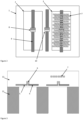
- Fig. 1 shows a schematic top-view of a double thermopile IR detector chip 1, with two membranes 2 and 3.
- the membranes are dielectric membranes and may comprise one or more layers of silicon dioxide and/or silicon nitride.
- a thermopile comprising one or more thermocouples connected in series, is embedded within each membrane to form two distinct thermopile IR detectors.
- Each thermocouple comprises of two dissimilar materials 4 and 5 which form a junction within the membrane while the other ends of the materials are outside the membrane where they are connected electrically to the adjacent thermocouple to form the cold junction.
- the thermocouple materials may comprise metal such as Aluminium, Tungsten, Titanium or combination of those, doped polysilicon (n or p type) or doped single crystal silicon (n or p type).
- a metal link 6 might be used to form the junctions between them.
- a plasmonic patterned layer 7 is also embedded within membrane 3, to provide the thermopile IR detector with tailored optical properties.
- the plasmonic patterned layer may be made of metal such as tungsten, aluminium, titanium, molybdenum, gold or platinum, silicides or polysilicon or single crystal silicon, and are periodically repeated in a lateral direction.
- the pattern may be made of dots or holes of circles, ellipses, rectangular structures, trapezoidal structures, or any other shape.
- the repeat pattern may be hexagonal or square.
- the structures may be in more than one layer, within or on the top surface of the membrane.
- Fig. 2 shows a schematic top-view of a double diode IR detector chip 1, with two membranes 2 and 3.
- the membranes are dielectric membranes and may comprise one or more layers of silicon dioxide and/or silicon nitride.
- a diode 8, and tracks 9, is embedded within each membrane to form to distinct diode IR detectors.
- the diodes may be made of polysilicon or of single crystal silicon.
- One or several diodes for enhanced sensitivity may be connected in series in the centre or in the proximity of the centre of the membrane.
- a plasmonic patterned layer 7 is also embedded within membrane 3, to provide the diode IR detector with tailored optical properties.
- the plasmonic patterned layer may be made of metal such as tungsten, aluminium, titanium, molybdenum, gold or platinum, silicides or polysilicon or single crystal silicon.
- the pattern may be made of circles, ellipses, rectangular structures, trapezoidal structures, or any other shape periodically repeated in a lateral direction.
- the repeat pattern may be hexagonal or square.
- the structures may be in more than one layer within or on the top surface of the membrane.
- a reference diode 10 that measures the substrate/case/ambient temperature is also placed outside the membrane areas.
- Fig. 3 shows the schematic cross-section of the double thermopile IR detector chip shown in Fig. 1 .
- the membranes 2 and 3 are supported on an etched substrate 11, and comprise dielectric layers 12 and may comprise one or more layers of silicon dioxide and/or silicon nitride.
- the thermopiles comprise p-doped silicon 4, and n-doped silicon 5, and a metal 6 is used to form a junction between them.
- the thermopile materials may comprise many other configurations, for example, n-doped silicon and metal, or p-doped silicon and metal.
- the silicon for the thermopiles may be polysilicon or single crystal silicon.
- a plasmonic patterned layer 7 is also embedded within membrane 3, to provide the thermopile IR detector with tailored optical properties.
- the substrate in this example is etched by Deep Reactive Ion Etching (DRIE) which results in vertical sidewalls.
- DRIE Deep Reactive Ion Etching
- Fig. 4 shows the schematic cross-section of the double diode IR detector chip shown in Fig. 2 .
- the membranes 2 and 3 are supported on an etched substrate 11, and comprise dielectric layers 12 and may comprise one or more layers of silicon dioxide and/or silicon nitride.
- the diodes 8 are made of single crystal silicon and contacted via metal tracks 9. Alternatively the diodes may be made of polysilicon.
- a plasmonic patterned layer 7, made of multiple metal layers, is also embedded within membrane 3, to provide the diode IR detector with tailored optical properties.
- a reference diode 10 that measures the substrate/case/ambient temperature is also placed outside the membrane areas.
- thermopile IR detector chip 1 with four membranes 2, 3, 13 and 14.
- the membranes are dielectric membranes and may comprise one or more layers of silicon dioxide and/or silicon nitride.
- a thermopile comprising one or more thermocouples connected in series, is embedded within each membrane to form four distinct thermopile IR detectors.
- Each thermocouple comprises two dissimilar materials 4 and 5 which form a junction within the membrane while the other ends of the materials are outside the membrane where they are connected electrically to the adjacent thermocouple to form the cold junction.
- the thermocouple materials may comprise metal such as Aluminium, Tungsten, Titanium or combination of those, doped polysilicon (n or p type) or doped single crystal silicon (n or p type).
- a metal link 6 might be used to form the junctions between them.
- a plasmonic patterned layer 7 is also embedded within membrane 3, to provide the thermopile IR detector with tailored optical properties.
- a plasmonic patterned layers 15 and 16 is also embedded within membrane 13 and 14, to provide the thermopile IR detectors with tailored optical properties different from each other and from the ones provided by layer 7.
- the patterned plasmonic layer may be identical in all the IR devices within the array. Alternately, the patterned plasmonic layer or layers may be different on each device, or may be the same across some devices, but different across others. The array may also have some devices with the same patterned plasmonic layer or layers and some without any patterned plasmonic layer.
- Fig. 6 shows a schematic top-view of a double diode IR detector chip 1, with a single membrane 2.
- the membrane is dielectric membrane and may comprise one or more layers of silicon dioxide and/or silicon nitride.
- Two diode 8, and tracks 9, are embedded within the membrane along with a separation 17 to form to diode IR detectors.
- the diodes may be made of polysilicon or of single crystal silicon.
- One or several diodes for enhanced sensitivity may be connected in series in the centre or in the proximity of the centre of the membrane.
- a plasmonic patterned layer 7 is also embedded within membrane 2, to provide only one of the diodes IR detectors with tailored optical properties.
- Fig. 7 shows the schematic cross-section of the double diode IR detector chip shown in Fig. 6 .
- the membranes 2 are supported on an etched substrate 11, and comprise dielectric layers 12 and may comprise one or more layers of silicon dioxide and/or silicon nitride.
- the diodes 8 are made of single crystal silicon and contacted via metal tracks 9. Alternatively, the diodes may be made of polysilicon.
- a plasmonic patterned layer 7, made of multiple metal layers, is also embedded within membrane 2, to provide only one of the diode IR detectors with tailored optical properties.
- Metal layers 17 are used to form the separation between the diodes. This separation area also acts as a heat sink.
- the separation 17, while made of metal in this figure, may also be made from single crystal silicon or polysilicon, or may comprise metal and polysilicon and/or single crystal silicon.
- the substrate in this example is etched by KOH resulting in sloping sidewalls.
- Fig. 8 shows the schematic cross-section of the double thermopile IR detector chip shown in Fig. 1 with circuitry on the same chip.
- the membranes 2 and 3 are supported on an etched substrate 11, and comprise dielectric layers 12 and may comprise one or more layers of silicon dioxide and/or silicon nitride.
- the thermopiles comprise p-doped silicon 4, and n-doped silicon 5, and a metal 6 is used to form a junction between them.
- the thermopile materials may comprise many other configurations, for example, n-doped silicon and metal or p-doped silicon and metal.
- the silicon for the thermopiles may be polysilicon or single crystal silicon.
- a plasmonic patterned layer 7 is also embedded within membrane 3, to provide the thermopile IR detector with tailored optical properties.
- the substrate in this example is etched by Deep Reactive Ion Etching (DRIE) which results in vertical sidewalls.
- DRIE Deep Reactive Ion Etching
- MOSFET 18 is shown, which comprises implant regions 19, a polysilicon gate and interconnect metal.
- Fig. 9 shows the schematic cross-section of the double thermopile IR detector chip shown in Fig. 1 with an IR emitter on the same chip.
- the membranes 2 and 3 are supported on an etched substrate 11, and comprise dielectric layers 12 and may comprise one or more layers of silicon dioxide and/or silicon nitride.
- the thermopiles comprise p-doped silicon 4, and n-doped silicon 5, and a metal 6 is used to form a junction between them.
- the thermopile materials may comprise many other configurations, for example, n-doped silicon and metal, or p-doped silicon and metal.
- the silicon for the thermopiles may be polysilicon or single crystal silicon.
- a plasmonic patterned layer 7 is also embedded within membrane 3, to provide the thermopile IR detector with tailored optical properties.
- the substrate in this example is etched by Deep Reactive Ion Etching (DRIE) which results in vertical sidewalls.
- DRIE Deep Reactive Ion Etching
- An IR emitter, in form of a microheater 20, is connected via tracks 21 and embedded within an additional membrane.
- a plasmonic patterned layer 22 is also embedded within the IR emitter membrane to provide the IR emitter with tailored optical properties.
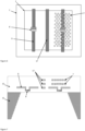
- Fig. 10 shows a schematic depiction of a double thermopile IR detector chip facing an IR emitter for filter-less carbon dioxide NDIR detection.
- the chips are both mounted on a package 23.
- the devices maybe packaged in a metal TO type package.
- the devices may also be packaged in a ceramic, metal or plastic SMD (surface mount device) package.
- the package may have one or more IR filters or windows, or a filter whose characteristics vary spatially.
- the package maybe hermetically or semi-hermetically sealed with air, dry air, argon, nitrogen, xenon or any other noble gas.
- the device may also be packaged in a vacuum.
- the device may also be packaged with a lens or a reflector.
- the package may also be a chip or wafer level package, formed for example, by wafer-bonding an etched wafer/chip on top, with the etched wafer/chip having a portion that is transparent to at least some wavelengths of IR.
- the device may also be packaged directly on a PCB, or be packaged in a flip-chip method. Even if in this example the NDIR system is for carbon dioxide detection, it may be used for detecting other gases (e.g. carbon monoxide, humidity, methane, etc.).
- Fig. 11 shows a schematic depiction of a double thermopile IR detector chip having an IR emitter fabricated on the same chip for filter-less carbon dioxide NDIR detection.
- the device maybe packaged in a metal transistor output (TO) type package.
- the device may also be packaged in a ceramic, metal or plastic SMD (surface mount device) package.
- the package may have one or more IR filters or windows, or a filter whose characteristics vary spatially.
- the package maybe hermetically or semi-hermetically sealed with air, dry air, argon, nitrogen, xenon or any other noble gas.
- the device may also be packaged in a vacuum.
- the device may also be packaged with a lens or a reflector.
- the package may also be a chip or wafer level package, formed for example, by wafer-bonding an etched wafer/chip on top, with the etched wafer/chip having a portion that is transparent to at least some wavelengths of IR.
- the device may also be packaged directly on a PCB, or be packaged in a flip-chip method. Even if in this example the NDIR system is for carbon dioxide detection, it may be used for detecting other gases (e.g. carbon monoxide, humidity, methane, etc.).
- the IR radiation is guided from the IR emitter to the IR detector via mirrors 24. Other methods for guiding the IR radiation from the IR emitter to the IR detector may be employed.
- Fig. 12 shows a schematic top-view of a double thermopile IR detector chip 1, with two membranes 2 and 3.
- the membranes are dielectric membranes and may comprise one or more layers of silicon dioxide and/or silicon nitride.
- a thermopile comprising one or more thermocouples connected in series, is embedded within each membrane to form two distinct thermopile IR detectors.
- Each thermocouple comprises two dissimilar materials 4 and 5 which form a junction within the membrane while the other ends of the materials are outside the membrane where they are connected electrically to the adjacent thermocouple to form the cold junction.
- the thermocouple materials may comprise metal such as Aluminium, Tungsten, Titanium or combination of those, doped polysilicon (n or p type) or doped single crystal silicon (n or p type).
- thermopile IR detector In the example that both the materials are polysilicon and/or single crystal silicon, a metal link 6 might be used to form the junctions between them.
- a plasmonic patterned layer 7 is also embedded within membrane 3, to provide the thermopile IR detector with tailored optical properties.
- a differential amplifier 25 and circuitry for signal processing 26 are co-integrated on the same chip to provide the double thermopile IR detector chip with a single output 27, thus facilitating the integration of the chip in a system and improving the chip performance by reducing parasitic components arising from the implementation of such circuitry on a separate chip or PCB.
- Fig. 13 shows the carbon dioxide detection capabilities of a chip similar to the one depicted in Fig. 12 in the NDIR configuration similar to the one depicted in Fig. 10 .
- Fig 14 illustrates an exemplary flow diagram outlining the manufacturing method of the IR detector array device.
Landscapes
- Physics & Mathematics (AREA)
- Engineering & Computer Science (AREA)
- Power Engineering (AREA)
- General Physics & Mathematics (AREA)
- Microelectronics & Electronic Packaging (AREA)
- Computer Hardware Design (AREA)
- Condensed Matter Physics & Semiconductors (AREA)
- Electromagnetism (AREA)
- Spectroscopy & Molecular Physics (AREA)
- Manufacturing & Machinery (AREA)
- Chemical & Material Sciences (AREA)
- Inorganic Chemistry (AREA)
- Photometry And Measurement Of Optical Pulse Characteristics (AREA)
- Investigating Or Analysing Materials By Optical Means (AREA)
Claims (14)
- Infrarot-(IR)-Detektor-Array-Vorrichtung (1), die Folgendes umfasst:ein Halbleitersubstrat (11), das einen geätzten Abschnitt umfasst;mindestens zwei dielektrische Membranen (2, 3), die auf dem Halbleitersubstrat (11) ausgebildet sind;ein Array von IR-Detektoren, das mindestens zwei IR-Detektoren umfasst, wobei das Array von IR-Detektoren auf den oder innerhalb der mindestens zwei dielektrischen Membranen (2, 3) ausgebildet ist; und wobei ein erster IR-Detektor des Arrays von IR-Detektoren auf oder innerhalb einer ersten dielektrischen Membran (2) ausgebildet ist und wobei ein zweiter IR-Detektor des Arrays von IR-Detektoren auf oder innerhalb einer zweiten dielektrischen Membran (3) ausgebildet ist; undmindestens eine strukturierte Schicht (7), die innerhalb oder auf mindestens einer der dielektrischen Membranen ausgebildet ist, um die IR-Absorption von mindestens einem der IR-Detektoren zu steuern, undwobei die mindestens eine strukturierte Schicht (7) lateral beabstandete Strukturen umfasst; undwobei sich die mindestens eine strukturierte Schicht (7) über einem der mindestens zwei IR-Detektoren befindet, so dass die mindestens eine strukturierte Schicht (7) mit einem der mindestens zwei IR-Detektoren assoziiert ist, unddie ferner Schaltungen (25, 26, 27) umfasst, die auf demselben Chip wie das Array von IR-Detektoren ausgebildet sind, wobei die Schaltungen analoge Schaltungen zur Verbesserung der spektralen Selektivität durch Verarbeiten der Ausgänge von jedem einzelnen IR-Detektor innerhalb des Arrays umfasst; undwobei die Schaltungen einen Differenzverstärker umfassen, um das Differenzsignal zwischen zwei IR-Detektoren zu bestimmen, um die Differenz in einer spektralen Antwort zu extrahieren.
- Vorrichtung nach Anspruch 1, wobei sich die mindestens eine strukturierte Schicht über allen IR-Detektoren innerhalb der dielektrischen Membranen befindet, so dass die mindestens eine strukturierte Schicht mit allen der mindestens zwei IR-Detektoren assoziiert ist; und/oderwobei die mindestens eine strukturierte Schicht mit den lateral beabstandeten Strukturen das gleiche Muster über mindestens einigen der IR-Detektoren hat; und/oderwobei die mindestens eine strukturierte Schicht mit den lateral beabstandeten Strukturen ein anderes Muster über mindestens einigen der IR-Detektoren hat.
- Vorrichtung nach Anspruch 1, wobei die mindestens eine strukturierte Schicht einen ersten Satz von lateral beabstandeten Strukturen über einem der IR-Detektoren und einen zweiten Satz von lateral beabstandeten Strukturen über einem anderen der IR-Detektoren umfasst, wobei der erste und der zweite Satz von lateral beabstandeten Strukturen das gleiche Muster haben; oder
wobei die mindestens eine strukturierte Schicht einen ersten Satz von lateral beabstandeten Strukturen (15) über einem der IR-Detektoren und einen zweiten Satz von lateral beabstandeten Strukturen (16) über einem anderen der IR-Detektoren umfasst, wobei der erste und der zweite Satz von lateral beabstandeten Strukturen (15, 16) ein anderes Muster haben. - Vorrichtung nach Anspruch 1, wobei jede lateral beabstandete Struktur ein Metall umfasst, das Gold oder Platin oder ein Metall auf CMOS-Basis wie Aluminium, Kupfer, Titan, Molybdän oder Wolfram umfasst; und/oderwobei die Strukturen periodisch in einer lateralen Richtung wiederholt werden und ein Wiederholungsmuster bilden; undwobei optional das Wiederholungsmuster eine hexagonale oder quadratische Form umfasst; und/oderwobei die Strukturen einen Kreis, eine Ellipse, ein Rechteck, ein Trapez oder eine Kombination verschiedener Formen oder ein Loch aus diesen Formen innerhalb einer Schicht umfassen, und/oderwobei die strukturierte Schicht ein kristallines Silizium oder Polysilizium umfasst.
- Vorrichtung nach Anspruch 1, wobei die IR-Detektoren eines oder mehrere von einer Thermosäule, einem Widerstand, einem Transistor und einer Diode umfassen, und/oderwobei jeder IR-Detektor eine Thermosäule umfasst, die ein oder mehrere jeweils in Reihe geschaltete Thermoelemente umfasst; undwobei optional jedes Thermoelement ferner einen ersten thermischen Übergang umfasst und mit benachbarten Thermoelementen verbunden ist, um einen zweiten thermischen Übergang zu bilden, wobei der erste thermische Übergang ein heißer Übergang ist und der zweite thermische Übergang ein kalter Übergang ist; undwobei sich der heiße Übergang optional innerhalb der dielektrischen Membran und der kalte Übergang außerhalb der dielektrischen Membran befindet.
- Vorrichtung nach Anspruch 1, wobei jeder IR-Detektor mindestens eine Diode (8) umfasst, wobei die mindestens eine Diode (8) ein Material umfasst, das Polysilizium oder einkristallines Silizium umfasst; unddie optional ferner eine Referenzdiode (10) umfasst, die sich außerhalb der dielektrischen Membranen befindet, um die Substrat- oder Umgebungstemperatur zu messen; oderwobei jeder IR-Detektor eine Thermosäule umfasst, in der der Seeback-Effekt und der Widerstandsänderungseffekt zum Bestimmen von IR-Strahlung verwendet werden, oderwobei jeder IR-Detektor eine Thermosäule umfasst, die mit einer Referenzdiode in der kalten Übergangsregion gekoppelt ist, um eine Schätzung der Temperatur des kalten Übergangs zu ermitteln, die zum Bestimmen einer absoluten Temperatur des heißen Übergangs verwendet wird.
- Vorrichtung nach Anspruch 1, die mit Schaltungen im selben Gehäuse ausgebildet ist.
- Vorrichtung nach Anspruch 1, wobei die Schaltungen eines von: einem Schalter, einem Multiplexer, einem Decoder, einem Filter, einem Verstärker, einem Analog-Digital-Wandler und/oder anderen Schaltungen umfassen, und/oderwobei die Schaltungen außerhalb des Bereichs der mindestens einen dielektrischen Membranfläche angeordnet sind; und/oderwobei die Schaltungen eines oder mehrere umfassen von:einem IR-Detektor;einem Multiplexer und Decoder, um jeden Detektor in dem Array zu adressieren;einem Temperatursensor zum Überwachen und Kompensieren der Umgebungstemperatur;einer Ansteuerungs- und Ausleseschaltung für den Temperatursensor; undeiner Ansteuerungs- und Ausleseschaltung für den IR-Detektor; und/oderdie ferner digitale Schnittstellen- und Verarbeitungsvorrichtungen (26) umfasst, die auf demselben Chip oder in demselben Gehäuse ausgebildet sind, um verbesserte Verarbeitung und spektrale Selektivität zu ermöglichen.
- Vorrichtung nach Anspruch 1, wobei das Substrat eines umfasst von:Silizium;Silizium auf Isolator;Siliziumkarbid,Galliumarsenid,Galliumnitrid; und/odereine Kombination aus Siliziumkarbid, Galliumarsenid, Galliumnitrid und Silizium; und/oderwobei die Vorrichtung unter Verwendung eines CMOS-verwendbaren Metalls hergestellt ist, ausgewählt aus einer Gruppe, die Wolfram, Aluminium, Titan und Molybdän umfasst; oderwobei die IR-Detektoren unter Verwendung eines CMOS-verwendbaren Materials gebildet werden, das aus einer Gruppe ausgewählt ist, die Silizium, Polysilizium und Silizide umfasst; oderwobei die Vorrichtung unter Verwendung eines nicht CMOS-kompatiblen Materials hergestellt ist.
- Vorrichtung nach Anspruch 1, die ferner einen IR-Emitter (20) umfasst, und wobei der IR-Emitter (20) und das IR-Detektorarray auf einem einzigen Chip hergestellt sind; undwobei der IR-Emitter (20) optional auf oder innerhalb einer separaten Membran ausgebildet ist; und/oderwobei der IR-Emitter eine Heizung umfasst, die eines oder mehrere von Wolfram, Aluminium, Kupfer, Polysilizium, einkristallinem Silizium, Titan, Platin und Gold umfasst; und/oderwobei der IR-Emitter eine oder mehrere plasmonisch strukturierte Schichten (22) innerhalb oder auf einer Seite der dielektrischen Membran umfasst.
- NDIR-(Non-Dispersives Infra-Red)-Sensorsystem oder spektroskopisches Sensorsystem, das die IR-Detektor-Array-Vorrichtung nach Anspruch 1 und einen IR-Emitter umfasst.
- Sensorsystem nach Anspruch 11, wobei die IR-Detektor-Array-Vorrichtung und der IR-Emitter auf demselben Chip ausgebildet sind; oderwobei die IR-Detektor-Array-Vorrichtung und der IR-Emitter auf einem anderen Chip ausgebildet sind, oder der IR-Emitter eine Mikrolampe oder einen diodenbasierten IR-Emitter umfasst; und/oderdas ferner mindestens ein IR-Filter umfasst; und/oderdas ferner eine reflektierende Vorrichtung umfasst.
- Sensorsystem nach Anspruch 11, wobei die mindestens eine mit jedem IR-Detektor assoziierte strukturierte Schicht so konfiguriert ist, dass sie mindestens eine Wellenlänge erzeugt; undwobei das Sensorsystem optional zum Subtrahieren des Ausgangssignals von einem der IR-Detektoren von dem Ausgangssignal von dem anderen der IR-Detektoren konfiguriert ist, um mindestens eine IR-Absorptionswellenlänge bereitzustellen; undwobei das Sensorsystem optional zum Identifizieren eines Gases aus dem von den IR-Detektoren empfangenen Signal konfiguriert ist; und/oderwobei das Sensorsystem zum Bestimmen der Gaskonzentration aus dem von dem Detektorarray empfangenen Signal konfiguriert ist; undwobei das Sensorsystem optional so konfiguriert ist, dass der Ausgang von jedem IR-Detektor gruppiert oder verarbeitet wird, um die Chrakteristiken des Gases zu extrahieren.
- Verfahren zur Herstellung einer Infrarot-(IR)-Detektor-Array-Vorrichtung (1), wobei das Verfahren Folgendes umfasst:Bilden eines Halbleitersubstrats (11);Absetzen einer oder mehrerer Schichten aus Polysilizium und/oder Metallen und dielektrischen Schichten (12), um ein Array von IR-Detektoren und mindestens eine strukturierte Schicht (7) zu bilden;Bulk-Ätzen des Halbleitersubstrats (11) zur Bildung von mindestens zwei dielektrischen Membranen (2, 3);wobei ein erster IR-Detektor des Arrays von IR-Detektoren auf oder innerhalb einer ersten dielektrischen Membran (2) ausgebildet ist, und wobei ein zweiter IR-Detektor auf oder innerhalb einer zweiten dielektrischen Membran (3) ausgebildet ist;wobei die mindestens eine strukturierte Schicht (7) innerhalb oder auf mindestens einer der dielektrischen Membranen (2, 3) ausgebildet ist, um die IR-Absorption von mindestens einem der IR-Detektoren zu steuern, und wobei die mindestens eine strukturierte Schicht (7) lateral beabstandete Strukturen umfasst; und wobei sich die mindestens eine strukturierte Schicht (7) über einem der IR-Detektoren befindet, so dass die mindestens eine strukturierte Schicht (7) mit einem der mindestens zwei IR-Detektoren assoziiert ist; undAusbilden von Schaltungen (25, 26, 27) auf demselben Chip mit dem Array von IR-Detektoren, wobei die Schaltungen analoge Schaltungen umfassen, um die spektrale Selektivität durch Verarbeiten der Ausgänge von jedem einzelnen IR-Detektor innerhalb des Arrays zu verbessern, und wobei die Schaltungen einen Differenzverstärker umfassen, um das Differenzsignal zwischen zwei IR-Detektoren zu bestimmen, um die Differenz in einer spektralen Antwort zu extrahieren.
Applications Claiming Priority (2)
| Application Number | Priority Date | Filing Date | Title |
|---|---|---|---|
| US15/009,300 US10551246B2 (en) | 2016-01-28 | 2016-01-28 | IR detector array device |
| PCT/GB2017/050177 WO2017129966A1 (en) | 2016-01-28 | 2017-01-24 | An ir detector array device |
Publications (2)
| Publication Number | Publication Date |
|---|---|
| EP3408629A1 EP3408629A1 (de) | 2018-12-05 |
| EP3408629B1 true EP3408629B1 (de) | 2024-03-20 |
Family
ID=57909802
Family Applications (1)
| Application Number | Title | Priority Date | Filing Date |
|---|---|---|---|
| EP17701922.1A Active EP3408629B1 (de) | 2016-01-28 | 2017-01-24 | Ir-detektor-array-vorrichtung |
Country Status (4)
| Country | Link |
|---|---|
| US (1) | US10551246B2 (de) |
| EP (1) | EP3408629B1 (de) |
| CN (1) | CN108885137A (de) |
| WO (1) | WO2017129966A1 (de) |
Families Citing this family (10)
| Publication number | Priority date | Publication date | Assignee | Title |
|---|---|---|---|---|
| WO2018079788A1 (ja) * | 2016-10-31 | 2018-05-03 | 京セラ株式会社 | プローブカード用基板、プローブカード、および検査装置 |
| US10436646B2 (en) * | 2018-02-28 | 2019-10-08 | Ams Sensors Uk Limited | IR detector arrays |
| CN114761773A (zh) * | 2019-05-21 | 2022-07-15 | 触控解决方案股份有限公司 | 芯片级封装中的组合式近红外和中红外传感器 |
| CN114788020A (zh) * | 2019-12-20 | 2022-07-22 | ams国际有限公司 | Cmos兼容的近红外传感器系统 |
| CN111060466B (zh) * | 2019-12-30 | 2023-01-13 | 暨南大学 | 一种便携式光学气体传感器 |
| DE102020100244A1 (de) | 2020-01-08 | 2021-07-08 | X-FAB Global Services GmbH | Verfahren zur Herstellung eines Membran-Bauelements und ein Membran-Bauelement |
| CN113655535B (zh) * | 2021-07-05 | 2024-06-14 | 中国电子科技集团公司第十一研究所 | 引出组件及红外探测器 |
| CN113566982B (zh) * | 2021-07-12 | 2022-05-24 | 北京北方高业科技有限公司 | 一种微桥结构红外探测器 |
| US11808633B2 (en) * | 2021-08-16 | 2023-11-07 | Oriental System Technology Inc. | Infrared thermopile sensor |
| TWI816360B (zh) * | 2022-04-11 | 2023-09-21 | 國立高雄科技大學 | 非制冷型紅外線感測器 |
Citations (1)
| Publication number | Priority date | Publication date | Assignee | Title |
|---|---|---|---|---|
| EP2847561A1 (de) * | 2012-05-08 | 2015-03-18 | Cambridge CMOS Sensors Limited | Ir-thermosäulen-detektor |
Family Cites Families (14)
| Publication number | Priority date | Publication date | Assignee | Title |
|---|---|---|---|---|
| JPS57113332A (en) | 1980-12-30 | 1982-07-14 | Horiba Ltd | Compensating thermopile detector |
| US5081998A (en) * | 1989-09-01 | 1992-01-21 | Critikon, Inc. | Optically stabilized infrared energy detector |
| US5624709A (en) * | 1995-06-07 | 1997-04-29 | Santa Barbara Research Center | High resolution differential spectrometry system |
| EP0863389B1 (de) * | 1997-02-28 | 2003-09-17 | EM Microelectronic-Marin SA | Thermoelektrischer Fühler |
| US6239434B1 (en) * | 1999-02-08 | 2001-05-29 | General Electric Company | Solid state optical spectrometer for combustion flame temperature measurement |
| US7842922B2 (en) * | 2005-05-17 | 2010-11-30 | Heimann Sensor Gmbh | Thermopile infrared sensor array |
| US7785002B2 (en) | 2006-12-05 | 2010-08-31 | Delphi Technologies, Inc. | P-N junction based thermal detector |
| US8859303B2 (en) | 2010-01-21 | 2014-10-14 | Cambridge Cmos Sensors Ltd. | IR emitter and NDIR sensor |
| US9214604B2 (en) | 2010-01-21 | 2015-12-15 | Cambridge Cmos Sensors Limited | Plasmonic IR devices |
| KR102132359B1 (ko) * | 2012-05-08 | 2020-07-10 | 사이오센스 비.브이. | 적외선 에미터 및 비분산 적외선 센서 |
| DE102012220207A1 (de) * | 2012-11-07 | 2014-05-08 | Robert Bosch Gmbh | Bildpixelvorrichtung zum Erfassen von elektromagnetischer Strahlung, Sensorarray zum Erfassen von elektromagnetischer Strahlung und Verfahren zum Erfassen von elektromagnetischer Strahlung mittels einer Bildpixelvorrichtung |
| WO2015017703A2 (en) * | 2013-08-01 | 2015-02-05 | The Regents Of The University Of California | Pyroelectric aluminum nitride mems infrared sensor with selective wavelength infrared absorber |
| CN104535197A (zh) * | 2014-12-29 | 2015-04-22 | 杭州士兰集成电路有限公司 | 热电堆红外探测器及其制作方法 |
| US9909926B2 (en) * | 2016-05-31 | 2018-03-06 | Ams Sensors Uk Limited | Chemical sensor |
-
2016
- 2016-01-28 US US15/009,300 patent/US10551246B2/en active Active
-
2017
- 2017-01-24 CN CN201780008612.7A patent/CN108885137A/zh active Pending
- 2017-01-24 WO PCT/GB2017/050177 patent/WO2017129966A1/en active Application Filing
- 2017-01-24 EP EP17701922.1A patent/EP3408629B1/de active Active
Patent Citations (1)
| Publication number | Priority date | Publication date | Assignee | Title |
|---|---|---|---|---|
| EP2847561A1 (de) * | 2012-05-08 | 2015-03-18 | Cambridge CMOS Sensors Limited | Ir-thermosäulen-detektor |
Also Published As
| Publication number | Publication date |
|---|---|
| EP3408629A1 (de) | 2018-12-05 |
| US20170219434A1 (en) | 2017-08-03 |
| CN108885137A (zh) | 2018-11-23 |
| US10551246B2 (en) | 2020-02-04 |
| WO2017129966A1 (en) | 2017-08-03 |
Similar Documents
| Publication | Publication Date | Title |
|---|---|---|
| EP3408629B1 (de) | Ir-detektor-array-vorrichtung | |
| Xu et al. | MEMS-based thermoelectric infrared sensors: A review | |
| US20200370963A1 (en) | Thermopile infrared individual sensor for measuring temperature or detecting gas | |
| US8304850B2 (en) | Integrated infrared sensors with optical elements, and methods | |
| EP3408630B1 (de) | Ir-detektor-array-vorrichtung | |
| KR102108569B1 (ko) | 적외선 써모파일 검출기 | |
| Li et al. | A front-side microfabricated tiny-size thermopile infrared detector with high sensitivity and fast response | |
| JP2019504298A (ja) | ウェハレベルパッケージ内の熱赤外線センサアレイ | |
| CN102244190B (zh) | 一种热电堆红外探测器 | |
| EP4354102A2 (de) | Infrarotvorrichtung | |
| US8465202B2 (en) | Microstructured sensor for the detection of IR radiation | |
| EP1464933A2 (de) | Vorrichtung zum Detektieren von Infrarotstrahlung | |
| JP3580126B2 (ja) | 赤外線センサ | |
| US10436646B2 (en) | IR detector arrays | |
| US8952480B2 (en) | Electronic device including thermal sensor and peltier cooler and related methods | |
| JP2010256189A (ja) | 赤外線センサ | |
| JP2018179860A (ja) | 赤外線検出装置の製造方法 |
Legal Events
| Date | Code | Title | Description |
|---|---|---|---|
| STAA | Information on the status of an ep patent application or granted ep patent |
Free format text: STATUS: UNKNOWN |
|
| STAA | Information on the status of an ep patent application or granted ep patent |
Free format text: STATUS: THE INTERNATIONAL PUBLICATION HAS BEEN MADE |
|
| PUAI | Public reference made under article 153(3) epc to a published international application that has entered the european phase |
Free format text: ORIGINAL CODE: 0009012 |
|
| STAA | Information on the status of an ep patent application or granted ep patent |
Free format text: STATUS: REQUEST FOR EXAMINATION WAS MADE |
|
| 17P | Request for examination filed |
Effective date: 20180706 |
|
| AK | Designated contracting states |
Kind code of ref document: A1 Designated state(s): AL AT BE BG CH CY CZ DE DK EE ES FI FR GB GR HR HU IE IS IT LI LT LU LV MC MK MT NL NO PL PT RO RS SE SI SK SM TR |
|
| AX | Request for extension of the european patent |
Extension state: BA ME |
|
| RIN1 | Information on inventor provided before grant (corrected) |
Inventor name: HOPPER, RICHARD HENRY Inventor name: ALI, SYED ZEESHAN Inventor name: UDREA, FLORIN Inventor name: DE LUCA, ANDREA Inventor name: GARDNER, JULIAN |
|
| STAA | Information on the status of an ep patent application or granted ep patent |
Free format text: STATUS: REQUEST FOR EXAMINATION WAS MADE |
|
| DAV | Request for validation of the european patent (deleted) | ||
| DAX | Request for extension of the european patent (deleted) | ||
| STAA | Information on the status of an ep patent application or granted ep patent |
Free format text: STATUS: EXAMINATION IS IN PROGRESS |
|
| 17Q | First examination report despatched |
Effective date: 20220207 |
|
| RIC1 | Information provided on ipc code assigned before grant |
Ipc: H01L 27/144 20060101ALI20230809BHEP Ipc: H10N 19/00 20230101ALI20230809BHEP Ipc: H01L 27/146 20060101ALI20230809BHEP Ipc: G01J 3/42 20060101ALI20230809BHEP Ipc: G01J 3/28 20060101ALI20230809BHEP Ipc: G01J 5/02 20060101ALI20230809BHEP Ipc: G01J 5/20 20060101ALI20230809BHEP Ipc: G01J 5/12 20060101ALI20230809BHEP Ipc: G01J 5/08 20060101AFI20230809BHEP |
|
| GRAP | Despatch of communication of intention to grant a patent |
Free format text: ORIGINAL CODE: EPIDOSNIGR1 |
|
| STAA | Information on the status of an ep patent application or granted ep patent |
Free format text: STATUS: GRANT OF PATENT IS INTENDED |
|
| INTG | Intention to grant announced |
Effective date: 20231002 |
|
| GRAS | Grant fee paid |
Free format text: ORIGINAL CODE: EPIDOSNIGR3 |
|
| GRAA | (expected) grant |
Free format text: ORIGINAL CODE: 0009210 |
|
| STAA | Information on the status of an ep patent application or granted ep patent |
Free format text: STATUS: THE PATENT HAS BEEN GRANTED |
|
| AK | Designated contracting states |
Kind code of ref document: B1 Designated state(s): AL AT BE BG CH CY CZ DE DK EE ES FI FR GB GR HR HU IE IS IT LI LT LU LV MC MK MT NL NO PL PT RO RS SE SI SK SM TR |
|
| REG | Reference to a national code |
Ref country code: GB Ref legal event code: FG4D |
|
| REG | Reference to a national code |
Ref country code: CH Ref legal event code: EP |
|
| REG | Reference to a national code |
Ref country code: IE Ref legal event code: FG4D |
|
| REG | Reference to a national code |
Ref country code: DE Ref legal event code: R096 Ref document number: 602017080168 Country of ref document: DE |
|
| PG25 | Lapsed in a contracting state [announced via postgrant information from national office to epo] |
Ref country code: LT Free format text: LAPSE BECAUSE OF FAILURE TO SUBMIT A TRANSLATION OF THE DESCRIPTION OR TO PAY THE FEE WITHIN THE PRESCRIBED TIME-LIMIT Effective date: 20240320 |
|
| REG | Reference to a national code |
Ref country code: LT Ref legal event code: MG9D |
|
| PG25 | Lapsed in a contracting state [announced via postgrant information from national office to epo] |
Ref country code: GR Free format text: LAPSE BECAUSE OF FAILURE TO SUBMIT A TRANSLATION OF THE DESCRIPTION OR TO PAY THE FEE WITHIN THE PRESCRIBED TIME-LIMIT Effective date: 20240621 |
|
| PG25 | Lapsed in a contracting state [announced via postgrant information from national office to epo] |
Ref country code: RS Free format text: LAPSE BECAUSE OF FAILURE TO SUBMIT A TRANSLATION OF THE DESCRIPTION OR TO PAY THE FEE WITHIN THE PRESCRIBED TIME-LIMIT Effective date: 20240620 Ref country code: HR Free format text: LAPSE BECAUSE OF FAILURE TO SUBMIT A TRANSLATION OF THE DESCRIPTION OR TO PAY THE FEE WITHIN THE PRESCRIBED TIME-LIMIT Effective date: 20240320 |
|
| REG | Reference to a national code |
Ref country code: NL Ref legal event code: MP Effective date: 20240320 |
|
| PG25 | Lapsed in a contracting state [announced via postgrant information from national office to epo] |
Ref country code: RS Free format text: LAPSE BECAUSE OF FAILURE TO SUBMIT A TRANSLATION OF THE DESCRIPTION OR TO PAY THE FEE WITHIN THE PRESCRIBED TIME-LIMIT Effective date: 20240620 Ref country code: NO Free format text: LAPSE BECAUSE OF FAILURE TO SUBMIT A TRANSLATION OF THE DESCRIPTION OR TO PAY THE FEE WITHIN THE PRESCRIBED TIME-LIMIT Effective date: 20240620 Ref country code: LT Free format text: LAPSE BECAUSE OF FAILURE TO SUBMIT A TRANSLATION OF THE DESCRIPTION OR TO PAY THE FEE WITHIN THE PRESCRIBED TIME-LIMIT Effective date: 20240320 Ref country code: HR Free format text: LAPSE BECAUSE OF FAILURE TO SUBMIT A TRANSLATION OF THE DESCRIPTION OR TO PAY THE FEE WITHIN THE PRESCRIBED TIME-LIMIT Effective date: 20240320 Ref country code: GR Free format text: LAPSE BECAUSE OF FAILURE TO SUBMIT A TRANSLATION OF THE DESCRIPTION OR TO PAY THE FEE WITHIN THE PRESCRIBED TIME-LIMIT Effective date: 20240621 Ref country code: FI Free format text: LAPSE BECAUSE OF FAILURE TO SUBMIT A TRANSLATION OF THE DESCRIPTION OR TO PAY THE FEE WITHIN THE PRESCRIBED TIME-LIMIT Effective date: 20240320 Ref country code: BG Free format text: LAPSE BECAUSE OF FAILURE TO SUBMIT A TRANSLATION OF THE DESCRIPTION OR TO PAY THE FEE WITHIN THE PRESCRIBED TIME-LIMIT Effective date: 20240320 |
|
| REG | Reference to a national code |
Ref country code: AT Ref legal event code: MK05 Ref document number: 1668212 Country of ref document: AT Kind code of ref document: T Effective date: 20240320 |
|
| PG25 | Lapsed in a contracting state [announced via postgrant information from national office to epo] |
Ref country code: SE Free format text: LAPSE BECAUSE OF FAILURE TO SUBMIT A TRANSLATION OF THE DESCRIPTION OR TO PAY THE FEE WITHIN THE PRESCRIBED TIME-LIMIT Effective date: 20240320 Ref country code: LV Free format text: LAPSE BECAUSE OF FAILURE TO SUBMIT A TRANSLATION OF THE DESCRIPTION OR TO PAY THE FEE WITHIN THE PRESCRIBED TIME-LIMIT Effective date: 20240320 |
|
| PG25 | Lapsed in a contracting state [announced via postgrant information from national office to epo] |
Ref country code: NL Free format text: LAPSE BECAUSE OF FAILURE TO SUBMIT A TRANSLATION OF THE DESCRIPTION OR TO PAY THE FEE WITHIN THE PRESCRIBED TIME-LIMIT Effective date: 20240320 |