EP3407102A1 - Filtre multispectral d'espacement mixte - Google Patents
Filtre multispectral d'espacement mixte Download PDFInfo
- Publication number
- EP3407102A1 EP3407102A1 EP18170858.7A EP18170858A EP3407102A1 EP 3407102 A1 EP3407102 A1 EP 3407102A1 EP 18170858 A EP18170858 A EP 18170858A EP 3407102 A1 EP3407102 A1 EP 3407102A1
- Authority
- EP
- European Patent Office
- Prior art keywords
- approximately
- layers
- refractive index
- layer
- optical filter
- Prior art date
- Legal status (The legal status is an assumption and is not a legal conclusion. Google has not performed a legal analysis and makes no representation as to the accuracy of the status listed.)
- Granted
Links
- 125000006850 spacer group Chemical group 0.000 title claims abstract description 81
- 230000003287 optical effect Effects 0.000 claims abstract description 72
- 239000000463 material Substances 0.000 claims abstract description 54
- VYPSYNLAJGMNEJ-UHFFFAOYSA-N Silicium dioxide Chemical compound O=[Si]=O VYPSYNLAJGMNEJ-UHFFFAOYSA-N 0.000 claims description 64
- 239000000377 silicon dioxide Substances 0.000 claims description 32
- 235000012239 silicon dioxide Nutrition 0.000 claims description 28
- OBOYOXRQUWVUFU-UHFFFAOYSA-N [O-2].[Ti+4].[Nb+5] Chemical compound [O-2].[Ti+4].[Nb+5] OBOYOXRQUWVUFU-UHFFFAOYSA-N 0.000 claims description 19
- 238000000926 separation method Methods 0.000 claims description 11
- 230000003595 spectral effect Effects 0.000 claims description 9
- 239000000758 substrate Substances 0.000 claims description 9
- ZKATWMILCYLAPD-UHFFFAOYSA-N niobium pentoxide Inorganic materials O=[Nb](=O)O[Nb](=O)=O ZKATWMILCYLAPD-UHFFFAOYSA-N 0.000 claims description 6
- URLJKFSTXLNXLG-UHFFFAOYSA-N niobium(5+);oxygen(2-) Chemical compound [O-2].[O-2].[O-2].[O-2].[O-2].[Nb+5].[Nb+5] URLJKFSTXLNXLG-UHFFFAOYSA-N 0.000 claims description 6
- TWNQGVIAIRXVLR-UHFFFAOYSA-N oxo(oxoalumanyloxy)alumane Chemical compound O=[Al]O[Al]=O TWNQGVIAIRXVLR-UHFFFAOYSA-N 0.000 claims description 6
- SIWVEOZUMHYXCS-UHFFFAOYSA-N oxo(oxoyttriooxy)yttrium Chemical compound O=[Y]O[Y]=O SIWVEOZUMHYXCS-UHFFFAOYSA-N 0.000 claims description 6
- BPUBBGLMJRNUCC-UHFFFAOYSA-N oxygen(2-);tantalum(5+) Chemical compound [O-2].[O-2].[O-2].[O-2].[O-2].[Ta+5].[Ta+5] BPUBBGLMJRNUCC-UHFFFAOYSA-N 0.000 claims description 6
- RVTZCBVAJQQJTK-UHFFFAOYSA-N oxygen(2-);zirconium(4+) Chemical compound [O-2].[O-2].[Zr+4] RVTZCBVAJQQJTK-UHFFFAOYSA-N 0.000 claims description 6
- PBCFLUZVCVVTBY-UHFFFAOYSA-N tantalum pentoxide Inorganic materials O=[Ta](=O)O[Ta](=O)=O PBCFLUZVCVVTBY-UHFFFAOYSA-N 0.000 claims description 6
- 229910001928 zirconium oxide Inorganic materials 0.000 claims description 6
- 229910052751 metal Inorganic materials 0.000 claims description 5
- 239000002184 metal Substances 0.000 claims description 5
- KRHYYFGTRYWZRS-UHFFFAOYSA-M Fluoride anion Chemical compound [F-] KRHYYFGTRYWZRS-UHFFFAOYSA-M 0.000 claims description 3
- UCKMPCXJQFINFW-UHFFFAOYSA-N Sulphide Chemical compound [S-2] UCKMPCXJQFINFW-UHFFFAOYSA-N 0.000 claims description 3
- GWEVSGVZZGPLCZ-UHFFFAOYSA-N Titan oxide Chemical compound O=[Ti]=O GWEVSGVZZGPLCZ-UHFFFAOYSA-N 0.000 claims description 3
- CJNBYAVZURUTKZ-UHFFFAOYSA-N hafnium(iv) oxide Chemical compound O=[Hf]=O CJNBYAVZURUTKZ-UHFFFAOYSA-N 0.000 claims description 3
- 150000004767 nitrides Chemical class 0.000 claims description 3
- 150000003346 selenoethers Chemical class 0.000 claims description 3
- 239000010410 layer Substances 0.000 description 204
- 150000003376 silicon Chemical class 0.000 description 68
- 238000010586 diagram Methods 0.000 description 12
- 230000008859 change Effects 0.000 description 10
- 238000000034 method Methods 0.000 description 9
- 239000000203 mixture Substances 0.000 description 9
- 230000004044 response Effects 0.000 description 8
- 230000003647 oxidation Effects 0.000 description 7
- 238000007254 oxidation reaction Methods 0.000 description 7
- 230000008569 process Effects 0.000 description 7
- 239000011248 coating agent Substances 0.000 description 6
- 238000000576 coating method Methods 0.000 description 6
- 238000002834 transmittance Methods 0.000 description 5
- 230000015556 catabolic process Effects 0.000 description 4
- 238000006731 degradation reaction Methods 0.000 description 4
- 238000004519 manufacturing process Methods 0.000 description 4
- 238000004140 cleaning Methods 0.000 description 3
- 239000006185 dispersion Substances 0.000 description 3
- 238000005516 engineering process Methods 0.000 description 3
- 238000000059 patterning Methods 0.000 description 3
- 239000011241 protective layer Substances 0.000 description 3
- 230000009467 reduction Effects 0.000 description 3
- PFNQVRZLDWYSCW-UHFFFAOYSA-N (fluoren-9-ylideneamino) n-naphthalen-1-ylcarbamate Chemical compound C12=CC=CC=C2C2=CC=CC=C2C1=NOC(=O)NC1=CC=CC2=CC=CC=C12 PFNQVRZLDWYSCW-UHFFFAOYSA-N 0.000 description 2
- 229910052581 Si3N4 Inorganic materials 0.000 description 2
- 239000005083 Zinc sulfide Substances 0.000 description 2
- 239000000654 additive Substances 0.000 description 2
- 230000000996 additive effect Effects 0.000 description 2
- 230000001419 dependent effect Effects 0.000 description 2
- 238000013461 design Methods 0.000 description 2
- 230000007613 environmental effect Effects 0.000 description 2
- 230000006872 improvement Effects 0.000 description 2
- ORUIBWPALBXDOA-UHFFFAOYSA-L magnesium fluoride Chemical compound [F-].[F-].[Mg+2] ORUIBWPALBXDOA-UHFFFAOYSA-L 0.000 description 2
- 229910001635 magnesium fluoride Inorganic materials 0.000 description 2
- HQVNEWCFYHHQES-UHFFFAOYSA-N silicon nitride Chemical compound N12[Si]34N5[Si]62N3[Si]51N64 HQVNEWCFYHHQES-UHFFFAOYSA-N 0.000 description 2
- 239000000126 substance Substances 0.000 description 2
- 229910052984 zinc sulfide Inorganic materials 0.000 description 2
- XUIMIQQOPSSXEZ-UHFFFAOYSA-N Silicon Chemical group [Si] XUIMIQQOPSSXEZ-UHFFFAOYSA-N 0.000 description 1
- 230000004075 alteration Effects 0.000 description 1
- 230000000295 complement effect Effects 0.000 description 1
- 230000008021 deposition Effects 0.000 description 1
- 238000005137 deposition process Methods 0.000 description 1
- 238000005259 measurement Methods 0.000 description 1
- 238000012986 modification Methods 0.000 description 1
- 230000004048 modification Effects 0.000 description 1
- 230000010363 phase shift Effects 0.000 description 1
- 239000004065 semiconductor Substances 0.000 description 1
- LIVNPJMFVYWSIS-UHFFFAOYSA-N silicon monoxide Chemical compound [Si-]#[O+] LIVNPJMFVYWSIS-UHFFFAOYSA-N 0.000 description 1
- 239000002210 silicon-based material Substances 0.000 description 1
- 229910052709 silver Inorganic materials 0.000 description 1
- 239000004332 silver Substances 0.000 description 1
- 238000012360 testing method Methods 0.000 description 1
- DRDVZXDWVBGGMH-UHFFFAOYSA-N zinc;sulfide Chemical compound [S-2].[Zn+2] DRDVZXDWVBGGMH-UHFFFAOYSA-N 0.000 description 1
Images


Classifications
-
- G—PHYSICS
- G02—OPTICS
- G02B—OPTICAL ELEMENTS, SYSTEMS OR APPARATUS
- G02B5/00—Optical elements other than lenses
- G02B5/20—Filters
- G02B5/201—Filters in the form of arrays
-
- G—PHYSICS
- G02—OPTICS
- G02B—OPTICAL ELEMENTS, SYSTEMS OR APPARATUS
- G02B5/00—Optical elements other than lenses
- G02B5/20—Filters
- G02B5/207—Filters comprising semiconducting materials
-
- G—PHYSICS
- G02—OPTICS
- G02B—OPTICAL ELEMENTS, SYSTEMS OR APPARATUS
- G02B5/00—Optical elements other than lenses
- G02B5/20—Filters
- G02B5/28—Interference filters
-
- G—PHYSICS
- G02—OPTICS
- G02B—OPTICAL ELEMENTS, SYSTEMS OR APPARATUS
- G02B5/00—Optical elements other than lenses
- G02B5/20—Filters
- G02B5/28—Interference filters
- G02B5/281—Interference filters designed for the infrared light
-
- G—PHYSICS
- G02—OPTICS
- G02B—OPTICAL ELEMENTS, SYSTEMS OR APPARATUS
- G02B5/00—Optical elements other than lenses
- G02B5/20—Filters
- G02B5/28—Interference filters
- G02B5/285—Interference filters comprising deposited thin solid films
- G02B5/288—Interference filters comprising deposited thin solid films comprising at least one thin film resonant cavity, e.g. in bandpass filters
Definitions
- a multispectral sensor device may be utilized to capture information.
- the multispectral sensor device may capture information relating to a set of electromagnetic frequencies.
- the multispectral sensor device may include a set of sensor elements (e.g., optical sensors, spectral sensors, and/or image sensors) that capture the information.
- an array of sensor elements may be utilized to capture information relating to multiple frequencies.
- a particular sensor element, of the sensor element array may be associated with a filter that restricts a range of frequencies that are directed toward the particular sensor element.
- an optical filter may include a first mirror, a second mirror, and a spacer layer structure disposed between the first mirror and the second mirror.
- the spacer layer structure may include a first set of layers. Each layer, of the first set of layers, may be a first material associated with a first refractive index and a thickness that is greater than a layer thickness threshold.
- the spacer layer structure may include a second set of layers. Each layer, of the second set of layers, may be a second material associated with a second refractive index. Each layer, of the second set of, may be selected to replace a corresponding layer of the first material. The corresponding layer may be associated with a thickness that is less than the layer thickness threshold.
- the first material may be hydrogenated silicon.
- the first refractive index may be, at approximately 800 nanometers (nm), greater than at least one of: a 2.0 refractive index, a 2.5 refractive index, a 3.0 refractive index, a 3.5 refractive index, a 3.6 refractive index, or a 3.8 refractive index.
- the first material may be an oxidizable material.
- the second material may include an oxide material
- the oxide material may include at least one of: a niobium titanium oxide (NbTiOx), a silicon dioxide SiO 2 ), an aluminum oxide (Al 2 O 3 ), a titanium dioxide (TiO 2 ), a niobium pentoxide (Nb 2 O 5 ), a tantalum pentoxide (Ta 2 O 5 ), a zirconium oxide (ZrO 2 ), an yttrium oxide (Y 2 O 3 ), a hafnium dioxide (HfO 2 ), or a combination thereof.
- the second material may include at least one of: a nitride material, a fluoride material, a sulfide material, or a selenide material.
- the second refractive index may be less than the first refractive index.
- a thickness of a layer, of the second set of layers, may be selected based on the second refractive index.
- the second set of layers may form a plurality of channels each associated with a channel separation of less than a threshold channel separation.
- the threshold channel separation may be one of: approximately 30 nanometers (nm), approximately 15 nm, approximately 10 nm, approximately 7 nm, approximately 6 nm, or approximately 5 nm.
- the layer thickness threshold may be one of: approximately 10 nm, approximately 5 nm, approximately 2.5 nm, approximately 2 nm, approximately 1.5 nm, approximately 1 nm, or approximately 0.75 nm.
- the first mirror and the second mirror may each include one of: a metal mirror, or a dielectric mirror.
- a multispectral filter may include a first mirror deposited on a substrate associated with a set of sensor elements and to partially reflect light from a light source.
- the multispectral filter may include a second mirror to partially reflect light from the light source.
- the multispectral filter may include a spacer disposed between the first mirror and the second mirror and including a plurality of layers associated with a plurality of channels corresponding to the set of sensor elements.
- a first one or more layers, of the plurality of layers may be hydrogenated silicon with a first refractive index.
- Each of the first one or more layers may be associated with a thickness greater than a layer thickness threshold.
- a second one or more layers, of the plurality of layers may be associated with a material with a second refractive index.
- the first one or more layers may be associated with hydrogenated silicon and the second one or more layers may be associated with at least one of niobium titanium oxide or silicon dioxide.
- the plurality of layers may be deposited using a lift-off process.
- the plurality of layers may be associated with passing a portion of light from the light source, the portion of light may be associated with a spectral range of between approximately 800 nanometers (nm) and approximately 1100 nm.
- a quantity of the plurality of channels may be greater than or equal to a channel quantity threshold, the channel quantity threshold may be one of: 8 channels, 16 channels, 32 channels, 64 channels, or 128 channels.
- an optical filter may include a substrate.
- the optical filter may include a set of optical filter layers disposed onto the substrate.
- the set of optical filter layers may include a first subset of optical filter layers associated with a first refractive index.
- the set of optical filter layers may include a second subset of optical filter layers associated with a second refractive index that is less than the first refractive index.
- the set of optical filter layers may form a plurality of channels. Each channel may be associated with passing light at a corresponding center wavelength. Each center wavelength may be separated from an adjacent center wavelength by less than a threshold channel separation.
- the optical filter may further comprise a first mirror and a second mirror to at least partially enclose the first subset of optical filter layers and the second subset of optical filter layers.
- the optical filter may be associated with greater than 80% transmissivity at approximately 930 nanometers (nm).
- a sensor element may be incorporated into an optical sensor device to obtain information (e.g., spectral data) regarding a set of electromagnetic frequencies.
- the optical sensor device may include an image sensor, a multispectral sensor, or the like that may perform a sensor measurement of light.
- the optical sensor device may utilize one or more sensor technologies, such as a complementary metal-oxide-semiconductor (CMOS) technology, a charge-coupled device (CCD) technology, or the like.
- CMOS complementary metal-oxide-semiconductor
- CCD charge-coupled device
- the optical sensor device may include multiple sensor elements (e.g., an array of sensor elements) each configured to obtain information.
- a sensor element may be associated with a filter that filters light to the sensor element.
- the sensor element may be aligned with a linear variable filter (LVF), a circular variable filter (CVF), a Fabry-Perot filter, or the like to cause a portion of light directed toward the sensor element to be filtered.
- LPF linear variable filter
- CVF circular variable filter
- Fabry-Perot filter Fabry-Perot filter
- hydrogenated silicon Si:H
- Hydrogenated silicon is associated with a relatively high refractive index in the near-infrared spectral range (e.g., a refractive index of greater than approximately 3.5), which results in a relatively low angle-shift.
- the relatively high refractive index results in a relatively small physical thickness for some layers of the spacer layers.
- at least one layer of a spacer may be less than approximately 1.2 nm in thickness.
- at least one layer of a spacer may be less than approximately 0.6 nm in thickness.
- a layer thickness of less than a threshold layer thickness may result in difficult manufacturability for a filter.
- a filter may be exposed to environmental conditions that result in degradation of the filter. For example, during a patterning procedure or a cleaning procedure, layers of a spacer of the filter, which are exposed to the patterning procedure or the cleaning procedure, may undergo a chemical composition change. Moreover, ambient conditions during operation, such as exposure to room temperature conditions may result in degradation of a filter.
- a portion of a hydrogenated silicon layer may convert to an oxide layer (e.g., silicon oxide (SiO), silicon dioxide (SiO2), etc.) to form a mixed hydrogenated silicon and oxide layer.
- a layer of hydrogenated silicon may be changed to a first portion of hydrogenated silicon and a second portion of oxide.
- the portion of the hydrogenated silicon layer that converts to the oxide layer as a result of environmental conditions may be associated with a thickness of greater than approximately 0.5 nm, greater than approximately 1 nm, greater than approximately 1.5 nm, greater than approximately 2 nm, greater than approximately 5 nm, or the like.
- a refractive index of the layer may change from approximately 3.7 at approximately 930 nm to approximately 1.47 at approximately 930 nm.
- a desired optical thickness of the layer may change by a ratio of the refractive indexes.
- the optical thickness of the layer and the desired optical thickness of the layer may be mismatched, which may result a shift in a center wavelength of the filter.
- Some implementations, described herein, provide a multispectral filter array with a controlled composition for a mixed spacer, such as deposited layers of hydrogenated silicon and deposited layers of oxide or the like.
- a durable (i.e., environmentally stable) multispectral filter array may be provided for a sensor element array.
- the multispectral filter array may be associated with a reduced center wavelength shift relative to a filter with an uncontrolled composition (e.g., a filter with a hydrogenated silicon layer of less than a layer thickness threshold that oxidizes into a mixed hydrogenated silicon and oxide layer).
- a minimum thickness of a layer of a spacer for the multispectral filter array may be increased resulting in a reduced manufacturing difficulty and enabling manufacture using an additive process (e.g., a liftoff process).
- some implementations described herein may enable an increased quantity of channels for a multispectral filter array.
- a threshold amount of hydrogenated silicon e.g., a threshold thickness of hydrogenated silicon, a threshold quantity of layers of hydrogenated silicon, etc.
- some implementations described herein may be associated with a relatively high refractive index, which may cause a relatively low angle-shift.
- Fig. 1 is a diagram of an overview of an example implementation 100 described herein.
- a multispectral filter 105 e.g., a binary structure optical filter array
- first mirror 110-1 and second mirror 110-2 may sandwich spacer 120.
- spacer 120 may separate first mirror 110-1 and second mirror 110-2 by a threshold distance, and/or faces of spacer 120 may be enclosed by first mirror 110-1 and second mirror 110-2.
- mirrors 110 may be associated with a particular material.
- mirrors 110 may include a set of metal mirror layers (e.g., silver), a set of dielectric mirror layers (e.g., alternating hydrogenated silicon layers and silicon dioxide layers), or the like to reflect a portion of light directed from a light source toward sensor elements associated with multispectral filter 105.
- Mirrors 110 may align with each sensor element of a sensor element array associated with each channel of multispectral filter 105.
- spacer 120 may include one or more spacer layers 130.
- spacer 120 may include a set of spacer layers 130-1 through 130-5 (e.g., dielectric layers).
- a thickness of one or more spacer layers 130 may be associated with ensuring a minimum spacer thickness for a particular wavelength.
- spacer 120 may be associated with a single cavity configuration. Additionally, or alternatively, spacer 120 may be associated with a multi-cavity configuration.
- a thickness of one or more spacer layers 130 may be related based on a binary progression.
- spacer layer 130-3 may be associated with a thickness of approximately half a thickness of spacer layer 120-2
- spacer layer 130-4 may be associated with a thickness of approximately half the thickness of spacer layer 130-3
- spacer layer 130-5 may be associated with a thickness of approximately half the thickness of spacer layer 130-4.
- multispectral filter 105 may be deposited onto a substrate associated with an optical sensor device.
- mirror 110-1 may be deposited (e.g., via a deposition process and/or a photolithographic lift-off process) onto a substrate that includes an array of sensor elements to capture information (e.g., spectral data).
- spacer 120 may permit capture of information relating to multiple wavelengths. For example, a first portion of spacer 120 aligned with a first sensor element (e.g., a back illuminated optical sensor or a front illuminated optical sensor of a sensor element array) may be associated with a first thickness and a second portion of spacer 120 aligned with a second sensor element may be associated with a second thickness.
- multispectral filter 105 permits multispectral sensing by an optical sensor device using a spacer (e.g., spacer 120) associated with multiple portions, which are associated with multiple thicknesses, aligned to multiple sensor elements of the optical sensor device.
- spacer e.g., spacer 120
- mirrors 110 may be associated with a protective layer.
- a protective layer may be deposited onto mirror 110-1 (e.g., between mirror 110-1 and spacer 120) to reduce a likelihood of degradation of mirror 110-1, thereby improving durability of an optical sensor device utilizing multispectral filter 105.
- mirrors 110 and/or spacer 120 may be associated with a tapered edge.
- an edge portion of mirror 110 and/or spacer 120 may be tapered and may permit another layer (e.g., a protective layer) to be deposited on the edge portion to reduce a likelihood of degradation of the edge portion without obstructing another portion of mirror 110 and/or spacer 120 (e.g., a non-edge portion) associated with directing light toward an optical sensor, thereby improving durability of an optical sensor device utilizing multispectral filter 105.
- another layer e.g., a protective layer
- Fig. 1 is provided merely as an example. Other examples are possible and may differ from what was described with regard to Fig. 1 .
- Figs. 2A-2D are diagrams of examples relating to a Fabry-Perot filter using hydrogenated silicon for a spacer layer and with two quarterwave stacks of high refractive index/low refractive index (HL) pairs.
- HL refractive index/low refractive index
- a filter 210 may include a substrate, a first quarterwave stack including alternating hydrogenated silicon (shown as "Si_H” or termed Si:H) layers and silicon dioxide (shown as "SiO2”) layers, a hydrogenated silicon spacer, and a second quarterwave stack including alternating hydrogenated silicon layers and silicon dioxide layers.
- the hydrogenated silicon layers of the first quarterwave stack and the second quarterwave stack may each be associated with a refractive index of approximately 3.7226, a physical thickness of approximately 62.6 nm, and a quarterwave optical thickness (shown as "Q.W.O.T.") of approximately 932 nm.
- Quarterwave optical thickness of a layer corresponds to the physical thickness and refractive index of the layer, as described herein.
- the silicon dioxide layers of the first quarterwave stack and the second quarterwave stack may each be associated with a refractive index of approximately 1.4664, a physical thickness of approximately 158.9 nm, and a quarterwave optical thickness of approximately 932 nm.
- the hydrogenated silicon spacer layer is associated with a refractive index of approximately 3.7226, a physical thickness of approximately 125.2 nm, and a quarterwave optical thickness of approximately 1864 nm.
- the hydrogenated silicon spacer layer may include multiple spacer layers of hydrogenated silicon of multiple thicknesses selected to form multiple channels. For example, in a first case, the hydrogenated silicon spacer layer may be formed using multiple layers to form 64 channels. Similarly, in a second case, the hydrogenated silicon spacer layer may be formed using multiple layers to form 128 channels.
- chart 220 represents a refractive index profile of filter 210.
- filter 210 includes a hydrogenated silicon spacer sandwiched by a first quarterwave stack and a second quarterwave stack. Each of the first quarterwave stack and the second quarterwave stack includes an alternating set of hydrogenated silicon layers and silicon dioxide layers forming a set of HL pairs.
- a set of charts 230 and 240 show a set of optical characteristics of filter 210.
- filter 210 is associated with a transmittance of greater than 90% at approximately 932 nm.
- filter 210 is associated with a transmittance of greater than 45% at approximately 680 nm.
- filter 210 may be utilized for, for example, a wavelength range of between approximately 800 nm and approximately 1100 nm.
- filter 210 may be provided for a 64 channel sensor element array, and may be associated with a thickness for a thinnest layer of the hydrogenated silicon spacer of approximately 1.2 nm.
- filter 210 may be provided for a 128 channel sensor element array, and may be associated with a thickness for a thinnest layer of the hydrogenated silicon spacer of approximately 0.6 nm. Based on the thickness of the thinnest layer being less than a threshold layer thickness (e.g., less than approximately 5 nm, less than approximately 2 nm, less than approximately 1.5 nm, less than approximately 1 nm, less than approximately 0.75 nm, etc.), one or more layers of the hydrogenated silicon spacer may oxidize into one or more mixed hydrogenated silicon and oxide layers. Based on the thickness of the one or more hydrogenated silicon and oxide layers being selected based on intending to use only hydrogenated silicon, the hydrogenated silicon spacer may be termed as an uncontrolled composition spacer or a hydrogenated silicon only spacer.
- a threshold layer thickness e.g., less than approximately 5 nm, less than approximately 2 nm, less than approximately 1.5 nm, less than approximately 1 nm, less than approximately 0.75 nm, etc.
- FIGS. 2A-2D are provided merely as examples. Other examples are possible and may differ from what was described with regard to Figs. 2A-2D .
- Figs. 3A-3D are diagrams of optical characteristics of a Fabry-Perot filter using hydrogenated silicon only as a spacer (i.e., an uncontrolled composition spacer), such as a filter 210, described with regard to Figs. 2A-2D .
- a spacer i.e., an uncontrolled composition spacer
- a theoretical case filter response is provided for a 64 channel filter array using a filter 210.
- the theoretical filter response is determined for a case without oxidation of the hydrogenated silicon spacer of filter 210.
- filter 210 provides a set of 64 approximately evenly spaced channels covering the wavelength range of approximately 800 nm to approximately 1100 nm, with the set of channels being associated with a transmittance of between approximately 80% and approximately 100%.
- an oxidized case filter response is provided for the 64 channel filter array using filter 210 based on oxidation of thin layers (e.g., layers of less than a threshold thickness) and surfaces of layers of the spacer of filter 210 (e.g., oxidation occurring during exposure to atmosphere, a patterning process, a cleaning process, etc., as described herein).
- oxidation is caused on, for example, the last three layers of the spacer of filter 210 (e.g., the thinnest three layers up to a thickness of approximately 4.8 nm), which are oxidized to form mixed hydrogenated silicon / silicon dioxide layers.
- filter 210 provides a set of 64 channels, with groups of channels being associated with relatively similar wavelengths. For example, a first group of 8 channels is associated with a wavelength of approximately 810 nm, a second group of channels is associated with a wavelength of approximately 845 nm, a third group of channels is associated with a wavelength of approximately 875 nm, etc. as a result of oxidation altering a composition and a refractive index of the last three layers of the spacer of filter 210 without an alteration to a physical thickness of last three layers of the spacer.
- filter response in the oxidized case results in groupings of relatively similar center wavelengths (e.g., groups of 8 channels each with a center wavelength within approximately 2 nm of each other channel in the group). For example, as shown in Fig.
- a center wavelength of any particular channel is spaced from adjacent center wavelengths of adjacent channels by approximately 5 nm.
- channel 16 is associated with a center wavelength 5 nm higher than channel 15 and 5 nm lower than channel 17.
- channels within a group of channels are associated with a relatively low channel spacing and each group is associated with a relatively high channel spacing.
- channels 6 and 7 are in a common channel group and channel 7 is associated with a center wavelength 1 nm higher than channel 6; however, channels 7 and 8 are associated with different channel groups, and channel 7 is associated with a center wavelength approximately 32 nm lower than channel 8.
- FIGS. 3A-3D are provided merely as examples. Other examples are possible and may differ from what was described with regard to Figs. 3A-3D .
- Figs. 4A-4E are diagrams of examples relating to a filter using a mixed spacer layer using an oxide based material for one or more deposition layers of the mixed spacer layer.
- a filter 410 may include a first mirror, a set of layers of a spacer, and a second mirror.
- the first mirror and the second mirror may be quarterwave stack mirrors, metal mirrors, or the like. Layers of the spacer are deposited using a set of coating runs (identified as coating runs 1, 2, 3, ).
- Hydrogenated silicon e.g., which may be associated with a refractive index greater than a threshold refractive index at a spectral range of between approximately 800 nm and approximately 1100 nm, such as greater than 2.0, greater than 2.5, greater than 3.0, greater than 3.5, greater than 3.6, or the like
- another material e.g., another oxidizable material
- An oxide may be used for one or more layers that are determined to be associated with a layer thickness less than a layer thickness threshold for hydrogenated silicon, such as less than approximately 5 nm.
- the layer may be deposited from an oxide material with another thickness (e.g., selected based on a refractive index of the oxide material), which in some implementations may be greater than the thickness threshold.
- the oxide material may be associated with a thickness less than the thickness threshold.
- another threshold layer thickness may be utilized such as less than approximately 10 nm, less than approximately 2.5 nm, less than approximately 2 nm, less than approximately 1.5 nm, less than approximately 1 nm, less than approximately 0.75 nm, or the like.
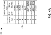
- a first layer (identified as coating run 1) is associated with a layer thickness for hydrogenated silicon of approximately 92.633 nm, which exceeds the threshold layer thickness, and is thus deposited using hydrogenated silicon.
- a fourth layer is associated with a layer thickness for hydrogenated silicon of approximately 9.617 nm, which exceeds the threshold layer thickness, and is thus deposited using hydrogenated silicon.
- a fifth layer is associated with a layer thickness for hydrogenated silicon of approximately 4.809 nm, which does not exceed the threshold layer thickness.
- niobium titanium oxide NbTiOx
- a layer thickness of approximately 11.800 nm e.g., based on a refractive index of niobium titanium oxide
- another oxide material may be utilized, such as silicon dioxide (SiO2), niobium pentoxide (Nb 2 O 5 ), tantalum pentoxide (Ta 2 O 5 ), titanium dioxide (TiO 2 ), aluminum oxide (Al 2 O 3 ), zirconium oxide (ZrO 2 ), yttrium oxide (Y 2 O 3 ), hafnium dioxide (HfO 2 ), or the like;
- a nitride material may be used, such as silicon nitride (Si3N4);
- a fluoride material may be used, such as magnesium fluoride (MgF);
- a sulfide material may be used, such as zinc sulfide (ZnS); a selenide material may be used, such as zinc selenide (ZnSe); a combination thereof; or the like.
- a different layer thickness is selected to deposit the fifth layer using niobium titanium oxide. For example, a layer thickness of approximately 11.800 nm is selected for the fifth layer of the spacer based on the refractive index of niobium titanium oxide and a center wavelength for channels associated with the fifth layer. Similarly, a sixth layer and a seventh layer are associated with a layer thickness for hydrogenated silicon of approximately 2.404 nm and approximately 1.202 nm, respectively, which do not exceed the threshold layer thickness.
- the sixth layer and the seventh layer are deposited using niobium titanium oxide with a layer thickness of approximately 5.900 nm and approximately 2.950 nm, respectively, based on the refractive index of niobium titanium oxide and a center wavelength for channels associated with the sixth layer and the seventh layer.
- filter 410 may be associated with a threshold quantity of channels formed by layers of the spacer, such as greater than or equal to 8 channels, 16 channels, 32 channels, 64 channels, 128 channels, 256 channels, or the like.
- a thickness of a second material for a spacer (e.g., the first material being, for example, hydrogenated silicon)
- the thickness is different from an expected thickness based on dispersion values.
- a mixed spacer based filter e.g., filter 410 using a controlled composition is improved relative to another filter (e.g., filter 210) using an uncontrolled composition, based on increasing a thickness of the thinnest layers of the filter and based on enabling manufacture of a filter array using an additive process.
- a filter response is provided for a 64 channel filter array using filter 410.
- filter 410 based on utilizing a mixed spacer layer with oxide layers and hydrogenated silicon layers, filter 410 provides a set of 64 approximately evenly spaced channels covering the wavelength range of approximately 800 nm to approximately 1100 nm, with the set of channels being associated with a transmittance of between approximately 80% and approximately 100%.
- Use of oxide layers rather than hydrogenated silicon layers of less than a threshold layer thickness avoids oxidation, which avoids the grouping of channels shown in Fig. 3B .
- utilization of a mixed spacer improves filter performance of a multispectral filter, and improves optical performance of an optical device that includes filter 410 relative to an all hydrogenated silicon spacer based design.
- filter 410 results in a relatively even spacing of center wavelengths of channels of filter 410 (e.g., a center wavelength spacing that is associated with a deviation of less than a threshold separation for each channel, such as less than approximately 10 nm, less than approximately 6 nm, less than approximately 5 nm, or the like).
- center wavelengths for filter 410 correspond to the theoretical case for filter 210 from a center wavelength of 800 nm at channel index number 0 to a center wavelength of 1100 nm for channel index number 63.
- filter 210 is associated with a channel spacing of between approximately 4.5 nm and approximately 5 nm.
- filter 210 is associated with a channel spacing of between approximately 0.5 nm (e.g., for adjacent channels of a channel group) and approximately 35 nm (e.g., for adjacent channels of different channel groups).
- filter 410 in the actual case is associated with a channel spacing of between approximately 4 nm and approximately 6 nm. In this way, an improvement in a uniformity of channel spacing is achieved by filter 410 relative to filter 210.
- FIGS. 4A-4E are provided merely as examples. Other examples are possible and may differ from what was described with regard to Figs. 4A-4E .
- Figs. 5A and 5B are diagrams relating to a filter with a mixed spacer using an oxide based material for one or more optical filter layers of the mixed spacer.
- a refractive index is provided for a set of spacer materials at a set of wavelengths of light.
- a refractive index of hydrogenated silicon at approximately 800 nm is approximately 3.852, at approximately 930 nm is approximately 3.7225, and at 1100 nm is approximately 3.639.
- respective refractive indices at approximately 800 are approximately 2.342 and approximately 1.469, at approximately 930 nm are approximately 2.323 and approximately 1.466, and at 1100 nm are approximately 2.308 and approximately 1.464.
- a change in refractive index for a change in wavelength is different for niobium titanium oxide and silicon dioxide relative to hydrogenated silicon.
- hydrogenated silicon is associated with a reduction of approximately 3.4% and approximately 5.5% in refractive index at a change in wavelength from approximately 800 nm to approximately 930 nm and approximately 1100 nm, respectively.
- niobium titanium oxide is associated with a reduction of approximately 0.8% and approximately 1.5%
- silicon dioxide is associated with a reduction or approximately 0.2% and approximately 0.3%.
- a result of the mismatch between the change in refractive index of hydrogenated silicon and the change in refractive index of niobium titanium oxide or silicon dioxide is a change to a uniformity in channel spacing.
- channel spacing for filter 410 exhibits a deviation of linearity relative to the theoretical channel spacing for filter 210. This deviation of linearity is less than a threshold deviation.
- filter 410 is associated with a channel separation of less than a threshold channel separation (e.g., less than approximately 6 nm).
- FIGS. 5A and 5B are provided merely as examples. Other examples are possible and may differ from what was described with regard to Figs. 5A and 5B .
- Figs. 6A-6D are diagrams relating to a filter with a mixed spacer using an oxide based material for one or more optical filter layers of the mixed spacer.
- a filter 610 may include a first mirror, a set of layers of a spacer, and a second mirror.
- the first mirror and the second mirror may be quarterwave stack mirrors, metal mirrors, or the like. Layers of the spacer are deposited using a set of coating runs (identified as coating runs 1, 2, 3, ).
- Hydrogenated silicon e.g., which may be associated with a refractive index greater than a threshold refractive index at a spectral range of between approximately 800 nm and approximately 1100 nm, such as greater than 2.0, greater than 2.5, greater than 3.0, greater than 3.5, greater than 3.6, or the like
- another material e.g., another oxidizable material
- An oxide e.g., silicon dioxide (SiO 2 )
- SiO 2 silicon dioxide
- a first layer (identified as coating run 1) is associated with a layer thickness for hydrogenated silicon of approximately 92.633 nm, which exceeds the threshold layer thickness, and is thus deposited using hydrogenated silicon.
- a fourth layer is associated with a layer thickness for hydrogenated silicon of approximately 9.617 nm, which exceeds the threshold layer thickness, and is thus deposited using hydrogenated silicon.
- a fifth layer is associated with a layer thickness for hydrogenated silicon of approximately 4.809 nm, which does not exceed the threshold layer thickness.
- silicon dioxide (SiO 2 ) is deposited with a layer thickness of approximately 30.400 nm (e.g., based on a refractive index of silicon dioxide oxide) rather than hydrogenated silicon.
- a different layer thickness is selected to deposit the fifth layer using silicon dioxide. For example, a layer thickness of approximately 30.4 nm is selected for the fifth layer of the spacer based on the refractive index of silicon dioxide and a center wavelength for channels associated with the fifth layer. Similarly, a sixth layer and a seventh layer are associated with a layer thickness for hydrogenated silicon of approximately 2.404 nm and approximately 1.202 nm, respectively, which do not exceed the threshold layer thickness.
- the sixth layer and the seventh layer are deposited using silicon dioxide with a layer thickness of approximately 15.2 nm and approximately 7.6 nm, respectively, based on the refractive index of silicon dioxide and a center wavelength for channels associated with the sixth layer and the seventh layer.
- filter 610 may be associated with a threshold quantity of channels formed by layers of the spacer, such as greater than or equal to 8 channels, 16 channels, 32 channels, 64 channels, 128 channels, 256 channels, or the like.
- a filter response is provided for a 63 channel filter array using filter 610.
- filter 610 based on utilizing a mixed spacer layer with oxide layers and hydrogenated silicon layers, filter 610 provides a set of 63 approximately evenly spaced channels covering the wavelength range of approximately 800 nm to approximately 1100 nm, with the set of channels being associated with a transmittance of between approximately 60% and approximately 95%.
- Use of oxide layers rather than hydrogenated silicon layers of less than a threshold layer thickness avoids oxidation, which avoids the grouping of channels shown in, for example, Fig. 3B .
- utilization of a mixed spacer improves filter performance of a multispectral filter, and improves optical performance of an optical device that includes filter 610 relative to an all hydrogenated silicon spacer based design.
- filter 610 results in a relatively even spacing of center wavelengths of channels of filter 610 (e.g., a center wavelength spacing that is associated with a deviation of less than a threshold separation for each channel, such as less than approximately 10 nm, less than approximately 6 nm, less than approximately 5 nm, or the like).
- center wavelengths for filter 610 correspond to the theoretical case for filter 210 from a center wavelength of 800 nm at channel index number 0 to a center wavelength of 1100 nm for channel index number 63.
- filter 610 is associated with 63 channels based on a particular set of channels (e.g., channel numbers 7 and 8) being associated with a common center wavelength based on a dispersion mismatch between hydrogenated silicon and silicon dioxide.
- chart 640 in contrast to chart 330 in Fig.
- filter 210 is associated with a channel spacing of between approximately 0.5 nm (e.g., for adjacent channels of a channel group) and approximately 35 nm (e.g., for adjacent channels of different channel groups), for filter 610 in the actual case, a channel spacing of between approximately 0 nm and approximately 7 nm, between approximately 4 nm and approximately 7 nm, between approximately 4.5 nm and approximately 5.0 nm, or the like is achieved. In this way, an improvement in a uniformity of channel spacing is achieved by filter 610 relative to filter 210.
- FIGS. 6A-6D are provided merely as examples. Other examples are possible and may differ from what was described with regard to Figs. 6A-6D .
- satisfying a threshold may refer to a value being greater than the threshold, more than the threshold, higher than the threshold, greater than or equal to the threshold, less than the threshold, fewer than the threshold, lower than the threshold, less than or equal to the threshold, equal to the threshold, etc.
Landscapes
- Physics & Mathematics (AREA)
- General Physics & Mathematics (AREA)
- Optics & Photonics (AREA)
- Optical Filters (AREA)
- Light Receiving Elements (AREA)
- Spectrometry And Color Measurement (AREA)
Applications Claiming Priority (1)
| Application Number | Priority Date | Filing Date | Title |
|---|---|---|---|
| US15/601,740 US11137527B2 (en) | 2017-05-22 | 2017-05-22 | Mixed spacer multispectral filter |
Publications (2)
| Publication Number | Publication Date |
|---|---|
| EP3407102A1 true EP3407102A1 (fr) | 2018-11-28 |
| EP3407102B1 EP3407102B1 (fr) | 2024-03-06 |
Family
ID=62116738
Family Applications (1)
| Application Number | Title | Priority Date | Filing Date |
|---|---|---|---|
| EP18170858.7A Active EP3407102B1 (fr) | 2017-05-22 | 2018-05-04 | Filtre multispectral d'espacement mixte |
Country Status (8)
| Country | Link |
|---|---|
| US (1) | US11137527B2 (fr) |
| EP (1) | EP3407102B1 (fr) |
| JP (1) | JP7282484B2 (fr) |
| KR (1) | KR102571386B1 (fr) |
| CN (1) | CN108931831B (fr) |
| CA (1) | CA3002986A1 (fr) |
| HK (2) | HK1256270A1 (fr) |
| TW (1) | TWI766013B (fr) |
Families Citing this family (1)
| Publication number | Priority date | Publication date | Assignee | Title |
|---|---|---|---|---|
| US11209311B2 (en) * | 2020-03-18 | 2021-12-28 | Viavi Solutions Inc. | Multispectral filter |
Citations (7)
| Publication number | Priority date | Publication date | Assignee | Title |
|---|---|---|---|---|
| JPS62267624A (ja) * | 1986-05-15 | 1987-11-20 | Minolta Camera Co Ltd | 分光測定センサ |
| US20040080830A1 (en) * | 2002-10-25 | 2004-04-29 | Charles Leu | Niobium oxide and silicon dioxide thin film filter for dense wavelength division multiplexing |
| US20080042782A1 (en) * | 2005-04-27 | 2008-02-21 | Shanghai Institute Of Technical Physics, Chinese Academy Of Sciences | Integrated narrow bandpass filter array and a method for fabrication thereof |
| US20140014838A1 (en) * | 2012-07-16 | 2014-01-16 | Karen Denise Hendrix | Optical filter and sensor system |
| US20160238759A1 (en) * | 2015-02-18 | 2016-08-18 | Materion Corporation | Near infrared optical interference filters with improved transmission |
| US20170108631A1 (en) * | 2014-06-30 | 2017-04-20 | Asahi Glass Company, Limited | Band-pass filter |
| EP3187909A1 (fr) * | 2015-12-29 | 2017-07-05 | Viavi Solutions Inc. | Réseau de filtres multispectraux à base de miroir métallique |
Family Cites Families (24)
| Publication number | Priority date | Publication date | Assignee | Title |
|---|---|---|---|---|
| JPH0786569B2 (ja) * | 1987-08-26 | 1995-09-20 | 東芝ライテック株式会社 | 管 球 |
| US5398133A (en) * | 1993-10-27 | 1995-03-14 | Industrial Technology Research Institute | High endurance near-infrared optical window |
| JP4111288B2 (ja) * | 1998-07-09 | 2008-07-02 | Tdk株式会社 | 波長選択型光検出器 |
| GB9901858D0 (en) * | 1999-01-29 | 1999-03-17 | Secr Defence | Optical filters |
| US7138156B1 (en) * | 2000-09-26 | 2006-11-21 | Myrick Michael L | Filter design algorithm for multi-variate optical computing |
| US20050231800A1 (en) * | 2001-12-21 | 2005-10-20 | Barret Lippey | Selective reflecting |
| JP2004138798A (ja) * | 2002-10-17 | 2004-05-13 | Sun Tec Kk | 誘電体多層膜バンドパスフィルタ |
| AU2003288275A1 (en) * | 2002-11-05 | 2004-06-07 | N.V. Bekaert S.A. | Optical filter |
| EP1671177A1 (fr) * | 2003-10-07 | 2006-06-21 | Aegis Semiconductor, Inc. | Filtre optique accordable dote d'un dispositif de chauffage sur un substrat transparent repondant au coefficient de dilatation thermique |
| US7901870B1 (en) * | 2004-05-12 | 2011-03-08 | Cirrex Systems Llc | Adjusting optical properties of optical thin films |
| CN101361011A (zh) * | 2005-11-05 | 2009-02-04 | 3M创新有限公司 | 包括高折射率涂层和抗反射涂层的光学薄膜 |
| WO2008108784A2 (fr) * | 2006-05-23 | 2008-09-12 | Regents Of The Uninersity Of Minnesota | Détecteurs thermiques de cavité infrarouge à finesse ajustable |
| US20080055717A1 (en) * | 2006-09-01 | 2008-03-06 | Atul Pradhan | Optical transmission filter with extended out-of-band blocking |
| JP2008070437A (ja) * | 2006-09-12 | 2008-03-27 | Matsushita Electric Ind Co Ltd | 干渉フィルタ、液晶ディスプレイ、エレクトロルミネッセンスディスプレイ、プロジェクション表示装置 |
| US20080280147A1 (en) * | 2007-05-09 | 2008-11-13 | Thiel James P | Vehicle transparency |
| EP2522968B1 (fr) * | 2009-11-30 | 2021-04-21 | IMEC vzw | Circuit intégré pour système d'imagerie spectrale |
| JP2014515839A (ja) * | 2011-04-20 | 2014-07-03 | ザ・リージェンツ・オブ・ザ・ユニバーシティ・オブ・ミシガン | 最小角度依存性を有する表示装置及びイメージング用のスペクトルフィルタリング |
| US20140272217A1 (en) * | 2013-03-18 | 2014-09-18 | Apple Inc. | Methods and structures for thermal management in an electronic device |
| TWI668216B (zh) * | 2014-10-08 | 2019-08-11 | 日商日本觸媒股份有限公司 | Oxygen-carbon compound, resin composition containing the same, and filter containing the resin composition |
| US9823395B2 (en) * | 2014-10-17 | 2017-11-21 | 3M Innovative Properties Company | Multilayer optical film having overlapping harmonics |
| US9989684B2 (en) * | 2015-01-23 | 2018-06-05 | Materion Corporation | Near infrared optical interference filters with improved transmission |
| US10345499B2 (en) * | 2015-02-03 | 2019-07-09 | Vitro Flat Glass LLC.. | Solar control coating with enhanced solar control performance |
| US10539726B2 (en) * | 2015-09-01 | 2020-01-21 | Vitro Flat Glass Llc | Solar control coating with enhanced solar control performance |
| EP3182079B1 (fr) * | 2015-12-14 | 2023-08-23 | ams AG | Dispositif de détection optique et procédé de fabrication d'un tel appareil |
-
2017
- 2017-05-22 US US15/601,740 patent/US11137527B2/en active Active
-
2018
- 2018-04-27 JP JP2018087601A patent/JP7282484B2/ja active Active
- 2018-04-27 CA CA3002986A patent/CA3002986A1/fr active Pending
- 2018-05-02 TW TW107114882A patent/TWI766013B/zh active
- 2018-05-04 EP EP18170858.7A patent/EP3407102B1/fr active Active
- 2018-05-21 KR KR1020180057692A patent/KR102571386B1/ko active IP Right Grant
- 2018-05-22 CN CN201810494139.4A patent/CN108931831B/zh active Active
- 2018-11-29 HK HK18115330.7A patent/HK1256270A1/zh unknown
-
2019
- 2019-01-25 HK HK19101352.9A patent/HK1258879A1/zh unknown
Patent Citations (7)
| Publication number | Priority date | Publication date | Assignee | Title |
|---|---|---|---|---|
| JPS62267624A (ja) * | 1986-05-15 | 1987-11-20 | Minolta Camera Co Ltd | 分光測定センサ |
| US20040080830A1 (en) * | 2002-10-25 | 2004-04-29 | Charles Leu | Niobium oxide and silicon dioxide thin film filter for dense wavelength division multiplexing |
| US20080042782A1 (en) * | 2005-04-27 | 2008-02-21 | Shanghai Institute Of Technical Physics, Chinese Academy Of Sciences | Integrated narrow bandpass filter array and a method for fabrication thereof |
| US20140014838A1 (en) * | 2012-07-16 | 2014-01-16 | Karen Denise Hendrix | Optical filter and sensor system |
| US20170108631A1 (en) * | 2014-06-30 | 2017-04-20 | Asahi Glass Company, Limited | Band-pass filter |
| US20160238759A1 (en) * | 2015-02-18 | 2016-08-18 | Materion Corporation | Near infrared optical interference filters with improved transmission |
| EP3187909A1 (fr) * | 2015-12-29 | 2017-07-05 | Viavi Solutions Inc. | Réseau de filtres multispectraux à base de miroir métallique |
Also Published As
| Publication number | Publication date |
|---|---|
| CN108931831A (zh) | 2018-12-04 |
| JP7282484B2 (ja) | 2023-05-29 |
| HK1256270A1 (zh) | 2019-09-20 |
| JP2018197854A (ja) | 2018-12-13 |
| US20180335556A1 (en) | 2018-11-22 |
| TW201901196A (zh) | 2019-01-01 |
| HK1258879A1 (zh) | 2019-11-22 |
| TWI766013B (zh) | 2022-06-01 |
| CA3002986A1 (fr) | 2018-11-22 |
| EP3407102B1 (fr) | 2024-03-06 |
| CN108931831B (zh) | 2023-08-18 |
| KR20180127932A (ko) | 2018-11-30 |
| US11137527B2 (en) | 2021-10-05 |
| KR102571386B1 (ko) | 2023-08-25 |
Similar Documents
| Publication | Publication Date | Title |
|---|---|---|
| US11880054B2 (en) | Multispectral filter | |
| US11450698B2 (en) | Dielectric mirror based multispectral filter array | |
| TWI713666B (zh) | 基於金屬鏡的多光譜濾光片陣列 | |
| JP2018200464A5 (fr) | ||
| KR20210103444A (ko) | 유도형 투과 필터 | |
| US11143803B2 (en) | Multispectral filter | |
| EP3407102B1 (fr) | Filtre multispectral d'espacement mixte | |
| JP7145086B2 (ja) | 光学フィルタ用の入射角制限 | |
| TWI352219B (en) | An optical filter and a method of making the same |
Legal Events
| Date | Code | Title | Description |
|---|---|---|---|
| PUAI | Public reference made under article 153(3) epc to a published international application that has entered the european phase |
Free format text: ORIGINAL CODE: 0009012 |
|
| STAA | Information on the status of an ep patent application or granted ep patent |
Free format text: STATUS: THE APPLICATION HAS BEEN PUBLISHED |
|
| AK | Designated contracting states |
Kind code of ref document: A1 Designated state(s): AL AT BE BG CH CY CZ DE DK EE ES FI FR GB GR HR HU IE IS IT LI LT LU LV MC MK MT NL NO PL PT RO RS SE SI SK SM TR |
|
| AX | Request for extension of the european patent |
Extension state: BA ME |
|
| STAA | Information on the status of an ep patent application or granted ep patent |
Free format text: STATUS: REQUEST FOR EXAMINATION WAS MADE |
|
| 17P | Request for examination filed |
Effective date: 20190429 |
|
| RBV | Designated contracting states (corrected) |
Designated state(s): AL AT BE BG CH CY CZ DE DK EE ES FI FR GB GR HR HU IE IS IT LI LT LU LV MC MK MT NL NO PL PT RO RS SE SI SK SM TR |
|
| REG | Reference to a national code |
Ref country code: HK Ref legal event code: DE Ref document number: 1256270 Country of ref document: HK |
|
| STAA | Information on the status of an ep patent application or granted ep patent |
Free format text: STATUS: EXAMINATION IS IN PROGRESS |
|
| 17Q | First examination report despatched |
Effective date: 20200108 |
|
| STAA | Information on the status of an ep patent application or granted ep patent |
Free format text: STATUS: EXAMINATION IS IN PROGRESS |
|
| STAA | Information on the status of an ep patent application or granted ep patent |
Free format text: STATUS: EXAMINATION IS IN PROGRESS |
|
| RAP3 | Party data changed (applicant data changed or rights of an application transferred) |
Owner name: VIAVI SOLUTIONS INC. |
|
| P01 | Opt-out of the competence of the unified patent court (upc) registered |
Effective date: 20230530 |
|
| GRAP | Despatch of communication of intention to grant a patent |
Free format text: ORIGINAL CODE: EPIDOSNIGR1 |
|
| STAA | Information on the status of an ep patent application or granted ep patent |
Free format text: STATUS: GRANT OF PATENT IS INTENDED |
|
| INTG | Intention to grant announced |
Effective date: 20230811 |
|
| RIN1 | Information on inventor provided before grant (corrected) |
Inventor name: OCKENFUSS, GEORG J. Inventor name: SWITZER III, JAMES |
|
| GRAS | Grant fee paid |
Free format text: ORIGINAL CODE: EPIDOSNIGR3 |
|
| GRAJ | Information related to disapproval of communication of intention to grant by the applicant or resumption of examination proceedings by the epo deleted |
Free format text: ORIGINAL CODE: EPIDOSDIGR1 |
|
| GRAL | Information related to payment of fee for publishing/printing deleted |
Free format text: ORIGINAL CODE: EPIDOSDIGR3 |
|
| STAA | Information on the status of an ep patent application or granted ep patent |
Free format text: STATUS: EXAMINATION IS IN PROGRESS |
|
| GRAP | Despatch of communication of intention to grant a patent |
Free format text: ORIGINAL CODE: EPIDOSNIGR1 |
|
| STAA | Information on the status of an ep patent application or granted ep patent |
Free format text: STATUS: GRANT OF PATENT IS INTENDED |
|
| INTC | Intention to grant announced (deleted) | ||
| INTG | Intention to grant announced |
Effective date: 20240104 |
|
| GRAA | (expected) grant |
Free format text: ORIGINAL CODE: 0009210 |
|
| STAA | Information on the status of an ep patent application or granted ep patent |
Free format text: STATUS: THE PATENT HAS BEEN GRANTED |
|
| AK | Designated contracting states |
Kind code of ref document: B1 Designated state(s): AL AT BE BG CH CY CZ DE DK EE ES FI FR GB GR HR HU IE IS IT LI LT LU LV MC MK MT NL NO PL PT RO RS SE SI SK SM TR |
|
| REG | Reference to a national code |
Ref country code: GB Ref legal event code: FG4D |
|
| REG | Reference to a national code |
Ref country code: CH Ref legal event code: EP |
|
| REG | Reference to a national code |
Ref country code: DE Ref legal event code: R096 Ref document number: 602018066113 Country of ref document: DE |
|
| REG | Reference to a national code |
Ref country code: IE Ref legal event code: FG4D |