EP3399504B1 - Magnetic image sensor - Google Patents
Magnetic image sensor Download PDFInfo
- Publication number
- EP3399504B1 EP3399504B1 EP16881103.2A EP16881103A EP3399504B1 EP 3399504 B1 EP3399504 B1 EP 3399504B1 EP 16881103 A EP16881103 A EP 16881103A EP 3399504 B1 EP3399504 B1 EP 3399504B1
- Authority
- EP
- European Patent Office
- Prior art keywords
- resistance
- magnetic
- configuration
- image sensor
- substrate
- Prior art date
- Legal status (The legal status is an assumption and is not a legal conclusion. Google has not performed a legal analysis and makes no representation as to the accuracy of the status listed.)
- Active
Links
Images




Classifications
-
- G—PHYSICS
- G01—MEASURING; TESTING
- G01R—MEASURING ELECTRIC VARIABLES; MEASURING MAGNETIC VARIABLES
- G01R33/00—Arrangements or instruments for measuring magnetic variables
- G01R33/02—Measuring direction or magnitude of magnetic fields or magnetic flux
- G01R33/06—Measuring direction or magnitude of magnetic fields or magnetic flux using galvano-magnetic devices
- G01R33/09—Magnetoresistive devices
- G01R33/091—Constructional adaptation of the sensor to specific applications
-
- G—PHYSICS
- G01—MEASURING; TESTING
- G01R—MEASURING ELECTRIC VARIABLES; MEASURING MAGNETIC VARIABLES
- G01R33/00—Arrangements or instruments for measuring magnetic variables
- G01R33/0094—Sensor arrays
-
- G—PHYSICS
- G01—MEASURING; TESTING
- G01R—MEASURING ELECTRIC VARIABLES; MEASURING MAGNETIC VARIABLES
- G01R33/00—Arrangements or instruments for measuring magnetic variables
- G01R33/02—Measuring direction or magnitude of magnetic fields or magnetic flux
- G01R33/06—Measuring direction or magnitude of magnetic fields or magnetic flux using galvano-magnetic devices
- G01R33/09—Magnetoresistive devices
-
- G—PHYSICS
- G01—MEASURING; TESTING
- G01R—MEASURING ELECTRIC VARIABLES; MEASURING MAGNETIC VARIABLES
- G01R33/00—Arrangements or instruments for measuring magnetic variables
- G01R33/02—Measuring direction or magnitude of magnetic fields or magnetic flux
- G01R33/06—Measuring direction or magnitude of magnetic fields or magnetic flux using galvano-magnetic devices
- G01R33/09—Magnetoresistive devices
- G01R33/093—Magnetoresistive devices using multilayer structures, e.g. giant magnetoresistance sensors
-
- G—PHYSICS
- G01—MEASURING; TESTING
- G01R—MEASURING ELECTRIC VARIABLES; MEASURING MAGNETIC VARIABLES
- G01R33/00—Arrangements or instruments for measuring magnetic variables
- G01R33/02—Measuring direction or magnitude of magnetic fields or magnetic flux
- G01R33/06—Measuring direction or magnitude of magnetic fields or magnetic flux using galvano-magnetic devices
- G01R33/09—Magnetoresistive devices
- G01R33/096—Magnetoresistive devices anisotropic magnetoresistance sensors
-
- G—PHYSICS
- G01—MEASURING; TESTING
- G01R—MEASURING ELECTRIC VARIABLES; MEASURING MAGNETIC VARIABLES
- G01R33/00—Arrangements or instruments for measuring magnetic variables
- G01R33/02—Measuring direction or magnitude of magnetic fields or magnetic flux
- G01R33/06—Measuring direction or magnitude of magnetic fields or magnetic flux using galvano-magnetic devices
- G01R33/09—Magnetoresistive devices
- G01R33/098—Magnetoresistive devices comprising tunnel junctions, e.g. tunnel magnetoresistance sensors
-
- G—PHYSICS
- G07—CHECKING-DEVICES
- G07D—HANDLING OF COINS OR VALUABLE PAPERS, e.g. TESTING, SORTING BY DENOMINATIONS, COUNTING, DISPENSING, CHANGING OR DEPOSITING
- G07D7/00—Testing specially adapted to determine the identity or genuineness of valuable papers or for segregating those which are unacceptable, e.g. banknotes that are alien to a currency
- G07D7/04—Testing magnetic properties of the materials thereof, e.g. by detection of magnetic imprint
-
- G—PHYSICS
- G07—CHECKING-DEVICES
- G07D—HANDLING OF COINS OR VALUABLE PAPERS, e.g. TESTING, SORTING BY DENOMINATIONS, COUNTING, DISPENSING, CHANGING OR DEPOSITING
- G07D7/00—Testing specially adapted to determine the identity or genuineness of valuable papers or for segregating those which are unacceptable, e.g. banknotes that are alien to a currency
- G07D7/20—Testing patterns thereon
-
- G—PHYSICS
- G01—MEASURING; TESTING
- G01R—MEASURING ELECTRIC VARIABLES; MEASURING MAGNETIC VARIABLES
- G01R33/00—Arrangements or instruments for measuring magnetic variables
- G01R33/0023—Electronic aspects, e.g. circuits for stimulation, evaluation, control; Treating the measured signals; calibration
- G01R33/0029—Treating the measured signals, e.g. removing offset or noise
-
- G—PHYSICS
- G01—MEASURING; TESTING
- G01R—MEASURING ELECTRIC VARIABLES; MEASURING MAGNETIC VARIABLES
- G01R33/00—Arrangements or instruments for measuring magnetic variables
- G01R33/0052—Manufacturing aspects; Manufacturing of single devices, i.e. of semiconductor magnetic sensor chips
-
- G—PHYSICS
- G01—MEASURING; TESTING
- G01R—MEASURING ELECTRIC VARIABLES; MEASURING MAGNETIC VARIABLES
- G01R33/00—Arrangements or instruments for measuring magnetic variables
- G01R33/02—Measuring direction or magnitude of magnetic fields or magnetic flux
- G01R33/06—Measuring direction or magnitude of magnetic fields or magnetic flux using galvano-magnetic devices
- G01R33/07—Hall effect devices
-
- G—PHYSICS
- G01—MEASURING; TESTING
- G01R—MEASURING ELECTRIC VARIABLES; MEASURING MAGNETIC VARIABLES
- G01R33/00—Arrangements or instruments for measuring magnetic variables
- G01R33/12—Measuring magnetic properties of articles or specimens of solids or fluids
-
- G—PHYSICS
- G07—CHECKING-DEVICES
- G07D—HANDLING OF COINS OR VALUABLE PAPERS, e.g. TESTING, SORTING BY DENOMINATIONS, COUNTING, DISPENSING, CHANGING OR DEPOSITING
- G07D2207/00—Paper-money testing devices
Definitions
- the disclosure relates to the field of sensors, and particularly to a magnetic image sensor.
- Producing specific magnetic information on a medium such as paper money, a note and a negotiable security is one of important means of a modern anti-counterfeiting technology.
- a magnetic information anti-counterfeiting technology is continuously enhanced.
- banknotes of many countries such as Renminbi, U.S. dollars, Euros, so on
- Recognition over the specific magnetic information on the medium such as the paper money, the note and the negotiable security is also necessary anti-counterfeiting detection means.
- a magnetic image sensor In order to implement detection, a magnetic image sensor is provided in a related technology.
- miniature magnetic heads are continuously arranged in the whole reading and recognition range to form a linear array of the miniature magnetic heads, thereby implementing reading and recognition on magnetic information in the whole reading range.
- each single magnetic head is relatively larger in size, and a reading and recognition range on each magnetic head occupies a small part of a range of the magnetic head, so that a large range between the magnetic heads are outside a effective reading range of the magnetic heads, that is, it is impossible to read the region between the magnetic heads.
- the magnetic information at a gap between the magnetic heads may get lost.
- a magnetic sensing device is further provided in the related technology.
- Multiple recesses linearly formed along a side length direction of an internal bracket are formed in an upper surface of the internal bracket of the magnetic sensing device.
- a magneto-resistive element is accommodated in each recess, and the magneto-resistive elements are arranged into a linear array within a reading and recognition range to read and recognize magnetic information in the reading range.
- the magnetic head is replaced with the magneto-resistive element, and the gap between the magneto-resistive elements is greatly reduced, so that the whole magnetic sensing device is miniaturized.
- the magneto-resistive element has an excessively large linear dimension, the magnetic information in the range of the dimension is not able to be distinguished in detail, the read magnetic information on a medium is very blurred, and details of the magnetic information is not able to be distinguished. Therefore, when finer characteristics of magnetic information regions are required to be judged, this magnetic sensing device is incapable.
- Magnetic sensing elements are array magnetic sensing elements which used for reading magnetic characteristics of a medium. Magnetic sensing elements are configured at an end part of a plane sidewall of one side of a frame along a direction of a reading range, and the magnetic sensing element is point-like or strip-type.
- a resolution of the magnetic sensing elements manufactured by a printing sintering process is able to reach more than 50DPI, so that a problem about a magnetic information resolution capability is solved.
- a deviation of the magnetic sensing elements obtained by the printing sintering process is very great, usually about 20%, and even though the magnetic resistance deviation is reduced by a method for changing a resistance, the deviation may also be about 3%-5%.
- a voltage deviation of an order of magnitude of at least 150mV is produced.
- a magnetic Signal voltage which is able to be detected practically is usually with an order of magnitude of 10mV, that is, a signal difference (noise signal) caused by a practical magnetic resistance deviation is far greater than an effective signal, so that a great difficulty is brought to signal processing, and it is very difficult to accurately separate the effective signal from the noise signal under a normal condition.
- the invention is mainly intended to provide a magnetic image sensor, so as to solve the problem of relatively stronger noise signal caused by a magnetic resistance deviation of a magnetic image sensor in the related technology.
- the invention provides a magnetic image sensor according to claim 1.
- the configuration resistance is connected with the magnetic resistance (1) in a one-to-one corresponding manner.
- the resistance value of the configuration resistance is adjusted to be consistent with a resistance value of the corresponding magnetic resistance.
- the magnetic image sensor further comprises: a configuration resistance substrate, wherein the configuration resistance is arranged on the configuration resistance substrate; a loading substrate, wherein the magnetic resistance and the driving circuit are arranged on the loading substrate; and a connecting substrate, wherein the configuration resistance substrate and the loading substrate are arranged on the connecting substrate.
- the configuration resistance substrate is a substrate manufactured by a ceramic material, and a protective film is arranged on the configuration resistance.
- a connecting pad is arranged on the loading substrate, and the configuration resistance comprises: a common electrode and an individual electrode, wherein the individual electrode is connected with the magnetic resistance in a one-to-one corresponding manner on the connecting pad through a connecting wire.
- the configuration resistance refers to multiple configuration resistances
- the common electrode refers to multiple common electrodes
- each common electrode in the multiple common electrodes is shared by two configuration resistances in the multiple configuration resistances, or, an independent electrode is arranged between every two adjacent configuration resistances in the multiple configuration resistances, and each configuration resistance is provided with an independent common electrode branch.
- the magnetic resistance is a Tunneling Magnetic Resistance (TMR) manufactured on a semiconductor silicon wafer by vacuum coating, and a first pad and a second pad are configured to connect two ends of the TMR.
- TMR Tunneling Magnetic Resistance
- the driving circuit (3) comprises: a shift register circuit (3a), and a switching circuit (3b), configured to be turned on to receive the changed magnetic signal detected by the magnetic resistance (1), wherein the magnetic image sensor further comprises: a signal amplification circuit (4), configured to receive a serial SIG output by the driving circuit (3) and perform amplification processing on the serial SIG.
- the magnetic image sensor including the following structures: a magnetic resistance, arranged along a scanning direction and configured to detect a changed magnetic signal in a range to be detected; a configuration resistance, connected with the magnetic resistance, wherein a resistance value of the configuration resistance is adjustable; and a driving circuit (3), connected with the magnetic resistance and configured to perform output control on the changed magnetic signal detected by the magnetic resistance.
- the configuration resistance value with adjustable resistance is connected with the magnetic resistance, so that the problem of relatively stronger noise signal caused by a magnetic resistance deviation of a magnetic image sensor in the related technology is solved, and an effect of reducing the noise signal of the magnetic image sensor is further achieved.
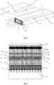
- Fig. 1 is a sectional view of a magnetic image sensor according to the invention.
- Fig. 2 is an internal top view of a magnetic image sensor according to an embodiment of the disclosure.
- the magnetic image sensor includes a magnetic resistance 1, a configuration resistance 2 and a driving circuit 3.
- the magnetic resistance 1 is arranged along a scanning direction, and is configured to detect a changed magnetic signal in a range to be detected.
- the magnetic resistance 1 may be one or more magnetic resistances 1.
- the magnetic resistance 1 may be multiple magnetic resistances 1, and the multiple magnetic resistances 1 are linearly arranged along the scanning direction.
- the magnetic resistance 1 of the embodiment of the disclosure is a Tunnel Magnetic Resistance, TMR manufactured by a semiconductor process.
- the resistance value of the configuration resistance 2 is adjustable, and may be paired with the magnetic resistance 1 for use.
- the configuration resistance 2 may be one or more configuration resistances 2.
- the multiple configuration resistances 2 are linearly arranged, and the multiple configuration resistances 2 are connected with the multiple magnetic resistances 1 in a one-to-one corresponding manner.
- the driving circuit 3 is configured to perform output control on the changed magnetic signal detected by the magnetic resistance 1, including: to transmit a magnetic field signal detected by the magnetic resistance 1 and to control output of the magnetic field signal.
- each configuration resistance 2 in the embodiment of the disclosure may include one or more segments of resistance bodies.
- the driving circuit 3 may also be multiple. Each driving circuit 3 in the multiple driving circuits 3 may control multiple magnetic sensing pixels.
- the multiple driving circuits 3 are sequentially connected and arranged to perform output control on a signal of the magnetic sensing pixels in the whole detection range.
- the magnetic image sensor may further include a signal amplification circuit 4, wherein the signal amplification circuit 4 is configured to perform amplification processing on the detected magnetic signal (for example, a voltage signal converted by the magnetic resistance 1 and the configuration resistance 2).
- the signal amplification circuit 4 is configured to perform amplification processing on the detected magnetic signal (for example, a voltage signal converted by the magnetic resistance 1 and the configuration resistance 2).
- the magnetic image sensor may further include a magnet 5, wherein the magnet 5 is arranged within the magnetic image sensor.
- S and N are two poles of the magnets, and the magnet 5 is configured to generate a longitudinal magnetic field.
- the magnet 5 is arranged along the scanning direction, and is arranged below the magnetic resistance 1.
- a centerline of the magnet 5 corresponds to the magnetic resistance 1.
- the configuration resistance 2 may be arranged on a configuration resistance substrate 20.
- the configuration resistance 2 is manufactured on the configuration resistance substrate 20, and a protective film 23 may also be arranged on the configuration resistance 2.
- the magnetic resistance 1 and the driving circuit 3 may be arranged on a loading substrate 30, and both the configuration resistance substrate 20 and the loading substrate 30 may be arranged on a connecting substrate 10.
- the connecting substrate 10 may be a nonmagnetic substrate, and is configured to carry the loading substrate 30 and the configuration resistance substrate 20.
- the magnetic resistance 1 and the driving circuit 3 are connected with the substrate through a connecting wire 31, wherein the connecting wire 31 may be a gold wire or an aluminum wire frequently used for a semiconductor process and connected by a pressure welding process, and is configured to electrically connect the loading substrate 30 with the configuration resistance substrate 20.
- a protective layer 32 may further be arranged in the magnetic image sensor. After electrical connection with the connecting wire 31 is completed, the protective layer 32 is manufactured to protect the magnetic resistance 1, the driving circuit 3 and the connecting wire 31.
- the magnet 5 and the substrates may be arranged in a frame 6, wherein the frame 6 is configured to accommodate the magnet and various substrates.
- a cover plate 7 is arranged on the frame 6, and the cover plate 7 is configured to protect the magnetic resistance 1, the configuration resistance 2 and the driving circuit 3.
- An object to be detected (such as paper money) passes through an upper surface of the cover plate 7, a magnetic signal on the object to be detected is detected by the magnetic sensing pixel, and a corresponding signal is output.
- the magnetic image sensor provided by the invention, with adoption of the configuration resistance value with an adjustable resistance, noise of the magnetic image sensor can be reduced, and optionally, the accuracy of reading a signal is improved.
- Fig. 2 is a top view of an internal structure of the magnetic image sensor without the cover plate 7. For clarity, only main parts of the magnetic image sensors are shown in the figure.
- the magnetic image sensor includes the frame 6, as well as the configuration resistance substrate 20, configuration resistance 2, loading substrate 30, magnetic resistance 1 and driving circuit 3 which are mounted therein.
- the magnetic resistances 1, configuration resistances 2 and driving circuits 3 are composed of multiple, and they are arranged in a straight line along the scanning direction respectively.
- FIG. 3 is an overall structure diagram of a magnetic image sensor according to an embodiment of the disclosure, wherein the sectional view is shown on one side.
- a detection position 8 is a signal detection position of the magnetic image sensor, and the detection position 8 is a position in the vicinity of an outer surface of the cover plate 7 corresponding to magnetic resistance 1.
- An object to be detected 9 may be a medium such as paper money, a pattern 91 is formed on the object to be detected 9, and the pattern 91 is a pattern with magnetic information on the object to be detected 9.
- the object to be detected 9 moves along the direction of the arrow, and passes through the detection position 8 of the magnetic image sensor, a magnetic signal of the pattern 91 with the magnetic information on the object to be detected 9 changes resistance value of the magnetic resistance 1 in a corresponding region, and resistance value changes of the magnetic resistance 1 is converted into voltage signal through internal circuits.
- the resistance of the magnetic resistance 1 value is not changed, so that a magnetic image on the object to be detected may be detected according to resistance value change conditions of the magnetic resistance 1.
- the magnetic image sensor Under control of the driving circuit 3, the magnetic image sensor detects signal of a line every time, and along with continuous movement of the object to be detected, the magnetic image sensor continuously reads the magnetic image information of the whole picture on the whole object to be detected.
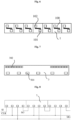
- Fig. 4 is a local enlarged unit diagram of assembled substrates.
- electrodes of the configuration resistance 2 is further arranged on the configuration resistance substrate 20, and include common electrode 21 of the configuration resistance 2 and individual electrode 22 of the configuration resistance 2.
- the individual electrode 22 is connected with the magnetic resistance 1 in the one-to-one corresponding manner on a connecting pad 301 on the loading substrate 30 through the connecting wire 31.
- the common electrode 21 may be connected with the loading substrate 30 at certain positions (not shown in the figure), and voltage signal may also be externally and independently provided for the common electrode 21.
- Fig. 5 is a local enlarged diagram of the configuration resistance substrate 20.
- the configuration resistance substrate 20 is a substrate manufactured from a ceramic material.
- 21a is a branch part, connected with each resistance, of the common electrode 21, and 22a is a part, configured to weld the connecting wire 31, of the individual resistance 22.
- the protective film is protective layers of the configuration resistance 2 and the corresponding electrodes.
- the magnetic image sensor of the embodiment of the disclosure may implement 50DPI magnetic image reading, and an arrangement density of the adopted magnetic resistance 1 and corresponding configuration resistance 2 is 0.5mm.
- the configuration resistance 2 may be continuous resistance bodies formed in a printing manner.
- the configuration resistance 2 of the embodiment of the disclosure is manufactured by adopting a thick film screen printing process.
- a manufacturing process for the configuration resistance is as follows.
- the resistance body is continuous resistance bodies formed in the printing manner, the corresponding electrodes are arranged at lower parts of the resistance body, positions of the electrodes determine positions of the resistance body, and meanwhile, each resistance is formed by two parts from two sides of the individual electrode to the common electrode 21.
- Fig. 6 is another structure of a configuration resistance according to an embodiment of the disclosure. Its basic structure is similar to the embodiment shown in Fig. 5 . However, the independent electrode 24 is designed between the adjacent resistances. In the abovementioned structure, the branch 21a of each common electrode 21 is shared by the corresponding two adjacent resistances. While in the structure, an independent electrode 24 is arranged between every two adjacent configuration resistances 2 in the multiple configuration resistances 2, and each configuration resistance is provided with an independent common electrode branch 21a.Such a structure may reduce influence on the adjacent resistances in a resistance repair process.
- Fig. 7 is a structure diagram of a magnetic resistance according to the invention.
- the magnetic resistance1 adopt TMR 100 manufactured on semiconductor silicon wafers by vacuum coating, and the resistance value of the TMRs 100 is changed in a magnetic field environment along with changes in sizes and directions of magnetic fields.
- Pad 101 and Pad 102 configured to connect two ends of the TMR are arranged at the two ends of the TMR 100, and are configured to electrically connect the TMR with the outside.
- the magnetic resistance adopted in the embodiment of the disclosure may be described with a change relationship curve of resistance value and magnetic fields in the magnetic field environment, axis X may represent the direction and intensity of the magnetic field, and axis Y may represent a magnitude of the resistance value of the resistance.
- Fig. 8 is a structure diagram of a driving circuit 3 according to an embodiment of the disclosure.
- the driving circuit 3 is a long-strip structure.
- Receiving terminals 302 at an upper part transmit the magnetic sensing signal on the magnetic resistance to the inside, and each terminal is connected with a magnetic resistance 1.
- Control terminals at a lower part is configured for circuit control and signal output.
- the driving circuit 3 is structurally 12mm long and 1mm wide, there are 24 receiving terminals at the upper part, which may simultaneously be connected with 25 magnetic resistances 1, and in a scanning process, the signal of the magnetic resistance 1 is sent into the driving circuit 3 through these terminals.
- the control terminals at the lower part besides providing working power, at least include driving signal input terminals SI, driving signal output terminals SO, clock signal CLK, output signal and the like.
- Fig. 9 is a circuit structure diagram of multi-stage connection of driving circuit according to an embodiment of the disclosure.
- a line driving signal SI is input from the SI terminal of the driving circuit 3 at the end part, and is sequentially transmitted backwards in the driving circuit 3 under the action of a clock signal CLK, an internal switch of a receiving terminal therein is turned on every time to transmit the signal on the corresponding magnetic resistance 1 to a signal wire, and the signal is externally output as an output driving signal SO of the driving circuit 3 after passing through a last switch on the driving circuit 3, and is simultaneously input an SI port of the next driving circuit 3 for continuous backward transmission in the driving circuit 3 until being transmitted to all the driving circuit 3.
- the signal on all the magnetic resistance 1 connected with the driving circuit 3 is sequentially transmitted onto the SIG wire to form a line of complete scanning data.
- Fig. 10 is an electrical principle diagram of a magnetic image sensor according to an embodiment of the disclosure.
- the upper ends of the configuration resistance 2 is the common electrode 21 connected with a power supply VDD.
- the individual electrode at the lower ends is connected with the magnetic resistance 1 in the one-to-one corresponding manner.
- the lower ends of the magnetic resistance 1 is the common electrode 2 connected with the Ground (GND).
- a leading-out signal acquisition terminal is arranged between the magnetic resistance 1 and the configuration resistance 2, and is connected with the receiving terminals of the driving circuit 3.
- Each driving circuit 3 includes two parts of functions, 3a is a shift register circuit, and 3b is a switching circuit.
- the driving signal SI is a line driving pulse signal. Switches in the switching circuit 3b are turned on one by one under the action of clocks to input the signal detected by the magnetic resistance 1 into the driving circuit 3, and the driving circuit convert the collected signal into serial signal for external output to a post amplification circuits for signal amplification.
- Fig. 11 is a sequence diagram of a magnetic image sensor according to an embodiment of the disclosure.
- the SI signal is a line driving pulse signal during scanning, every pulse completes scanning of a line
- Vout is an output signal obtained by amplifying the signal by the amplification circuit.
- Internal functions of resetting and the like of the driving circuit 3 require to occupy a certain time, so that the output signal may usually be a few clock periods later than the SI signal, and the resistance value of the magnetic resistance 1 may be increased and may also be decreased according to the intensity and direction of the magnetic field in the scanning environment. Therefore, the output signal may be higher than a reference potential, and may also be lower than the reference potential.
- the magnetic image sensor of the embodiment of the disclosure may be a magnetic image sensor capable of scanning a 192mm width, and internally includes 384 magnetic resistances, and an arrangement period of each magnetic resistance is 0.5mm, so that a 50DPI scanning resolution is formed. Meanwhile, 384 configuration resistances 2 corresponding to the magnetic resistance one to one are arranged, each driving circuit 3 may control 24 magnetic resistances 1, and totally 16 driving circuits are used to drive the 384 magnetic resistances 1.
- VREF0 is a potential of each magnetic resistance without any magnetic field (i.e. a reference potential of each pixel), and the Rm resistance value is changed along with a change of an external magnetic field when there is the external magnetic field, so that a change Vsig in the voltage signal is generated.
- This voltage signal is superposed with the VREF0.
- a signal acquired by the driving circuit 3 between the two resistances is a superposed signal of two voltages, that is, the serial signal output by the driving circuit 3 is VREF0+Vsig.
- a difference of VREF0-VREF is usually required to be larger than a maximum absolute value of Vsig.
- the resistance repair method is adopted for the configuration resistance 2 in the embodiment of the disclosure.
- the configuration resistance 2 is manufactured by sintering the resistance paste including ruthenium oxide as a main component, and a pulse voltage of certain power may be applied to the resistance body to reduce the resistance value (called as resistance value repair for short).
- Fig. 12 is a substrate state and resistance repair principle diagram during resistance repair according to an embodiment of the disclosure.
- the configuration resistance substrate 20 has yet not been connected with the loading substrate 30 through the connecting wire 31, the upper ends of the configuration resistance 2 on the configuration resistance substrate 20 are connected through the common electrode 2, and the individual resistances 22 (22a) at the lower ends are separated. That is, each configuration resistance 2 is independent.
- the magnetic resistance 2 on the loading substrate 30 is connected with the pad 301 and pad 302 on the loading substrate 30 through the connecting wire 31 respectively, but pad 301 and pad 302 are respectively independent, so that the magnetic resistances are also respectively independent at this moment.
- 384 magnetic resistances 1 also called as magnetic sensing pixels sometimes
- a resistance repair method of resistance balancing is adopted to reduce deviations of reference signal between the pixels.
- a specific method is to regulate the Rtn resistance value of all the configuration resistances 2 to be consistent with the Rmn resistance value of the corresponding magnetic resistance 1.
- a design target value of the magnetic resistance 1 is 5K ⁇
- the practical resistance value of the magnetic resistance 1 practically manufactured by a vacuum coating process is between 4K ⁇ -6K ⁇ , if calculated by a maximum deviation of 20%.
- the configuration resistance 2 is printed and sintered from thick film resistance paste, the maximum deviation is about 15%
- the design resistance value of the configuration resistance 2 is set to be 8K ⁇
- the practical resistance value ranges from 6.8K Q -9.2K ⁇ . Because resistance repair of Rt may only reduce the resistance, the practical resistance value of Rt is higher than practical resistance value of Rm.
- Performing resistance repair on thick film resistances is a common method for a thick film resistance manufacturing process.
- target resistance value is usually set, and then resistance of all the resistances is repaired to be the unified resistance value.
- the condition that practical resistance of the thick film resistances value ranges from 6.8K ⁇ -9.2K ⁇ may also be adopted as an example, if the set target resistance value is 5K ⁇ , the resistance value of all the resistances is repaired to be close to 5K ⁇ .
- the resistance repair method adopted in the embodiment of the disclosure is to regulate the Rt resistance value to be consistent with Rm, so that the Rtn target resistance value is the corresponding Rmn resistance value.
- the other is that the resistance value (Rm1 ⁇ Rm384) of all the magnetic resistance 1 is tested and stored in a memory of equipment as target values of the configuration resistance 2 (Rt1 ⁇ Rt384) respectively, and then resistance repair is performed on the configuration resistance 2 one by one.
- a probe contacts with the protective film 23, 22a, pad 301 and pad 302, the resistance Rmn between pad 301 and pad 302 is tested at first, the resistance value is stored in the equipment as a target value of the corresponding configuration resistance 2. Then the resistance between protective film 23 and 22a (initial value before resistance repair) is tested, the initial value is compared with the target value, a certain voltage pulse is applied for resistance repair between protective film 23 and 22a according to a difference value between to reduce the resistance value of the configuration resistance 2.
- resistance repair is performed on the resistance again according to a new difference value, the operations are repeated for many times until the resistance value between protective film 23 and 22a is consistent with the target value, and then resistance repair is performed on the next resistance.
- a magnitude of the signal reference potential may also be regulated by repairing the resistance Rt according to a requirement.
- 22a of the configuration resistance substrate 20 and 301 of the loading substrate 30 are connected through the connecting wire, thereby implementing electrical connection between the two substrates.
- the protective layer 32 is adopted for encapsulation protection over the connecting wire and a bare chip.
- the image sensor of the embodiment adopts a resistance balancing signal detection method, so that the image resolution of the magnetic signal may be ensured, noise of the product may also be greatly reduced, and the signal reading accuracy is improved.
Landscapes
- Physics & Mathematics (AREA)
- General Physics & Mathematics (AREA)
- Condensed Matter Physics & Semiconductors (AREA)
- Measuring Magnetic Variables (AREA)
- Inspection Of Paper Currency And Valuable Securities (AREA)
- Hall/Mr Elements (AREA)
- Transforming Light Signals Into Electric Signals (AREA)
Description
- The disclosure relates to the field of sensors, and particularly to a magnetic image sensor.
- Producing specific magnetic information on a medium such as paper money, a note and a negotiable security is one of important means of a modern anti-counterfeiting technology. Along with development of a production technology, application of a magnetic information anti-counterfeiting technology is continuously enhanced. For example, banknotes of many countries (such as Renminbi, U.S. dollars, Euros, so on) internally include magnetic information with rich content. Recognition over the specific magnetic information on the medium such as the paper money, the note and the negotiable security is also necessary anti-counterfeiting detection means.
- In order to implement detection, a magnetic image sensor is provided in a related technology. In the magnetic image sensor, miniature magnetic heads are continuously arranged in the whole reading and recognition range to form a linear array of the miniature magnetic heads, thereby implementing reading and recognition on magnetic information in the whole reading range. However, each single magnetic head is relatively larger in size, and a reading and recognition range on each magnetic head occupies a small part of a range of the magnetic head, so that a large range between the magnetic heads are outside a effective reading range of the magnetic heads, that is, it is impossible to read the region between the magnetic heads. When such a magnetic image sensor is used, the magnetic information at a gap between the magnetic heads may get lost.
- A magnetic sensing device is further provided in the related technology. Multiple recesses linearly formed along a side length direction of an internal bracket are formed in an upper surface of the internal bracket of the magnetic sensing device. A magneto-resistive element is accommodated in each recess, and the magneto-resistive elements are arranged into a linear array within a reading and recognition range to read and recognize magnetic information in the reading range. In this technology, the magnetic head is replaced with the magneto-resistive element, and the gap between the magneto-resistive elements is greatly reduced, so that the whole magnetic sensing device is miniaturized. However, the magneto-resistive element has an excessively large linear dimension, the magnetic information in the range of the dimension is not able to be distinguished in detail, the read magnetic information on a medium is very blurred, and details of the magnetic information is not able to be distinguished. Therefore, when finer characteristics of magnetic information regions are required to be judged, this magnetic sensing device is incapable.
- A magnetic sensor device is further provided in the related technology. Magnetic sensing elements are array magnetic sensing elements which used for reading magnetic characteristics of a medium. Magnetic sensing elements are configured at an end part of a plane sidewall of one side of a frame along a direction of a reading range, and the magnetic sensing element is point-like or strip-type. In this technology, a resolution of the magnetic sensing elements manufactured by a printing sintering process is able to reach more than 50DPI, so that a problem about a magnetic information resolution capability is solved. However, a deviation of the magnetic sensing elements obtained by the printing sintering process is very great, usually about 20%, and even though the magnetic resistance deviation is reduced by a method for changing a resistance, the deviation may also be about 3%-5%. For a 5V common electrode voltage, a voltage deviation of an order of magnitude of at least 150mV is produced. A magnetic Signal voltage which is able to be detected practically is usually with an order of magnitude of 10mV, that is, a signal difference (noise signal) caused by a practical magnetic resistance deviation is far greater than an effective signal, so that a great difficulty is brought to signal processing, and it is very difficult to accurately separate the effective signal from the noise signal under a normal condition.
- In document
JP 20120 047685 A claim 1, is described, which reads or carries out authenticity determination of the information, such as a magnetic card and a banknote. - For the problem of relatively stronger noise signal caused by a magnetic resistance deviation of a magnetic image sensor in the related technology, No effective solution has been proposed yet.
- The invention is mainly intended to provide a magnetic image sensor, so as to solve the problem of relatively stronger noise signal caused by a magnetic resistance deviation of a magnetic image sensor in the related technology.
- In order to achieve the purpose, the invention provides a magnetic image sensor according to
claim 1. - According to the invention the configuration resistance is connected with the magnetic resistance (1) in a one-to-one corresponding manner.
- According to an example embodiment, the resistance value of the configuration resistance is adjusted to be consistent with a resistance value of the corresponding magnetic resistance.
- According to an example embodiment, the magnetic image sensor as claimed in
claim 1, wherein the configuration resistance is manufactured by adopting a thick film printing process. - According to an example embodiment, the magnetic image sensor further comprises: a configuration resistance substrate, wherein the configuration resistance is arranged on the configuration resistance substrate; a loading substrate, wherein the magnetic resistance and the driving circuit are arranged on the loading substrate; and a connecting substrate, wherein the configuration resistance substrate and the loading substrate are arranged on the connecting substrate.
- According to an example embodiment, the configuration resistance substrate is a substrate manufactured by a ceramic material, and a protective film is arranged on the configuration resistance.
- According to an example embodiment, a connecting pad is arranged on the loading substrate, and the configuration resistance comprises: a common electrode and an individual electrode, wherein the individual electrode is connected with the magnetic resistance in a one-to-one corresponding manner on the connecting pad through a connecting wire.
- According to an example embodiment, the configuration resistance refers to multiple configuration resistances, the common electrode refers to multiple common electrodes, each common electrode in the multiple common electrodes is shared by two configuration resistances in the multiple configuration resistances, or, an independent electrode is arranged between every two adjacent configuration resistances in the multiple configuration resistances, and each configuration resistance is provided with an independent common electrode branch.
- According to the invention, the magnetic resistance is a Tunneling Magnetic Resistance (TMR) manufactured on a semiconductor silicon wafer by vacuum coating, and a first pad and a second pad are configured to connect two ends of the TMR.
- According to an example embodiment, the driving circuit (3) comprises: a shift register circuit (3a), and a switching circuit (3b), configured to be turned on to receive the changed magnetic signal detected by the magnetic resistance (1), wherein the magnetic image sensor further comprises: a signal amplification circuit (4), configured to receive a serial SIG output by the driving circuit (3) and perform amplification processing on the serial SIG.
- According to the disclosure, the magnetic image sensor including the following structures is adopted: a magnetic resistance, arranged along a scanning direction and configured to detect a changed magnetic signal in a range to be detected; a configuration resistance, connected with the magnetic resistance, wherein a resistance value of the configuration resistance is adjustable; and a driving circuit (3), connected with the magnetic resistance and configured to perform output control on the changed magnetic signal detected by the magnetic resistance. The configuration resistance value with adjustable resistance is connected with the magnetic resistance, so that the problem of relatively stronger noise signal caused by a magnetic resistance deviation of a magnetic image sensor in the related technology is solved, and an effect of reducing the noise signal of the magnetic image sensor is further achieved.
- The drawings are adopted to provide a further understanding to the invention as well as other optional disclosure. In the drawings:
-
Fig. 1 shows a sectional view of a magnetic image sensor according to an embodiment of the disclosure; -
Fig. 2 shows an internal top view of a magnetic image sensor according to an embodiment of the disclosure; -
Fig. 3 shows an overall structure diagram of a magnetic image sensor according to an embodiment of the disclosure; -
Fig. 4 shows a local enlarged unit structure diagram of a magnetic image sensor according to an embodiment of the disclosure; -
Fig. 5 shows a local enlarged structure diagram of a ceramic substrate of a magnetic image sensor according to an embodiment of the disclosure; -
Fig. 6 shows another local enlarged structure diagram of a ceramic substrate of a magnetic image sensor according to an embodiment of the disclosure; -
Fig. 7 shows a structure diagram of magnetic signal sensing pixels of a magnetic image sensor according to the invention; -
Fig. 8 shows a structure diagram of a driving circuit of a magnetic image sensor according to an embodiment of the disclosure; -
Fig. 9 shows a circuit structure diagram of multi-stage connection of driving circuit of a magnetic image sensor according to an embodiment of the disclosure; -
Fig. 10 shows a circuit structure diagram of a magnetic image sensor according to an embodiment of the disclosure; -
Fig. 11 shows a sequence diagram of a magnetic image sensor according to an embodiment of the disclosure; and -
Fig. 12 shows a substrate state and resistance repair principle diagram during resistance repair according to an embodiment of the disclosure. - It is important to note that the embodiments in the disclosure and characteristics in the embodiments may be combined without conflicts. The disclosure will be described below with reference to the drawings and in combination with the embodiments in detail.
- In order to make the solution of the disclosure better understood by those skilled in the art, the technical solution in the embodiments of the disclosure will be clearly and completely described below in combination with the drawings in the embodiments of the disclosure.
- It is important to note that terms "first", "second" and the like in the specification, claims and drawings of the disclosure are adopted not to describe a specific sequence or order but to distinguish similar objects. It should be understood that data used like this may be exchanged under a proper condition for implementation of the embodiments of the disclosure described here.
-
Fig. 1 is a sectional view of a magnetic image sensor according to the invention.Fig. 2 is an internal top view of a magnetic image sensor according to an embodiment of the disclosure. - As shown in
Fig. 1 , the magnetic image sensor includes amagnetic resistance 1, aconfiguration resistance 2 and adriving circuit 3. Themagnetic resistance 1 is arranged along a scanning direction, and is configured to detect a changed magnetic signal in a range to be detected. Themagnetic resistance 1 may be one or moremagnetic resistances 1. Optionally, themagnetic resistance 1 may be multiplemagnetic resistances 1, and the multiplemagnetic resistances 1 are linearly arranged along the scanning direction. Optionally, themagnetic resistance 1 of the embodiment of the disclosure is a Tunnel Magnetic Resistance, TMR manufactured by a semiconductor process. The resistance value of theconfiguration resistance 2 is adjustable, and may be paired with themagnetic resistance 1 for use. Theconfiguration resistance 2 may be one ormore configuration resistances 2. Optionally, themultiple configuration resistances 2 are linearly arranged, and themultiple configuration resistances 2 are connected with the multiplemagnetic resistances 1 in a one-to-one corresponding manner. The drivingcircuit 3 is configured to perform output control on the changed magnetic signal detected by themagnetic resistance 1, including: to transmit a magnetic field signal detected by themagnetic resistance 1 and to control output of the magnetic field signal. Optionally, eachconfiguration resistance 2 in the embodiment of the disclosure may include one or more segments of resistance bodies. The drivingcircuit 3 may also be multiple. Each drivingcircuit 3 in themultiple driving circuits 3 may control multiple magnetic sensing pixels. Themultiple driving circuits 3 are sequentially connected and arranged to perform output control on a signal of the magnetic sensing pixels in the whole detection range. - The magnetic image sensor may further include a
signal amplification circuit 4, wherein thesignal amplification circuit 4 is configured to perform amplification processing on the detected magnetic signal (for example, a voltage signal converted by themagnetic resistance 1 and the configuration resistance 2). - The magnetic image sensor may further include a
magnet 5, wherein themagnet 5 is arranged within the magnetic image sensor. S and N are two poles of the magnets, and themagnet 5 is configured to generate a longitudinal magnetic field. Themagnet 5 is arranged along the scanning direction, and is arranged below themagnetic resistance 1. Optionally, a centerline of themagnet 5 corresponds to themagnetic resistance 1. - In the magnetic image sensor of the embodiment of the disclosure, the
configuration resistance 2 may be arranged on aconfiguration resistance substrate 20. Theconfiguration resistance 2 is manufactured on theconfiguration resistance substrate 20, and aprotective film 23 may also be arranged on theconfiguration resistance 2. Themagnetic resistance 1 and the drivingcircuit 3 may be arranged on aloading substrate 30, and both theconfiguration resistance substrate 20 and theloading substrate 30 may be arranged on a connectingsubstrate 10. Optionally, the connectingsubstrate 10 may be a nonmagnetic substrate, and is configured to carry theloading substrate 30 and theconfiguration resistance substrate 20. Themagnetic resistance 1 and the drivingcircuit 3 are connected with the substrate through a connectingwire 31, wherein the connectingwire 31 may be a gold wire or an aluminum wire frequently used for a semiconductor process and connected by a pressure welding process, and is configured to electrically connect theloading substrate 30 with theconfiguration resistance substrate 20. A protective layer 32 may further be arranged in the magnetic image sensor. After electrical connection with the connectingwire 31 is completed, the protective layer 32 is manufactured to protect themagnetic resistance 1, the drivingcircuit 3 and the connectingwire 31. - The
magnet 5 and the substrates may be arranged in aframe 6, wherein theframe 6 is configured to accommodate the magnet and various substrates. Acover plate 7 is arranged on theframe 6, and thecover plate 7 is configured to protect themagnetic resistance 1, theconfiguration resistance 2 and the drivingcircuit 3. An object to be detected (such as paper money) passes through an upper surface of thecover plate 7, a magnetic signal on the object to be detected is detected by the magnetic sensing pixel, and a corresponding signal is output. - According to the magnetic image sensor provided by the invention, with adoption of the configuration resistance value with an adjustable resistance, noise of the magnetic image sensor can be reduced, and optionally, the accuracy of reading a signal is improved.
-
Fig. 2 is a top view of an internal structure of the magnetic image sensor without thecover plate 7. For clarity, only main parts of the magnetic image sensors are shown in the figure. The magnetic image sensor includes theframe 6, as well as theconfiguration resistance substrate 20,configuration resistance 2,loading substrate 30,magnetic resistance 1 and drivingcircuit 3 which are mounted therein. - The
magnetic resistances 1,configuration resistances 2 and drivingcircuits 3 are composed of multiple, and they are arranged in a straight line along the scanning direction respectively. -
Fig. 3 is an overall structure diagram of a magnetic image sensor according to an embodiment of the disclosure, wherein the sectional view is shown on one side. A detection position 8 is a signal detection position of the magnetic image sensor, and the detection position 8 is a position in the vicinity of an outer surface of thecover plate 7 corresponding tomagnetic resistance 1. An object to be detected 9 may be a medium such as paper money, apattern 91 is formed on the object to be detected 9, and thepattern 91 is a pattern with magnetic information on the object to be detected 9. The object to be detected 9 moves along the direction of the arrow, and passes through the detection position 8 of the magnetic image sensor, a magnetic signal of thepattern 91 with the magnetic information on the object to be detected 9 changes resistance value of themagnetic resistance 1 in a corresponding region, and resistance value changes of themagnetic resistance 1 is converted into voltage signal through internal circuits. When a region without any magnetic information on the object to be detected 9 passes through the detection position 8, the resistance of themagnetic resistance 1 value is not changed, so that a magnetic image on the object to be detected may be detected according to resistance value change conditions of themagnetic resistance 1. Under control of the drivingcircuit 3, the magnetic image sensor detects signal of a line every time, and along with continuous movement of the object to be detected, the magnetic image sensor continuously reads the magnetic image information of the whole picture on the whole object to be detected. -
Fig. 4 is a local enlarged unit diagram of assembled substrates. Besides theconfiguration resistance 2, electrodes of theconfiguration resistance 2 is further arranged on theconfiguration resistance substrate 20, and includecommon electrode 21 of theconfiguration resistance 2 andindividual electrode 22 of theconfiguration resistance 2. Theindividual electrode 22 is connected with themagnetic resistance 1 in the one-to-one corresponding manner on a connectingpad 301 on theloading substrate 30 through the connectingwire 31. Thecommon electrode 21 may be connected with theloading substrate 30 at certain positions (not shown in the figure), and voltage signal may also be externally and independently provided for thecommon electrode 21. -
Fig. 5 is a local enlarged diagram of theconfiguration resistance substrate 20. Theconfiguration resistance substrate 20 is a substrate manufactured from a ceramic material. 21a is a branch part, connected with each resistance, of thecommon electrode wire 31, of theindividual resistance 22. The protective film is protective layers of theconfiguration resistance 2 and the corresponding electrodes. The magnetic image sensor of the embodiment of the disclosure may implement 50DPI magnetic image reading, and an arrangement density of the adoptedmagnetic resistance 1 andcorresponding configuration resistance 2 is 0.5mm. - The
configuration resistance 2 may be continuous resistance bodies formed in a printing manner. Optionally, theconfiguration resistance 2 of the embodiment of the disclosure is manufactured by adopting a thick film screen printing process. A manufacturing process for the configuration resistance is as follows. - (1) The
configuration resistance substrate 20 is printed with conductor paste (gold conductor paste is adopted in the embodiment of the disclosure), and a conductor gold component is reduced by high-temperature sintering. - (2) The
common electrode 21 and theindividual electrode 22 are formed by template etching. - (3) A preset position (specified position) is printed with resistance paste, and high-temperature sintering is performed to form the
resistances 22. - (4)A required region is printed with glass paste, and high-temperature sintering is performed to form the protective layers of the resistances and the electrodes.
- In the embodiment of the disclosure, the resistance body is continuous resistance bodies formed in the printing manner, the corresponding electrodes are arranged at lower parts of the resistance body, positions of the electrodes determine positions of the resistance body, and meanwhile, each resistance is formed by two parts from two sides of the individual electrode to the
common electrode 21. -
Fig. 6 is another structure of a configuration resistance according to an embodiment of the disclosure. Its basic structure is similar to the embodiment shown inFig. 5 . However, theindependent electrode 24 is designed between the adjacent resistances. In the abovementioned structure, thebranch 21a of eachcommon electrode 21 is shared by the corresponding two adjacent resistances. While in the structure, anindependent electrode 24 is arranged between every twoadjacent configuration resistances 2 in themultiple configuration resistances 2, and each configuration resistance is provided with an independent common electrode branch 21a.Such a structure may reduce influence on the adjacent resistances in a resistance repair process. -
Fig. 7 is a structure diagram of a magnetic resistance according to the invention. In the figure, a continuous arrangement structure of the multiplemagnetic resistances 1 is shown. In the embodiment, the magnetic resistance1 adoptTMR 100 manufactured on semiconductor silicon wafers by vacuum coating, and the resistance value of theTMRs 100 is changed in a magnetic field environment along with changes in sizes and directions of magnetic fields.Pad 101 andPad 102 configured to connect two ends of the TMR are arranged at the two ends of theTMR 100, and are configured to electrically connect the TMR with the outside. - The magnetic resistance adopted in the embodiment of the disclosure may be described with a change relationship curve of resistance value and magnetic fields in the magnetic field environment, axis X may represent the direction and intensity of the magnetic field, and axis Y may represent a magnitude of the resistance value of the resistance.
-
Fig. 8 is a structure diagram of adriving circuit 3 according to an embodiment of the disclosure. The drivingcircuit 3 is a long-strip structure. Receivingterminals 302 at an upper part transmit the magnetic sensing signal on the magnetic resistance to the inside, and each terminal is connected with amagnetic resistance 1. Control terminals at a lower part is configured for circuit control and signal output. The drivingcircuit 3 is structurally 12mm long and 1mm wide, there are 24 receiving terminals at the upper part, which may simultaneously be connected with 25magnetic resistances 1, and in a scanning process, the signal of themagnetic resistance 1 is sent into the drivingcircuit 3 through these terminals. The control terminals at the lower part, besides providing working power, at least include driving signal input terminals SI, driving signal output terminals SO, clock signal CLK, output signal and the like. -
Fig. 9 is a circuit structure diagram of multi-stage connection of driving circuit according to an embodiment of the disclosure. A line driving signal SI is input from the SI terminal of the drivingcircuit 3 at the end part, and is sequentially transmitted backwards in thedriving circuit 3 under the action of a clock signal CLK, an internal switch of a receiving terminal therein is turned on every time to transmit the signal on the correspondingmagnetic resistance 1 to a signal wire, and the signal is externally output as an output driving signal SO of the drivingcircuit 3 after passing through a last switch on the drivingcircuit 3, and is simultaneously input an SI port of thenext driving circuit 3 for continuous backward transmission in thedriving circuit 3 until being transmitted to all thedriving circuit 3. The signal on all themagnetic resistance 1 connected with the drivingcircuit 3 is sequentially transmitted onto the SIG wire to form a line of complete scanning data. -
Fig. 10 is an electrical principle diagram of a magnetic image sensor according to an embodiment of the disclosure. The upper ends of theconfiguration resistance 2 is thecommon electrode 21 connected with a power supply VDD. The individual electrode at the lower ends is connected with themagnetic resistance 1 in the one-to-one corresponding manner. The lower ends of themagnetic resistance 1 is thecommon electrode 2 connected with the Ground (GND). A leading-out signal acquisition terminal is arranged between themagnetic resistance 1 and theconfiguration resistance 2, and is connected with the receiving terminals of the drivingcircuit 3. - Each driving
circuit 3 includes two parts of functions, 3a is a shift register circuit, and 3b is a switching circuit. The driving signal SI is a line driving pulse signal. Switches in theswitching circuit 3b are turned on one by one under the action of clocks to input the signal detected by themagnetic resistance 1 into the drivingcircuit 3, and the driving circuit convert the collected signal into serial signal for external output to a post amplification circuits for signal amplification. -
Fig. 11 is a sequence diagram of a magnetic image sensor according to an embodiment of the disclosure. As mentioned above, the SI signal is a line driving pulse signal during scanning, every pulse completes scanning of a line, and Vout is an output signal obtained by amplifying the signal by the amplification circuit. Internal functions of resetting and the like of the drivingcircuit 3 require to occupy a certain time, so that the output signal may usually be a few clock periods later than the SI signal, and the resistance value of themagnetic resistance 1 may be increased and may also be decreased according to the intensity and direction of the magnetic field in the scanning environment. Therefore, the output signal may be higher than a reference potential, and may also be lower than the reference potential. - The magnetic image sensor of the embodiment of the disclosure may be a magnetic image sensor capable of scanning a 192mm width, and internally includes 384 magnetic resistances, and an arrangement period of each magnetic resistance is 0.5mm, so that a 50DPI scanning resolution is formed. Meanwhile, 384
configuration resistances 2 corresponding to the magnetic resistance one to one are arranged, each drivingcircuit 3 may control 24magnetic resistances 1, and totally 16 driving circuits are used to drive the 384magnetic resistances 1. - In the circuit structure of the embodiment of the disclosure, the magnetic resistance 1 (the resistance value is represented with Rm) and the configuration resistance 2 (the resistance value is represented with Rt) are connected in series between the power supply VDD and the GND, and under the condition of no external magnetic fields, a potential between the two resistances is:

- VREF0 is a potential of each magnetic resistance without any magnetic field (i.e. a reference potential of each pixel), and the Rm resistance value is changed along with a change of an external magnetic field when there is the external magnetic field, so that a change Vsig in the voltage signal is generated. This voltage signal is superposed with the VREF0. In the scanning process, a signal acquired by the driving
circuit 3 between the two resistances is a superposed signal of two voltages, that is, the serial signal output by the drivingcircuit 3 is VREF0+Vsig. - After the serial signal output by the driving
circuit 3 passes through the amplification circuit, if an amplification factor of the amplification circuit is N and a reference potential of the amplification circuit is VREF, a signal output by the amplification circuit is:
- Considering that Vsig is positive or negative, for avoiding a negative value of the output signal, a difference of VREF0-VREF is usually required to be larger than a maximum absolute value of Vsig.
- Considering that there may exist certain deviations of both Rm and Rt in a practical manufacturing process and the deviation is usually between 10% and 20%, VREF0 between the resistances of each pair may also be greatly different, thereby causing signal distortion brought by deviations of reference potentials between signals in the output signal Vout. In order to eliminate the deviation of the reference potentials between the pixels, the resistance repair method is adopted for the
configuration resistance 2 in the embodiment of the disclosure. Theconfiguration resistance 2 is manufactured by sintering the resistance paste including ruthenium oxide as a main component, and a pulse voltage of certain power may be applied to the resistance body to reduce the resistance value (called as resistance value repair for short). -
Fig. 12 is a substrate state and resistance repair principle diagram during resistance repair according to an embodiment of the disclosure. During resistance repair, theconfiguration resistance substrate 20 has yet not been connected with theloading substrate 30 through the connectingwire 31, the upper ends of theconfiguration resistance 2 on theconfiguration resistance substrate 20 are connected through thecommon electrode 2, and the individual resistances 22 (22a) at the lower ends are separated. That is, eachconfiguration resistance 2 is independent. Themagnetic resistance 2 on theloading substrate 30 is connected with thepad 301 and pad 302 on theloading substrate 30 through the connectingwire 31 respectively, butpad 301 andpad 302 are respectively independent, so that the magnetic resistances are also respectively independent at this moment. In the embodiment of the disclosure, 384 magnetic resistances 1 (also called as magnetic sensing pixels sometimes) and 384configuration resistances 2 are used, the resistance value of the nth magnetic sensing pixel is Rmn, and the resistance of the correspondingconfiguration resistance 2 refers to Rtn (n=1~384). - In the embodiment of the disclosure, a resistance repair method of resistance balancing is adopted to reduce deviations of reference signal between the pixels. A specific method is to regulate the Rtn resistance value of all the
configuration resistances 2 to be consistent with the Rmn resistance value of the correspondingmagnetic resistance 1. In the embodiment of the disclosure, a design target value of themagnetic resistance 1 is 5KΩ, and the practical resistance value of themagnetic resistance 1 practically manufactured by a vacuum coating process is between 4KΩ -6KΩ, if calculated by a maximum deviation of 20%. Theconfiguration resistance 2 is printed and sintered from thick film resistance paste, the maximum deviation is about 15%, the design resistance value of theconfiguration resistance 2 is set to be 8KΩ, and the practical resistance value ranges from 6.8K Q -9.2K Ω. Because resistance repair of Rt may only reduce the resistance, the practical resistance value of Rt is higher than practical resistance value of Rm. - Performing resistance repair on thick film resistances is a common method for a thick film resistance manufacturing process. However, target resistance value is usually set, and then resistance of all the resistances is repaired to be the unified resistance value. For example, the condition that practical resistance of the thick film resistances value ranges from 6.8KΩ-9.2KΩ may also be adopted as an example, if the set target resistance value is 5KΩ, the resistance value of all the resistances is repaired to be close to 5KΩ.
- The resistance repair method adopted in the embodiment of the disclosure is to regulate the Rt resistance value to be consistent with Rm, so that the Rtn target resistance value is the corresponding Rmn resistance value. Two methods are adopted in a practical resistance repair process. One is that the resistance Rmn of a
magnetic resistance 1 is tested every time, and is determined as target resistance, and then resistance repair is performed on the correspondingconfiguration resistance 2 to make Rtn=Rmn (resistance repair accuracy may achieve a deviation of smaller than 1% according to a present process level). The other is that the resistance value (Rm1~Rm384) of all themagnetic resistance 1 is tested and stored in a memory of equipment as target values of the configuration resistance 2 (Rt1~Rt384) respectively, and then resistance repair is performed on theconfiguration resistance 2 one by one. - During resistance repair, a probe contacts with the
protective film pad 301 andpad 302, the resistance Rmn betweenpad 301 andpad 302 is tested at first, the resistance value is stored in the equipment as a target value of the correspondingconfiguration resistance 2. Then the resistance betweenprotective film protective film configuration resistance 2. Then the resistance value betweenprotective film protective film - No matter whether the resistance of the
magnetic resistance 1 is high or low, theconfiguration resistance 2 subjected to resistance repair is consistent with the resistance value of the correspondingmagnetic resistance 1. From formula (1), it can be seen that, when Rt=Rm,
- That is, no matter the original resistance value of Rm, as long as the Rt resistance value is equal to Rm by resistance repair, signal reference potentials of all the pixels may be completely consistent, and are a half of a power voltage.
- In addition, a magnitude of the signal reference potential may also be regulated by repairing the resistance Rt according to a requirement. A target resistance repair value of Rt may be not a value of Rm but a value related to a coefficient k, i.e. Rt=kRm, and the coefficient k may be regulated to change a magnitude of VREF0. For example:
- when k=0.5, VREF0=(2/3)*VDD, and
- when k=2, VREF0=(1/3)*VDD.
- After resistance repair is completed, 22a of the
configuration resistance substrate loading substrate 30 are connected through the connecting wire, thereby implementing electrical connection between the two substrates. After connection is completed, the protective layer 32 is adopted for encapsulation protection over the connecting wire and a bare chip. - The image sensor of the embodiment adopts a resistance balancing signal detection method, so that the image resolution of the magnetic signal may be ensured, noise of the product may also be greatly reduced, and the signal reading accuracy is improved.
- The above is only the preferred embodiment of the disclosure. For those skilled in the art, the disclosure may have various modifications and variations.
- The invention is defined by the scope of the appended claims.
Claims (8)
- A magnetic image sensor, comprising:- a magnetic resistance (1), arranged along a scanning direction and configured to detect a changed magnetic signal in a range to be detected, wherein the magnetic resistance (1) is a Tunneling Magnetic Resistance, TMR, (100) manufactured on a semiconductor silicon wafer by vacuum coating, and a first pad (101) and a second pad (102) are configured to connect two ends of the TMR (100);- a configuration resistance (2), connected with the magnetic resistance (1), wherein a resistance value of the configuration resistance (2) is adjustable, wherein the configuration resistance (2) is connected with the magnetic resistance (1) in a one-to-one corresponding manner; and- a driving circuit (3), connected with the magnetic resistance (1) and configured to perform output control on the changed magnetic signal detected by the magnetic resistance (1).
- The magnetic image sensor as claimed in claim 1, wherein the resistance value of the configuration resistance (2) is adjusted to be consistent with a resistance value of the corresponding magnetic resistance (1).
- The magnetic image sensor as claimed in claim 1, wherein the configuration resistance (2) is manufactured by adopting a thick film printing process.
- The magnetic image sensor as claimed in claim 1, further comprising:- a configuration resistance substrate (20), wherein the configuration resistance (2) is arranged on the configuration resistance substrate (20);- a loading substrate (30), wherein the magnetic resistance (1) and the driving circuit (3) are arranged on the loading substrate (30); and- a connecting substrate (10), wherein the configuration resistance substrate (20) and the loading substrate (30) are arranged on the connecting substrate (10).
- The magnetic image sensor as claimed in claim 4, wherein the configuration resistance substrate (20) is a substrate manufactured by a ceramic material, and a protective film (23) is arranged on the configuration resistance (2).
- The magnetic image sensor as claimed in claim 4, wherein a connecting pad (301) is arranged on the loading substrate (30), and the configuration resistance (2) comprises:- a common electrode (21) and- an individual electrode (22), wherein the individual electrode (22) is connected with the magnetic resistance (1) in a one-to-one corresponding manner on the connecting pad (301) through a connecting wire (31) .
- The magnetic image sensor as claimed in claim 6, wherein the configuration resistance (2) refers to multiple configuration resistances (2),- the common electrode (21) refers to multiple common electrodes (21), each common electrode (21) in the multiple common electrodes (21) is shared by two configuration resistances (2) in the multiple configuration resistances (2),
or,- an independent electrode (24) is arranged between every two adjacent configuration resistances (2) in the multiple configuration resistances (2), and each configuration resistance is provided with an independent common electrode branch (21a). - The magnetic image sensor as claimed in claim 1, wherein the driving circuit (3) comprises:- a shift register circuit (3a), and- a switching circuit (3b), configured to be turned on to receive the changed magnetic signal detected by the magnetic resistance (1),wherein the magnetic image sensor further comprises:- a signal amplification circuit (4), configured to receive a serial SIG output by the driving circuit (3) and perform amplification processing on the serial SIG.
Applications Claiming Priority (2)
| Application Number | Priority Date | Filing Date | Title |
|---|---|---|---|
| CN201511019323.6A CN105701904B (en) | 2015-12-29 | 2015-12-29 | Magnetic image sensor |
| PCT/CN2016/111769 WO2017114314A1 (en) | 2015-12-29 | 2016-12-23 | Magnetic image sensor |
Publications (3)
| Publication Number | Publication Date |
|---|---|
| EP3399504A1 EP3399504A1 (en) | 2018-11-07 |
| EP3399504A4 EP3399504A4 (en) | 2019-08-07 |
| EP3399504B1 true EP3399504B1 (en) | 2023-03-29 |
Family
ID=56226031
Family Applications (1)
| Application Number | Title | Priority Date | Filing Date |
|---|---|---|---|
| EP16881103.2A Active EP3399504B1 (en) | 2015-12-29 | 2016-12-23 | Magnetic image sensor |
Country Status (5)
| Country | Link |
|---|---|
| US (1) | US10690733B2 (en) |
| EP (1) | EP3399504B1 (en) |
| JP (1) | JP6564528B2 (en) |
| CN (1) | CN105701904B (en) |
| WO (1) | WO2017114314A1 (en) |
Families Citing this family (6)
| Publication number | Priority date | Publication date | Assignee | Title |
|---|---|---|---|---|
| CN105701904B (en) * | 2015-12-29 | 2018-03-30 | 威海华菱光电股份有限公司 | Magnetic image sensor |
| CN106197248B (en) * | 2016-07-21 | 2018-05-29 | 威海华菱光电股份有限公司 | The detection device of film thickness |
| CN108182754A (en) * | 2016-12-08 | 2018-06-19 | 株式会社村田制作所 | Magnetic detection device |
| CN107123185A (en) * | 2017-06-20 | 2017-09-01 | 深圳怡化电脑股份有限公司 | A kind of identifying device and method of valuable document magnetic character |
| US20200300935A1 (en) * | 2019-03-22 | 2020-09-24 | Lexmark International, Inc. | Hall Effect Prism Sensor |
| GB2615816B (en) | 2022-02-21 | 2026-04-22 | The Governor & Company Of The Bank Of England | Document recognition device |
Family Cites Families (32)
| Publication number | Priority date | Publication date | Assignee | Title |
|---|---|---|---|---|
| JPS63173659A (en) * | 1987-01-14 | 1988-07-18 | Copal Co Ltd | Trimming method for thermal head |
| JPS63242657A (en) * | 1987-03-31 | 1988-10-07 | Fujitsu General Ltd | How to adjust thermal printing density |
| JPH03179214A (en) * | 1989-12-07 | 1991-08-05 | Fuji Electric Co Ltd | Output system of array sensor |
| JP2869815B2 (en) * | 1990-06-21 | 1999-03-10 | アオイ電子株式会社 | Thermal head and method of manufacturing the same |
| JP2921262B2 (en) * | 1992-06-04 | 1999-07-19 | 株式会社村田製作所 | Long magnetic sensor |
| JPH06174409A (en) * | 1992-12-11 | 1994-06-24 | Murata Mfg Co Ltd | Magnetic rotation sensor |
| CN2218949Y (en) * | 1993-12-09 | 1996-01-31 | 姜日华 | AC table full function tester for identifying fake banknote |
| JPH09104128A (en) * | 1995-10-11 | 1997-04-22 | Rohm Co Ltd | Thermal print head and output adjustment method of thermal dot of thermal print head |
| JP3971091B2 (en) | 2000-07-21 | 2007-09-05 | 株式会社東芝 | Magnetic detection device |
| JP3651433B2 (en) * | 2001-09-28 | 2005-05-25 | 株式会社村田製作所 | Magnetic sensor |
| JP3879777B2 (en) * | 2004-02-27 | 2007-02-14 | 株式会社村田製作所 | Long magnetic sensor |
| JP4608912B2 (en) * | 2004-03-02 | 2011-01-12 | 株式会社村田製作所 | Long magnetic sensor |
| JP2005249468A (en) * | 2004-03-02 | 2005-09-15 | Murata Mfg Co Ltd | Long magnetic sensor |
| JP2005300228A (en) * | 2004-04-07 | 2005-10-27 | Murata Mfg Co Ltd | Long-length type magnetic sensor |
| JP2007081091A (en) * | 2005-09-14 | 2007-03-29 | Tdk Corp | Tunnel magnetoresistive element manufacturing method and tunnel magnetoresistive element |
| US7218125B2 (en) * | 2005-09-30 | 2007-05-15 | Agere Systems Inc | Apparatus and method for performing a four-point voltage measurement for an integrated circuit |
| US8559139B2 (en) * | 2007-12-14 | 2013-10-15 | Intel Mobile Communications GmbH | Sensor module and method for manufacturing a sensor module |
| JP5240657B2 (en) * | 2008-10-02 | 2013-07-17 | 株式会社リコー | Sensing element, sensing device, orientation detection device, and information device |
| CN101382993A (en) * | 2008-10-17 | 2009-03-11 | 威海华菱光电有限公司 | Magnetic image reading apparatus |
| JP5234067B2 (en) | 2010-08-30 | 2013-07-10 | 三菱電機株式会社 | Magnetic sensor device and reading discrimination device using the same |
| JP5687483B2 (en) * | 2010-12-15 | 2015-03-18 | 日本電産サンキョー株式会社 | Magnetic pattern detector |
| JP2013029347A (en) * | 2011-07-27 | 2013-02-07 | Nidec Sankyo Corp | Magnetic sensor device and connector mechanism |
| JP5866956B2 (en) * | 2011-10-17 | 2016-02-24 | 株式会社デンソー | Magnetic sensor |
| JP5645271B2 (en) * | 2011-12-21 | 2014-12-24 | 日立オムロンターミナルソリューションズ株式会社 | Paper sheet identification device |
| KR101598468B1 (en) | 2012-02-13 | 2016-02-29 | 가부시키가이샤 무라타 세이사쿠쇼 | Magnetic sensor apparatus |
| WO2014077163A1 (en) * | 2012-11-15 | 2014-05-22 | 三菱電機株式会社 | Magnetic sensor device |
| JP5611409B1 (en) * | 2013-04-26 | 2014-10-22 | 三菱電機株式会社 | Manufacturing method of TMR magnetic sensor device |
| CN104346857A (en) * | 2013-08-02 | 2015-02-11 | 北京嘉岳同乐极电子有限公司 | Magnetic imaging method and device |
| JP6548868B2 (en) * | 2014-03-13 | 2019-07-24 | 株式会社東芝 | Magnetic inspection device and sheet processing device |
| CN104301851B (en) * | 2014-07-14 | 2018-01-26 | 江苏多维科技有限公司 | TMR near fields magnetic communication system |
| CN105701904B (en) * | 2015-12-29 | 2018-03-30 | 威海华菱光电股份有限公司 | Magnetic image sensor |
| CN205302449U (en) * | 2015-12-29 | 2016-06-08 | 威海华菱光电股份有限公司 | Magnetic image sensor |
-
2015
- 2015-12-29 CN CN201511019323.6A patent/CN105701904B/en active Active
-
2016
- 2016-12-23 WO PCT/CN2016/111769 patent/WO2017114314A1/en not_active Ceased
- 2016-12-23 JP JP2018512211A patent/JP6564528B2/en active Active
- 2016-12-23 EP EP16881103.2A patent/EP3399504B1/en active Active
- 2016-12-23 US US15/745,439 patent/US10690733B2/en active Active
Also Published As
| Publication number | Publication date |
|---|---|
| EP3399504A4 (en) | 2019-08-07 |
| JP2018535391A (en) | 2018-11-29 |
| CN105701904A (en) | 2016-06-22 |
| WO2017114314A1 (en) | 2017-07-06 |
| US10690733B2 (en) | 2020-06-23 |
| US20180306875A1 (en) | 2018-10-25 |
| CN105701904B (en) | 2018-03-30 |
| EP3399504A1 (en) | 2018-11-07 |
| JP6564528B2 (en) | 2019-08-21 |
Similar Documents
| Publication | Publication Date | Title |
|---|---|---|
| US10690733B2 (en) | Magnetic image sensor | |
| EP3133412B1 (en) | A monolithic three-axis linear magnetic sensor and manufacturing method thereof | |
| US10514430B2 (en) | Magnetic sensor utilizing magnetization reset for sense axis selection | |
| US10551447B2 (en) | Magnetic field sensing apparatus | |
| CN103336251B (en) | Magneto-resistor imaging sensor array | |
| JP2017511489A (en) | Monolithic three-dimensional magnetic field sensor and manufacturing method thereof | |
| EP2966453B1 (en) | MLU based accelerometer using a magnetic tunnel junction | |
| JP6359858B2 (en) | Magnetic field detection device and magnetic identification device | |
| CN106091910A (en) | The detection device of thickness | |
| JP2026031690A (en) | Integrated magnetometer and method for detecting a magnetic field | |
| CN205302449U (en) | Magnetic image sensor | |
| KR20020000789A (en) | Inspection apparatus and sensor | |
| JP4529783B2 (en) | Magnet impedance sensor element | |
| US11009569B2 (en) | Magnetic field sensing device | |
| JP2010060340A (en) | Magnetic sensor device | |
| US20130009637A1 (en) | Magnetoresistance element and magnetic sensor using the same | |
| EP2320196A1 (en) | Magnetic detector | |
| CN104155620B (en) | Magnetic sensing device and its inducing method, preparation technology | |
| CN203350427U (en) | Magneto-resistive imaging sensor array | |
| CN203759230U (en) | Magneto-resistor imaging sensor array | |
| JPWO2017077871A1 (en) | Magnetic sensor | |
| US11953568B1 (en) | Wide-range perpendicular sensitive magnetic sensor and method for manufacturing the same | |
| JP2008014954A (en) | Magnetic sensor | |
| CN104347798A (en) | Magnetic sensor and preparation method thereof | |
| JP6974897B2 (en) | Magnetic identification device |
Legal Events
| Date | Code | Title | Description |
|---|---|---|---|
| STAA | Information on the status of an ep patent application or granted ep patent |
Free format text: STATUS: THE INTERNATIONAL PUBLICATION HAS BEEN MADE |
|
| PUAI | Public reference made under article 153(3) epc to a published international application that has entered the european phase |
Free format text: ORIGINAL CODE: 0009012 |
|
| STAA | Information on the status of an ep patent application or granted ep patent |
Free format text: STATUS: REQUEST FOR EXAMINATION WAS MADE |
|
| 17P | Request for examination filed |
Effective date: 20180122 |
|
| AK | Designated contracting states |
Kind code of ref document: A1 Designated state(s): AL AT BE BG CH CY CZ DE DK EE ES FI FR GB GR HR HU IE IS IT LI LT LU LV MC MK MT NL NO PL PT RO RS SE SI SK SM TR |
|
| AX | Request for extension of the european patent |
Extension state: BA ME |
|
| DAV | Request for validation of the european patent (deleted) | ||
| DAX | Request for extension of the european patent (deleted) | ||
| A4 | Supplementary search report drawn up and despatched |
Effective date: 20190710 |
|
| RIC1 | Information provided on ipc code assigned before grant |
Ipc: G07D 7/20 20160101ALI20190704BHEP Ipc: G07D 7/04 20160101AFI20190704BHEP |
|
| GRAP | Despatch of communication of intention to grant a patent |
Free format text: ORIGINAL CODE: EPIDOSNIGR1 |
|
| STAA | Information on the status of an ep patent application or granted ep patent |
Free format text: STATUS: GRANT OF PATENT IS INTENDED |
|
| INTG | Intention to grant announced |
Effective date: 20220617 |
|
| GRAS | Grant fee paid |
Free format text: ORIGINAL CODE: EPIDOSNIGR3 |
|
| GRAJ | Information related to disapproval of communication of intention to grant by the applicant or resumption of examination proceedings by the epo deleted |
Free format text: ORIGINAL CODE: EPIDOSDIGR1 |
|
| GRAL | Information related to payment of fee for publishing/printing deleted |
Free format text: ORIGINAL CODE: EPIDOSDIGR3 |
|
| STAA | Information on the status of an ep patent application or granted ep patent |
Free format text: STATUS: REQUEST FOR EXAMINATION WAS MADE |
|
| INTC | Intention to grant announced (deleted) | ||
| GRAP | Despatch of communication of intention to grant a patent |
Free format text: ORIGINAL CODE: EPIDOSNIGR1 |
|
| STAA | Information on the status of an ep patent application or granted ep patent |
Free format text: STATUS: GRANT OF PATENT IS INTENDED |
|
| RIC1 | Information provided on ipc code assigned before grant |
Ipc: G01R 33/09 20060101ALI20221107BHEP Ipc: G01R 33/00 20060101ALI20221107BHEP Ipc: G01R 33/12 20060101ALI20221107BHEP Ipc: G07D 7/20 20160101ALI20221107BHEP Ipc: G07D 7/04 20160101AFI20221107BHEP |
|
| INTG | Intention to grant announced |
Effective date: 20221213 |
|
| GRAA | (expected) grant |
Free format text: ORIGINAL CODE: 0009210 |
|
| STAA | Information on the status of an ep patent application or granted ep patent |
Free format text: STATUS: THE PATENT HAS BEEN GRANTED |
|
| AK | Designated contracting states |
Kind code of ref document: B1 Designated state(s): AL AT BE BG CH CY CZ DE DK EE ES FI FR GB GR HR HU IE IS IT LI LT LU LV MC MK MT NL NO PL PT RO RS SE SI SK SM TR |
|
| REG | Reference to a national code |
Ref country code: GB Ref legal event code: FG4D |
|
| REG | Reference to a national code |
Ref country code: CH Ref legal event code: EP |
|
| REG | Reference to a national code |
Ref country code: DE Ref legal event code: R096 Ref document number: 602016078588 Country of ref document: DE |
|
| REG | Reference to a national code |
Ref country code: AT Ref legal event code: REF Ref document number: 1557216 Country of ref document: AT Kind code of ref document: T Effective date: 20230415 |
|
| REG | Reference to a national code |
Ref country code: IE Ref legal event code: FG4D |
|
| REG | Reference to a national code |
Ref country code: LT Ref legal event code: MG9D |
|
| PG25 | Lapsed in a contracting state [announced via postgrant information from national office to epo] |
Ref country code: RS Free format text: LAPSE BECAUSE OF FAILURE TO SUBMIT A TRANSLATION OF THE DESCRIPTION OR TO PAY THE FEE WITHIN THE PRESCRIBED TIME-LIMIT Effective date: 20230329 Ref country code: NO Free format text: LAPSE BECAUSE OF FAILURE TO SUBMIT A TRANSLATION OF THE DESCRIPTION OR TO PAY THE FEE WITHIN THE PRESCRIBED TIME-LIMIT Effective date: 20230629 Ref country code: LV Free format text: LAPSE BECAUSE OF FAILURE TO SUBMIT A TRANSLATION OF THE DESCRIPTION OR TO PAY THE FEE WITHIN THE PRESCRIBED TIME-LIMIT Effective date: 20230329 Ref country code: LT Free format text: LAPSE BECAUSE OF FAILURE TO SUBMIT A TRANSLATION OF THE DESCRIPTION OR TO PAY THE FEE WITHIN THE PRESCRIBED TIME-LIMIT Effective date: 20230329 Ref country code: HR Free format text: LAPSE BECAUSE OF FAILURE TO SUBMIT A TRANSLATION OF THE DESCRIPTION OR TO PAY THE FEE WITHIN THE PRESCRIBED TIME-LIMIT Effective date: 20230329 |
|
| REG | Reference to a national code |
Ref country code: NL Ref legal event code: MP Effective date: 20230329 |
|
| REG | Reference to a national code |
Ref country code: AT Ref legal event code: MK05 Ref document number: 1557216 Country of ref document: AT Kind code of ref document: T Effective date: 20230329 |
|
| PG25 | Lapsed in a contracting state [announced via postgrant information from national office to epo] |
Ref country code: SE Free format text: LAPSE BECAUSE OF FAILURE TO SUBMIT A TRANSLATION OF THE DESCRIPTION OR TO PAY THE FEE WITHIN THE PRESCRIBED TIME-LIMIT Effective date: 20230329 Ref country code: NL Free format text: LAPSE BECAUSE OF FAILURE TO SUBMIT A TRANSLATION OF THE DESCRIPTION OR TO PAY THE FEE WITHIN THE PRESCRIBED TIME-LIMIT Effective date: 20230329 Ref country code: GR Free format text: LAPSE BECAUSE OF FAILURE TO SUBMIT A TRANSLATION OF THE DESCRIPTION OR TO PAY THE FEE WITHIN THE PRESCRIBED TIME-LIMIT Effective date: 20230630 Ref country code: FI Free format text: LAPSE BECAUSE OF FAILURE TO SUBMIT A TRANSLATION OF THE DESCRIPTION OR TO PAY THE FEE WITHIN THE PRESCRIBED TIME-LIMIT Effective date: 20230329 |
|
| PG25 | Lapsed in a contracting state [announced via postgrant information from national office to epo] |
Ref country code: SM Free format text: LAPSE BECAUSE OF FAILURE TO SUBMIT A TRANSLATION OF THE DESCRIPTION OR TO PAY THE FEE WITHIN THE PRESCRIBED TIME-LIMIT Effective date: 20230329 Ref country code: RO Free format text: LAPSE BECAUSE OF FAILURE TO SUBMIT A TRANSLATION OF THE DESCRIPTION OR TO PAY THE FEE WITHIN THE PRESCRIBED TIME-LIMIT Effective date: 20230329 Ref country code: PT Free format text: LAPSE BECAUSE OF FAILURE TO SUBMIT A TRANSLATION OF THE DESCRIPTION OR TO PAY THE FEE WITHIN THE PRESCRIBED TIME-LIMIT Effective date: 20230731 Ref country code: ES Free format text: LAPSE BECAUSE OF FAILURE TO SUBMIT A TRANSLATION OF THE DESCRIPTION OR TO PAY THE FEE WITHIN THE PRESCRIBED TIME-LIMIT Effective date: 20230329 Ref country code: EE Free format text: LAPSE BECAUSE OF FAILURE TO SUBMIT A TRANSLATION OF THE DESCRIPTION OR TO PAY THE FEE WITHIN THE PRESCRIBED TIME-LIMIT Effective date: 20230329 Ref country code: AT Free format text: LAPSE BECAUSE OF FAILURE TO SUBMIT A TRANSLATION OF THE DESCRIPTION OR TO PAY THE FEE WITHIN THE PRESCRIBED TIME-LIMIT Effective date: 20230329 |
|
| PG25 | Lapsed in a contracting state [announced via postgrant information from national office to epo] |
Ref country code: SK Free format text: LAPSE BECAUSE OF FAILURE TO SUBMIT A TRANSLATION OF THE DESCRIPTION OR TO PAY THE FEE WITHIN THE PRESCRIBED TIME-LIMIT Effective date: 20230329 Ref country code: PL Free format text: LAPSE BECAUSE OF FAILURE TO SUBMIT A TRANSLATION OF THE DESCRIPTION OR TO PAY THE FEE WITHIN THE PRESCRIBED TIME-LIMIT Effective date: 20230329 Ref country code: IS Free format text: LAPSE BECAUSE OF FAILURE TO SUBMIT A TRANSLATION OF THE DESCRIPTION OR TO PAY THE FEE WITHIN THE PRESCRIBED TIME-LIMIT Effective date: 20230729 |
|
| REG | Reference to a national code |
Ref country code: DE Ref legal event code: R097 Ref document number: 602016078588 Country of ref document: DE |
|
| PG25 | Lapsed in a contracting state [announced via postgrant information from national office to epo] |
Ref country code: DK Free format text: LAPSE BECAUSE OF FAILURE TO SUBMIT A TRANSLATION OF THE DESCRIPTION OR TO PAY THE FEE WITHIN THE PRESCRIBED TIME-LIMIT Effective date: 20230329 Ref country code: CZ Free format text: LAPSE BECAUSE OF FAILURE TO SUBMIT A TRANSLATION OF THE DESCRIPTION OR TO PAY THE FEE WITHIN THE PRESCRIBED TIME-LIMIT Effective date: 20230329 |
|
| PLBE | No opposition filed within time limit |
Free format text: ORIGINAL CODE: 0009261 |
|
| STAA | Information on the status of an ep patent application or granted ep patent |
Free format text: STATUS: NO OPPOSITION FILED WITHIN TIME LIMIT |
|
| 26N | No opposition filed |
Effective date: 20240103 |
|
| PG25 | Lapsed in a contracting state [announced via postgrant information from national office to epo] |
Ref country code: SI Free format text: LAPSE BECAUSE OF FAILURE TO SUBMIT A TRANSLATION OF THE DESCRIPTION OR TO PAY THE FEE WITHIN THE PRESCRIBED TIME-LIMIT Effective date: 20230329 |
|
| PG25 | Lapsed in a contracting state [announced via postgrant information from national office to epo] |
Ref country code: SI Free format text: LAPSE BECAUSE OF FAILURE TO SUBMIT A TRANSLATION OF THE DESCRIPTION OR TO PAY THE FEE WITHIN THE PRESCRIBED TIME-LIMIT Effective date: 20230329 |
|
| REG | Reference to a national code |
Ref country code: CH Ref legal event code: PL |
|
| PG25 | Lapsed in a contracting state [announced via postgrant information from national office to epo] |
Ref country code: LU Free format text: LAPSE BECAUSE OF NON-PAYMENT OF DUE FEES Effective date: 20231223 |
|
| PG25 | Lapsed in a contracting state [announced via postgrant information from national office to epo] |
Ref country code: MC Free format text: LAPSE BECAUSE OF FAILURE TO SUBMIT A TRANSLATION OF THE DESCRIPTION OR TO PAY THE FEE WITHIN THE PRESCRIBED TIME-LIMIT Effective date: 20230329 |
|
| REG | Reference to a national code |
Ref country code: BE Ref legal event code: MM Effective date: 20231231 |
|
| PG25 | Lapsed in a contracting state [announced via postgrant information from national office to epo] |
Ref country code: MC Free format text: LAPSE BECAUSE OF FAILURE TO SUBMIT A TRANSLATION OF THE DESCRIPTION OR TO PAY THE FEE WITHIN THE PRESCRIBED TIME-LIMIT Effective date: 20230329 Ref country code: LU Free format text: LAPSE BECAUSE OF NON-PAYMENT OF DUE FEES Effective date: 20231223 |
|
| REG | Reference to a national code |
Ref country code: IE Ref legal event code: MM4A |
|
| PG25 | Lapsed in a contracting state [announced via postgrant information from national office to epo] |
Ref country code: IE Free format text: LAPSE BECAUSE OF NON-PAYMENT OF DUE FEES Effective date: 20231223 |
|
| PG25 | Lapsed in a contracting state [announced via postgrant information from national office to epo] |
Ref country code: BE Free format text: LAPSE BECAUSE OF NON-PAYMENT OF DUE FEES Effective date: 20231231 |
|
| PG25 | Lapsed in a contracting state [announced via postgrant information from national office to epo] |
Ref country code: CH Free format text: LAPSE BECAUSE OF NON-PAYMENT OF DUE FEES Effective date: 20231231 |
|
| PG25 | Lapsed in a contracting state [announced via postgrant information from national office to epo] |
Ref country code: IE Free format text: LAPSE BECAUSE OF NON-PAYMENT OF DUE FEES Effective date: 20231223 Ref country code: CH Free format text: LAPSE BECAUSE OF NON-PAYMENT OF DUE FEES Effective date: 20231231 Ref country code: BE Free format text: LAPSE BECAUSE OF NON-PAYMENT OF DUE FEES Effective date: 20231231 |
|
| PG25 | Lapsed in a contracting state [announced via postgrant information from national office to epo] |
Ref country code: BG Free format text: LAPSE BECAUSE OF FAILURE TO SUBMIT A TRANSLATION OF THE DESCRIPTION OR TO PAY THE FEE WITHIN THE PRESCRIBED TIME-LIMIT Effective date: 20230329 |
|
| PG25 | Lapsed in a contracting state [announced via postgrant information from national office to epo] |
Ref country code: BG Free format text: LAPSE BECAUSE OF FAILURE TO SUBMIT A TRANSLATION OF THE DESCRIPTION OR TO PAY THE FEE WITHIN THE PRESCRIBED TIME-LIMIT Effective date: 20230329 |
|
| PG25 | Lapsed in a contracting state [announced via postgrant information from national office to epo] |
Ref country code: CY Free format text: LAPSE BECAUSE OF FAILURE TO SUBMIT A TRANSLATION OF THE DESCRIPTION OR TO PAY THE FEE WITHIN THE PRESCRIBED TIME-LIMIT; INVALID AB INITIO Effective date: 20161223 |
|
| PG25 | Lapsed in a contracting state [announced via postgrant information from national office to epo] |
Ref country code: HU Free format text: LAPSE BECAUSE OF FAILURE TO SUBMIT A TRANSLATION OF THE DESCRIPTION OR TO PAY THE FEE WITHIN THE PRESCRIBED TIME-LIMIT; INVALID AB INITIO Effective date: 20161223 |
|
| PG25 | Lapsed in a contracting state [announced via postgrant information from national office to epo] |
Ref country code: TR Free format text: LAPSE BECAUSE OF FAILURE TO SUBMIT A TRANSLATION OF THE DESCRIPTION OR TO PAY THE FEE WITHIN THE PRESCRIBED TIME-LIMIT Effective date: 20230329 |
|
| PGFP | Annual fee paid to national office [announced via postgrant information from national office to epo] |
Ref country code: GB Payment date: 20251229 Year of fee payment: 10 |
|
| PGFP | Annual fee paid to national office [announced via postgrant information from national office to epo] |
Ref country code: FR Payment date: 20251230 Year of fee payment: 10 |
|
| PGFP | Annual fee paid to national office [announced via postgrant information from national office to epo] |
Ref country code: DE Payment date: 20260127 Year of fee payment: 10 |
|
| PGFP | Annual fee paid to national office [announced via postgrant information from national office to epo] |
Ref country code: IT Payment date: 20251224 Year of fee payment: 10 |