EP3398123B1 - Accelerated training of a machine learning based model for semiconductor applications - Google Patents
Accelerated training of a machine learning based model for semiconductor applications Download PDFInfo
- Publication number
- EP3398123B1 EP3398123B1 EP16882778.0A EP16882778A EP3398123B1 EP 3398123 B1 EP3398123 B1 EP 3398123B1 EP 16882778 A EP16882778 A EP 16882778A EP 3398123 B1 EP3398123 B1 EP 3398123B1
- Authority
- EP
- European Patent Office
- Prior art keywords
- specimens
- defects
- machine learning
- training
- model
- Prior art date
- Legal status (The legal status is an assumption and is not a legal conclusion. Google has not performed a legal analysis and makes no representation as to the accuracy of the status listed.)
- Active
Links
Images

Classifications
-
- G—PHYSICS
- G01—MEASURING; TESTING
- G01B—MEASURING LENGTH, THICKNESS OR SIMILAR LINEAR DIMENSIONS; MEASURING ANGLES; MEASURING AREAS; MEASURING IRREGULARITIES OF SURFACES OR CONTOURS
- G01B11/00—Measuring arrangements characterised by the use of optical techniques
-
- G—PHYSICS
- G01—MEASURING; TESTING
- G01N—INVESTIGATING OR ANALYSING MATERIALS BY DETERMINING THEIR CHEMICAL OR PHYSICAL PROPERTIES
- G01N21/00—Investigating or analysing materials by the use of optical means, i.e. using sub-millimetre waves, infrared, visible or ultraviolet light
- G01N21/84—Systems specially adapted for particular applications
- G01N21/88—Investigating the presence of flaws or contamination
- G01N21/95—Investigating the presence of flaws or contamination characterised by the material or shape of the object to be examined
- G01N21/9501—Semiconductor wafers
-
- G—PHYSICS
- G03—PHOTOGRAPHY; CINEMATOGRAPHY; ANALOGOUS TECHNIQUES USING WAVES OTHER THAN OPTICAL WAVES; ELECTROGRAPHY; HOLOGRAPHY
- G03F—PHOTOMECHANICAL PRODUCTION OF TEXTURED OR PATTERNED SURFACES, e.g. FOR PRINTING, FOR PROCESSING OF SEMICONDUCTOR DEVICES; MATERIALS THEREFOR; ORIGINALS THEREFOR; APPARATUS SPECIALLY ADAPTED THEREFOR
- G03F7/00—Photomechanical, e.g. photolithographic, production of textured or patterned surfaces, e.g. printing surfaces; Materials therefor, e.g. comprising photoresists; Apparatus specially adapted therefor
- G03F7/70—Microphotolithographic exposure; Apparatus therefor
- G03F7/70483—Information management; Active and passive control; Testing; Wafer monitoring, e.g. pattern monitoring
- G03F7/70491—Information management, e.g. software; Active and passive control, e.g. details of controlling exposure processes or exposure tool monitoring processes
- G03F7/705—Modelling or simulating from physical phenomena up to complete wafer processes or whole workflow in wafer productions
-
- G—PHYSICS
- G03—PHOTOGRAPHY; CINEMATOGRAPHY; ANALOGOUS TECHNIQUES USING WAVES OTHER THAN OPTICAL WAVES; ELECTROGRAPHY; HOLOGRAPHY
- G03F—PHOTOMECHANICAL PRODUCTION OF TEXTURED OR PATTERNED SURFACES, e.g. FOR PRINTING, FOR PROCESSING OF SEMICONDUCTOR DEVICES; MATERIALS THEREFOR; ORIGINALS THEREFOR; APPARATUS SPECIALLY ADAPTED THEREFOR
- G03F7/00—Photomechanical, e.g. photolithographic, production of textured or patterned surfaces, e.g. printing surfaces; Materials therefor, e.g. comprising photoresists; Apparatus specially adapted therefor
- G03F7/70—Microphotolithographic exposure; Apparatus therefor
- G03F7/70483—Information management; Active and passive control; Testing; Wafer monitoring, e.g. pattern monitoring
- G03F7/70605—Workpiece metrology
- G03F7/70616—Monitoring the printed patterns
- G03F7/70633—Overlay, i.e. relative alignment between patterns printed by separate exposures in different layers, or in the same layer in multiple exposures or stitching
-
- G—PHYSICS
- G06—COMPUTING OR CALCULATING; COUNTING
- G06F—ELECTRIC DIGITAL DATA PROCESSING
- G06F18/00—Pattern recognition
- G06F18/20—Analysing
- G06F18/21—Design or setup of recognition systems or techniques; Extraction of features in feature space; Blind source separation
- G06F18/217—Validation; Performance evaluation; Active pattern learning techniques
-
- G—PHYSICS
- G06—COMPUTING OR CALCULATING; COUNTING
- G06N—COMPUTING ARRANGEMENTS BASED ON SPECIFIC COMPUTATIONAL MODELS
- G06N3/00—Computing arrangements based on biological models
- G06N3/02—Neural networks
- G06N3/04—Architecture, e.g. interconnection topology
- G06N3/045—Combinations of networks
- G06N3/0455—Auto-encoder networks; Encoder-decoder networks
-
- G—PHYSICS
- G06—COMPUTING OR CALCULATING; COUNTING
- G06N—COMPUTING ARRANGEMENTS BASED ON SPECIFIC COMPUTATIONAL MODELS
- G06N3/00—Computing arrangements based on biological models
- G06N3/02—Neural networks
- G06N3/04—Architecture, e.g. interconnection topology
- G06N3/0464—Convolutional networks [CNN, ConvNet]
-
- G—PHYSICS
- G06—COMPUTING OR CALCULATING; COUNTING
- G06N—COMPUTING ARRANGEMENTS BASED ON SPECIFIC COMPUTATIONAL MODELS
- G06N3/00—Computing arrangements based on biological models
- G06N3/02—Neural networks
- G06N3/04—Architecture, e.g. interconnection topology
- G06N3/047—Probabilistic or stochastic networks
-
- G—PHYSICS
- G06—COMPUTING OR CALCULATING; COUNTING
- G06N—COMPUTING ARRANGEMENTS BASED ON SPECIFIC COMPUTATIONAL MODELS
- G06N3/00—Computing arrangements based on biological models
- G06N3/02—Neural networks
- G06N3/04—Architecture, e.g. interconnection topology
- G06N3/0475—Generative networks
-
- G—PHYSICS
- G06—COMPUTING OR CALCULATING; COUNTING
- G06N—COMPUTING ARRANGEMENTS BASED ON SPECIFIC COMPUTATIONAL MODELS
- G06N3/00—Computing arrangements based on biological models
- G06N3/02—Neural networks
- G06N3/08—Learning methods
- G06N3/088—Non-supervised learning, e.g. competitive learning
-
- G—PHYSICS
- G06—COMPUTING OR CALCULATING; COUNTING
- G06N—COMPUTING ARRANGEMENTS BASED ON SPECIFIC COMPUTATIONAL MODELS
- G06N3/00—Computing arrangements based on biological models
- G06N3/02—Neural networks
- G06N3/08—Learning methods
- G06N3/0895—Weakly supervised learning, e.g. semi-supervised or self-supervised learning
-
- G—PHYSICS
- G06—COMPUTING OR CALCULATING; COUNTING
- G06N—COMPUTING ARRANGEMENTS BASED ON SPECIFIC COMPUTATIONAL MODELS
- G06N3/00—Computing arrangements based on biological models
- G06N3/02—Neural networks
- G06N3/08—Learning methods
- G06N3/09—Supervised learning
-
- G—PHYSICS
- G06—COMPUTING OR CALCULATING; COUNTING
- G06N—COMPUTING ARRANGEMENTS BASED ON SPECIFIC COMPUTATIONAL MODELS
- G06N3/00—Computing arrangements based on biological models
- G06N3/02—Neural networks
- G06N3/08—Learning methods
- G06N3/094—Adversarial learning
-
- G—PHYSICS
- G06—COMPUTING OR CALCULATING; COUNTING
- G06N—COMPUTING ARRANGEMENTS BASED ON SPECIFIC COMPUTATIONAL MODELS
- G06N3/00—Computing arrangements based on biological models
- G06N3/02—Neural networks
- G06N3/08—Learning methods
- G06N3/096—Transfer learning
-
- G—PHYSICS
- G06—COMPUTING OR CALCULATING; COUNTING
- G06T—IMAGE DATA PROCESSING OR GENERATION, IN GENERAL
- G06T7/00—Image analysis
- G06T7/0002—Inspection of images, e.g. flaw detection
- G06T7/0004—Industrial image inspection
-
- H—ELECTRICITY
- H01—ELECTRIC ELEMENTS
- H01L—SEMICONDUCTOR DEVICES NOT COVERED BY CLASS H10
- H01L22/00—Testing or measuring during manufacture or treatment; Reliability measurements, i.e. testing of parts without further processing to modify the parts as such; Structural arrangements therefor
- H01L22/10—Measuring as part of the manufacturing process
- H01L22/12—Measuring as part of the manufacturing process for structural parameters, e.g. thickness, line width, refractive index, temperature, warp, bond strength, defects, optical inspection, electrical measurement of structural dimensions, metallurgic measurement of diffusions
-
- H—ELECTRICITY
- H01—ELECTRIC ELEMENTS
- H01L—SEMICONDUCTOR DEVICES NOT COVERED BY CLASS H10
- H01L22/00—Testing or measuring during manufacture or treatment; Reliability measurements, i.e. testing of parts without further processing to modify the parts as such; Structural arrangements therefor
- H01L22/20—Sequence of activities consisting of a plurality of measurements, corrections, marking or sorting steps
-
- G—PHYSICS
- G01—MEASURING; TESTING
- G01N—INVESTIGATING OR ANALYSING MATERIALS BY DETERMINING THEIR CHEMICAL OR PHYSICAL PROPERTIES
- G01N2201/00—Features of devices classified in G01N21/00
- G01N2201/12—Circuits of general importance; Signal processing
- G01N2201/129—Using chemometrical methods
- G01N2201/1296—Using chemometrical methods using neural networks
-
- G—PHYSICS
- G06—COMPUTING OR CALCULATING; COUNTING
- G06T—IMAGE DATA PROCESSING OR GENERATION, IN GENERAL
- G06T2207/00—Indexing scheme for image analysis or image enhancement
- G06T2207/20—Special algorithmic details
- G06T2207/20081—Training; Learning
-
- G—PHYSICS
- G06—COMPUTING OR CALCULATING; COUNTING
- G06T—IMAGE DATA PROCESSING OR GENERATION, IN GENERAL
- G06T2207/00—Indexing scheme for image analysis or image enhancement
- G06T2207/20—Special algorithmic details
- G06T2207/20084—Artificial neural networks [ANN]
-
- G—PHYSICS
- G06—COMPUTING OR CALCULATING; COUNTING
- G06V—IMAGE OR VIDEO RECOGNITION OR UNDERSTANDING
- G06V2201/00—Indexing scheme relating to image or video recognition or understanding
- G06V2201/06—Recognition of objects for industrial automation
Definitions
- the present invention generally relates to methods and systems for accelerated training of a machine learning based model for semiconductor applications.
- Fabricating semiconductor devices such as logic and memory devices typically includes processing a substrate such as a semiconductor wafer using a large number of semiconductor fabrication processes to form various features and multiple levels of the semiconductor devices.
- lithography is a semiconductor fabrication process that involves transferring a pattern from a reticle to a resist arranged on a semiconductor wafer. Additional examples of semiconductor fabrication processes include, but are not limited to, chemical-mechanical polishing (CMP), etch, deposition, and ion implantation.
- CMP chemical-mechanical polishing
- etch etch
- deposition deposition
- ion implantation ion implantation
- Inspection processes are used at various steps during a semiconductor manufacturing process to detect defects on wafers to drive higher yield in the manufacturing process and thus higher profits. Inspection has always been an important part of fabricating semiconductor devices, However, as the dimensions of semiconductor devices decrease, inspection becomes even more important to the successful manufacture of acceptable semiconductor devices because smaller defects can cause the devices to fail.
- Defect review typically involves re-detecting defects detected as such by an inspection process and generating additional information about the defects at a higher resolution using either a high magnification optical system or a scanning electron microscope (SEM). Defect review is therefore performed at discrete locations on the wafer where defects have been detected by inspection.
- the higher resolution data for the defects generated by defect review is more suitable for determining attributes of the defects such as profile, roughness, more accurate size information, etc.
- Metrology processes are also used at various steps during a semiconductor manufacturing process to monitor and control the process. Metrology processes are different than inspection processes in that, unlike inspection processes in which defects are detected on a wafer, metrology processes are used to measure one or more characteristics of the wafer that cannot be determined using currently used inspection tools. For example, metrology processes are used to measure one or more characteristics of a wafer such as a dimension (e.g., line width, thickness, etc.) of features formed on the wafer during a process such that the performance of the process can be determined from the one or more characteristics.
- a dimension e.g., line width, thickness, etc.
- the measurements of the one or more characteristics of the wafer may be used to alter one or more parameters of the process such that additional wafers manufactured by the process have acceptable characteristic(s).
- Metrology processes are also different than defect review processes in that, unlike defect review processes in which defects that are detected by inspection are re-visited in defect review, metrology processes may be performed at locations at which no defect has been detected, In other words, unlike defect review, the locations at which a metrology process is performed on a wafer may be independent of the results of an inspection process performed on the wafer. In particular, the locations at which a metrology process is performed may be selected independently of inspection results.
- US2009/198635 discloses metrology of structures formed on semiconductor wafers, and more particularly to metrology of structures formed on semiconductor wafers using machine learning systems.
- US7167583 describes an image processing system for use with inspection systems.
- One embodiment relates to a system configured to train a machine learning based model as recited in claim 1.
- Another embodiment relates to a computer-implemented method for training a machine learning based model as recited in claim 13.
- each of the steps of the method described above may be further performed as described further herein.
- the embodiment of the method described above may include any other step(s) of any other method(s) described herein.
- the method described above may be performed by any of the systems described herein.
- Another embodiment relates to a non-transitory computer-readable medium storing program instructions executable on one or more computer systems for performing a computer-implemented method for training a machine learning based model as recited in claim 14.
- design generally refer to the physical design (layout) of an IC and data derived from the physical design through complex simulation or simple geometric and Boolean operations.
- an image of a reticle acquired by a reticle inspection system and/or derivatives thereof can be used as a "proxy” or “proxies” for the design.
- proxy Such a reticle image or a derivative thereof can serve as a substitute for the design layout in any embodiments described herein that use a design.
- the design may include any other design data or design data proxies. Examples are described in commonly owned U.S. Patent Nos. 7,570,796 issued on August 4, 2009 to Zafar et al. and 7,676,077 issued on March 9, 2010 to Kulkarni et al.
- the design data can be standard cell library data, integrated layout data, design data for one or more layers, derivatives of the design data, and full or partial chip design data.
- design refers to information and data that is generated by semiconductor device designers in a design process and is therefore available for use in the embodiments described herein well in advance of printing of the design on any physical specimens such as reticles and wafers.
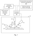
- the system includes one or more computer subsystems (e.g., computer subsystems 36 and 102) and one or more components 100 executed by the one or more computer subsystems.
- the one or more components include machine learning based model 104 configured for performing one or more simulations for specimens. As described further herein, the machine learning based model is trained with only information for nominal instances of one or more of the specimens.
- the system includes optical based imaging subsystem 10,
- the optical based imaging subsystem is configured to generate optical images of the specimens, and the one or more computer subsystems are configured for receiving the optical images from the optical based imaging subsystem.
- the optical based imaging subsystem may also be configured to generate the optical images with multiple modes.
- the specimens include wafers.
- the wafers may include any wafers known in the art.
- the specimens include reticles.
- the reticles may include any reticles known in the art.
- optical based imaging subsystem 10 may generate the optical images by directing light to or scanning light over the specimens and detecting light from the specimens.
- optical based imaging subsystem 10 includes an illumination subsystem configured to direct light to specimen 14.
- the illumination subsystem includes at least one light source.
- the illumination subsystem includes light source 16.
- the illumination subsystem is configured to direct the light to the specimen at one or more angles of incidence, which may include one or more oblique angles and/or one or more normal angles.
- light from light source 16 is directed through optical element 18 and then lens 20 to specimen 14 at an oblique angle of incidence.
- the oblique afigle of incidence may include any suitable oblique angle of incidence, which may vary depending on, for instance, characteristics of the specimen.
- the optical based imaging subsystem may be configured to direct the light to the specimen at different angles of incidence at different times.
- the optical based imaging subsystem may be configured to alter one or more characteristics of one or more elements of the illumination subsystem such that the light can be directed to the specimen at an angle of incidence that is different than that shown in Fig. 1 .
- the optical based imaging subsystem may be configured to move light source 16, optical element 18, and lens 20 such that the light is directed to the specimen at a different oblique angle of incidence or a normal (or near normal) angle of incidence.
- the optical based imaging subsystem may be configured to direct light to the specimen at more than one angle of incidence at the same time.
- the illumination subsystem may include more than one illumination channel, one of the illumination channels may include light source 16, optical element 18, and lens 20 as shown in Fig. 1 and another of the illumination channels (not shown) may include similar elements, which may be configured differently or the same, or may include at least a light source and possibly one or more other components such as those described further herein.
- one or more characteristics e.g, wavelength, polarization, etc.
- characteristics of the light directed to the specimen at different angles of incidence may be different such that light resulting from illumination of the specimen at the different angles of incidence can be discriminated from each other at the detector(s).
- the illumination subsystem may include only one light source (e.g., source 16 shown in Fig. 1 ) and light from the light source may be separated into different optical paths (e.g, based on wavelength, polarization, etc.) by one or more optical elements (not shown) of the illumination subsystem. Light in each of the different optical paths may then be directed to the specimen.
- Multiple illumination channels may be configured to direct light to the specimen at the same time or at different times (e.g., when different illumination channels are used to sequentially illuminate the specimen). In another instance, the same illumination channel may be configured to direct light to the specimen with different characteristics at different times.
- optical element 18 may be configured as a spectral filter and the properties of the spectral filter can be changed in a variety of different ways (e.g., by swapping out the spectral filter) such that different wavelengths of light can be directed to the specimen at different times.
- the illumination subsystem may have any other suitable configuration known in the art for directing the light having different or the same characteristics to the specimen at different or the same angles of incidence sequentially or simultaneously.
- light source 16 may include a broadband plasma (BBP) light source.
- BBP broadband plasma
- the light source may include any other suitable light source such as a laser.
- the laser may include any suitable laser known in the art and may be configured to generate light at any suitable wavelength or wavelengths known in the art.
- the laser may be configured to generate light that is monochromatic or nearly-monochromatic. In this manner, the laser may be a narrowband laser.
- the light source may also include a polychromatic light source that generates light at multiple discrete wavelengths or wavebands.
- Lens 20 Light from optical element 18 may be focused onto specimen 14 by lens 20.
- lens 20 is shown in Fig. 1 as a single refractive optical element, it is to be understood that, in practice, lens 20 may include a number of refractive and/or reflective optical elements that in combination focus the light from the optical element to the specimen.
- the illumination subsystem shown in Fig. 1 and described herein may include any other suitable optical elements (not shown). Examples of such optical elements include, but are not limited to, polarizing component(s), spectral filter(s), spatial filter(s), reflective optical element(s), apodizer(s), beam splitter(s), aperture(s), and the like, which may include any such suitable optical elements known in the art.
- the optical based imaging subsystem may be configured to alter one or more of the elements of the illumination subsystem based on the type of illumination to be used for imaging.
- the optical based imaging subsystem may also include a scanning subsystem configured to cause the light to be scanned over the specimen.
- the optical based imaging subsystem may include stage 22 on which specimen 14 is disposed during imaging.
- the scanning subsystem may include any suitable mechanical and/or robotic assembly (that includes stage 22) that can be configured to move the specimen such that the light can be scanned over the specimen.
- the optical based imaging subsystem may be configured such that one or more optical elements of the optical based imaging subsystem perform some scanning of the light over the specimen. The light may be scanned over the specimen in any suitable fashion stich as in a serpentine-like path or in a spiral path.
- the optical based imaging subsystem further includes one or more detection channels. At least one of the one or more detection channels includes a detector configured to detect light from the specimen due to illumination of the specimen by the system and to generate output responsive to the detected light.
- the optical based imaging subsystem shown in Fig. 1 includes two detection channels, one formed by collector 24, element 26, and detector 28 and another formed by collector 30, element 32, and detector 34. As shown in Fig. 1 , the two detection channels are configured to collect and detect light at different angles of collection. In some instances, both detection channels are configured to detect scattered light, and the detection channels are configured to detect light that is scattered at different angles from the specimen. However, one or more of the detection channels may be configured to detect another type of light from the specimen (e.g., reflected light).
- both detection channels are shown positioned in the plane of the paper and the illumination subsystem is also shown positioned in the plane of the paper. Therefore, in this embodiment, both detection channels are positioned in (e.g., centered in) the plane of incidence. However, one or more of the detection channels may be positioned out of the plane of incidence.
- the detection channel formed by collector 30, element 32, and detector 34 may be configured to collect and detect light that is scattered out of the plane of incidence. Therefore, such a detection channel may be commonly referred to as a "side" channel, and such a side channel may be centered in a plane that is substantially perpendicular to the plane of incidence.
- the optical based imaging subsystem may include a different number of detection channels (e.g., only one detection channel or two or more detection channels).
- the detection channel formed by collector 30, element 32, and detector 34 may form one side channel as described above, and the optical based imaging subsystem may include an additional detection channel (not shown) formed as another side channel that is positioned on the opposite side of the plane of incidence. Therefore, the optical based imaging subsystem may include the detection channel that includes collector 24, element 26, and detector 28 and that is centered in the plane of incidence and configured to collect and detect light at scattering angle(s) that are at or close to normal to the specimen surface.
- This detection channel may therefore be commonly referred to as a "top" channel and the optical based imaging subsystem may also include two or more side channels configured as described above.
- the optical based imaging subsystem may include at least three channels (i.e,, one top channel and two side channels), and each of the at least three channels has its own collector, each of which is configured to collect light at different scattering angles than each of the other collectors.
- each of the detection channels included in the optical based imaging subsystem may be configured to detect scattered light. Therefore, the optical based imaging subsystem shown in Fig. 1 may be configured for dark field (DF) imaging of specimens. However, the optical based imaging subsystem may also or alternatively include detection channel(s) that are configured for bright field (HF) imaging of specimens. In other words, the optical based imaging subsystem may include at least one detection channel that is configured to detect light specularly reflected from the specimen. Therefore, the optical based imaging subsystems described herein may be configured for only IDF, only BF, or both DF and BF imaging. Although each of the collectors are shown in Fig. 1 as single refractive optical elements, it is to be understood that each of the collectors may include one or more refractive optical element(s) and/or one or more reflective optical element(s).
- the one or more detection channels may include any suitable detectors known in the art.
- the detectors may include photo-multiplier tubes (PMTs), charge coupled devices (CCDs), time delay integration (TDI) cameras, and any other suitable detectors known in the art.
- the detectors may also include non-imaging detectors or imaging detectors. In this manner, if the detectors are non-imaging detectors, each of the detectors may be configured to detect certain characteristics of the scattered light such as intensity but may not be configured to detect such characteristics as a function of position within the imaging plane.
- the output that is generated by each of the detectors included in each of the detection channels of the optical based imaging subsystem may be signals or data, but not image signals or image data.
- a computer subsystem such as computer subsystem 36 may be configured to generate images of the specimen from the non-imaging output of the detectors.
- the detectors may be configured as imaging detectors that are configured to generate imaging signals or image data. Therefore, the optical based imaging subsystem may be configured to generate the optical images described herein in a number of ways,
- Fig. 1 is provided herein to generally illustrate a configuration of an optical based imaging subsystem that may be included in the system embodiments described herein or that may generate images that are used by the system embodiments described herein.
- the optical based imaging subsystem configuration described herein may be altered to optimize the performance of the optical based imaging subsystem as is normally performed when designing a commercial imaging system.
- the systems described herein may be implemented using an existing system ⁇ e.g., by adding functionality described herein to an existing system) such as the 29xx/28xx series of tools that are commercially available from KLA-Tencor, Milpitas, Calif.
- the embodiments described herein may be provided as optional functionality of the system (e.g., in addition to other functionality of the system).
- the optical based imaging subsystem described herein may be designed "from scratch" to provide a completely new optical based imaging subsystem.
- Computer subsystem 36 coupled to the optical based imaging subsystem may be coupled to the detectors of the optical based imaging subsystem in any suitable manner (e.g., via one or more transmission media, which may include "wired” and/or “wireless” transmission media) such that the computer subsystem can receive the output generated by the detectors for the specimen.
- Computer subsystem 36 may be configured to perform a number of functions described further herein using the output of the detectors.
- the computer subsystems shown in Fig. 1 may also be referred to herein as computer system(s).
- Each of the computer subsystem(s) or system(s) described herein may take various forms, including a personal computer system, image computer, mainframe computer system, workstation, network appliance, Internet appliance, or other device.
- the term "computer system” may be broadly defined to encompass any device having one or more processors, which executes instructions from a memory medium.
- the computer subsystem(s) or system(s) may also include any suitable processor known in the art such as a parallel processor.
- the computer subsystem(s) or system(s) may include a computer platform with high speed processing and software, either as a standalone or a networked tool.
- computer subsystem 36 may be coupled to computer subsystem(s) 102 as shown by the dashed line in Fig. 1 by any suitable transmission media, which may include any suitable wired and/or wireless transmission media known in the art. Two or more of such computer subsystems may also be effectively coupled by a shared computer-readable storage medium (not shown).
- the imaging subsystem may also or alternatively include an electron beam based imaging subsystem configured to generate electron beam images of the specimens, and the one or more computer subsystems are configured for receiving the electron beam images from the electron beam based imaging subsystem.
- the electron beam based imaging subsystem may be configured to direct electrons to or scan electrons over the specimen and to detect electrons from the specimen.
- the electron beam based imaging subsystem includes electron column 122 coupled to computer subsystem 124.
- the electron column includes electron beam source 126 configured to generate electrons that are focused to specimen 128 by one or more elements 130.
- the electron beam source may include, for example, a cathode source or emitter tip, and one or more elements 130 may include, for example, a gun lens, an anode, a beam limiting aperture, a gate valve, a beam current selection aperture, an objective lens, and a scanning subsystem, all of which may include any such suitable elements known in the art.
- Electrons returned from the specimen may be focused by one or more elements 132 to detector 134.
- One or more elements 132 may include, for example, a scanning subsystem, which may be the same scanning subsystem included in element(s) 130.
- the electron column may include any other suitable elements known in the art.
- An example of an electron column configuration is described in U.S. Patent Nos. 8,664,594 issued April 4, 2014 to Jiang et al. , 8,692,204 issued April 8, 2014 to Kojima et al. , 8,698,093 issued April 15, 2014 to Gubbens et al. , and 8,716,662 issued May 6, 2014 to MacDonald et al. .
- the electron column is shown in Fig. 1a as being configured such that the electrons are directed to the specimen at an oblique angle of incidence and are scattered from the specimen at another oblique angle, it is to be understood that the electron beam may be directed to and scattered from the specimen at any suitable angles.
- the electron beam based imaging subsystem may be configured to use multiple modes to generate images of the specimen as described further herein (e.g., with different illumination angles, collection angles, etc.). The multiple modes of the electron beam based imaging subsystem may be different in any image generation parameters of the electron beam based imaging subsystem.
- Computer subsystem 124 may be coupled to detector 134 as described above, The detector may detect electrons returned from the surface of the specimen thereby forming electron beam images of the specimen.
- the electron beam images may include any suitable electron beam images.
- Computer subsystem 124 may be configured to perform one or more, functions described further herein for the specimen using output generated by detector 134.
- Computer subsystem 124 may be configured to perform any additional step(s) described herein.
- a system that includes the electron beam based imaging subsystem shown in Fig. 1a may be further configured as described herein.
- Fig. 1a is provided herein to generally illustrate a configuration of an electron beam based imaging subsystem that may be included in the embodiments described herein.
- the electron beam based imaging subsystem configuration described herein may be altered to optimize the performance of the imaging subsystem as is normally performed when designing a commercial imaging subsystern.
- the systems described herein may be implemented using an existing system (e.g. by adding functionality described herein to an existing system) such as the eSxxx and eDR-xxxx series of tools that are commercially available from KLA-Tencor.
- the embodiments described herein may be provided as optional functionality of the system (e.g, in addition to other functionality of the system).
- the system described herein may be designed "from scratch" to provide a completely new system.
- the imaging subsystem may be an ion beam based imaging subsystem.
- Such an imaging subsystem may be configured as shown in Fig. 1a except that the electron beam source may be replaced with any suitable ion beam source known in the art.
- the imaging subsystem may be any other suitable ion beam-based imaging subsystem such as those included in commercially available focused ion beam (FIB) systems, helium ion microscopy (HIM) systems, and secondary ion mass spectroscopy (SIMS) systems.
- FIB focused ion beam
- HIM helium ion microscopy
- SIMS secondary ion mass spectroscopy
- the optical and electron beam based imaging subsystems may be configured for directing energy (e.g., light, electrons) to and/or scanning energy over a physical version of the specimen thereby generating actual images for the physical version of the specimen.
- energy e.g., light, electrons
- the optical and electron beam based imaging subsystems may be configured as "actual" imaging systems, rather than “virtual” systems.
- a storage medium (not shown) and computer subsystem(s) 102 shown in Fig. 1 may be configured as a "virtual" system.
- the storage medium and the computer subsystem(s) are not part of imaging subsystem 10 and do not have any capability for handling the physical version of the specimen.
- the output of its one or more "detectors” may be output that was previously generated by one or more detectors of an actual system and that is stored in the virtual system, and during the "imaging and/or scanning," the virtual system may replay the stored output as though the specimen is being imaged and/or scanned.
- imaging and/or scanning the specimen with a virtual system may appear to be the same as though a physical specimen is being imaged and/or scanned with an actual system, while, in reality, the "imaging and/or scanning” involves simply replaying output for the specimen in the same manner as the specimen may be imaged and/or scanned.
- Systems and methods configured as "virtual" inspection systems are described in commonly assigned U.S. Patent Nos. 8,126,255 issued on February 28, 2012 to Bhaskar et al. and 9,222,895 issued on December 29, 2015 to Duffy et al. .
- the imaging subsystem may be configured to generate images of the specimen with multiple modes.
- a "mode" can be defined by the values of parameters of the imaging subsystem used for generating images of a specimen or the output used to generate images of the specimen. Therefore, modes that are different may be different in the values for at least one of the imaging parameters of the imaging subsystem.
- at least one of the multiple modes uses at least one wavelength of the light for illumination that is different from at least one wavelength of the light for illumination used for at least one other of the multiple modes.
- the modes may be different in the illumination wavelength as described further herein (e.g., by using different light sources, different spectral filters, etc.) for different modes.
- At least one of the multiple modes uses an illumination channel of the imaging subsystem that is different from an illumination channel of the imaging subsystem used for at least one other of the multiple modes.
- the imaging subsystem may include more than one illumination channel. As such, different illumination channels may be used for different modes.
- the system includes an inspection subsystem configured to generate output for the specimens, and the one or more computer subsystems are configured for receiving the output from the inspection subsystem and detecting defects on the specimens based on the output.
- the optical and electron beam imaging subsystems described herein may be configured as inspection subsystems.
- the computer subsystem(s) may be configured to receive the output from the inspection subsystem as described above (e.g., from detector(s) of the imaging subsystem) and may be configured to detect defects on the specimens based on the output in any suitable manner.
- the computer subsystem(s) may be configured to compare the output to one or more thresholds, any output that is above the one or more thresholds may be identified by the computer subsystem(s) as defects or potential defects, and any output that is not above the one or more thresholds may be identified by the computer subsystem(s) as not defects or not potential defects
- the computer subsystem(s) may be configured to use any suitable algorithm(s) and/or method(s) to detect defects on the specimens based on the output.
- the system includes a defect review subsystem configured to generate output for defects detected on the specimen, and the computer subsystem(s) are configured for receiving the output from the defect review subsystem and determining properties of the defects detected on the specimens based on the output.
- the optical and electron beam imaging subsystems described herein may be configured as defect review subsystems.
- the computer subsystem(s) may be configured to receive the output from the defect review subsystem as described above (e.g., from detector(s) of the imaging subsystem) and may be configured to determine properties of the defects on the specimens based on the output in any suitable manner.
- the computer subsystem(s) may be configured to use the output to determine one or more properties such as size and shape of the defects using any suitable algorithm(s) and/or method(s) known in the art.
- the system includes a metrology subsystem configured to generate output for the specimens, and the one or more computer subsystems are configured for receiving the output from the metrology subsystem and determining properties of the specimens based on the output.
- the optical and electron beam imaging subsystems described herein may be configured as metrology subsystems.
- the computer subsystem(s) may be configured to receive the output from the metrology subsystem as described above (e.g., from detector(s) of the imaging subsystem) and may be configured to determine properties of the specimens based on the output in any suitable manner.
- the computer subsystem(s) may be configured to use the output to determine one or more properties such as size and shape of the patterned features formed on the specimens using any suitable algorithm(s) and/or method(s) known in the art.
- the embodiments of the imaging subsystems described herein and shown in Figs. 1 and 1a may be modified in one or more parameters to provide different imaging capability depending on the application for which they will be used.
- the imaging subsystem shown in Fig. 1 may be configured to have a higher resolution if it is to be used for defect review or metrology rather than for inspection.
- the embodiments of the imaging subsystem shown in Figs. 1 and 1a describe some general and various configurations for an imaging subsystem that can be tailored in a number of manners that will be obvious to one skilled in the art to produce imaging subsystems having different imaging capabilities that are more or less suitable for different applications.
- the inspection subsystem, defect review subsystem, and metrology subsystem may also be configured for inspection, defect review, and metrology of specimens such as wafers and reticles.
- the embodiments described herein are configured for training a machine learning based model that performs one or more simulations for the purposes of mask inspection, wafer inspection, and wafer metrology.
- the embodiments described herein may be installed on a computer node or computer cluster that is a component of or coupled to an imaging subsystem such as a broadband plasma inspector, an electron beam inspector or defect review tool, a mask inspector, a virtual inspector, etc.
- the embodiments described herein may perform simulations that can be used for a variety of applications that include, but are not limited to, wafer inspection, mask inspection, electron beam inspection and review, metrology, etc.
- the characteristics of the imaging subsystems shown in Figs. 1 and 1a can be modified as described above based on the specimen for which it will generate actual images.
- the system includes a semiconductor fabrication subsystem configured to perform one or more fabrication processes on the specimen.
- the system may include semiconductor fabrication subsystem 106, which may be coupled to computer subsystem(s) 102 and/or any other elements of the system described herein.
- the semiconductor fabrication subsystem may include any semiconductor fabrication tool and/or chamber known in the art such as a lithography track, an etch chamber, a chemical mechanical polishing (CMP) tool, a deposition chamber, a stripping or cleaning chamber, and the like. Examples of suitable semiconductor fabrication tools are described in U.S. Patent No. 6,891,627 to Levy et al. issued on May 10, 2005 .
- the one or more computer subsystems described herein may be included in a system with one or more other subsystems with actual wafer handling and/or processing capability (e.g., imaging subsystems, inspection subsystems, defect review subsystems, metrology subsystems, semiconductor fabrication process subsystems).
- the embodiments described herein may be configured as predictive systems including data in situ inside any semiconductor platform such as a metrology tool, an inspection tool, an etch chamber, etc. that has detector(s) and a computational platform to learn a model of its world (e.g., defects on a wafer in the case of a semiconductor inspector).
- the one or more computer subsystems described herein may be included in a system that does not include one or more subsystems that have actual wafer handling and/or processing capability.
- the embodiments described herein may be configured as a predictive system that includes data ex situ where the data is exported to a persistent storage mechanism.
- the system may be configured as a virtual system as described further herein that may or may not acquire information from actual physical wafers generated by other systems and/or methods.
- another system or method may generate information for nominal and/or non-nominal instances of one or more specimens using actual physical specimens and may store that information in a storage medium.
- the one or more computer subsystems described herein may then acquire such information from the storage medium.
- the machine learning based model is configured for performing one or more simulations for specimens, and the machine learning based model is trained with only information for nominal instances of one or more of the specimens, The training with only the nominal instances of the one or more specimens is considered as a kind of initial training that is followed by the re-training described further herein. For example, prior to being capable of giving a prediction, such a machine learning based model typically will need to be trained after it has been given a set of examples to learn from.
- Training the machine learning based model with only the nominal instances may be performed by the one or more computer subsystems described herein. However, training the machine learning based model with only the nominal instances may be performed by another system or method, and the trained machine learning based model may be acquired from the other system or method (or a storage medium in which the trained machine learning based model has been stored by the other system or method) and then re-trained by the computer subsystem(s) described herein.
- Machine learning can be generally defined as a type of artificial intelligence (AI) that provides computers with the ability to learn without being explicitly programmed.
- AI artificial intelligence
- Machine learning focuses on the development of computer programs that can teach themselves to grow and change when exposed to new data.
- machine learning can be defined as the subfield of computer science that "gives computers the ability to learn without being explicitly programmed.”
- Machine learning explores the study and construction of algorithms that can learn from and make predictions on data - such algorithms overcome following strictly static program instructions by making data driven predictions or decisions, through building a model from sample inputs.
- the one or more nominal instances of the specimens and the training performed using the one or more nominal instances may vary depending on the simulations that will be performed by the machine learning based model and the machine learning based model itself. For example, if the machine learning based model will be used to perform simulations of how the specimens will appear in images of the specimens generated by an imaging system, then the nominal instances of the specimen(s) may include design data for the specimen(s) as well as actual images generated of the specimen(s) on which the design data is printed.
- the training may then involve providing the nominal instances to the machine learning based model such that the machine learning based model can find (i.e., learn or identify) one or more parameters of the machine learning based model (e.g., weights) that cause the machine learning based model to produce simulated images from the corresponding design information that are substantially the same as the corresponding actual images.
- parameters of the machine learning based model e.g., weights
- Other types of information may be included in the information for the nominal instances used for training the machine learning based model depending on other simulations described herein (e.g., metrology system output and/or measurements with corresponding specimen design information).
- the characteristics of the information for the nominal instances may vary depending on the machine learning based model itself in that different types of machine learning based models (such as those described further herein) may require different amounts of information for training (e.g, different numbers of nominal instances).
- the characteristics of the information for the nominal instances needed for adequate training of any particular machine learning based model can be determined in any suitable manner known in the art.
- Nominal instances as that term is used herein is generally defined as "instances" of specimens on which no defects are known to be present.
- the specimen(s) that are nominal may be processed with one or more parameters of one or more processes used to form a design on the specimen(s) that are known to generate non-defective specimens.
- the process(es) used to generate the specimen(s) may be known good process(es).
- the "nominal instances" of the specimen(s) may include instances (e.g., locations on specimens, whole specimens, etc.) at which no defects have been determined to be present.
- the nominal instances of the specimen(s) may include, locations and/or specimens at which an inspection or other quality control related process (e,g., defect review metrology, etc.) have not detected any defects.
- the "non-nominal instances" of the specimen(s) as that term is used herein is generally defined as "instances" of the specimen(s) that are “defective” in some manner, either intentionally (via programmed or synthetic defects as described further herein) or unintentionally (via defects discovered on one or more specimens by inspection, defect review, metrology, etc.).
- a specimen may be “defective” even if no "defects" per se are detected on the specimen.
- a specimen may be considered “defective” if one or more measurements indicate that one or more characteristics of a design formed on the specimen are outside of a desired range of values for those one or more characteristics.
- performing the one or more simulations includes generating one or more simulated images for one of the specimens, and the one or more simulated images illustrate how the one of the specimens appears in one or more actual images of the one or more specimens generated by an imaging system.
- the one or more simulations performed by the machine learning based model may generate simulated image(s) illustrating how a specimen appears in actual image(s) generated by one of the imaging systems described herein.
- the simulated image(s) may represent images that may be generated of the specimens by an inspection system, a defect review system, or other imaging system described herein.
- the input to the one or more simulations performed by the machine learning based model may include design information for a specimen (e.g., any of the design data described further herein) and the output of the one or more simulations may include one or more simulated optical or electron beam images illustrating how the specimen on which the design information has been formed will appear in those images.
- design information for a specimen e.g., any of the design data described further herein
- the output of the one or more simulations may include one or more simulated optical or electron beam images illustrating how the specimen on which the design information has been formed will appear in those images.
- the imaging system is an optical based imaging system. In another such embodiment, the imaging system is an electron beam based imaging system. These imaging systems may be configured as described further herein.
- the one or more simulations performed by the machine learning based model may be performed to generate one or more reference images that is/are used for inspection of specimen(s). In this manner, the embodiments described herein can enable advanced inspection algorithms such as die-to-database defect detection methods and/or algorithms in a manner that are extraordinarily efficient to apply in research and development and manufacturing scenarios. Enabling such defect detection is particularly valuable for electron beam based inspection where throughput is constrained by the rate of area coverage.
- performing the one or more simulations includes generating one or more simulated measurements for one of the specimens, and the one or more simulated measurements represent output generated for the one of the specimens by a metrology system.
- the one or more simulations performed by the machine learning based model may generate simulated measurement(s) (e.g., image(s), output, data, etc.) representing output generated by one of the systems described herein for specimen(s).
- the simulated measurement(s) may represent measurements, images, output, data, etc. that may be generated for the specimens by a metrology system described herein.
- the input to the one or more simulations performed by the machine learning based model may include design information for a specimen (e.g., any of the design data described further herein) and the output of the one or more simulations may include one or more simulated optical or electron beam measurements representing output generated for the specimen by those systems.
- the computer subsystem(s) are configured for acquiring information for non-nominal instances of one or more of the specimens on which a process is performed.
- the information for the non-nominal instances will be used for re-training of the machine learning based model thereby performing transfer learning of the non-nominal instances to the machine learning based model. Therefore, acquiring the information for the non-nominal instances may essentially be transfer learning training input generation.
- Transfer learning training input generation can be performed in a number of ways described further herein including: a) empirical simulation of real defect events on wafers and masks using process design of experiments (DOEs); b) introduction of virtual defect events in design/simulation space by using synthetic approaches; and c) hybrid approaches using empirical plus synthetic methods in concert. In this manner, the embodiments described herein may use process DOEs, simulation and programmed defects to generate training sets for neural networks and other machine learning based models described herein.
- DOEs process design of experiments
- Acquiring the information for the non-nominal instances of the specimen(s) may include generating the information.
- the systems described herein may be configured to generate the information for the non-nominal instances by performing one or more processes on actual specimens (e.g., performing one or more fabrication processes on an actual, physical specimen and then performing one or more measurement and/or imaging processes on the actual physical specimen). Therefore, generating the information for the non-nominal instances may be performed using the computer subsystem(s) described herein with one or more other subsystems described herein (e.g., one or more semiconductor fabrication subsystems, one or more imaging subsystems, one or more metrology subsystems, etc.).
- the systems described herein may be configured to generate the information for the non-nominal instances by performing one or more simulations (with or without using actual, physical specimens).
- the one or more computer subsystems may be configured to use another model to generate the information for the non-nominal instances of the specimen(s).
- the embodiments described herein may be configured to acquire the information for the non-nominal instances of the specimens from a storage medium in which the information has been stored by one or more other methods and/or systems that generated the information.
- the non-nominal instances include instances of defects on the one or more specimens.
- the information for the non-nominal instances may include information for one or more defects on one or more specimens. Such information may be generated in a variety of ways described further herein.
- the non-nominal instances include instances of defects on the one or more specimens
- the one or more specimens include one or more actual specimens on which the process is performed with two or more different values of one or more parameters of the process.
- transfer learning training input generation that includes empirical simulation of real defect events on wafers and reticles using DOEs
- real world wafers can be leveraged for defects as described further herein,
- the process is performed with the two or more different values of the one or more parameters of the process in a process window qualification (PWQ) method.
- PWQ process window qualification
- one strategy for generating the transfer learning training input is to use DOEs such as PWQ as a generator of systematic defects.
- the one or more parameters of the process that are varied in the PWQ method may include focus and exposure (e.g., as in a focus-exposure PWQ process). Examples of PWQ methods are described in U.S. Patent Nos. 6,902,855 to Peterson et al. issued on June 7, 2005 , 7,418,124 to Peterson et al. issued on August 26, 2008 , 7,729,529 to Wu et al.
- the process is performed with the two or more different values of the one or more parameters of the process in a PWQ method designed for overlay margin determination.
- a PWQ method designed for overlay margin determination For example, one strategy for generating the transfer learning training input is to use DOEs such as overlay-PWQ wafers as a generator of systematic defects. Overlay margin determination may be performed in any suitable manner including as described in the above-referenced patents. Therefore, an overlay-PWQ method may be used to print such dies on a specimen, and the non-nominal instances may include instances of any defects detected on such a specimen.
- the process is performed with the two or more different values of the one or more parameters of the process in a focus exposure matrix (FEM) method.
- FEM focus exposure matrix
- one strategy for generating the transfer learning training input is to use DOEs such as FEM methods and/or wafers as a generator of systematic defects.
- FEM methods generally involve printing a number of dies on a wafer at different combinations of focus and exposure parameter values of a lithography process. The different dies can then be inspected in any suitable manner to detect defects in the different dies. That information is then typically used to determine a process window for the focus and exposure of the lithography process. Therefore, a FEM method may be used to print such dies on a specimen, and the non-nominal instances may include instances of any defects detected on such a specimen.
- the transfer learning training input generation may use one or more DOEs such as one or more of PWQ, FEM, and overlay-PWQ wafers as generators of systematic defects.
- the machine learning based model may be trained by using information generated from a PWQ or FEM wafer that can act as a generator of systematic defects.
- PWQ is a technique invented by KLA-Tencer in the early 2000s for lithography focus and exposure process window characterization and is widely adopted in one form or another.
- the basis for PWQ is to create an inspector compatible wafer where there are nominal dice and modulated dice next to each other in a systematic fashion to maximize signal for the inspector. Similar wafers can be made for determining overlay margins.
- PWQ and their "cousin" FEM wafers are primarily used for determining process margin today, they can be repurposed for training deep neural networks (or any other machine learning based model described herein) with real defects since they will occur in abundance on a given wafer. These wafers and the information generated from them can then be used as a set of training samples for the re-training described further herein. However, such samples may not provide a complete set of possible defects since there is no guarantee to see all defect types on such wafers. Therefore, the information generated from such wafers may be complemented with other information generated by synthetic defect generation, which may be performed in a number of different manners as described further herein.
- the acquired information is generated from synthetic design data for the one or more specimens produced by an electron design automation (EDA) tool.
- EDA electron design automation
- the embodiments described herein may have an added dimension of leveraging synthetic data generated with EDA computer sided design (CAD) tools
- the EDA tool may include any suitable commercially available EDA tool.
- one or more of the computer subsystems described herein e.g., computer subsystem(s) 102 may be configured as an EDA tool or may be a computer subsystem included in an EDA tool.
- the non-nominal instances include instances of defects on the one or more specimens, and the defects include one or more synthetic defects generated by altering a design for the one or more specimens to create the synthetic defects in the design.
- "Synthetic" defects as that term is used herein can be generally defined as one or more defects purposefully caused on a specimen, e.g., by manipulation of the design information for the specimen. Therefore, “synthetic" defects may also be referred to as “hypothetical” defects or "programmed” defects.
- CAD design can be used to synthetically generate defects (e.g., opens, shorts, protrusions, line ends, metrology markers, etc.) and then be treated by a deep generative or other model as described further herein (to create realistic defects on training images) and/or be used to print the synthetically generated defects on one or more specimens, which can then be used to generate images of the synthetically generated defects on the specimen(s).
- defects e.g., opens, shorts, protrusions, line ends, metrology markers, etc.
- a deep generative or other model as described further herein (to create realistic defects on training images) and/or be used to print the synthetically generated defects on one or more specimens, which can then be used to generate images of the synthetically generated defects on the specimen(s).
- the CAD work can be automated with a programmable/graphical EDA editor, which may include any suitable EDA software, hardware, system, or method.
- the one or more components include an inception module configured for altering the design to create the synthetic defects in the design.
- the machine learning based models described herein may be trained by a defect hallucination system such as those suggested by GoogLeNet inception for natural scene images.
- a traditional neural network that is pre-trained on defects can then play these backwards to create new defect types on other geometry structures. Examples of systems and methods for performing GoogLeNet inception can be found in " Going Deeper with Convolutions," Szegedy et al., 2015 IEEE Conference on Computer Vision and Pattern Recognition (CVPR), June 2015, 9 pages
- the nominal instances of the one or more specimens include natural scene images
- a model created using natural scene images can be used as a starting point to fine-tune the model that is trained on semiconductor data (optical or SEM or any other non-nominal instance information described herein).
- This is an example of transfer learning where low level features learned from training on relatively large amounts of natural images aid in classifying semiconductor defect data.
- transfer learning where low level features learned from training on relatively large amounts of natural images aid in classifying semiconductor defect data.
- natural images can be used to accelerate training time on semiconductor data. This reduction in training time is achieved by using the model weights from natural images as the initialization point for the training session that uses semiconductor data. This sharing of weights between natural and semiconductor data can be achieved via any of the transfer learning described herein.
- the natural scene images used for the nominal instances may include any suitable natural scene images known in the art, including standard natural scene images.
- the nominal instances of the specimens may include non-semiconductor specimens (i.e., not wafers or reticles), while the non-nominal instances of the specimens may include semiconductor specimens (i.e., wafers and reticles). Therefore, the training and the re-training may be performed using different types of specimens.
- the nominal instances of the specimens may include images of different types of natural scenes (e.g., animals, humans, objects, etc.)
- the nominal instances of the one or more specimens comprise more than one type of data.
- the more than one type of data may be generated for the same type of specimens (e.g., only wafers or only reticles).
- the more than one type of data may be generated using different imaging types (e.g., optical and electron beam).
- imaging types e.g., optical and electron beam.
- a variety of semiconductor data may be used to accelerate the training time for a target dataset.
- data from various semiconductor data optical and SEM
- the non-nominal instances include instances of defects on the one or more specimens
- the defects include one or more synthetic defects generated by altering a design for the one or more specimens to create the synthetic defects in the design
- the information for the non-nominal instances includes output generated by an imaging or metrology system for the one or more specimens on which the synthetic defects are printed.
- an example of a transfer learning training input generation method which uses a hybrid approach involving empirical and synthetic methods in combination, may include generation of synthetic layout defects as described above in design space and determining the empirical impact of those synthetic layout defects on wafers by making masks with the modified design and processing wafers with those masks. In this manner, the machine learning based model can be trained by actual images of progranuned defects.
- the non-nominal instances include instances of defects on the one or more specimens
- the defects include one or more synthetic defects generated by altering a design for the one or more specimens to create the synthetic defects in the design
- the information for the non-nominal instances includes the altered design.
- synthetic defects in design can be consumed in isolation without feeding them to a generative mode.
- the defects created in design do not necessarily have to be legal structures as they act as examples of structures where a nominal pattern is broken for the network to learn. These synthetic defects reduce the dependency on the need for real pattern defects thereby reducing the data acquisition period which in turn accelerates model training time. In this manner, the embodiments described herein may use synthetic design defects directly (in the absence of a generative model) to reduce training time).
- the design process for transfer learning training input generation methods by and c) described above may leverage process, lithography, and tool simulation capabilities.
- the non-nominal instances include instances of defects on the one or more specimens
- the defects include one or more synthetic defects generated by altering a design for the one or more specimens to create the synthetic defects in the design
- the information for the non-nominal instances includes output of another model
- the output of the other model represents the one or more specimens on which the synthetic defects are printed.
- the non-nominal instances include instances of defects on the one or more specimens
- the defects include one or more synthetic defects generated by altering a design for the one or more specimens to create the synthetic defects in the design
- the information for the non-nominal instances includes output of another model
- the output of the other model represents output generated by a metrology system for the one or more specimens on which the synthetic defects are printed.
- an additional capability that can be applied is simulation of the metrology tool whose recipe is being developed, In this manner, defect behavior for programmed defects can be learned in one model and applied in another.
- the output of the metrology system for the one or more specimens on which the synthetic defects are printed may be generated using any suitable model of the metrology system known in the art
- the non-nominal instances include instances of defects on the one or more specimens
- the defects include one or more synthetic defects generated by altering a design for the one or more specimens to create the synthetic defects in the design
- the information for the non-nominal instances includes output of another model
- the output of the other model represents output generated by another system for the one or more specimens on which the synthetic defects are printed
- the other model is a deep generative model.
- CAD design can be used to synthetically generate defects (e.g, opens, shorts, protrusions, line ends, metrology markers, etc.) and then be treated by a deep generative model as described further herein (to create realistic defects on training images).
- defects e.g, opens, shorts, protrusions, line ends, metrology markers, etc.
- the generative model may be used to generate simulated output that represents the output generated by any of the systems described herein (e.g., a semiconductor fabrication system, an inspection system, a defect review system, a metrology system, etc.).
- a “generative” model can be generally defined as a model that is probabilistic in nature, In other words, a “generative” model is not one that performs forward simulation or rule-based approaches and, as such, a model of the physics of the processes involved in generating an actual image or output (for which a simulated image or output is being generated) is not necessary. Instead, as described further herein, the generative model can be learned (in that its parameters can be learned) based on a suitable training set of data. As described further herein, such generative models have a number of advantages for the embodiments described herein. In addition, the generative model may be configured to have a deep learning architecture in that the generative model may include multiple layers, which perform a number of algorithms or transformations. The number of layers included in the generative model may be use case dependent. For practical purposes, a suitable range of layers is from 2 layers to a few tens of layers,
- the one or more components include a deep generative model configured to create the information for the nominal instances of the one or more specimens.
- a deep generative model configured to create the information for the nominal instances of the one or more specimens.
- deep generative models that learn the joint probability distribution (mean and variance) between the SEM (image of actual wafer) and design (e.g, CAD or a vector representation of intended layout) can be used to generate the nominal instances that are used to train the machine learning based model.
- a generative model may also be used to generate other simulation results described herein for non-nominal instances of the specimen.
- a transfer learning training input dataset which includes defective images or other non-nominal instances described herein, can be used to re-train the machine learning based model.
- a machine learning based model can be pre-trained by using synthetic data that is generated by modifying design data (e.g., CAD or EDA data) used to make semiconductor wafers. Defect artifacts such as opens, shorts, protrusions, intrusions, etc. along with metrology markers such as line end pull backs could be inserted into the CAD and then fed into a generative model trained by a network described in the above-referenced patent application by Zhang et al to create realistic defects.
- a deep generative model may be used to generate the information for the non-nominal instances of the one or more specimens.
- the same deep generative model may be used to generate the information for the nominal instances of the one or more specimens.
- a deep generative model may be used for generating nominal (reference) and defective (test) images or other information described herein.
- the machine learning based model is a discriminative model.
- the embodiments may be configured to train a discriminative model.
- the discriminative model may be part of an inspection system (e.g., a light based narrow band or broad band inspector, electron beam based inspector, etc.) or other system (e.g, a metrology system, defect review system, etc.) described herein.
- the embodiments described herein may be configured to train various inspection and/or other systems for discriminative learning.
- the discriminative model may have any suitable architecture and/or configuration known in the art.
- Discriminative models also called conditional models, are a class of models used in machine learning for modeling the dependence of an unobserved variable y on an observed variable x. Within a probabilistic framework, this is done by modeling the conditional probability distribution P(y
- the machine learning based model is a neural network.
- the machine learning based model may be a deep neural network with a set of weights that model the world according to the data that it has been fed to train it.
- Neural networks can be generally defined as a computational approach which is based on a relatively large collection of neural units loosely modeling the way a biological brain solves problems with relatively large clusters of biological neurons connected by axons. Each neural unit is connected with many others, and links can be enforcing or inhibitory in their effect on the activation state of connected neural units. These systems are self-learning and trained rather than explicitly programmed and excel in areas where the solution or feature detection is difficult to express in a traditional computer program.
- Neural networks typically consist of multiple layers, and the signal path traverses from front to back.
- the goal of the neural network is to solve problems in the same way that the human brain would, although several neural networks are much more abstract.
- Modem neural network projects typically work with a few thousand to a few million neural units and millions of connections.
- the neural network may have any suitable architecture and/or configuration known in the art.
- the machine learning based model is a convolutional and deconvolution neural network.
- the embodiments described herein can take advantage of deep learning concepts such as a convolution and deconvolution neural network to solve the normally intractable representation conversion problem (e.g., rendering).
- the machine learning based model may have any convolution and deconvolution neural network configuration or architecture known in the art.
- the computer subsystem(s) are also configured for re-training the machine learning based model with information for the non-nominal instances of the one or more of the specimens thereby performing transfer learning of the information for the non-nominal instances of the one or more of the specimens to the machine learning based model.
- a general purpose of the embodiments described herein is to provide systems and methods for simulated and/or empirical inspection and/or metrology of semiconductor devices using efficiently trainable machine learning based models with a limited training set.
- a series of transfer learning methods can be used to enable and accelerate, the efficient training of machine learning based models in a principled manner. These transfer learning methods and machine learning based models can be used for numerous inspection and metrology applications.
- Transfer learning can be generally defined as the improvement of learning in a new task (or a target task) through the transfer of knowledge from a related task that has already been learned (one or more source tasks).
- training the machine learning based model with only the nominal instances involves learning the one or more source tasks, and re-training the machine learning based model with the non-nominal instances transfers the knowledge from the source tasks (the nominal instances) to the target task (the non-nominal instances).
- the agent knows nothing about a target task (or even that there will be a target task) while it is learning a source task.
- the machine learning based model knows nothing about the non-nominal instances while it is being trained with the nominal instances.
- the transfer learning described herein may be performed in any suitable manner known in the art.
- the objective is to induce a predictive model from a set of training examples.
- Transfer in inductive learning works by allowing source-task knowledge to affect the target task's inductive bias.
- the target-task inductive bias is chosen or adjusted based on the source-task knowledge. The way this is done varies depending on which inductive learning algorithm is used to learn the source and target tasks.
- Inductive transfer can be viewed as not only a way to improve learning in a standard supervised-learning task, but also as a way to offset the difficulties posed by tasks that involve relatively small datasets. That is, if there are relatively small amounts of data or class labels for a task, treating it as a target task and performing inductive transfer from a related source task can lead to more accurate models. These approaches therefore use source-task data to enhance target-task data, despite the fact that the two datasets are assumed to come from different probability distributions.
- Transfer learning is described in " Transfer Learning,” Torrey et al., Handbook of Research on Machine Learning Applications, published by IGI Global, edited by E. Soria, J. Martin, R. Magdalena, M. Martinez and A. Serrano, 2009, 22 pages , and " How transferable are features in a deep neural network?” Yosinski et al., NIPS 2014, November 6, 2014, 14 pages .
- the re-training (and training) architecture used by the embodiments described herein is preferably designed to converge to the ground truth (for validation samples) with the minimum number of samples.
- the one or more components include one or more additional components
- the re-training is performed using the one or more additional components
- the one or more additional components include a common mother network for all layers on the specimens, a grand common mother network for all layers on the specimens, an adversarial network, a deep adversarial generative network, an adversarial autoencoder, a Bayesian Neural Network, a component configured for a variational Bayesian method, a ladder network, or some combination thereof.
- the transfer learning methods may be applied to the training set(s) generated using any of the transfer learning training input generation methods described herein to train the machine learning based models.
- the ones that have a substantially high probability for working with semiconductor wafers include: using a common mother network for front end of line (FEOL), middle of line (MOL), and back end of line (BEOL) layers each; using a grand common mother network for all layers (will likely work on SEM); using an adversarial network to accelerate training; using a Bayesian Neural Network (Variational Bayes), which requires far fewer layers; and using the concept of the ladder network for training.
- FEOL front end of line
- MOL middle of line
- BEOL back end of line
- the embodiments described herein are configured for semiconductor wafer and mask inspection and other applications and accelerating training by "legally amplifying" samples. These methods are also known as semi-supervised (a few examples are available, but the vast majority are not labeled by humans or ground truth).
- the computer subsystem(s) may leverage a pre-trained system of weights using the concept of a mother network.
- the computer subsystem(s) can also use methods such as semi-supervised methods that combine Bayesian generative modeling to achieve their results in a minimum number of samples. Examples of methods are described in U.S. Patent Application Serial No. 15/176,139 to Zhang et al. filed June 7, 2016 , and " Semi-supervised Learning with Deep Generative Models," Kingma et al., NIPS 2014, October 31, 2014, pp. 1-9 .
- the computer subsystem(s) may leverage ladder networks where supervised and unsupervised learning are combined in deep neural networks.
- the computer subsystem(s) described herein may further be configured to train the machine learning based model using a deep adversarial generative network.
- a deep adversarial generative network An example is described in " Generative Adversarial Nets" Goodfellow et al., June 10, 2014, pp. 1-9 .
- the computer subsystem(s) described herein may be configured to train the machine learning based model using an adversarial autoencoder (a method that combines a variational autoencoder (VAE) and a deep generative adversarial network (DGAN)).
- VAE variational autoencoder
- DGAN deep generative adversarial network
- the computer subsystem(s) may be configured to perform Bayesian Learning.
- Bayesian Learning for Neural Networks Neal, Springer-Verlag New York, 1996, 204 pages .
- the computer subsystem(s) may also be configured to perform a variational Bayes method.
- the Variational Bayes Method in Signal Processing ⁇ m ⁇ dl, Springer-Verlag Berlin Heidelberg, 2006, 228 pages.
- the re-training includes transferring all weights of convolutional layers of the trained machine learning based method and fine tuning weights of fully connected layers of the trained machine learning based method.
- the re-training may include transferring all the weights of the convolution layers (e.g., layers 1-3) and then fine tuning the fully connected layers only.
- a machine learning based model such as those described herein may be pre-trained by a method known as transfer learning that copies the weights from the mother network for the early layers and fine tunes the latter layers where the classification specialization occurs.
- Re-training may, however, include altering any one or more trainable parameters of the machine learning based model.
- the one or more parameters of the machine learning based model that are trained by the embodiments described herein may include one or more weights for any layer of the machine learning based model that has trainable weights.
- the weights may include weights for the convolution layers but not pooling layers.
- Fig. 2 illustrates one embodiment of machine learning based model re-training that may be performed by the embodiments described herein.
- DGMs deep generative methods
- generative model 200 may be used to generate the information for the nominal instances.
- the generative model may learn the joint probability distribution (e.g., mean and variance) between an actual image of an actual wafer (e.g., a SEM image) and design (e.g, CAD or a vector representation of intended layout).
- the generative model may be configured to perform any other simulations described herein and may have any configuration described herein.
- the information for the nominal instances is used to train machine learning based model 206, which may be performed as described further herein.
- the defect induced design may be used to generate synthetic data that looks substantially similar to the real world data (such as the PWQ data and/or defect proxies designed into the structures printed on the wafers).
- design data 202 is altered as described herein to generate synthetic defects in the design data. That altered design data may be input to generative model 200 to generate information for the non-nominal instances (i.e., the synthetic defects) of the one or more specimens based on the altered design data.
- the information for the non-nominal instances generated in this manner is also provided to machine learning based model 206 for re-training of the model, which may be performed as described further herein.
- the design data and/or the altered design data may also be provided to the machine learning based model so that the design data and/or the altered design data can be used for one or more steps performed by the machine learning based model.
- actual wafer data 204 may be generated as described further herein (e.g., using PWQ and/or FEM training wafers). That actual wafer data may be provided to generative model 200, so that the actual wafer data may be used to train and/or update the generative model. That actual wafer data may also be provided to machine learning based model 206 so that re-training of the machine learning based model may be performed using the actual wafer data, which may be performed as described further herein.
- the machine learning based model described herein may be generated for specific specimens (e.g., specific wafers or reticles), processes, imaging parameters, etc.
- the machine learning based models described herein may be specimen specific, process specific, imaging parameter specific, etc.
- different machine learning based models may be generated for different wafer layers.
- different machine learning based models may be generated for different sets of imaging parameters (e.g., different imaging modes).
- Each of the different models may be generated with different training sets of data.
- Each of the different training sets of data may be generated as described further herein.
- the embodiments described herein have a number of advantages described further herein.
- the embodiments described herein can enable a 100 - 100x acceleration of achieving a trained image generation model usable for inspection and meirology applications.
- Another embodiment relates to a computer-implemented method for training a machine learning based model.
- the method includes acquiring information for non-nominal instances of one or more specimens on which a process is performed.
- a machine learning based model is configured for performing one or more simulations for the specimens, and the machine learning based model is trained with only information for nominal instances of one or more additional specimens.
- the method also includes re-training the machine learning based model with the information for the non-nominal instances of the one or more specimens thereby performing transfer learning of the information for the non-nominal instances of the one or more specimens to the machine learning based model.
- the acquiring and re-training are performed by one or more computer systems.
- One or more components are executed by the one or more computer systems, and the one or more components include the machine learning based model.
- the method may also include any other step(s) that can be performed by the system, computer system(s), and/or machine learning based models described herein.
- the computer system(s) may be configured according to any of the embodiments described herein, e.g., computer subsystem(s) 102.
- the method described above may be performed by any of the system embodiments described herein.
- An additional embodiment relates to a non-transitory computer-readable medium storing program instructions executable on one or more computer systems for performing a computer-implemented method for training a machine learning based model.
- non-transitory computer-readable medium 300 includes program instructions 302 executable on computer system(s) 304.
- the computer-implemented method may include any step(s) of any method(s) described herein.
- Program instructions 302 implementing methods such as those described herein may be stored on computer-readable medium 300.
- the computer-readable medium may be a storage medium such as a magnetic or optical disk, a magnetic tape, or any other suitable non-transitory computer-readable medium known in the art.
- the program instructions may be implemented in any of various ways, including procedure-based techniques, component-based techniques, and/or object-oriented techniques, among others.
- the program instructions may be implemented using ActiveX controls, C++ objects, JavaBeans, Microsoft Foundation Classes ("MFC"), SSE (Streaming SIMD Extension) or other technologies or methodologies, as desired.
- MFC Microsoft Foundation Classes
- SSE Streaming SIMD Extension
- Computer system(s) 304 may be configured according to any of the embodiments described herein.
Landscapes
- Engineering & Computer Science (AREA)
- Physics & Mathematics (AREA)
- Theoretical Computer Science (AREA)
- General Physics & Mathematics (AREA)
- Life Sciences & Earth Sciences (AREA)
- Health & Medical Sciences (AREA)
- General Health & Medical Sciences (AREA)
- Data Mining & Analysis (AREA)
- Artificial Intelligence (AREA)
- Evolutionary Computation (AREA)
- General Engineering & Computer Science (AREA)
- Software Systems (AREA)
- Computing Systems (AREA)
- Mathematical Physics (AREA)
- Computational Linguistics (AREA)
- Molecular Biology (AREA)
- Biophysics (AREA)
- Biomedical Technology (AREA)
- Manufacturing & Machinery (AREA)
- Computer Vision & Pattern Recognition (AREA)
- Immunology (AREA)
- Pathology (AREA)
- Computer Hardware Design (AREA)
- Microelectronics & Electronic Packaging (AREA)
- Chemical & Material Sciences (AREA)
- Analytical Chemistry (AREA)
- Power Engineering (AREA)
- Biochemistry (AREA)
- Probability & Statistics with Applications (AREA)
- Quality & Reliability (AREA)
- Bioinformatics & Cheminformatics (AREA)
- Bioinformatics & Computational Biology (AREA)
- Evolutionary Biology (AREA)
- Testing Or Measuring Of Semiconductors Or The Like (AREA)
- Investigating Materials By The Use Of Optical Means Adapted For Particular Applications (AREA)
- Medical Informatics (AREA)
Applications Claiming Priority (3)
| Application Number | Priority Date | Filing Date | Title |
|---|---|---|---|
| US201562273985P | 2015-12-31 | 2015-12-31 | |
| US15/394,792 US9916965B2 (en) | 2015-12-31 | 2016-12-29 | Hybrid inspectors |
| PCT/US2016/069580 WO2017117568A1 (en) | 2015-12-31 | 2016-12-30 | Accelerated training of a machine learning based model for semiconductor applications |
Publications (3)
| Publication Number | Publication Date |
|---|---|
| EP3398123A1 EP3398123A1 (en) | 2018-11-07 |
| EP3398123A4 EP3398123A4 (en) | 2019-08-28 |
| EP3398123B1 true EP3398123B1 (en) | 2025-03-12 |
Family
ID=59225974
Family Applications (1)
| Application Number | Title | Priority Date | Filing Date |
|---|---|---|---|
| EP16882778.0A Active EP3398123B1 (en) | 2015-12-31 | 2016-12-30 | Accelerated training of a machine learning based model for semiconductor applications |
Country Status (6)
| Country | Link |
|---|---|
| EP (1) | EP3398123B1 (enExample) |
| JP (1) | JP6941103B2 (enExample) |
| KR (1) | KR102812577B1 (enExample) |
| CN (1) | CN108475351B (enExample) |
| IL (1) | IL259705B (enExample) |
| WO (1) | WO2017117568A1 (enExample) |
Families Citing this family (50)
| Publication number | Priority date | Publication date | Assignee | Title |
|---|---|---|---|---|
| JP6906058B2 (ja) * | 2017-02-24 | 2021-07-21 | エーエスエムエル ネザーランズ ビー.ブイ. | 機械学習によるプロセスモデルの決定方法 |
| WO2019173170A1 (en) * | 2018-03-05 | 2019-09-12 | Kla-Tencor Corporation | Visualization of three-dimensional semiconductor structures |
| US10677742B2 (en) * | 2018-03-09 | 2020-06-09 | Kla-Tencor Corp. | Detecting die repeating programmed defects located in backgrounds with non-repeating features |
| US10795346B2 (en) | 2018-03-13 | 2020-10-06 | Applied Materials, Inc. | Machine learning systems for monitoring of semiconductor processing |
| US10789703B2 (en) * | 2018-03-19 | 2020-09-29 | Kla-Tencor Corporation | Semi-supervised anomaly detection in scanning electron microscope images |
| DE102018207882A1 (de) | 2018-05-18 | 2019-11-21 | Carl Zeiss Smt Gmbh | Vorrichtung und Verfahren zur Analyse eines Elements eines Photolithographieprozesses mit Hilfe eines Transformationsmodells |
| DE102018207880A1 (de) | 2018-05-18 | 2019-11-21 | Carl Zeiss Smt Gmbh | Verfahren und Vorrichtung zum Bewerten einer unbekannten Auswirkung von Defekten eines Elements eines Photolithographieprozesses |
| DE102018209562B3 (de) | 2018-06-14 | 2019-12-12 | Carl Zeiss Smt Gmbh | Vorrichtungen und Verfahren zur Untersuchung und/oder Bearbeitung eines Elements für die Photolithographie |
| US10732130B2 (en) * | 2018-06-19 | 2020-08-04 | Kla-Tencor Corporation | Embedded particle depth binning based on multiple scattering signals |
| DE102018211099B4 (de) | 2018-07-05 | 2020-06-18 | Carl Zeiss Smt Gmbh | Verfahren und Vorrichtung zum Bewerten eines statistisch verteilten Messwertes beim Untersuchen eines Elements eines Photolithographieprozesses |
| WO2020049974A1 (ja) * | 2018-09-03 | 2020-03-12 | 株式会社Preferred Networks | 学習装置、推論装置、学習モデルの生成方法及び推論方法 |
| US10930531B2 (en) | 2018-10-09 | 2021-02-23 | Applied Materials, Inc. | Adaptive control of wafer-to-wafer variability in device performance in advanced semiconductor processes |
| US10657214B2 (en) | 2018-10-09 | 2020-05-19 | Applied Materials, Inc. | Predictive spatial digital design of experiment for advanced semiconductor process optimization and control |
| US10705514B2 (en) * | 2018-10-09 | 2020-07-07 | Applied Materials, Inc. | Adaptive chamber matching in advanced semiconductor process control |
| US20220012404A1 (en) * | 2018-12-11 | 2022-01-13 | Tasmit, Inc. | Image matching method and arithmetic system for performing image matching process |
| US11263737B2 (en) * | 2019-01-10 | 2022-03-01 | Lam Research Corporation | Defect classification and source analysis for semiconductor equipment |
| JP7570004B2 (ja) * | 2019-02-19 | 2024-10-21 | パナソニックIpマネジメント株式会社 | 研磨加工システム、学習装置、学習装置の学習方法 |
| US12124247B2 (en) | 2019-05-10 | 2024-10-22 | Sandisk Technologies Llc | Implementation of deep neural networks for testing and quality control in the production of memory devices |
| US11947890B2 (en) | 2019-05-10 | 2024-04-02 | Sandisk Technologies Llc | Implementation of deep neural networks for testing and quality control in the production of memory devices |
| WO2020232460A1 (en) * | 2019-05-14 | 2020-11-19 | Onesubsea Ip Uk Limited | Machine learning technics with system in the loop for oil & gas telemetry systems |
| US12361531B2 (en) * | 2019-05-22 | 2025-07-15 | Applied Materials Israel Ltd. | Machine learning-based classification of defects in a semiconductor specimen |
| US12293279B2 (en) | 2019-08-29 | 2025-05-06 | Synopsys, Inc. | Neural network based mask synthesis for integrated circuits |
| EP3796230B1 (en) * | 2019-09-17 | 2022-03-09 | Imec VZW | A method for determining process limits of a semiconductor process |
| CN110648935A (zh) * | 2019-09-25 | 2020-01-03 | 上海众壹云计算科技有限公司 | 一种运用ai模型的半导体制造缺陷动态随机取样方法 |
| US11341304B2 (en) * | 2019-12-10 | 2022-05-24 | Microchip Technology Inc. | Machine learning based methods and apparatus for integrated circuit design delay calculation and verification |
| US11816411B2 (en) * | 2020-01-29 | 2023-11-14 | Taiwan Semiconductor Manufacturing Co., Ltd. | Method and system for semiconductor wafer defect review |
| EP3910417A1 (en) * | 2020-05-13 | 2021-11-17 | ASML Netherlands B.V. | Method for determining an inspection strategy for a group of substrates in a semiconductor manufacturing process |
| CN115398345B (zh) * | 2020-04-02 | 2025-11-04 | Asml荷兰有限公司 | 在半导体制造过程中用于确定对于一组衬底的检查策略的方法 |
| CN115428135B (zh) | 2020-04-06 | 2024-01-26 | 诺威有限公司 | 用于基于光谱的计量和过程控制的机器和深度学习方法 |
| US12051183B2 (en) * | 2020-04-30 | 2024-07-30 | KLA Corp. | Training a machine learning model to generate higher resolution images from inspection images |
| JP7492389B2 (ja) * | 2020-07-03 | 2024-05-29 | 株式会社ホロン | 画像検査装置および画像検査方法 |
| US12321876B2 (en) * | 2020-07-21 | 2025-06-03 | UiPath, Inc. | Artificial intelligence / machine learning model drift detection and correction for robotic process automation |
| US11289387B2 (en) | 2020-07-31 | 2022-03-29 | Applied Materials, Inc. | Methods and apparatus for backside via reveal processing |
| US11328410B2 (en) | 2020-08-03 | 2022-05-10 | KLA Corp. | Deep generative models for optical or other mode selection |
| US11562476B2 (en) * | 2020-09-03 | 2023-01-24 | Applied Materials Israel Ltd. | Determination of a simulated image of a specimen |
| JP7527902B2 (ja) | 2020-09-04 | 2024-08-05 | キオクシア株式会社 | 情報処理装置 |
| JP7670959B2 (ja) * | 2021-04-13 | 2025-05-01 | 横浜ゴム株式会社 | 事前学習モデルを利用したターゲットモデル生成方法、評価データ予測方法、事前学習モデルを利用して生成されたターゲットモデルを記録したコンピュータ読取可能な記録媒体並びに事前学習モデルを利用したターゲットモデル生成方法のプログラム及び評価データ予測方法のプログラム |
| US12020418B2 (en) * | 2021-04-22 | 2024-06-25 | Taiwan Semiconductor Manufacturing Company, Ltd. | Image processing method and system, and non-transitory computer readable medium |
| WO2022233546A1 (en) * | 2021-05-06 | 2022-11-10 | Asml Netherlands B.V. | Method for determining a stochastic metric relating to a lithographic process |
| CN113344886A (zh) * | 2021-06-11 | 2021-09-03 | 长江存储科技有限责任公司 | 晶圆表面缺陷检测方法和设备 |
| JP2023005735A (ja) * | 2021-06-29 | 2023-01-18 | 株式会社アルバック | 数理モデル取得装置、推定装置、数理モデル取得方法、推定方法及びプログラム |
| KR20230013995A (ko) * | 2021-07-20 | 2023-01-27 | 삼성전자주식회사 | 공정 시뮬레이션 모델 생성 방법 및 장치 |
| WO2023033884A1 (en) * | 2021-09-02 | 2023-03-09 | Sandisk Technologies Llc | Implementation of deep neural networks for testing and quality control in the production of memory devices |
| US20230089092A1 (en) * | 2021-09-23 | 2023-03-23 | Applied Materials, Inc. | Machine learning platform for substrate processing |
| US20250003899A1 (en) * | 2021-11-12 | 2025-01-02 | Asml Netherlands B.V. | Method and system of image analysis and critical dimension matching for charged-particle inspection apparatus |
| KR20240105405A (ko) * | 2021-11-28 | 2024-07-05 | 디2에스, 인코포레이티드 | 전자 설계 자동화를 위한 상호작용적 압축 툴 |
| CN114664395B (zh) * | 2022-03-25 | 2024-11-22 | 上海交通大学 | 基于神经网络和贝叶斯优化的热辐射材料设计方法及系统 |
| JP7607767B2 (ja) * | 2022-05-20 | 2024-12-27 | 株式会社日立ハイテク | 探索装置および探索方法並びに半導体装置製造システム |
| US20240353759A1 (en) * | 2023-04-19 | 2024-10-24 | Kla Corporation | Full Wafer Measurement Based On A Trained Full Wafer Measurement Model |
| WO2025051477A1 (en) * | 2023-09-05 | 2025-03-13 | Asml Netherlands B.V. | Semi-supervised, self-supervised, and reinforcement learning machine learning models for mask prediction |
Family Cites Families (30)
| Publication number | Priority date | Publication date | Assignee | Title |
|---|---|---|---|---|
| US5212765A (en) * | 1990-08-03 | 1993-05-18 | E. I. Du Pont De Nemours & Co., Inc. | On-line training neural network system for process control |
| JP3288066B2 (ja) * | 1992-03-10 | 2002-06-04 | 富士通株式会社 | ネットワーク構成データ処理装置の学習処理方法およびシステム |
| US7167583B1 (en) | 2000-06-28 | 2007-01-23 | Landrex Technologies Co., Ltd. | Image processing system for use with inspection systems |
| US6891627B1 (en) | 2000-09-20 | 2005-05-10 | Kla-Tencor Technologies Corp. | Methods and systems for determining a critical dimension and overlay of a specimen |
| US6902855B2 (en) | 2002-07-15 | 2005-06-07 | Kla-Tencor Technologies | Qualifying patterns, patterning processes, or patterning apparatus in the fabrication of microlithographic patterns |
| US7418124B2 (en) | 2002-07-15 | 2008-08-26 | Kla-Tencor Technologies Corp. | Qualifying patterns, patterning processes, or patterning apparatus in the fabrication of microlithographic patterns |
| US20040267397A1 (en) * | 2003-06-27 | 2004-12-30 | Srinivas Doddi | Optical metrology of structures formed on semiconductor wafer using machine learning systems |
| US7729529B2 (en) | 2004-12-07 | 2010-06-01 | Kla-Tencor Technologies Corp. | Computer-implemented methods for detecting and/or sorting defects in a design pattern of a reticle |
| US7769225B2 (en) | 2005-08-02 | 2010-08-03 | Kla-Tencor Technologies Corp. | Methods and systems for detecting defects in a reticle design pattern |
| WO2007120279A2 (en) * | 2005-11-18 | 2007-10-25 | Kla-Tencor Technologies Corporation | Methods and systems for utilizing design data in combination with inspection data |
| US7676077B2 (en) | 2005-11-18 | 2010-03-09 | Kla-Tencor Technologies Corp. | Methods and systems for utilizing design data in combination with inspection data |
| US7570796B2 (en) | 2005-11-18 | 2009-08-04 | Kla-Tencor Technologies Corp. | Methods and systems for utilizing design data in combination with inspection data |
| US8102408B2 (en) * | 2006-06-29 | 2012-01-24 | Kla-Tencor Technologies Corp. | Computer-implemented methods and systems for determining different process windows for a wafer printing process for different reticle designs |
| US7792353B2 (en) * | 2006-10-31 | 2010-09-07 | Hewlett-Packard Development Company, L.P. | Retraining a machine-learning classifier using re-labeled training samples |
| US8698093B1 (en) | 2007-01-19 | 2014-04-15 | Kla-Tencor Corporation | Objective lens with deflector plates immersed in electrostatic lens field |
| US7483809B2 (en) * | 2007-04-12 | 2009-01-27 | Tokyo Electron Limited | Optical metrology using support vector machine with profile parameter inputs |
| US8213704B2 (en) | 2007-05-09 | 2012-07-03 | Kla-Tencor Corp. | Methods and systems for detecting defects in a reticle design pattern |
| US8126255B2 (en) | 2007-09-20 | 2012-02-28 | Kla-Tencor Corp. | Systems and methods for creating persistent data for a wafer and for using persistent data for inspection-related functions |
| US8041106B2 (en) | 2008-12-05 | 2011-10-18 | Kla-Tencor Corp. | Methods and systems for detecting defects on a reticle |
| US8533222B2 (en) * | 2011-01-26 | 2013-09-10 | Google Inc. | Updateable predictive analytical modeling |
| US8664594B1 (en) | 2011-04-18 | 2014-03-04 | Kla-Tencor Corporation | Electron-optical system for high-speed and high-sensitivity inspections |
| US8692204B2 (en) | 2011-04-26 | 2014-04-08 | Kla-Tencor Corporation | Apparatus and methods for electron beam detection |
| US8468471B2 (en) * | 2011-09-23 | 2013-06-18 | Kla-Tencor Corp. | Process aware metrology |
| US8570531B2 (en) * | 2011-12-11 | 2013-10-29 | Tokyo Electron Limited | Method of regenerating diffraction signals for optical metrology systems |
| US8716662B1 (en) | 2012-07-16 | 2014-05-06 | Kla-Tencor Corporation | Methods and apparatus to review defects using scanning electron microscope with multiple electron beam configurations |
| CN102937784A (zh) * | 2012-10-30 | 2013-02-20 | 中冶南方工程技术有限公司 | 基于人工神经网络的铸坯质量在线预报的控制方法 |
| US9222895B2 (en) | 2013-02-25 | 2015-12-29 | Kla-Tencor Corp. | Generalized virtual inspector |
| US10502694B2 (en) * | 2013-08-06 | 2019-12-10 | Kla-Tencor Corporation | Methods and apparatus for patterned wafer characterization |
| US20150204799A1 (en) * | 2014-01-21 | 2015-07-23 | International Business Machines Corporation | Computer-based defect root cause and yield impact determination in layered device manufacturing for products and services |
| WO2019183153A1 (en) * | 2018-03-21 | 2019-09-26 | Kla-Tencor Corporation | Training a machine learning model with synthetic images |
-
2016
- 2016-12-30 EP EP16882778.0A patent/EP3398123B1/en active Active
- 2016-12-30 KR KR1020187021817A patent/KR102812577B1/ko active Active
- 2016-12-30 JP JP2018534670A patent/JP6941103B2/ja active Active
- 2016-12-30 CN CN201680075625.1A patent/CN108475351B/zh active Active
- 2016-12-30 WO PCT/US2016/069580 patent/WO2017117568A1/en not_active Ceased
-
2018
- 2018-05-30 IL IL259705A patent/IL259705B/en unknown
Also Published As
| Publication number | Publication date |
|---|---|
| JP2019508789A (ja) | 2019-03-28 |
| KR102812577B1 (ko) | 2025-05-23 |
| KR20180090385A (ko) | 2018-08-10 |
| EP3398123A1 (en) | 2018-11-07 |
| WO2017117568A1 (en) | 2017-07-06 |
| IL259705B (en) | 2021-07-29 |
| CN108475351A (zh) | 2018-08-31 |
| JP6941103B2 (ja) | 2021-09-29 |
| IL259705A (en) | 2018-07-31 |
| EP3398123A4 (en) | 2019-08-28 |
| CN108475351B (zh) | 2022-10-04 |
Similar Documents
| Publication | Publication Date | Title |
|---|---|---|
| EP3398123B1 (en) | Accelerated training of a machine learning based model for semiconductor applications | |
| US11580375B2 (en) | Accelerated training of a machine learning based model for semiconductor applications | |
| EP3465174B1 (en) | Generating simulated images from input images for semiconductor applications | |
| US10599951B2 (en) | Training a neural network for defect detection in low resolution images | |
| EP3350654B1 (en) | Generating simulated images from design information | |
| US11580398B2 (en) | Diagnostic systems and methods for deep learning models configured for semiconductor applications | |
| US10648924B2 (en) | Generating high resolution images from low resolution images for semiconductor applications | |
| EP3397952A1 (en) | Hybrid inspectors |
Legal Events
| Date | Code | Title | Description |
|---|---|---|---|
| STAA | Information on the status of an ep patent application or granted ep patent |
Free format text: STATUS: THE INTERNATIONAL PUBLICATION HAS BEEN MADE |
|
| PUAI | Public reference made under article 153(3) epc to a published international application that has entered the european phase |
Free format text: ORIGINAL CODE: 0009012 |
|
| STAA | Information on the status of an ep patent application or granted ep patent |
Free format text: STATUS: REQUEST FOR EXAMINATION WAS MADE |
|
| 17P | Request for examination filed |
Effective date: 20180618 |
|
| AK | Designated contracting states |
Kind code of ref document: A1 Designated state(s): AL AT BE BG CH CY CZ DE DK EE ES FI FR GB GR HR HU IE IS IT LI LT LU LV MC MK MT NL NO PL PT RO RS SE SI SK SM TR |
|
| AX | Request for extension of the european patent |
Extension state: BA ME |
|
| DAV | Request for validation of the european patent (deleted) | ||
| DAX | Request for extension of the european patent (deleted) | ||
| A4 | Supplementary search report drawn up and despatched |
Effective date: 20190726 |
|
| RIC1 | Information provided on ipc code assigned before grant |
Ipc: G06N 3/04 20060101ALI20190722BHEP Ipc: G06K 9/62 20060101ALI20190722BHEP Ipc: G01N 21/95 20060101ALI20190722BHEP Ipc: G06N 3/08 20060101ALI20190722BHEP Ipc: H01L 21/66 20060101ALI20190722BHEP Ipc: G06N 99/00 20190101AFI20190722BHEP Ipc: G03F 7/20 20060101ALI20190722BHEP |
|
| STAA | Information on the status of an ep patent application or granted ep patent |
Free format text: STATUS: EXAMINATION IS IN PROGRESS |
|
| 17Q | First examination report despatched |
Effective date: 20210624 |
|
| P01 | Opt-out of the competence of the unified patent court (upc) registered |
Effective date: 20230526 |
|
| REG | Reference to a national code |
Ref country code: DE Free format text: PREVIOUS MAIN CLASS: G06N0099000000 Ref country code: DE Ref legal event code: R079 Ref document number: 602016091556 Country of ref document: DE Free format text: PREVIOUS MAIN CLASS: G06N0099000000 Ipc: G06N0003096000 |
|
| RIC1 | Information provided on ipc code assigned before grant |
Ipc: G06F 18/21 20230101ALI20240829BHEP Ipc: H01L 21/66 20060101ALI20240829BHEP Ipc: G06T 7/00 20170101ALI20240829BHEP Ipc: G03F 7/00 20060101ALI20240829BHEP Ipc: G01N 21/95 20060101ALI20240829BHEP Ipc: G06N 3/047 20230101ALI20240829BHEP Ipc: G06N 3/088 20230101ALI20240829BHEP Ipc: G06N 3/0464 20230101ALI20240829BHEP Ipc: G06N 3/0455 20230101ALI20240829BHEP Ipc: G06N 3/096 20230101AFI20240829BHEP |
|
| GRAP | Despatch of communication of intention to grant a patent |
Free format text: ORIGINAL CODE: EPIDOSNIGR1 |
|
| STAA | Information on the status of an ep patent application or granted ep patent |
Free format text: STATUS: GRANT OF PATENT IS INTENDED |
|
| INTG | Intention to grant announced |
Effective date: 20241004 |
|
| GRAS | Grant fee paid |
Free format text: ORIGINAL CODE: EPIDOSNIGR3 |
|
| GRAA | (expected) grant |
Free format text: ORIGINAL CODE: 0009210 |
|
| STAA | Information on the status of an ep patent application or granted ep patent |
Free format text: STATUS: THE PATENT HAS BEEN GRANTED |
|
| AK | Designated contracting states |
Kind code of ref document: B1 Designated state(s): AL AT BE BG CH CY CZ DE DK EE ES FI FR GB GR HR HU IE IS IT LI LT LU LV MC MK MT NL NO PL PT RO RS SE SI SK SM TR |
|
| REG | Reference to a national code |
Ref country code: GB Ref legal event code: FG4D |
|
| REG | Reference to a national code |
Ref country code: CH Ref legal event code: EP |
|
| REG | Reference to a national code |
Ref country code: DE Ref legal event code: R096 Ref document number: 602016091556 Country of ref document: DE |
|
| REG | Reference to a national code |
Ref country code: NL Ref legal event code: FP Ref country code: IE Ref legal event code: FG4D |
|
| PG25 | Lapsed in a contracting state [announced via postgrant information from national office to epo] |
Ref country code: RS Free format text: LAPSE BECAUSE OF FAILURE TO SUBMIT A TRANSLATION OF THE DESCRIPTION OR TO PAY THE FEE WITHIN THE PRESCRIBED TIME-LIMIT Effective date: 20250612 |
|
| PG25 | Lapsed in a contracting state [announced via postgrant information from national office to epo] |
Ref country code: FI Free format text: LAPSE BECAUSE OF FAILURE TO SUBMIT A TRANSLATION OF THE DESCRIPTION OR TO PAY THE FEE WITHIN THE PRESCRIBED TIME-LIMIT Effective date: 20250312 |
|
| PG25 | Lapsed in a contracting state [announced via postgrant information from national office to epo] |
Ref country code: ES Free format text: LAPSE BECAUSE OF FAILURE TO SUBMIT A TRANSLATION OF THE DESCRIPTION OR TO PAY THE FEE WITHIN THE PRESCRIBED TIME-LIMIT Effective date: 20250312 |
|
| REG | Reference to a national code |
Ref country code: LT Ref legal event code: MG9D |
|
| PG25 | Lapsed in a contracting state [announced via postgrant information from national office to epo] |
Ref country code: NO Free format text: LAPSE BECAUSE OF FAILURE TO SUBMIT A TRANSLATION OF THE DESCRIPTION OR TO PAY THE FEE WITHIN THE PRESCRIBED TIME-LIMIT Effective date: 20250612 |
|
| PG25 | Lapsed in a contracting state [announced via postgrant information from national office to epo] |
Ref country code: HR Free format text: LAPSE BECAUSE OF FAILURE TO SUBMIT A TRANSLATION OF THE DESCRIPTION OR TO PAY THE FEE WITHIN THE PRESCRIBED TIME-LIMIT Effective date: 20250312 |
|
| PG25 | Lapsed in a contracting state [announced via postgrant information from national office to epo] |
Ref country code: LV Free format text: LAPSE BECAUSE OF FAILURE TO SUBMIT A TRANSLATION OF THE DESCRIPTION OR TO PAY THE FEE WITHIN THE PRESCRIBED TIME-LIMIT Effective date: 20250312 |
|
| PG25 | Lapsed in a contracting state [announced via postgrant information from national office to epo] |
Ref country code: GR Free format text: LAPSE BECAUSE OF FAILURE TO SUBMIT A TRANSLATION OF THE DESCRIPTION OR TO PAY THE FEE WITHIN THE PRESCRIBED TIME-LIMIT Effective date: 20250613 Ref country code: BG Free format text: LAPSE BECAUSE OF FAILURE TO SUBMIT A TRANSLATION OF THE DESCRIPTION OR TO PAY THE FEE WITHIN THE PRESCRIBED TIME-LIMIT Effective date: 20250312 |
|
| REG | Reference to a national code |
Ref country code: AT Ref legal event code: MK05 Ref document number: 1775629 Country of ref document: AT Kind code of ref document: T Effective date: 20250312 |
|
| PG25 | Lapsed in a contracting state [announced via postgrant information from national office to epo] |
Ref country code: SE Free format text: LAPSE BECAUSE OF FAILURE TO SUBMIT A TRANSLATION OF THE DESCRIPTION OR TO PAY THE FEE WITHIN THE PRESCRIBED TIME-LIMIT Effective date: 20250312 |
|
| PG25 | Lapsed in a contracting state [announced via postgrant information from national office to epo] |
Ref country code: SM Free format text: LAPSE BECAUSE OF FAILURE TO SUBMIT A TRANSLATION OF THE DESCRIPTION OR TO PAY THE FEE WITHIN THE PRESCRIBED TIME-LIMIT Effective date: 20250312 |
|
| PG25 | Lapsed in a contracting state [announced via postgrant information from national office to epo] |
Ref country code: PT Free format text: LAPSE BECAUSE OF FAILURE TO SUBMIT A TRANSLATION OF THE DESCRIPTION OR TO PAY THE FEE WITHIN THE PRESCRIBED TIME-LIMIT Effective date: 20250714 |
|
| PG25 | Lapsed in a contracting state [announced via postgrant information from national office to epo] |
Ref country code: PL Free format text: LAPSE BECAUSE OF FAILURE TO SUBMIT A TRANSLATION OF THE DESCRIPTION OR TO PAY THE FEE WITHIN THE PRESCRIBED TIME-LIMIT Effective date: 20250312 Ref country code: IT Free format text: LAPSE BECAUSE OF FAILURE TO SUBMIT A TRANSLATION OF THE DESCRIPTION OR TO PAY THE FEE WITHIN THE PRESCRIBED TIME-LIMIT Effective date: 20250312 |
|
| PG25 | Lapsed in a contracting state [announced via postgrant information from national office to epo] |
Ref country code: AT Free format text: LAPSE BECAUSE OF FAILURE TO SUBMIT A TRANSLATION OF THE DESCRIPTION OR TO PAY THE FEE WITHIN THE PRESCRIBED TIME-LIMIT Effective date: 20250312 |
|
| PG25 | Lapsed in a contracting state [announced via postgrant information from national office to epo] |
Ref country code: EE Free format text: LAPSE BECAUSE OF FAILURE TO SUBMIT A TRANSLATION OF THE DESCRIPTION OR TO PAY THE FEE WITHIN THE PRESCRIBED TIME-LIMIT Effective date: 20250312 Ref country code: CZ Free format text: LAPSE BECAUSE OF FAILURE TO SUBMIT A TRANSLATION OF THE DESCRIPTION OR TO PAY THE FEE WITHIN THE PRESCRIBED TIME-LIMIT Effective date: 20250312 |
|
| PG25 | Lapsed in a contracting state [announced via postgrant information from national office to epo] |
Ref country code: RO Free format text: LAPSE BECAUSE OF FAILURE TO SUBMIT A TRANSLATION OF THE DESCRIPTION OR TO PAY THE FEE WITHIN THE PRESCRIBED TIME-LIMIT Effective date: 20250312 |
|
| PG25 | Lapsed in a contracting state [announced via postgrant information from national office to epo] |
Ref country code: SK Free format text: LAPSE BECAUSE OF FAILURE TO SUBMIT A TRANSLATION OF THE DESCRIPTION OR TO PAY THE FEE WITHIN THE PRESCRIBED TIME-LIMIT Effective date: 20250312 |
|
| PG25 | Lapsed in a contracting state [announced via postgrant information from national office to epo] |
Ref country code: IS Free format text: LAPSE BECAUSE OF FAILURE TO SUBMIT A TRANSLATION OF THE DESCRIPTION OR TO PAY THE FEE WITHIN THE PRESCRIBED TIME-LIMIT Effective date: 20250712 |