EP3391408B1 - Oxidation resistant barrier metal for semiconductor devices and corresponding process - Google Patents
Oxidation resistant barrier metal for semiconductor devices and corresponding process Download PDFInfo
- Publication number
- EP3391408B1 EP3391408B1 EP16876903.2A EP16876903A EP3391408B1 EP 3391408 B1 EP3391408 B1 EP 3391408B1 EP 16876903 A EP16876903 A EP 16876903A EP 3391408 B1 EP3391408 B1 EP 3391408B1
- Authority
- EP
- European Patent Office
- Prior art keywords
- layer
- barrier layer
- oxidation resistant
- resistant barrier
- geometry
- Prior art date
- Legal status (The legal status is an assumption and is not a legal conclusion. Google has not performed a legal analysis and makes no representation as to the accuracy of the status listed.)
- Active
Links
- 229910052751 metal Inorganic materials 0.000 title claims description 88
- 239000002184 metal Substances 0.000 title claims description 88
- 230000004888 barrier function Effects 0.000 title claims description 72
- 230000003647 oxidation Effects 0.000 title claims description 40
- 238000007254 oxidation reaction Methods 0.000 title claims description 40
- 238000000034 method Methods 0.000 title claims description 23
- 239000004065 semiconductor Substances 0.000 title 1
- IJGRMHOSHXDMSA-UHFFFAOYSA-N Atomic nitrogen Chemical compound N#N IJGRMHOSHXDMSA-UHFFFAOYSA-N 0.000 claims description 58
- 229910052757 nitrogen Inorganic materials 0.000 claims description 29
- 238000000151 deposition Methods 0.000 claims description 24
- ATJFFYVFTNAWJD-UHFFFAOYSA-N Tin Chemical compound [Sn] ATJFFYVFTNAWJD-UHFFFAOYSA-N 0.000 claims description 8
- 238000005530 etching Methods 0.000 claims description 5
- 229920002120 photoresistant polymer Polymers 0.000 claims 2
- 239000010949 copper Substances 0.000 description 27
- RYGMFSIKBFXOCR-UHFFFAOYSA-N Copper Chemical compound [Cu] RYGMFSIKBFXOCR-UHFFFAOYSA-N 0.000 description 26
- 229910052802 copper Inorganic materials 0.000 description 26
- 229910052782 aluminium Inorganic materials 0.000 description 20
- XAGFODPZIPBFFR-UHFFFAOYSA-N aluminium Chemical compound [Al] XAGFODPZIPBFFR-UHFFFAOYSA-N 0.000 description 19
- 230000008021 deposition Effects 0.000 description 18
- XKRFYHLGVUSROY-UHFFFAOYSA-N Argon Chemical compound [Ar] XKRFYHLGVUSROY-UHFFFAOYSA-N 0.000 description 10
- 235000012431 wafers Nutrition 0.000 description 9
- 239000000463 material Substances 0.000 description 7
- WPPDFTBPZNZZRP-UHFFFAOYSA-N aluminum copper Chemical compound [Al].[Cu] WPPDFTBPZNZZRP-UHFFFAOYSA-N 0.000 description 6
- 230000015572 biosynthetic process Effects 0.000 description 6
- 229910016570 AlCu Inorganic materials 0.000 description 5
- 229910052786 argon Inorganic materials 0.000 description 5
- UFHFLCQGNIYNRP-UHFFFAOYSA-N Hydrogen Chemical compound [H][H] UFHFLCQGNIYNRP-UHFFFAOYSA-N 0.000 description 4
- 238000010586 diagram Methods 0.000 description 4
- 239000001257 hydrogen Substances 0.000 description 4
- 229910052739 hydrogen Inorganic materials 0.000 description 4
- MZLGASXMSKOWSE-UHFFFAOYSA-N tantalum nitride Chemical compound [Ta]#N MZLGASXMSKOWSE-UHFFFAOYSA-N 0.000 description 4
- 238000000059 patterning Methods 0.000 description 3
- 229910000881 Cu alloy Inorganic materials 0.000 description 2
- VYPSYNLAJGMNEJ-UHFFFAOYSA-N Silicium dioxide Chemical compound O=[Si]=O VYPSYNLAJGMNEJ-UHFFFAOYSA-N 0.000 description 2
- NRTOMJZYCJJWKI-UHFFFAOYSA-N Titanium nitride Chemical compound [Ti]#N NRTOMJZYCJJWKI-UHFFFAOYSA-N 0.000 description 2
- WYEMLYFITZORAB-UHFFFAOYSA-N boscalid Chemical compound C1=CC(Cl)=CC=C1C1=CC=CC=C1NC(=O)C1=CC=CN=C1Cl WYEMLYFITZORAB-UHFFFAOYSA-N 0.000 description 2
- 239000003990 capacitor Substances 0.000 description 2
- 230000009977 dual effect Effects 0.000 description 2
- 239000001307 helium Substances 0.000 description 2
- 229910052734 helium Inorganic materials 0.000 description 2
- SWQJXJOGLNCZEY-UHFFFAOYSA-N helium atom Chemical compound [He] SWQJXJOGLNCZEY-UHFFFAOYSA-N 0.000 description 2
- 238000004519 manufacturing process Methods 0.000 description 2
- 229910044991 metal oxide Inorganic materials 0.000 description 2
- 150000004706 metal oxides Chemical class 0.000 description 2
- 229910001252 Pd alloy Inorganic materials 0.000 description 1
- 239000004642 Polyimide Substances 0.000 description 1
- 229910004156 TaNx Inorganic materials 0.000 description 1
- 229910010421 TiNx Inorganic materials 0.000 description 1
- 239000003989 dielectric material Substances 0.000 description 1
- 238000005259 measurement Methods 0.000 description 1
- 238000000691 measurement method Methods 0.000 description 1
- 150000002739 metals Chemical class 0.000 description 1
- 238000012986 modification Methods 0.000 description 1
- 230000004048 modification Effects 0.000 description 1
- BSIDXUHWUKTRQL-UHFFFAOYSA-N nickel palladium Chemical compound [Ni].[Pd] BSIDXUHWUKTRQL-UHFFFAOYSA-N 0.000 description 1
- 239000002245 particle Substances 0.000 description 1
- 229920001721 polyimide Polymers 0.000 description 1
- 238000012545 processing Methods 0.000 description 1
- 239000000523 sample Substances 0.000 description 1
- 230000035945 sensitivity Effects 0.000 description 1
- 235000012239 silicon dioxide Nutrition 0.000 description 1
- 239000000377 silicon dioxide Substances 0.000 description 1
- 238000000992 sputter etching Methods 0.000 description 1
- 238000012360 testing method Methods 0.000 description 1
- 239000010936 titanium Substances 0.000 description 1
Images

Classifications
-
- H—ELECTRICITY
- H01—ELECTRIC ELEMENTS
- H01L—SEMICONDUCTOR DEVICES NOT COVERED BY CLASS H10
- H01L23/00—Details of semiconductor or other solid state devices
- H01L23/52—Arrangements for conducting electric current within the device in operation from one component to another, i.e. interconnections, e.g. wires, lead frames
- H01L23/522—Arrangements for conducting electric current within the device in operation from one component to another, i.e. interconnections, e.g. wires, lead frames including external interconnections consisting of a multilayer structure of conductive and insulating layers inseparably formed on the semiconductor body
- H01L23/532—Arrangements for conducting electric current within the device in operation from one component to another, i.e. interconnections, e.g. wires, lead frames including external interconnections consisting of a multilayer structure of conductive and insulating layers inseparably formed on the semiconductor body characterised by the materials
- H01L23/53204—Conductive materials
- H01L23/53209—Conductive materials based on metals, e.g. alloys, metal silicides
- H01L23/53228—Conductive materials based on metals, e.g. alloys, metal silicides the principal metal being copper
- H01L23/53238—Additional layers associated with copper layers, e.g. adhesion, barrier, cladding layers
-
- H—ELECTRICITY
- H01—ELECTRIC ELEMENTS
- H01L—SEMICONDUCTOR DEVICES NOT COVERED BY CLASS H10
- H01L21/00—Processes or apparatus adapted for the manufacture or treatment of semiconductor or solid state devices or of parts thereof
- H01L21/02—Manufacture or treatment of semiconductor devices or of parts thereof
- H01L21/04—Manufacture or treatment of semiconductor devices or of parts thereof the devices having at least one potential-jump barrier or surface barrier, e.g. PN junction, depletion layer or carrier concentration layer
- H01L21/18—Manufacture or treatment of semiconductor devices or of parts thereof the devices having at least one potential-jump barrier or surface barrier, e.g. PN junction, depletion layer or carrier concentration layer the devices having semiconductor bodies comprising elements of Group IV of the Periodic System or AIIIBV compounds with or without impurities, e.g. doping materials
- H01L21/30—Treatment of semiconductor bodies using processes or apparatus not provided for in groups H01L21/20 - H01L21/26
- H01L21/31—Treatment of semiconductor bodies using processes or apparatus not provided for in groups H01L21/20 - H01L21/26 to form insulating layers thereon, e.g. for masking or by using photolithographic techniques; After treatment of these layers; Selection of materials for these layers
- H01L21/3105—After-treatment
- H01L21/311—Etching the insulating layers by chemical or physical means
- H01L21/31105—Etching inorganic layers
- H01L21/31111—Etching inorganic layers by chemical means
-
- H—ELECTRICITY
- H01—ELECTRIC ELEMENTS
- H01L—SEMICONDUCTOR DEVICES NOT COVERED BY CLASS H10
- H01L21/00—Processes or apparatus adapted for the manufacture or treatment of semiconductor or solid state devices or of parts thereof
- H01L21/70—Manufacture or treatment of devices consisting of a plurality of solid state components formed in or on a common substrate or of parts thereof; Manufacture of integrated circuit devices or of parts thereof
- H01L21/71—Manufacture of specific parts of devices defined in group H01L21/70
- H01L21/768—Applying interconnections to be used for carrying current between separate components within a device comprising conductors and dielectrics
- H01L21/76801—Applying interconnections to be used for carrying current between separate components within a device comprising conductors and dielectrics characterised by the formation and the after-treatment of the dielectrics, e.g. smoothing
- H01L21/76802—Applying interconnections to be used for carrying current between separate components within a device comprising conductors and dielectrics characterised by the formation and the after-treatment of the dielectrics, e.g. smoothing by forming openings in dielectrics
- H01L21/76814—Applying interconnections to be used for carrying current between separate components within a device comprising conductors and dielectrics characterised by the formation and the after-treatment of the dielectrics, e.g. smoothing by forming openings in dielectrics post-treatment or after-treatment, e.g. cleaning or removal of oxides on underlying conductors
-
- H—ELECTRICITY
- H01—ELECTRIC ELEMENTS
- H01L—SEMICONDUCTOR DEVICES NOT COVERED BY CLASS H10
- H01L21/00—Processes or apparatus adapted for the manufacture or treatment of semiconductor or solid state devices or of parts thereof
- H01L21/70—Manufacture or treatment of devices consisting of a plurality of solid state components formed in or on a common substrate or of parts thereof; Manufacture of integrated circuit devices or of parts thereof
- H01L21/71—Manufacture of specific parts of devices defined in group H01L21/70
- H01L21/768—Applying interconnections to be used for carrying current between separate components within a device comprising conductors and dielectrics
- H01L21/76838—Applying interconnections to be used for carrying current between separate components within a device comprising conductors and dielectrics characterised by the formation and the after-treatment of the conductors
- H01L21/76841—Barrier, adhesion or liner layers
- H01L21/76843—Barrier, adhesion or liner layers formed in openings in a dielectric
-
- H—ELECTRICITY
- H01—ELECTRIC ELEMENTS
- H01L—SEMICONDUCTOR DEVICES NOT COVERED BY CLASS H10
- H01L21/00—Processes or apparatus adapted for the manufacture or treatment of semiconductor or solid state devices or of parts thereof
- H01L21/70—Manufacture or treatment of devices consisting of a plurality of solid state components formed in or on a common substrate or of parts thereof; Manufacture of integrated circuit devices or of parts thereof
- H01L21/71—Manufacture of specific parts of devices defined in group H01L21/70
- H01L21/768—Applying interconnections to be used for carrying current between separate components within a device comprising conductors and dielectrics
- H01L21/76838—Applying interconnections to be used for carrying current between separate components within a device comprising conductors and dielectrics characterised by the formation and the after-treatment of the conductors
- H01L21/76841—Barrier, adhesion or liner layers
- H01L21/7685—Barrier, adhesion or liner layers the layer covering a conductive structure
- H01L21/76852—Barrier, adhesion or liner layers the layer covering a conductive structure the layer also covering the sidewalls of the conductive structure
-
- H—ELECTRICITY
- H01—ELECTRIC ELEMENTS
- H01L—SEMICONDUCTOR DEVICES NOT COVERED BY CLASS H10
- H01L21/00—Processes or apparatus adapted for the manufacture or treatment of semiconductor or solid state devices or of parts thereof
- H01L21/70—Manufacture or treatment of devices consisting of a plurality of solid state components formed in or on a common substrate or of parts thereof; Manufacture of integrated circuit devices or of parts thereof
- H01L21/71—Manufacture of specific parts of devices defined in group H01L21/70
- H01L21/768—Applying interconnections to be used for carrying current between separate components within a device comprising conductors and dielectrics
- H01L21/76838—Applying interconnections to be used for carrying current between separate components within a device comprising conductors and dielectrics characterised by the formation and the after-treatment of the conductors
- H01L21/76841—Barrier, adhesion or liner layers
- H01L21/76853—Barrier, adhesion or liner layers characterized by particular after-treatment steps
- H01L21/76861—Post-treatment or after-treatment not introducing additional chemical elements into the layer
-
- H—ELECTRICITY
- H01—ELECTRIC ELEMENTS
- H01L—SEMICONDUCTOR DEVICES NOT COVERED BY CLASS H10
- H01L21/00—Processes or apparatus adapted for the manufacture or treatment of semiconductor or solid state devices or of parts thereof
- H01L21/70—Manufacture or treatment of devices consisting of a plurality of solid state components formed in or on a common substrate or of parts thereof; Manufacture of integrated circuit devices or of parts thereof
- H01L21/71—Manufacture of specific parts of devices defined in group H01L21/70
- H01L21/768—Applying interconnections to be used for carrying current between separate components within a device comprising conductors and dielectrics
- H01L21/76838—Applying interconnections to be used for carrying current between separate components within a device comprising conductors and dielectrics characterised by the formation and the after-treatment of the conductors
- H01L21/76886—Modifying permanently or temporarily the pattern or the conductivity of conductive members, e.g. formation of alloys, reduction of contact resistances
- H01L21/76892—Modifying permanently or temporarily the pattern or the conductivity of conductive members, e.g. formation of alloys, reduction of contact resistances modifying the pattern
-
- H—ELECTRICITY
- H01—ELECTRIC ELEMENTS
- H01L—SEMICONDUCTOR DEVICES NOT COVERED BY CLASS H10
- H01L23/00—Details of semiconductor or other solid state devices
- H01L23/52—Arrangements for conducting electric current within the device in operation from one component to another, i.e. interconnections, e.g. wires, lead frames
- H01L23/522—Arrangements for conducting electric current within the device in operation from one component to another, i.e. interconnections, e.g. wires, lead frames including external interconnections consisting of a multilayer structure of conductive and insulating layers inseparably formed on the semiconductor body
- H01L23/5226—Via connections in a multilevel interconnection structure
-
- H—ELECTRICITY
- H01—ELECTRIC ELEMENTS
- H01L—SEMICONDUCTOR DEVICES NOT COVERED BY CLASS H10
- H01L23/00—Details of semiconductor or other solid state devices
- H01L23/52—Arrangements for conducting electric current within the device in operation from one component to another, i.e. interconnections, e.g. wires, lead frames
- H01L23/522—Arrangements for conducting electric current within the device in operation from one component to another, i.e. interconnections, e.g. wires, lead frames including external interconnections consisting of a multilayer structure of conductive and insulating layers inseparably formed on the semiconductor body
- H01L23/528—Geometry or layout of the interconnection structure
-
- H—ELECTRICITY
- H01—ELECTRIC ELEMENTS
- H01L—SEMICONDUCTOR DEVICES NOT COVERED BY CLASS H10
- H01L23/00—Details of semiconductor or other solid state devices
- H01L23/52—Arrangements for conducting electric current within the device in operation from one component to another, i.e. interconnections, e.g. wires, lead frames
- H01L23/522—Arrangements for conducting electric current within the device in operation from one component to another, i.e. interconnections, e.g. wires, lead frames including external interconnections consisting of a multilayer structure of conductive and insulating layers inseparably formed on the semiconductor body
- H01L23/532—Arrangements for conducting electric current within the device in operation from one component to another, i.e. interconnections, e.g. wires, lead frames including external interconnections consisting of a multilayer structure of conductive and insulating layers inseparably formed on the semiconductor body characterised by the materials
- H01L23/53204—Conductive materials
- H01L23/53209—Conductive materials based on metals, e.g. alloys, metal silicides
- H01L23/53214—Conductive materials based on metals, e.g. alloys, metal silicides the principal metal being aluminium
- H01L23/53223—Additional layers associated with aluminium layers, e.g. adhesion, barrier, cladding layers
-
- H—ELECTRICITY
- H01—ELECTRIC ELEMENTS
- H01L—SEMICONDUCTOR DEVICES NOT COVERED BY CLASS H10
- H01L24/00—Arrangements for connecting or disconnecting semiconductor or solid-state bodies; Methods or apparatus related thereto
-
- H—ELECTRICITY
- H01—ELECTRIC ELEMENTS
- H01L—SEMICONDUCTOR DEVICES NOT COVERED BY CLASS H10
- H01L24/00—Arrangements for connecting or disconnecting semiconductor or solid-state bodies; Methods or apparatus related thereto
- H01L24/01—Means for bonding being attached to, or being formed on, the surface to be connected, e.g. chip-to-package, die-attach, "first-level" interconnects; Manufacturing methods related thereto
- H01L24/02—Bonding areas ; Manufacturing methods related thereto
- H01L24/03—Manufacturing methods
-
- H—ELECTRICITY
- H01—ELECTRIC ELEMENTS
- H01L—SEMICONDUCTOR DEVICES NOT COVERED BY CLASS H10
- H01L24/00—Arrangements for connecting or disconnecting semiconductor or solid-state bodies; Methods or apparatus related thereto
- H01L24/01—Means for bonding being attached to, or being formed on, the surface to be connected, e.g. chip-to-package, die-attach, "first-level" interconnects; Manufacturing methods related thereto
- H01L24/02—Bonding areas ; Manufacturing methods related thereto
- H01L24/04—Structure, shape, material or disposition of the bonding areas prior to the connecting process
- H01L24/05—Structure, shape, material or disposition of the bonding areas prior to the connecting process of an individual bonding area
-
- H—ELECTRICITY
- H01—ELECTRIC ELEMENTS
- H01L—SEMICONDUCTOR DEVICES NOT COVERED BY CLASS H10
- H01L21/00—Processes or apparatus adapted for the manufacture or treatment of semiconductor or solid state devices or of parts thereof
- H01L21/70—Manufacture or treatment of devices consisting of a plurality of solid state components formed in or on a common substrate or of parts thereof; Manufacture of integrated circuit devices or of parts thereof
- H01L21/71—Manufacture of specific parts of devices defined in group H01L21/70
- H01L21/768—Applying interconnections to be used for carrying current between separate components within a device comprising conductors and dielectrics
- H01L21/76838—Applying interconnections to be used for carrying current between separate components within a device comprising conductors and dielectrics characterised by the formation and the after-treatment of the conductors
- H01L21/76841—Barrier, adhesion or liner layers
- H01L21/76853—Barrier, adhesion or liner layers characterized by particular after-treatment steps
- H01L21/76855—After-treatment introducing at least one additional element into the layer
-
- H—ELECTRICITY
- H01—ELECTRIC ELEMENTS
- H01L—SEMICONDUCTOR DEVICES NOT COVERED BY CLASS H10
- H01L2224/00—Indexing scheme for arrangements for connecting or disconnecting semiconductor or solid-state bodies and methods related thereto as covered by H01L24/00
- H01L2224/01—Means for bonding being attached to, or being formed on, the surface to be connected, e.g. chip-to-package, die-attach, "first-level" interconnects; Manufacturing methods related thereto
- H01L2224/02—Bonding areas; Manufacturing methods related thereto
- H01L2224/0212—Auxiliary members for bonding areas, e.g. spacers
- H01L2224/02122—Auxiliary members for bonding areas, e.g. spacers being formed on the semiconductor or solid-state body
- H01L2224/02163—Auxiliary members for bonding areas, e.g. spacers being formed on the semiconductor or solid-state body on the bonding area
- H01L2224/02165—Reinforcing structures
- H01L2224/02166—Collar structures
-
- H—ELECTRICITY
- H01—ELECTRIC ELEMENTS
- H01L—SEMICONDUCTOR DEVICES NOT COVERED BY CLASS H10
- H01L2224/00—Indexing scheme for arrangements for connecting or disconnecting semiconductor or solid-state bodies and methods related thereto as covered by H01L24/00
- H01L2224/01—Means for bonding being attached to, or being formed on, the surface to be connected, e.g. chip-to-package, die-attach, "first-level" interconnects; Manufacturing methods related thereto
- H01L2224/02—Bonding areas; Manufacturing methods related thereto
- H01L2224/04—Structure, shape, material or disposition of the bonding areas prior to the connecting process
- H01L2224/05—Structure, shape, material or disposition of the bonding areas prior to the connecting process of an individual bonding area
- H01L2224/05001—Internal layers
- H01L2224/05099—Material
- H01L2224/051—Material with a principal constituent of the material being a metal or a metalloid, e.g. boron [B], silicon [Si], germanium [Ge], arsenic [As], antimony [Sb], tellurium [Te] and polonium [Po], and alloys thereof
- H01L2224/05138—Material with a principal constituent of the material being a metal or a metalloid, e.g. boron [B], silicon [Si], germanium [Ge], arsenic [As], antimony [Sb], tellurium [Te] and polonium [Po], and alloys thereof the principal constituent melting at a temperature of greater than or equal to 950°C and less than 1550°C
- H01L2224/05147—Copper [Cu] as principal constituent
-
- H—ELECTRICITY
- H01—ELECTRIC ELEMENTS
- H01L—SEMICONDUCTOR DEVICES NOT COVERED BY CLASS H10
- H01L2224/00—Indexing scheme for arrangements for connecting or disconnecting semiconductor or solid-state bodies and methods related thereto as covered by H01L24/00
- H01L2224/01—Means for bonding being attached to, or being formed on, the surface to be connected, e.g. chip-to-package, die-attach, "first-level" interconnects; Manufacturing methods related thereto
- H01L2224/02—Bonding areas; Manufacturing methods related thereto
- H01L2224/04—Structure, shape, material or disposition of the bonding areas prior to the connecting process
- H01L2224/05—Structure, shape, material or disposition of the bonding areas prior to the connecting process of an individual bonding area
- H01L2224/05001—Internal layers
- H01L2224/05099—Material
- H01L2224/05186—Material with a principal constituent of the material being a non metallic, non metalloid inorganic material
-
- H—ELECTRICITY
- H01—ELECTRIC ELEMENTS
- H01L—SEMICONDUCTOR DEVICES NOT COVERED BY CLASS H10
- H01L2224/00—Indexing scheme for arrangements for connecting or disconnecting semiconductor or solid-state bodies and methods related thereto as covered by H01L24/00
- H01L2224/01—Means for bonding being attached to, or being formed on, the surface to be connected, e.g. chip-to-package, die-attach, "first-level" interconnects; Manufacturing methods related thereto
- H01L2224/02—Bonding areas; Manufacturing methods related thereto
- H01L2224/04—Structure, shape, material or disposition of the bonding areas prior to the connecting process
- H01L2224/05—Structure, shape, material or disposition of the bonding areas prior to the connecting process of an individual bonding area
- H01L2224/0554—External layer
- H01L2224/05599—Material
- H01L2224/056—Material with a principal constituent of the material being a metal or a metalloid, e.g. boron [B], silicon [Si], germanium [Ge], arsenic [As], antimony [Sb], tellurium [Te] and polonium [Po], and alloys thereof
- H01L2224/05617—Material with a principal constituent of the material being a metal or a metalloid, e.g. boron [B], silicon [Si], germanium [Ge], arsenic [As], antimony [Sb], tellurium [Te] and polonium [Po], and alloys thereof the principal constituent melting at a temperature of greater than or equal to 400°C and less than 950°C
- H01L2224/05624—Aluminium [Al] as principal constituent
-
- H—ELECTRICITY
- H01—ELECTRIC ELEMENTS
- H01L—SEMICONDUCTOR DEVICES NOT COVERED BY CLASS H10
- H01L2224/00—Indexing scheme for arrangements for connecting or disconnecting semiconductor or solid-state bodies and methods related thereto as covered by H01L24/00
- H01L2224/01—Means for bonding being attached to, or being formed on, the surface to be connected, e.g. chip-to-package, die-attach, "first-level" interconnects; Manufacturing methods related thereto
- H01L2224/02—Bonding areas; Manufacturing methods related thereto
- H01L2224/04—Structure, shape, material or disposition of the bonding areas prior to the connecting process
- H01L2224/05—Structure, shape, material or disposition of the bonding areas prior to the connecting process of an individual bonding area
- H01L2224/0554—External layer
- H01L2224/05599—Material
- H01L2224/056—Material with a principal constituent of the material being a metal or a metalloid, e.g. boron [B], silicon [Si], germanium [Ge], arsenic [As], antimony [Sb], tellurium [Te] and polonium [Po], and alloys thereof
- H01L2224/05638—Material with a principal constituent of the material being a metal or a metalloid, e.g. boron [B], silicon [Si], germanium [Ge], arsenic [As], antimony [Sb], tellurium [Te] and polonium [Po], and alloys thereof the principal constituent melting at a temperature of greater than or equal to 950°C and less than 1550°C
- H01L2224/05647—Copper [Cu] as principal constituent
-
- H—ELECTRICITY
- H01—ELECTRIC ELEMENTS
- H01L—SEMICONDUCTOR DEVICES NOT COVERED BY CLASS H10
- H01L2924/00—Indexing scheme for arrangements or methods for connecting or disconnecting semiconductor or solid-state bodies as covered by H01L24/00
- H01L2924/10—Details of semiconductor or other solid state devices to be connected
- H01L2924/11—Device type
- H01L2924/14—Integrated circuits
Definitions
- This relates generally to integrated circuits, and more particularly to formation of contacts with stable resistance in integrated circuits.
- openings typically referred to as contacts or vias are made through dielectric overlying metal interconnect leads to form electrical contact to the leads.
- the metal interconnect that is exposed in these contact or via openings may form a layer of metal oxide on the surface that increases the electrical contact resistance and also may cause significant variation in the electrical contact resistance in these openings across an integrated circuit chip or wafer.
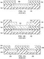
- FIG. 1B A typical example of forming an aluminum bond pad 110 on a top layer of copper interconnect 102 is illustrated in FIG. 1B .
- the underlying copper interconnect layer 102 is formed in a dielectric layer 100 using either a single or a dual damascene process.
- An opening is formed in dielectric layer 104 overlying the copper interconnect layer to form electrical connection to an overlying aluminum bondpad 110.
- An interdiffusion barrier layer 106 of a material such as Ta or TaN is disposed between the underlying copper interconnect and the overlying aluminum bondpad 110 to prevent interdiffusion of copper and aluminum.
- FIG. 2B A typical example of forming an upper level of aluminum interconnect 210 on a lower layer of copper interconnect 202 is illustrated in FIG. 2B .
- the underlying copper interconnect layer 202 is formed in a dielectric layer 200 using either a single or a dual damascene process.
- Contact or via openings are formed in dielectric layer 204 overlying the copper interconnect layer 202 to form electrical connection between the interconnect layers 202 and 210.
- An interdiffusion barrier layer 206 of a material such as Ta or TaN is disposed between the underlying copper interconnect 202 and the overlying aluminum interconnect 210 to prevent interdiffusion of copper and aluminum.
- the TaxOy (or TaxNyOz) layer that forms on the TaN interdiffusion barrier layer 106 ( FIG. 1A ) and layer 206 ( FIG. 2A ) causes the contact resistance to increase by 6x after 12 hours of exposure to air and by 10x after 24 hours of exposure to air.
- the increase in electrical contact resistance caused by the TaxOy layer typically varies significantly from contact to contact. The magnitude of the increase in electrical resistance depends on both the test structure and measurement technique used.
- TABLE 1 was generated from 4-point probe measurements to maximize sensitivity to interface resistance and is intended solely to provide a baseline reference for quantifying the improvement afforded by an example embodiment.
- TABLE 1 TaN in via exposure to air Resistance Increase 12 hours 6x 24 hours 10x
- the metal oxide layer may be removed by various means such as sputter etching before deposition of the aluminum bondpad metal 110 or the upper aluminum interconnect metal 210, but this often causes other problems.
- sputter etching before deposition of the aluminum bondpad metal 110 or the upper aluminum interconnect metal 210, but this often causes other problems.
- an argon sputter etch is used to remove the TaxOy layer that forms on the TaN barrier layer 106 and 206 before AlCu 110 and 210 deposition
- the sputter etch process introduces particles which reduces yield.
- the presputter etch alters the morphology of the deposited AlCu, 110 or 210, resulting in a decrease in electromigration resistance.
- GB 2 384 114 A discloses Ti-rich TiNx barriers for Al interconnects with an N-concentration as low as 41 at.%.
- US2004/0183202 A1 discloses a Cu interconnect with a Ta-rich TaNx barrier layer with 15-40 at.% N-content.
- an integrated circuit includes an underlying metal geometry, a dielectric layer on the underlying metal geometry, a contact opening through the dielectric layer, an overlying metal geometry wherein a portion of the overlying metal geometry fills a portion of the contact opening, and an oxidation resistant barrier layer disposed between the underlying metal geometry and overlying metal geometry.
- the oxidation resistant barrier layer is formed of TaN or TiN with a nitrogen content of at least 20 atomic % and a thickness of at least 5 nm. The oxidation resistant barrier layer extends under the contact opening.
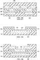
- FIG. 3B An aluminum copper (AlCu) bondpad 110 to underlying copper interconnect 102 structure with an interdiffusion barrier layer 106 and with an oxidation resistant barrier layer 320 is illustrated in FIG. 3B .
- a copper interconnect geometry 102 is formed in a dielectric layer 100 using a damascene process.
- a dielectric layer 104 with a contact opening to the copper interconnect geometry 102 overlies dielectric layer 100 and copper interconnect geometry 102.
- a bondpad stack including an interdiffusion barrier layer 106, an oxidation resistant barrier surface (ORBS) layer 320 and aluminum or aluminum copper alloy 110 overlies the dielectric layer 104 and contacts the underlying copper interconnect geometry 102 through the contact opening in dielectric layer 104.
- ORBS oxidation resistant barrier surface
- the interdiffusion barrier layer 106 may be a material such as TaN or TiN with a thickness between about 60 nm and 90 nm, and a nitrogen content between about 0 and 12 atomic percent.
- the ORBS layer 320 may be nitrogen rich tantalum nitride with nitrogen content in the range of about 20 to 35 atomic percent and a thickness in the range of about 5 nm to 15 nm.
- the ORBS layer 320 may also be a nitrogen rich titanium nitride with a thickness slightly higher than the nitrogen rich tantalum nitride oxidation resistant layer.
- An aluminum copper (AlCu) interconnect 210 to underlying copper interconnect 202 structure with an interdiffusion barrier layer 206 and with an oxidation resistant barrier layer 420 is illustrated in FIG. 4B .
- a copper interconnect geometry 202 is formed in a dielectric layer 200 using a damascene process.
- a dielectric layer 204 with contact or via openings to the copper interconnect geometries 202 overlies dielectric layer 200 and copper interconnect geometries 202.
- a upper aluminum interconnect stack including an interdiffusion barrier layer 206, an oxidation resistant barrier surface (ORBS) layer 420 and aluminum or aluminum copper alloy 210 overlies the dielectric layer 204 and contacts the underlying copper interconnect geometries 202 through the contact or via openings in dielectric layer 204.
- ORBS oxidation resistant barrier surface
- the interdiffusion barrier layer 206 may be a material such as TaN or TiN with a thickness between about 60 nm and 90 nm, and a nitrogen content between about 0 and 12 atomic percent.
- the ORBS layer 420 may be nitrogen rich tantalum nitride with nitrogen content in the range of about 20 to 35 atomic percent and a thickness in the range of about 5 nm to 15 nm.
- the ORBS layer 420 may also be a nitrogen rich titanium nitride with a thickness slightly higher than the nitrogen rich tantalum nitride oxidation resistant layer.
- the ORBS layers 320 and 420 enable the IC to be exposed to air for 24 hours or longer before deposition of the bondpad metal 110 or the upper aluminum interconnect metal 210 with an increase in contact resistance of less than 2x. Also, with the ORBS layers 320 and 420, the resistance of many contacts or vias across the integrated circuit (IC) chip and across the IC wafer remains tightly distributed.
- a copper interconnect interdiffusion barrier layer with an oxidation resistant barrier layer structure is used for illustration.
- an interdiffusion barrier layer 106 or 206 is required to prevent interdiffusion of copper and aluminum.
- the underlying interconnect layer is another material such as TiW or W which does not interdiffuse with AlCu, the barrier layer 106 or 206 may be omitted and the ORBS layer 320 or 420 may be deposited directly on the underlying interconnect.
- Overlying aluminum or aluminum copper is used in FIGS. 3 and 4 for illustration.
- Other overlying metals such as nickel palladium alloy may be used for the overlying bondpad 110 or overlying interconnect 210 material instead of aluminum or aluminum copper.
- a contact opening may be formed in a dielectric layer that overlies the underlying metal layer and the ORBS layer may be deposited on the dielectric layer and into the contact opening as described above.
- the ORBS layer is deposited on the underlying metal layer (or on a barrier layer on the underlying metal layer) before patterning and etching to form the underlying metal layer geometry.
- a contact opening is etched through an overlying dielectric layer stopping on the ORBS layer. This contact opening with the ORBS layer in the bottom may be exposed to air for an extended time (up to 24 hours) with little (less than 2x) increase in contact resistance.
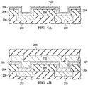
- FIG. 5B A structure in which the underlying metal layer 510 is deposited, patterned and etched and the oxidation resistant barrier layer 520 is deposited into a contact opening in a dielectric 104 overlying the underlying metal layer 510 is illustrated in FIG. 5B .
- the underlying metal layer 510 to which contact is made may be a metal resistor or an electrical fuse (efuse) or a top plate of a metal-to-metal capacitor for example.
- the oxidation resistant barrier layer 520 is deposited into openings in the dielectric 104 overlying the metal layer 510 to form electrical contact to underlying metal layer 510, as shown in FIG. 5A .
- Top metal 110 which overlies the oxidation resistant barrier 520 may be used to form a bondpad or may be used as an upper layer of interconnect. In this example, a metal which does not require an interdiffusion barrier layer is used for illustration so the oxidation resistant barrier 520 may be deposited directly onto the underlying metal layer 510.
- the ORBS layer (which may be nitrogen rich TaN as described hereinabove) provides low and consistent contact resistance across a wafer and also increases the span of time (process window) that the wafer may be exposed to air between oxidation resistant barrier layer 520 deposition and top metal 110 deposition thus improving manufacturability.
- FIG. 6B A structure in which an embodiment oxidation resistant barrier layer 620 is deposited on the underlying metal layer 610 before patterning and etching to form the underlying metal layer 610 geometry is shown in FIG. 6B .
- the lower metal layer 610 may be a top capacitor plate or a metal resistor.
- An optional interdiffusion barrier layer may be deposited on the underlying metal layer 610 before deposition of the ORBS layer 620 if needed.
- contact or via openings are etched through an overlying dielectric layer 104 and stop on the ORBS layer 620 which is on top of the underlying metal layer 610, as shown in FIG. 6A .
- the top metal 110 is deposited directly onto the ORBS layer 620 that is exposed in the bottom of the contact or via openings.
- the ORBS layer 620 may be exposed to air for up to 24 hours with less than a 2x increase in resistance. Also, the distribution of contact or via resistance across contacts across an IC chip or across an IC wafer remains tightly distributed.
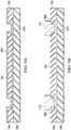
- FIG. 7 is a process flow diagram for a method for forming contacts using an ORBS layer such as those shown in FIGS. 3A, 3B , 4A, 4B , and 5A and 5B .
- a contact pattern is formed on a dielectric layer 104 overlying the underlying metal 102 ( FIG. 3A ) or 202 ( FIG. 4A ) or 510 ( FIG. 5A ) and openings are etched through the dielectric layer 104 ( FIGS. 3A , 5A ) or 204 ( FIG. 4A ) stopping on the underlying metal layer 102/202/510.
- an optional interdiffusion barrier layer 106 ( FIG. 3A ) or 206 ( FIG. 4B ) may be deposited over the dielectric layer 104 or 204 and into the contact opening.
- a degas step (such as a bake at a temperature in the range of 250°C to 400 °C under reduced pressure) and/or a presputter clean step (such as an argon presputter clean) or a reactive preclean (such as a high bias preclean with hydrogen plus argon or hydrogen plus helium) may be performed before the interdiffusion barrier layer 106 ( FIG. 3A ) or 206 ( FIG. 4A ) deposition.
- FIG. 3A and 4A illustrate a process flow that incorporates the optional interdiffusion barrier layer 106 or 206.
- FIG. 5A illustrates a process flow that does not incorporate an interdiffusion barrier layer.
- the interdiffusion barrier layer may be TaN or TiN with a thickness between about 60 nm and 90 nm and a nitrogen content between about 0 atomic % and 12 atomic %.
- the oxidation resistance barrier surface (ORBS) layer, 320 ( FIG. 3A ) or 420 ( FIG. 4A ) is deposited.
- the ORBS layer, 320 ( FIG. 3A ) or 420 ( FIG. 4A ) may be a high nitrogen content TaN layer with a thickness between about 5 nm and 15 nm and a nitrogen content of about 20 atomic % to 35 atomic %.
- One tool that the ORBS film may be deposited in is an EnCoRe1 chamber on the Applied Endura platform.
- the ORBS layer may be deposited at room temperature with a pressure between about 2.5 and 5 torr, a power in the range of 15 to 30 KW, a bias in the range of 250 W to 500 W and a flow rate of nitrogen in the range of about 115 to 125 sccm.
- the deposition time may vary depending upon the deposition conditions. A time sufficient to deposit a TaN film with a thickness in the range of 5 nm to 15 nm is used.
- ORBS TaN film with a thickness in the range of 5 nm to 15 nm and a nitrogen content in the range of 20 atomic % to 35 atomic %.
- the ORBS film may be exposed to air for an extended length of time if desired. At least a short exposure to air may be desirable. The air exposure may affect the grain structure and electromigration resistance of subsequently deposited interconnect or bondpad metal.
- the ORBS film enables the IC wafer to be exposed to air for an extended period of time (24 hours) with less than a 2x increase in resistance. Also, the distribution of resistance of all the contacts across an IC chip and across an IC wafer remains tightly distributed.
- step 708 an upper metal used for either interconnect or bondpad formation is deposited on the oxidation resistant barrier surface (ORBS) layer.
- ORBS oxidation resistant barrier surface
- step 710 the upper metal used for either interconnect or bondpad formation is patterned.
- step 712 the upper metal used for either interconnect or bondpad formation is etched and the ORBS material is etched.
- step 714 the interdiffusion barrier layer is etched if it exists.
- FIG. 8 is a process flow diagram for a method for forming contacts using an ORBS layer 620 ( FIG. 6A ) that is deposited on an underlying metal layer 610 before patterning and etching to form the underlying metal geometry 610 is shown in FIGS. 6A and 6B .
- step 800 the underlying metal layer 610 is deposited.
- an optional interdiffusion barrier layer is deposited to prevent interdiffusion of the underlying metal layer 610 with the overlying metal layer 110 if it is needed. If it is not needed, the embodiment ORBS layer 620 may be deposited directly on the underlying metal layer 610. If the underlying metal layer has been exposed to air, a degas step may be used. The degas step (such as a bake at 250 C to 400 C under reduced pressure) and/or a presputter clean step (such as an argon presputter clean) or a reactive preclean (such as a high bias preclean with hydrogen plus argon or hydrogen plus helium) may be performed before the ORBS layer 620 deposition.
- a presputter clean step such as an argon presputter clean
- a reactive preclean such as a high bias preclean with hydrogen plus argon or hydrogen plus helium
- the ORBS layer 620 is deposited on the underlying metal layer 610.
- the ORBS layer 620 may be a high nitrogen content TaN layer with a thickness between about 5 nm and 15 nm and a nitrogen content of about 20 atomic % to 35 atomic %.
- One tool that the ORBS film may be deposited in is an EnCoRe1 chamber on the Applied Endura platform. In this tool The ORBS layer may be deposited at room temperature with a pressure between about 2.5 to 5 torr, a power in the range of 15 to 30 KW, a bias in the range of 250 W to 500 W and a flow rate of nitrogen in the range of about 115 to 125 sccm.
- the deposition time may vary depending upon the deposition conditions. A time sufficient to deposit a TaN film with a thickness in the range of 5 nm to 15 nm is used.
- ORBS TaN film with a thickness in the range of 5 nm to 15 nm and a nitrogen content in the range of 20 atomic % to 35 atomic %.
- step 806 the underlying metal is patterned and etched to form the underlying interconnect geometry 610.
- the ORBS layer 620 is etched first.
- the optional interdiffusion barrier layer is etched next if it exists.
- the underlying metal 610 is then etched.
- a dielectric layer 104 such as silicon dioxide or polyimide is deposited over the underlying dielectric 100 and metal layer 610.
- a pattern is formed on the dielectric layer 104 with openings over the underlying metal geometry 610.
- the dielectric material is etched out of the openings stopping on the ORBS layer 620.
- the ORBS layer 620 enables the IC wafers to be exposed to air for an extended period of time (24 hours) with little (less than 2x) increase in resistance. Also, the ORBS layer 620 provides for a tight distribution of contact resistance across the IC chip and across the IC wafer.
- step 812 an upper metal used for either interconnect or bondpad formation is deposited on the dielectric layer 104 and on the oxidation resistant (ORBS) barrier layer in the bottom of the contact openings.
- ORBS oxidation resistant
- step 814 the upper metal used for either interconnect or bondpad formation is patterned and etched to form the upper interconnect metal geometries 110.
Description
- This relates generally to integrated circuits, and more particularly to formation of contacts with stable resistance in integrated circuits.
- During processing of an integrated circuit, openings typically referred to as contacts or vias are made through dielectric overlying metal interconnect leads to form electrical contact to the leads. The metal interconnect that is exposed in these contact or via openings may form a layer of metal oxide on the surface that increases the electrical contact resistance and also may cause significant variation in the electrical contact resistance in these openings across an integrated circuit chip or wafer.
- A typical example of forming an
aluminum bond pad 110 on a top layer ofcopper interconnect 102 is illustrated inFIG. 1B . The underlyingcopper interconnect layer 102 is formed in adielectric layer 100 using either a single or a dual damascene process. An opening is formed indielectric layer 104 overlying the copper interconnect layer to form electrical connection to anoverlying aluminum bondpad 110. Aninterdiffusion barrier layer 106 of a material such as Ta or TaN is disposed between the underlying copper interconnect and the overlyingaluminum bondpad 110 to prevent interdiffusion of copper and aluminum. - A typical example of forming an upper level of
aluminum interconnect 210 on a lower layer ofcopper interconnect 202 is illustrated inFIG. 2B . The underlyingcopper interconnect layer 202 is formed in adielectric layer 200 using either a single or a dual damascene process. Contact or via openings are formed indielectric layer 204 overlying thecopper interconnect layer 202 to form electrical connection between theinterconnect layers interdiffusion barrier layer 206 of a material such as Ta or TaN is disposed between theunderlying copper interconnect 202 and the overlyingaluminum interconnect 210 to prevent interdiffusion of copper and aluminum. - As illustrated in TABLE 1, the TaxOy (or TaxNyOz) layer that forms on the TaN interdiffusion barrier layer 106 (
FIG. 1A ) and layer 206 (FIG. 2A ) causes the contact resistance to increase by 6x after 12 hours of exposure to air and by 10x after 24 hours of exposure to air. Also, the increase in electrical contact resistance caused by the TaxOy layer typically varies significantly from contact to contact. The magnitude of the increase in electrical resistance depends on both the test structure and measurement technique used. TABLE 1 was generated from 4-point probe measurements to maximize sensitivity to interface resistance and is intended solely to provide a baseline reference for quantifying the improvement afforded by an example embodiment.TABLE 1 TaN in via exposure to air Resistance Increase 12 hours 6x 24 hours 10x - The metal oxide layer may be removed by various means such as sputter etching before deposition of the
aluminum bondpad metal 110 or the upper aluminum interconnectmetal 210, but this often causes other problems. For example if an argon sputter etch is used to remove the TaxOy layer that forms on theTaN barrier layer AlCu -
GB 2 384 114 A -
US2004/0183202 A1 discloses a Cu interconnect with a Ta-rich TaNx barrier layer with 15-40 at.% N-content. - The invention is defined in claims 1 and 6.
- In described examples, an integrated circuit includes an underlying metal geometry, a dielectric layer on the underlying metal geometry, a contact opening through the dielectric layer, an overlying metal geometry wherein a portion of the overlying metal geometry fills a portion of the contact opening, and an oxidation resistant barrier layer disposed between the underlying metal geometry and overlying metal geometry. The oxidation resistant barrier layer is formed of TaN or TiN with a nitrogen content of at least 20 atomic % and a thickness of at least 5 nm. The oxidation resistant barrier layer extends under the contact opening.
-
-
FIGS. 1A and 1B (prior art) are cross-sections of a lower copper interconnect to upper aluminum bondpad metal contact with an interdiffusion barrier in the bottom of the contact. -
FIGS. 2A and2B (prior art) are cross-sections of a lower copper interconnect to upper aluminum interconnect metal contact with an interdiffusion barrier in the bottom of the contact. -
FIGS. 3A and 3B are cross-sections of a lower copper interconnect to upper aluminum bondpad contact with an interdiffusion barrier plus an oxidation resistant barrier. -
FIGS. 4A and 4B are cross-sections of a lower copper interconnect to upper aluminum interconnect contact with an interdiffusion barrier plus an oxidation resistant barrier layer. -
FIGS. 5A and 5B are cross-sections of a lower metal to upper metal contact with an oxidation resistant barrier layer formed wherein the oxidation resistant barrier layer covers the sidewalls and the bottom of the contact. -
FIGS. 6A and 6B are cross-sections of a lower metal to upper metal contact with an oxidation resistant barrier layer formed according to principles of example embodiments, wherein the oxidation resistant barrier layer covers the lower metal geometry. -
FIG. 7 is a flow diagram describing the primary manufacturing steps to form the contact structures depicted inFIGS. 2A ,2B, 3A, 3B ,4A, 4B ,5A and 5B . -
FIG. 8 is a flow diagram describing the primary manufacturing steps to form the contact structures depicted inFIGS. 6A and 6B . - The figures are not necessarily drawn to scale. Some illustrated ordering of acts or events may occur in different orders and/or concurrently with other acts or events. Furthermore, not all illustrated acts or events are required to implement a methodology in accordance with example embodiments.
- An aluminum copper (AlCu)
bondpad 110 to underlyingcopper interconnect 102 structure with aninterdiffusion barrier layer 106 and with an oxidationresistant barrier layer 320 is illustrated inFIG. 3B . Acopper interconnect geometry 102 is formed in adielectric layer 100 using a damascene process. Adielectric layer 104 with a contact opening to thecopper interconnect geometry 102 overliesdielectric layer 100 andcopper interconnect geometry 102. A bondpad stack including aninterdiffusion barrier layer 106, an oxidation resistant barrier surface (ORBS)layer 320 and aluminum oraluminum copper alloy 110 overlies thedielectric layer 104 and contacts the underlyingcopper interconnect geometry 102 through the contact opening indielectric layer 104. Theinterdiffusion barrier layer 106 may be a material such as TaN or TiN with a thickness between about 60 nm and 90 nm, and a nitrogen content between about 0 and 12 atomic percent. The ORBSlayer 320 may be nitrogen rich tantalum nitride with nitrogen content in the range of about 20 to 35 atomic percent and a thickness in the range of about 5 nm to 15 nm. The ORBSlayer 320 may also be a nitrogen rich titanium nitride with a thickness slightly higher than the nitrogen rich tantalum nitride oxidation resistant layer. - An aluminum copper (AlCu) interconnect 210 to underlying
copper interconnect 202 structure with aninterdiffusion barrier layer 206 and with an oxidationresistant barrier layer 420 is illustrated inFIG. 4B . Acopper interconnect geometry 202 is formed in adielectric layer 200 using a damascene process. Adielectric layer 204 with contact or via openings to thecopper interconnect geometries 202 overliesdielectric layer 200 andcopper interconnect geometries 202. A upper aluminum interconnect stack including aninterdiffusion barrier layer 206, an oxidation resistant barrier surface (ORBS)layer 420 and aluminum oraluminum copper alloy 210 overlies thedielectric layer 204 and contacts the underlyingcopper interconnect geometries 202 through the contact or via openings indielectric layer 204. Theinterdiffusion barrier layer 206 may be a material such as TaN or TiN with a thickness between about 60 nm and 90 nm, and a nitrogen content between about 0 and 12 atomic percent. TheORBS layer 420 may be nitrogen rich tantalum nitride with nitrogen content in the range of about 20 to 35 atomic percent and a thickness in the range of about 5 nm to 15 nm. TheORBS layer 420 may also be a nitrogen rich titanium nitride with a thickness slightly higher than the nitrogen rich tantalum nitride oxidation resistant layer. - The ORBS layers 320 and 420 enable the IC to be exposed to air for 24 hours or longer before deposition of the
bondpad metal 110 or the upperaluminum interconnect metal 210 with an increase in contact resistance of less than 2x. Also, with the ORBS layers 320 and 420, the resistance of many contacts or vias across the integrated circuit (IC) chip and across the IC wafer remains tightly distributed. - A copper interconnect interdiffusion barrier layer with an oxidation resistant barrier layer structure is used for illustration. In this structure, an
interdiffusion barrier layer barrier layer ORBS layer - Overlying aluminum or aluminum copper is used in
FIGS. 3 and4 for illustration. Other overlying metals such as nickel palladium alloy may be used for theoverlying bondpad 110 oroverlying interconnect 210 material instead of aluminum or aluminum copper. - When the underlying metal layer is formed by deposition, pattern, and etch instead of by a damascene process, two options for the ORBS layer are available. As with an underlying metal geometry formed using a damascene process, a contact opening may be formed in a dielectric layer that overlies the underlying metal layer and the ORBS layer may be deposited on the dielectric layer and into the contact opening as described above. According to the invention, for metal geometries formed by deposition, pattern, and etch the ORBS layer is deposited on the underlying metal layer (or on a barrier layer on the underlying metal layer) before patterning and etching to form the underlying metal layer geometry. In this alternative structure a contact opening is etched through an overlying dielectric layer stopping on the ORBS layer. This contact opening with the ORBS layer in the bottom may be exposed to air for an extended time (up to 24 hours) with little (less than 2x) increase in contact resistance.
- A structure in which the
underlying metal layer 510 is deposited, patterned and etched and the oxidationresistant barrier layer 520 is deposited into a contact opening in a dielectric 104 overlying theunderlying metal layer 510 is illustrated inFIG. 5B . Theunderlying metal layer 510 to which contact is made may be a metal resistor or an electrical fuse (efuse) or a top plate of a metal-to-metal capacitor for example. - The oxidation
resistant barrier layer 520 is deposited into openings in the dielectric 104 overlying themetal layer 510 to form electrical contact tounderlying metal layer 510, as shown inFIG. 5A .Top metal 110 which overlies the oxidationresistant barrier 520 may be used to form a bondpad or may be used as an upper layer of interconnect. In this example, a metal which does not require an interdiffusion barrier layer is used for illustration so the oxidationresistant barrier 520 may be deposited directly onto theunderlying metal layer 510. - The ORBS layer (which may be nitrogen rich TaN as described hereinabove) provides low and consistent contact resistance across a wafer and also increases the span of time (process window) that the wafer may be exposed to air between oxidation
resistant barrier layer 520 deposition andtop metal 110 deposition thus improving manufacturability. - A structure in which an embodiment oxidation
resistant barrier layer 620 is deposited on theunderlying metal layer 610 before patterning and etching to form theunderlying metal layer 610 geometry is shown inFIG. 6B . For example, thelower metal layer 610 may be a top capacitor plate or a metal resistor. An optional interdiffusion barrier layer may be deposited on theunderlying metal layer 610 before deposition of theORBS layer 620 if needed. - In this structure, contact or via openings are etched through an overlying
dielectric layer 104 and stop on theORBS layer 620 which is on top of theunderlying metal layer 610, as shown inFIG. 6A . Thetop metal 110 is deposited directly onto theORBS layer 620 that is exposed in the bottom of the contact or via openings. TheORBS layer 620 may be exposed to air for up to 24 hours with less than a 2x increase in resistance. Also, the distribution of contact or via resistance across contacts across an IC chip or across an IC wafer remains tightly distributed. -
FIG. 7 is a process flow diagram for a method for forming contacts using an ORBS layer such as those shown inFIGS. 3A, 3B ,4A, 4B , and5A and 5B . - In
step 700, a contact pattern is formed on adielectric layer 104 overlying the underlying metal 102 (FIG. 3A ) or 202 (FIG. 4A ) or 510 (FIG. 5A ) and openings are etched through the dielectric layer 104 (FIGS. 3A ,5A ) or 204 (FIG. 4A ) stopping on theunderlying metal layer 102/202/510. - In
step 702, an optional interdiffusion barrier layer 106 (FIG. 3A ) or 206 (FIG. 4B ) may be deposited over thedielectric layer FIG. 3A ) or 206 (FIG. 4A ) deposition.FIGS. 3A and4A illustrate a process flow that incorporates the optionalinterdiffusion barrier layer FIG. 5A illustrates a process flow that does not incorporate an interdiffusion barrier layer. The interdiffusion barrier layer may be TaN or TiN with a thickness between about 60 nm and 90 nm and a nitrogen content between about 0 atomic % and 12 atomic %. - In
step 704, the oxidation resistance barrier surface (ORBS) layer, 320 (FIG. 3A ) or 420 (FIG. 4A ) is deposited. The ORBS layer, 320 (FIG. 3A ) or 420 (FIG. 4A ), may be a high nitrogen content TaN layer with a thickness between about 5 nm and 15 nm and a nitrogen content of about 20 atomic % to 35 atomic %. One tool that the ORBS film may be deposited in is an EnCoRe1 chamber on the Applied Endura platform. In this tool, the ORBS layer may be deposited at room temperature with a pressure between about 2.5 and 5 torr, a power in the range of 15 to 30 KW, a bias in the range of 250 W to 500 W and a flow rate of nitrogen in the range of about 115 to 125 sccm. The deposition time may vary depending upon the deposition conditions. A time sufficient to deposit a TaN film with a thickness in the range of 5 nm to 15 nm is used. - Other deposition tools with different deposition conditions may be used to produce an equivalent ORBS TaN film with a thickness in the range of 5 nm to 15 nm and a nitrogen content in the range of 20 atomic % to 35 atomic %.
- In
step 706, the ORBS film may be exposed to air for an extended length of time if desired. At least a short exposure to air may be desirable. The air exposure may affect the grain structure and electromigration resistance of subsequently deposited interconnect or bondpad metal. The ORBS film enables the IC wafer to be exposed to air for an extended period of time (24 hours) with less than a 2x increase in resistance. Also, the distribution of resistance of all the contacts across an IC chip and across an IC wafer remains tightly distributed. - In
step 708, an upper metal used for either interconnect or bondpad formation is deposited on the oxidation resistant barrier surface (ORBS) layer. - In
step 710, the upper metal used for either interconnect or bondpad formation is patterned. - In
step 712, the upper metal used for either interconnect or bondpad formation is etched and the ORBS material is etched. - In
step 714, the interdiffusion barrier layer is etched if it exists. -
FIG. 8 is a process flow diagram for a method for forming contacts using an ORBS layer 620 (FIG. 6A ) that is deposited on anunderlying metal layer 610 before patterning and etching to form theunderlying metal geometry 610 is shown inFIGS. 6A and 6B . - In
step 800, theunderlying metal layer 610 is deposited. - In
step 802, an optional interdiffusion barrier layer is deposited to prevent interdiffusion of theunderlying metal layer 610 with the overlyingmetal layer 110 if it is needed. If it is not needed, theembodiment ORBS layer 620 may be deposited directly on theunderlying metal layer 610. If the underlying metal layer has been exposed to air, a degas step may be used. The degas step (such as a bake at 250 C to 400 C under reduced pressure) and/or a presputter clean step (such as an argon presputter clean) or a reactive preclean (such as a high bias preclean with hydrogen plus argon or hydrogen plus helium) may be performed before theORBS layer 620 deposition. - In
step 804, theORBS layer 620 is deposited on theunderlying metal layer 610. TheORBS layer 620 may be a high nitrogen content TaN layer with a thickness between about 5 nm and 15 nm and a nitrogen content of about 20 atomic % to 35 atomic %. One tool that the ORBS film may be deposited in is an EnCoRe1 chamber on the Applied Endura platform. In this tool The ORBS layer may be deposited at room temperature with a pressure between about 2.5 to 5 torr, a power in the range of 15 to 30 KW, a bias in the range of 250 W to 500 W and a flow rate of nitrogen in the range of about 115 to 125 sccm. The deposition time may vary depending upon the deposition conditions. A time sufficient to deposit a TaN film with a thickness in the range of 5 nm to 15 nm is used. - Other deposition tools with different deposition conditions may be used to produce an equivalent ORBS TaN film with a thickness in the range of 5 nm to 15 nm and a nitrogen content in the range of 20 atomic % to 35 atomic %.
- In
step 806, the underlying metal is patterned and etched to form theunderlying interconnect geometry 610. TheORBS layer 620 is etched first. The optional interdiffusion barrier layer is etched next if it exists. Theunderlying metal 610 is then etched. - In
step 808, adielectric layer 104 such as silicon dioxide or polyimide is deposited over theunderlying dielectric 100 andmetal layer 610. - In
step 810, a pattern is formed on thedielectric layer 104 with openings over theunderlying metal geometry 610. The dielectric material is etched out of the openings stopping on theORBS layer 620. TheORBS layer 620 enables the IC wafers to be exposed to air for an extended period of time (24 hours) with little (less than 2x) increase in resistance. Also, theORBS layer 620 provides for a tight distribution of contact resistance across the IC chip and across the IC wafer. - In
step 812, an upper metal used for either interconnect or bondpad formation is deposited on thedielectric layer 104 and on the oxidation resistant (ORBS) barrier layer in the bottom of the contact openings. - In
step 814, the upper metal used for either interconnect or bondpad formation is patterned and etched to form the upperinterconnect metal geometries 110. - Modifications are possible in the described embodiments, and other embodiments are possible, within the scope of the claims.
Claims (11)
- An integrated circuit, comprising:an underlying metal geometry;a dielectric layer on the underlying metal geometry;a contact opening through the dielectric layer wherein the contact opening stops on the underlying metal geometry;an overlying metal geometry wherein a portion of the overlying metal geometry fills a portion of the contact opening; andan oxidation resistant barrier layer wherein the oxidation resistant barrier layer is disposed between the underlying metal geometry and overlying metal geometry and wherein the oxidation resistant barrier layer is formed of TaN or TiN with a nitrogen content of at least 20 atomic percent and a thickness of at least 5 nm, characterized in that the oxidation resistant barrier layer extends under the contact opening.
- The integrated circuit of claim 1 further comprising an interdiffusion barrier layer disposed between the underlying metal geometry and the oxidation resistant barrier layer.
- The integrated circuit of claim wherein the interdiffusion barrier layer is TaN or TiN with a thickness between 60 nm and 90 nm and a nitrogen content between 0 and 12 atomic percent.
- The integrated circuit of claim 1 wherein the oxidation resistant barrier layer is formed of TaN with a thickness between 5 and 15 nm and with a nitrogen content between 20 and 35 atomic percent.
- The integrated circuit of any preceding claim wherein the oxidation resistant barrier layer is formed of TaN with a thickness of about 10 nm and a nitrogen content of about 28 atomic percent.
- A process of forming an integrated circuit, the process comprising:forming an underlying metal geometry on a first dielectric;depositing a second dielectric layer over the underlying metal geometry and over the first dielectric;forming a contact photo resist pattern on the second dielectric layer with a contact opening over the underlying metal geometry;etching a contact opening through the second dielectric layer and stopping on the underlying metal geometry;depositing an overlying metal layer in the contact opening;forming an oxidation resistant barrier layer between the underlying metal geometry and the overlying metal layer wherein the oxidation resistant barrier layer is TaN or TiN with a nitrogen content of at least 20 atomic percent and a thickness of at least 5 nm;forming a photo resist pattern on the overlying metal layer with an overlying metal geometry covering the contact opening; andetching the overlying metal layer to form the overlying metal geometry, characterized in that the oxidation resistant barrier layer is deposited on the underlying metal geometry before depositing the second dielectric layer.
- The process of claim 6, further comprising: exposing the oxidation resistant barrier layer to air for a period of time up to 24 hours before the step of depositing the overlying metal layer.
- The process of claim 6, further comprising: depositing an interdiffusion barrier layer before the step of depositing the oxidation resistant barrier layer.
- The process of claim 8, wherein the interdiffusion barrier layer is a TaN or TiN layer with a thickness between 60 nm and 90 nm and a nitrogen content in the range of 0 to 12 atomic percent.
- The process of claim 6, wherein the oxidation resistance barrier layer is a TaN layer with a thickness in the range of 5 nm to 15 nm and a nitrogen content in the range of 20 to 35 atomic percent.
- The process of claim 6, wherein the oxidation resistant barrier layer is TaN with a thickness in the range of 5 nm to 15 nm deposited at room temperature with a pressure between about 2.5 to 5 torr, a power in the range of 15 to 30 KW, a bias in the range of 250 W to 500 W, and a flow rate of nitrogen in the range of about 115 to 125 sccm.
Applications Claiming Priority (2)
| Application Number | Priority Date | Filing Date | Title |
|---|---|---|---|
| US14/974,012 US9704804B1 (en) | 2015-12-18 | 2015-12-18 | Oxidation resistant barrier metal process for semiconductor devices |
| PCT/US2016/067495 WO2017106828A1 (en) | 2015-12-18 | 2016-12-19 | Oxidation resistant barrier metal process for semiconductor devices |
Publications (3)
| Publication Number | Publication Date |
|---|---|
| EP3391408A1 EP3391408A1 (en) | 2018-10-24 |
| EP3391408A4 EP3391408A4 (en) | 2018-12-19 |
| EP3391408B1 true EP3391408B1 (en) | 2020-06-03 |
Family
ID=59057739
Family Applications (1)
| Application Number | Title | Priority Date | Filing Date |
|---|---|---|---|
| EP16876903.2A Active EP3391408B1 (en) | 2015-12-18 | 2016-12-19 | Oxidation resistant barrier metal for semiconductor devices and corresponding process |
Country Status (5)
| Country | Link |
|---|---|
| US (3) | US9704804B1 (en) |
| EP (1) | EP3391408B1 (en) |
| JP (1) | JP7111935B2 (en) |
| CN (1) | CN108352328A (en) |
| WO (1) | WO2017106828A1 (en) |
Families Citing this family (8)
| Publication number | Priority date | Publication date | Assignee | Title |
|---|---|---|---|---|
| US9954166B1 (en) * | 2016-11-28 | 2018-04-24 | Taiwan Semiconductor Manufacturing Co., Ltd. | Embedded memory device with a composite top electrode |
| US10304772B2 (en) | 2017-05-19 | 2019-05-28 | Taiwan Semiconductor Manufacturing Co., Ltd. | Semiconductor device structure with resistive element |
| JP6872991B2 (en) * | 2017-06-29 | 2021-05-19 | ルネサスエレクトロニクス株式会社 | Semiconductor devices and their manufacturing methods |
| US10985011B2 (en) | 2017-11-09 | 2021-04-20 | Taiwan Semiconductor Manufacturing Co., Ltd. | Structure and formation method of semiconductor device with resistive elements |
| US11309265B2 (en) * | 2018-07-30 | 2022-04-19 | Taiwan Semiconductor Manufacturing Co., Ltd. | Methods of fabricating semiconductor devices having conductive pad structures with multi-barrier films |
| KR102530319B1 (en) * | 2018-12-07 | 2023-05-09 | 삼성전자주식회사 | Semiconductor devices having a conductive pillar and methods of manufacturing the same |
| CN110676213B (en) * | 2019-09-18 | 2021-12-14 | 天津大学 | Silicon through hole interconnection copper wire barrier layer optimization method aiming at small line width requirement |
| US20220270979A1 (en) * | 2021-02-24 | 2022-08-25 | Applied Materials, Inc. | Formation of metal vias on metal lines |
Family Cites Families (41)
| Publication number | Priority date | Publication date | Assignee | Title |
|---|---|---|---|---|
| US4000055A (en) * | 1972-01-14 | 1976-12-28 | Western Electric Company, Inc. | Method of depositing nitrogen-doped beta tantalum |
| US5221449A (en) * | 1990-10-26 | 1993-06-22 | International Business Machines Corporation | Method of making Alpha-Ta thin films |
| US5358901A (en) * | 1993-03-01 | 1994-10-25 | Motorola, Inc. | Process for forming an intermetallic layer |
| MY115336A (en) * | 1994-02-18 | 2003-05-31 | Ericsson Telefon Ab L M | Electromigration resistant metallization structures and process for microcircuit interconnections with rf-reactively sputtered titanium tungsten and gold |
| US5962923A (en) * | 1995-08-07 | 1999-10-05 | Applied Materials, Inc. | Semiconductor device having a low thermal budget metal filling and planarization of contacts, vias and trenches |
| US6268291B1 (en) * | 1995-12-29 | 2001-07-31 | International Business Machines Corporation | Method for forming electromigration-resistant structures by doping |
| TW460597B (en) * | 1997-03-27 | 2001-10-21 | Applied Materials Inc | A barrier layer structure for use in semiconductors and a method of producing an aluminum-comprising layer having a 111 crystal orientation |
| US5925225A (en) * | 1997-03-27 | 1999-07-20 | Applied Materials, Inc. | Method of producing smooth titanium nitride films having low resistivity |
| US6153519A (en) * | 1997-03-31 | 2000-11-28 | Motorola, Inc. | Method of forming a barrier layer |
| US5893752A (en) * | 1997-12-22 | 1999-04-13 | Motorola, Inc. | Process for forming a semiconductor device |
| JP3456391B2 (en) * | 1997-07-03 | 2003-10-14 | セイコーエプソン株式会社 | Method for manufacturing semiconductor device |
| US5989623A (en) * | 1997-08-19 | 1999-11-23 | Applied Materials, Inc. | Dual damascene metallization |
| US7253109B2 (en) * | 1997-11-26 | 2007-08-07 | Applied Materials, Inc. | Method of depositing a tantalum nitride/tantalum diffusion barrier layer system |
| US20010055868A1 (en) * | 1998-05-22 | 2001-12-27 | Madan Sudhir K. | Apparatus and method for metal layer streched conducting plugs |
| JP2000124310A (en) | 1998-10-16 | 2000-04-28 | Matsushita Electronics Industry Corp | Semiconductor device and manufacture thereof |
| US20020000665A1 (en) * | 1999-04-05 | 2002-01-03 | Alexander L. Barr | Semiconductor device conductive bump and interconnect barrier |
| US6500750B1 (en) * | 1999-04-05 | 2002-12-31 | Motorola, Inc. | Semiconductor device and method of formation |
| US6376370B1 (en) * | 2000-01-18 | 2002-04-23 | Micron Technology, Inc. | Process for providing seed layers for using aluminum, copper, gold and silver metallurgy process for providing seed layers for using aluminum, copper, gold and silver metallurgy |
| US6339029B1 (en) * | 2000-01-19 | 2002-01-15 | Taiwan Semiconductor Manufacturing Company | Method to form copper interconnects |
| JP2001257327A (en) * | 2000-03-10 | 2001-09-21 | Nec Corp | Semiconductor device and its manufacturing method |
| JP2001257226A (en) | 2000-03-10 | 2001-09-21 | Hitachi Ltd | Semiconductor integrated circuit device |
| US6498091B1 (en) * | 2000-11-01 | 2002-12-24 | Applied Materials, Inc. | Method of using a barrier sputter reactor to remove an underlying barrier layer |
| US6521523B2 (en) * | 2001-06-15 | 2003-02-18 | Silicon Integrated Systems Corp. | Method for forming selective protection layers on copper interconnects |
| JP2003124211A (en) * | 2001-09-28 | 2003-04-25 | Agere Systems Inc | Structure and method for reducing electromigration |
| TWI278962B (en) * | 2002-04-12 | 2007-04-11 | Hitachi Ltd | Semiconductor device |
| US20040183202A1 (en) * | 2003-01-31 | 2004-09-23 | Nec Electronics Corporation | Semiconductor device having copper damascene interconnection and fabricating method thereof |
| JP3715975B2 (en) | 2003-04-24 | 2005-11-16 | 株式会社半導体理工学研究センター | Manufacturing method of multilayer wiring structure |
| US7265038B2 (en) * | 2003-11-25 | 2007-09-04 | Taiwan Semiconductor Manufacturing Co., Ltd. | Method for forming a multi-layer seed layer for improved Cu ECP |
| KR100642750B1 (en) * | 2005-01-31 | 2006-11-10 | 삼성전자주식회사 | Semiconductor device and method for manufacturing the same |
| JP5014632B2 (en) * | 2006-01-13 | 2012-08-29 | ルネサスエレクトロニクス株式会社 | Semiconductor device and manufacturing method of semiconductor device |
| US7405153B2 (en) * | 2006-01-17 | 2008-07-29 | International Business Machines Corporation | Method for direct electroplating of copper onto a non-copper plateable layer |
| US7276796B1 (en) * | 2006-03-15 | 2007-10-02 | International Business Machines Corporation | Formation of oxidation-resistant seed layer for interconnect applications |
| TW200814156A (en) * | 2006-07-21 | 2008-03-16 | Toshiba Kk | Method for manufacturing semiconductor device and semiconductor device |
| US7592257B2 (en) * | 2007-05-14 | 2009-09-22 | Tokyo Electron Limited | Semiconductor contact structure containing an oxidation-resistant diffusion barrier and method of forming |
| US7727882B1 (en) * | 2007-12-17 | 2010-06-01 | Novellus Systems, Inc. | Compositionally graded titanium nitride film for diffusion barrier applications |
| US8659155B2 (en) * | 2009-11-05 | 2014-02-25 | Taiwan Semiconductor Manufacturing Company, Ltd. | Mechanisms for forming copper pillar bumps |
| US8492891B2 (en) * | 2010-04-22 | 2013-07-23 | Taiwan Semiconductor Manufacturing Company, Ltd. | Cu pillar bump with electrolytic metal sidewall protection |
| US8872341B2 (en) * | 2010-09-29 | 2014-10-28 | Infineon Technologies Ag | Semiconductor structure having metal oxide or nirtride passivation layer on fill layer and method for making same |
| US8749060B2 (en) * | 2012-09-21 | 2014-06-10 | Taiwan Semiconductor Manufacturing Company, Ltd. | Method of semiconductor integrated circuit fabrication |
| US9455182B2 (en) * | 2014-08-22 | 2016-09-27 | International Business Machines Corporation | Interconnect structure with capping layer and barrier layer |
| US9613856B1 (en) * | 2015-09-18 | 2017-04-04 | Taiwan Semiconductor Manufacturing Company, Ltd. | Method of forming metal interconnection |
-
2015
- 2015-12-18 US US14/974,012 patent/US9704804B1/en active Active
-
2016
- 2016-12-19 EP EP16876903.2A patent/EP3391408B1/en active Active
- 2016-12-19 CN CN201680065355.6A patent/CN108352328A/en active Pending
- 2016-12-19 WO PCT/US2016/067495 patent/WO2017106828A1/en active Application Filing
- 2016-12-19 JP JP2018532131A patent/JP7111935B2/en active Active
-
2017
- 2017-06-07 US US15/615,963 patent/US10008450B2/en active Active
-
2018
- 2018-06-18 US US16/010,642 patent/US10665543B2/en active Active
Non-Patent Citations (1)
| Title |
|---|
| None * |
Also Published As
| Publication number | Publication date |
|---|---|
| JP2018538700A (en) | 2018-12-27 |
| US20170179033A1 (en) | 2017-06-22 |
| US20180308802A1 (en) | 2018-10-25 |
| EP3391408A4 (en) | 2018-12-19 |
| EP3391408A1 (en) | 2018-10-24 |
| WO2017106828A1 (en) | 2017-06-22 |
| US9704804B1 (en) | 2017-07-11 |
| JP7111935B2 (en) | 2022-08-03 |
| US10008450B2 (en) | 2018-06-26 |
| US10665543B2 (en) | 2020-05-26 |
| US20170271269A1 (en) | 2017-09-21 |
| CN108352328A (en) | 2018-07-31 |
Similar Documents
| Publication | Publication Date | Title |
|---|---|---|
| EP3391408B1 (en) | Oxidation resistant barrier metal for semiconductor devices and corresponding process | |
| US6373137B1 (en) | Copper interconnect for an integrated circuit and methods for its fabrication | |
| JP4555540B2 (en) | Semiconductor device | |
| US20100230815A1 (en) | Semiconductor device | |
| US20070123009A1 (en) | Technique for increasing adhesion of metallization layers by providing dummy vias | |
| KR101258369B1 (en) | In-situ formation of silicon and tantalum containing barrier | |
| US20120034760A1 (en) | Metallization for Chip Scale Packages in Wafer Level Packaging | |
| US8637402B2 (en) | Conductive line structure and the method of forming the same | |
| US7939421B2 (en) | Method for fabricating integrated circuit structures | |
| US20100190335A1 (en) | Method of manufacturing semiconductor device | |
| US7323409B2 (en) | Method for forming a void free via | |
| US20120273948A1 (en) | Integrated circuit structure including a copper-aluminum interconnect and method for fabricating the same | |
| US7795136B2 (en) | Metal wiring of semiconductor device and forming method thereof | |
| US20170053879A1 (en) | Method, a semiconductor device and a layer arrangement | |
| JP4783833B2 (en) | Semiconductor device | |
| US20210028060A1 (en) | Contact fabrication to mitigate undercut | |
| US20210005560A1 (en) | Process flow for fabrication of cap metal over top metal with sinter before protective dielectric etch | |
| Wang et al. | Binary Cu-alloy layers for Cu-interconnections reliability improvement | |
| US20190139904A1 (en) | Dielectric crack stop for advanced interconnects | |
| US20090230557A1 (en) | Semiconductor Device and Method for Making Same |
Legal Events
| Date | Code | Title | Description |
|---|---|---|---|
| STAA | Information on the status of an ep patent application or granted ep patent |
Free format text: STATUS: THE INTERNATIONAL PUBLICATION HAS BEEN MADE |
|
| PUAI | Public reference made under article 153(3) epc to a published international application that has entered the european phase |
Free format text: ORIGINAL CODE: 0009012 |
|
| STAA | Information on the status of an ep patent application or granted ep patent |
Free format text: STATUS: REQUEST FOR EXAMINATION WAS MADE |
|
| 17P | Request for examination filed |
Effective date: 20180718 |
|
| AK | Designated contracting states |
Kind code of ref document: A1 Designated state(s): AL AT BE BG CH CY CZ DE DK EE ES FI FR GB GR HR HU IE IS IT LI LT LU LV MC MK MT NL NO PL PT RO RS SE SI SK SM TR |
|
| AX | Request for extension of the european patent |
Extension state: BA ME |
|
| REG | Reference to a national code |
Ref country code: DE Ref legal event code: R079 Ref document number: 602016037719 Country of ref document: DE Free format text: PREVIOUS MAIN CLASS: H01L0021476300 Ipc: H01L0021768000 |
|
| A4 | Supplementary search report drawn up and despatched |
Effective date: 20181119 |
|
| RIC1 | Information provided on ipc code assigned before grant |
Ipc: H01L 23/532 20060101ALI20181113BHEP Ipc: H01L 21/768 20060101AFI20181113BHEP |
|
| DAV | Request for validation of the european patent (deleted) | ||
| DAX | Request for extension of the european patent (deleted) | ||
| GRAP | Despatch of communication of intention to grant a patent |
Free format text: ORIGINAL CODE: EPIDOSNIGR1 |
|
| STAA | Information on the status of an ep patent application or granted ep patent |
Free format text: STATUS: GRANT OF PATENT IS INTENDED |
|
| INTG | Intention to grant announced |
Effective date: 20191121 |
|
| GRAF | Information related to payment of grant fee modified |
Free format text: ORIGINAL CODE: EPIDOSCIGR3 |
|
| GRAS | Grant fee paid |
Free format text: ORIGINAL CODE: EPIDOSNIGR3 |
|
| GRAJ | Information related to disapproval of communication of intention to grant by the applicant or resumption of examination proceedings by the epo deleted |
Free format text: ORIGINAL CODE: EPIDOSDIGR1 |
|
| GRAL | Information related to payment of fee for publishing/printing deleted |
Free format text: ORIGINAL CODE: EPIDOSDIGR3 |
|
| STAA | Information on the status of an ep patent application or granted ep patent |
Free format text: STATUS: REQUEST FOR EXAMINATION WAS MADE |
|
| GRAR | Information related to intention to grant a patent recorded |
Free format text: ORIGINAL CODE: EPIDOSNIGR71 |
|
| STAA | Information on the status of an ep patent application or granted ep patent |
Free format text: STATUS: GRANT OF PATENT IS INTENDED |
|
| GRAJ | Information related to disapproval of communication of intention to grant by the applicant or resumption of examination proceedings by the epo deleted |
Free format text: ORIGINAL CODE: EPIDOSDIGR1 |
|
| STAA | Information on the status of an ep patent application or granted ep patent |
Free format text: STATUS: REQUEST FOR EXAMINATION WAS MADE |
|
| GRAR | Information related to intention to grant a patent recorded |
Free format text: ORIGINAL CODE: EPIDOSNIGR71 |
|
| STAA | Information on the status of an ep patent application or granted ep patent |
Free format text: STATUS: GRANT OF PATENT IS INTENDED |
|
| GRAA | (expected) grant |
Free format text: ORIGINAL CODE: 0009210 |
|
| STAA | Information on the status of an ep patent application or granted ep patent |
Free format text: STATUS: THE PATENT HAS BEEN GRANTED |
|
| INTC | Intention to grant announced (deleted) | ||
| AK | Designated contracting states |
Kind code of ref document: B1 Designated state(s): AL AT BE BG CH CY CZ DE DK EE ES FI FR GB GR HR HU IE IS IT LI LT LU LV MC MK MT NL NO PL PT RO RS SE SI SK SM TR |
|
| INTG | Intention to grant announced |
Effective date: 20200428 |
|
| REG | Reference to a national code |
Ref country code: GB Ref legal event code: FG4D |
|
| REG | Reference to a national code |
Ref country code: AT Ref legal event code: REF Ref document number: 1277906 Country of ref document: AT Kind code of ref document: T Effective date: 20200615 Ref country code: CH Ref legal event code: EP |
|
| REG | Reference to a national code |
Ref country code: DE Ref legal event code: R096 Ref document number: 602016037719 Country of ref document: DE |
|
| REG | Reference to a national code |
Ref country code: LT Ref legal event code: MG4D |
|
| PG25 | Lapsed in a contracting state [announced via postgrant information from national office to epo] |
Ref country code: FI Free format text: LAPSE BECAUSE OF FAILURE TO SUBMIT A TRANSLATION OF THE DESCRIPTION OR TO PAY THE FEE WITHIN THE PRESCRIBED TIME-LIMIT Effective date: 20200603 Ref country code: SE Free format text: LAPSE BECAUSE OF FAILURE TO SUBMIT A TRANSLATION OF THE DESCRIPTION OR TO PAY THE FEE WITHIN THE PRESCRIBED TIME-LIMIT Effective date: 20200603 Ref country code: GR Free format text: LAPSE BECAUSE OF FAILURE TO SUBMIT A TRANSLATION OF THE DESCRIPTION OR TO PAY THE FEE WITHIN THE PRESCRIBED TIME-LIMIT Effective date: 20200904 Ref country code: NO Free format text: LAPSE BECAUSE OF FAILURE TO SUBMIT A TRANSLATION OF THE DESCRIPTION OR TO PAY THE FEE WITHIN THE PRESCRIBED TIME-LIMIT Effective date: 20200903 Ref country code: LT Free format text: LAPSE BECAUSE OF FAILURE TO SUBMIT A TRANSLATION OF THE DESCRIPTION OR TO PAY THE FEE WITHIN THE PRESCRIBED TIME-LIMIT Effective date: 20200603 |
|
| REG | Reference to a national code |
Ref country code: NL Ref legal event code: MP Effective date: 20200603 |
|
| PG25 | Lapsed in a contracting state [announced via postgrant information from national office to epo] |
Ref country code: BG Free format text: LAPSE BECAUSE OF FAILURE TO SUBMIT A TRANSLATION OF THE DESCRIPTION OR TO PAY THE FEE WITHIN THE PRESCRIBED TIME-LIMIT Effective date: 20200903 Ref country code: LV Free format text: LAPSE BECAUSE OF FAILURE TO SUBMIT A TRANSLATION OF THE DESCRIPTION OR TO PAY THE FEE WITHIN THE PRESCRIBED TIME-LIMIT Effective date: 20200603 Ref country code: RS Free format text: LAPSE BECAUSE OF FAILURE TO SUBMIT A TRANSLATION OF THE DESCRIPTION OR TO PAY THE FEE WITHIN THE PRESCRIBED TIME-LIMIT Effective date: 20200603 Ref country code: HR Free format text: LAPSE BECAUSE OF FAILURE TO SUBMIT A TRANSLATION OF THE DESCRIPTION OR TO PAY THE FEE WITHIN THE PRESCRIBED TIME-LIMIT Effective date: 20200603 |
|
| REG | Reference to a national code |
Ref country code: AT Ref legal event code: MK05 Ref document number: 1277906 Country of ref document: AT Kind code of ref document: T Effective date: 20200603 |
|
| PG25 | Lapsed in a contracting state [announced via postgrant information from national office to epo] |
Ref country code: AL Free format text: LAPSE BECAUSE OF FAILURE TO SUBMIT A TRANSLATION OF THE DESCRIPTION OR TO PAY THE FEE WITHIN THE PRESCRIBED TIME-LIMIT Effective date: 20200603 Ref country code: NL Free format text: LAPSE BECAUSE OF FAILURE TO SUBMIT A TRANSLATION OF THE DESCRIPTION OR TO PAY THE FEE WITHIN THE PRESCRIBED TIME-LIMIT Effective date: 20200603 |
|
| PG25 | Lapsed in a contracting state [announced via postgrant information from national office to epo] |
Ref country code: ES Free format text: LAPSE BECAUSE OF FAILURE TO SUBMIT A TRANSLATION OF THE DESCRIPTION OR TO PAY THE FEE WITHIN THE PRESCRIBED TIME-LIMIT Effective date: 20200603 Ref country code: EE Free format text: LAPSE BECAUSE OF FAILURE TO SUBMIT A TRANSLATION OF THE DESCRIPTION OR TO PAY THE FEE WITHIN THE PRESCRIBED TIME-LIMIT Effective date: 20200603 Ref country code: SM Free format text: LAPSE BECAUSE OF FAILURE TO SUBMIT A TRANSLATION OF THE DESCRIPTION OR TO PAY THE FEE WITHIN THE PRESCRIBED TIME-LIMIT Effective date: 20200603 Ref country code: IT Free format text: LAPSE BECAUSE OF FAILURE TO SUBMIT A TRANSLATION OF THE DESCRIPTION OR TO PAY THE FEE WITHIN THE PRESCRIBED TIME-LIMIT Effective date: 20200603 Ref country code: AT Free format text: LAPSE BECAUSE OF FAILURE TO SUBMIT A TRANSLATION OF THE DESCRIPTION OR TO PAY THE FEE WITHIN THE PRESCRIBED TIME-LIMIT Effective date: 20200603 Ref country code: PT Free format text: LAPSE BECAUSE OF FAILURE TO SUBMIT A TRANSLATION OF THE DESCRIPTION OR TO PAY THE FEE WITHIN THE PRESCRIBED TIME-LIMIT Effective date: 20201006 Ref country code: RO Free format text: LAPSE BECAUSE OF FAILURE TO SUBMIT A TRANSLATION OF THE DESCRIPTION OR TO PAY THE FEE WITHIN THE PRESCRIBED TIME-LIMIT Effective date: 20200603 Ref country code: CZ Free format text: LAPSE BECAUSE OF FAILURE TO SUBMIT A TRANSLATION OF THE DESCRIPTION OR TO PAY THE FEE WITHIN THE PRESCRIBED TIME-LIMIT Effective date: 20200603 |
|
| PG25 | Lapsed in a contracting state [announced via postgrant information from national office to epo] |
Ref country code: IS Free format text: LAPSE BECAUSE OF FAILURE TO SUBMIT A TRANSLATION OF THE DESCRIPTION OR TO PAY THE FEE WITHIN THE PRESCRIBED TIME-LIMIT Effective date: 20201003 Ref country code: PL Free format text: LAPSE BECAUSE OF FAILURE TO SUBMIT A TRANSLATION OF THE DESCRIPTION OR TO PAY THE FEE WITHIN THE PRESCRIBED TIME-LIMIT Effective date: 20200603 Ref country code: SK Free format text: LAPSE BECAUSE OF FAILURE TO SUBMIT A TRANSLATION OF THE DESCRIPTION OR TO PAY THE FEE WITHIN THE PRESCRIBED TIME-LIMIT Effective date: 20200603 |
|
| REG | Reference to a national code |
Ref country code: DE Ref legal event code: R097 Ref document number: 602016037719 Country of ref document: DE |
|
| PLBE | No opposition filed within time limit |
Free format text: ORIGINAL CODE: 0009261 |
|
| STAA | Information on the status of an ep patent application or granted ep patent |
Free format text: STATUS: NO OPPOSITION FILED WITHIN TIME LIMIT |
|
| PG25 | Lapsed in a contracting state [announced via postgrant information from national office to epo] |
Ref country code: DK Free format text: LAPSE BECAUSE OF FAILURE TO SUBMIT A TRANSLATION OF THE DESCRIPTION OR TO PAY THE FEE WITHIN THE PRESCRIBED TIME-LIMIT Effective date: 20200603 |
|
| 26N | No opposition filed |
Effective date: 20210304 |
|
| PG25 | Lapsed in a contracting state [announced via postgrant information from national office to epo] |
Ref country code: SI Free format text: LAPSE BECAUSE OF FAILURE TO SUBMIT A TRANSLATION OF THE DESCRIPTION OR TO PAY THE FEE WITHIN THE PRESCRIBED TIME-LIMIT Effective date: 20200603 |
|
| REG | Reference to a national code |
Ref country code: CH Ref legal event code: PL |
|
| PG25 | Lapsed in a contracting state [announced via postgrant information from national office to epo] |
Ref country code: MC Free format text: LAPSE BECAUSE OF FAILURE TO SUBMIT A TRANSLATION OF THE DESCRIPTION OR TO PAY THE FEE WITHIN THE PRESCRIBED TIME-LIMIT Effective date: 20200603 |
|
| REG | Reference to a national code |
Ref country code: BE Ref legal event code: MM Effective date: 20201231 |
|
| PG25 | Lapsed in a contracting state [announced via postgrant information from national office to epo] |
Ref country code: LU Free format text: LAPSE BECAUSE OF NON-PAYMENT OF DUE FEES Effective date: 20201219 Ref country code: IE Free format text: LAPSE BECAUSE OF NON-PAYMENT OF DUE FEES Effective date: 20201219 |
|
| PG25 | Lapsed in a contracting state [announced via postgrant information from national office to epo] |
Ref country code: LI Free format text: LAPSE BECAUSE OF NON-PAYMENT OF DUE FEES Effective date: 20201231 Ref country code: CH Free format text: LAPSE BECAUSE OF NON-PAYMENT OF DUE FEES Effective date: 20201231 |
|
| PG25 | Lapsed in a contracting state [announced via postgrant information from national office to epo] |
Ref country code: TR Free format text: LAPSE BECAUSE OF FAILURE TO SUBMIT A TRANSLATION OF THE DESCRIPTION OR TO PAY THE FEE WITHIN THE PRESCRIBED TIME-LIMIT Effective date: 20200603 Ref country code: MT Free format text: LAPSE BECAUSE OF FAILURE TO SUBMIT A TRANSLATION OF THE DESCRIPTION OR TO PAY THE FEE WITHIN THE PRESCRIBED TIME-LIMIT Effective date: 20200603 Ref country code: CY Free format text: LAPSE BECAUSE OF FAILURE TO SUBMIT A TRANSLATION OF THE DESCRIPTION OR TO PAY THE FEE WITHIN THE PRESCRIBED TIME-LIMIT Effective date: 20200603 |
|
| PG25 | Lapsed in a contracting state [announced via postgrant information from national office to epo] |
Ref country code: MK Free format text: LAPSE BECAUSE OF FAILURE TO SUBMIT A TRANSLATION OF THE DESCRIPTION OR TO PAY THE FEE WITHIN THE PRESCRIBED TIME-LIMIT Effective date: 20200603 |
|
| PG25 | Lapsed in a contracting state [announced via postgrant information from national office to epo] |
Ref country code: BE Free format text: LAPSE BECAUSE OF NON-PAYMENT OF DUE FEES Effective date: 20201231 |
|
| P01 | Opt-out of the competence of the unified patent court (upc) registered |
Effective date: 20230523 |
|
| PGFP | Annual fee paid to national office [announced via postgrant information from national office to epo] |
Ref country code: GB Payment date: 20231121 Year of fee payment: 8 |
|
| PGFP | Annual fee paid to national office [announced via postgrant information from national office to epo] |
Ref country code: FR Payment date: 20231122 Year of fee payment: 8 Ref country code: DE Payment date: 20231121 Year of fee payment: 8 |