EP3373345A1 - Optoelektronische vorrichtung mit leuchtdioden mit verbesserter lichtextraktion - Google Patents
Optoelektronische vorrichtung mit leuchtdioden mit verbesserter lichtextraktion Download PDFInfo
- Publication number
- EP3373345A1 EP3373345A1 EP18169640.2A EP18169640A EP3373345A1 EP 3373345 A1 EP3373345 A1 EP 3373345A1 EP 18169640 A EP18169640 A EP 18169640A EP 3373345 A1 EP3373345 A1 EP 3373345A1
- Authority
- EP
- European Patent Office
- Prior art keywords
- optoelectronic device
- layer
- light
- emitting diodes
- dielectric layer
- Prior art date
- Legal status (The legal status is an assumption and is not a legal conclusion. Google has not performed a legal analysis and makes no representation as to the accuracy of the status listed.)
- Granted
Links
- 230000005693 optoelectronics Effects 0.000 title claims abstract description 59
- 238000000605 extraction Methods 0.000 title description 18
- 239000000758 substrate Substances 0.000 claims abstract description 40
- 239000004065 semiconductor Substances 0.000 claims abstract description 30
- 239000000463 material Substances 0.000 claims description 33
- 150000001875 compounds Chemical class 0.000 claims description 19
- 229910002601 GaN Inorganic materials 0.000 claims description 15
- 239000002245 particle Substances 0.000 claims description 14
- LIVNPJMFVYWSIS-UHFFFAOYSA-N silicon monoxide Chemical class [Si-]#[O+] LIVNPJMFVYWSIS-UHFFFAOYSA-N 0.000 claims description 13
- 238000005229 chemical vapour deposition Methods 0.000 claims description 9
- 239000011159 matrix material Substances 0.000 claims description 9
- 239000005083 Zinc sulfide Substances 0.000 claims description 8
- 239000003989 dielectric material Substances 0.000 claims description 8
- -1 polysiloxane Polymers 0.000 claims description 8
- 229910052814 silicon oxide Inorganic materials 0.000 claims description 7
- 229920001296 polysiloxane Polymers 0.000 claims description 6
- JMASRVWKEDWRBT-UHFFFAOYSA-N Gallium nitride Chemical compound [Ga]#N JMASRVWKEDWRBT-UHFFFAOYSA-N 0.000 claims description 5
- 230000007423 decrease Effects 0.000 claims description 5
- TWNQGVIAIRXVLR-UHFFFAOYSA-N oxo(oxoalumanyloxy)alumane Chemical compound O=[Al]O[Al]=O TWNQGVIAIRXVLR-UHFFFAOYSA-N 0.000 claims description 5
- 229910018072 Al 2 O 3 Inorganic materials 0.000 claims description 4
- GWEVSGVZZGPLCZ-UHFFFAOYSA-N Titan oxide Chemical compound O=[Ti]=O GWEVSGVZZGPLCZ-UHFFFAOYSA-N 0.000 claims description 4
- RVTZCBVAJQQJTK-UHFFFAOYSA-N oxygen(2-);zirconium(4+) Chemical compound [O-2].[O-2].[Zr+4] RVTZCBVAJQQJTK-UHFFFAOYSA-N 0.000 claims description 4
- DRDVZXDWVBGGMH-UHFFFAOYSA-N zinc;sulfide Chemical compound [S-2].[Zn+2] DRDVZXDWVBGGMH-UHFFFAOYSA-N 0.000 claims description 4
- 229910001928 zirconium oxide Inorganic materials 0.000 claims description 4
- 229920000642 polymer Polymers 0.000 claims description 3
- 239000012780 transparent material Substances 0.000 claims description 3
- 239000004593 Epoxy Substances 0.000 claims description 2
- 229910052984 zinc sulfide Inorganic materials 0.000 claims 2
- 230000000284 resting effect Effects 0.000 abstract description 2
- 239000010410 layer Substances 0.000 description 135
- 238000005538 encapsulation Methods 0.000 description 45
- 230000035784 germination Effects 0.000 description 25
- 230000015572 biosynthetic process Effects 0.000 description 19
- XUIMIQQOPSSXEZ-UHFFFAOYSA-N Silicon Chemical compound [Si] XUIMIQQOPSSXEZ-UHFFFAOYSA-N 0.000 description 16
- 239000002070 nanowire Substances 0.000 description 15
- 238000000034 method Methods 0.000 description 13
- 239000002019 doping agent Substances 0.000 description 11
- 229910052710 silicon Inorganic materials 0.000 description 11
- 239000010703 silicon Substances 0.000 description 11
- 238000001451 molecular beam epitaxy Methods 0.000 description 10
- BLRPTPMANUNPDV-UHFFFAOYSA-N Silane Chemical compound [SiH4] BLRPTPMANUNPDV-UHFFFAOYSA-N 0.000 description 9
- 230000008569 process Effects 0.000 description 9
- 239000002243 precursor Substances 0.000 description 8
- 229910000077 silane Inorganic materials 0.000 description 8
- 239000011777 magnesium Substances 0.000 description 7
- 239000012071 phase Substances 0.000 description 7
- QGZKDVFQNNGYKY-UHFFFAOYSA-N Ammonia Chemical compound N QGZKDVFQNNGYKY-UHFFFAOYSA-N 0.000 description 6
- 238000003877 atomic layer epitaxy Methods 0.000 description 6
- 238000000151 deposition Methods 0.000 description 6
- 238000002248 hydride vapour-phase epitaxy Methods 0.000 description 6
- 229910052581 Si3N4 Inorganic materials 0.000 description 5
- PMHQVHHXPFUNSP-UHFFFAOYSA-M copper(1+);methylsulfanylmethane;bromide Chemical compound Br[Cu].CSC PMHQVHHXPFUNSP-UHFFFAOYSA-M 0.000 description 5
- 230000008021 deposition Effects 0.000 description 5
- 238000005530 etching Methods 0.000 description 5
- 238000004519 manufacturing process Methods 0.000 description 5
- 230000003287 optical effect Effects 0.000 description 5
- 240000002228 Cynara humilis Species 0.000 description 4
- 235000005921 Cynara humilis Nutrition 0.000 description 4
- XLOMVQKBTHCTTD-UHFFFAOYSA-N Zinc monoxide Chemical compound [Zn]=O XLOMVQKBTHCTTD-UHFFFAOYSA-N 0.000 description 4
- 229910052782 aluminium Inorganic materials 0.000 description 4
- XAGFODPZIPBFFR-UHFFFAOYSA-N aluminium Chemical compound [Al] XAGFODPZIPBFFR-UHFFFAOYSA-N 0.000 description 4
- 230000005670 electromagnetic radiation Effects 0.000 description 4
- 229910021478 group 5 element Inorganic materials 0.000 description 4
- 229910052749 magnesium Inorganic materials 0.000 description 4
- 230000036961 partial effect Effects 0.000 description 4
- 238000005240 physical vapour deposition Methods 0.000 description 4
- HQVNEWCFYHHQES-UHFFFAOYSA-N silicon nitride Chemical compound N12[Si]34N5[Si]62N3[Si]51N64 HQVNEWCFYHHQES-UHFFFAOYSA-N 0.000 description 4
- ZGNPLWZYVAFUNZ-UHFFFAOYSA-N tert-butylphosphane Chemical compound CC(C)(C)P ZGNPLWZYVAFUNZ-UHFFFAOYSA-N 0.000 description 4
- RHUYHJGZWVXEHW-UHFFFAOYSA-N 1,1-Dimethyhydrazine Chemical compound CN(C)N RHUYHJGZWVXEHW-UHFFFAOYSA-N 0.000 description 3
- GYHNNYVSQQEPJS-UHFFFAOYSA-N Gallium Chemical compound [Ga] GYHNNYVSQQEPJS-UHFFFAOYSA-N 0.000 description 3
- OAICVXFJPJFONN-UHFFFAOYSA-N Phosphorus Chemical compound [P] OAICVXFJPJFONN-UHFFFAOYSA-N 0.000 description 3
- VYPSYNLAJGMNEJ-UHFFFAOYSA-N Silicium dioxide Chemical compound O=[Si]=O VYPSYNLAJGMNEJ-UHFFFAOYSA-N 0.000 description 3
- 238000000224 chemical solution deposition Methods 0.000 description 3
- 238000009792 diffusion process Methods 0.000 description 3
- 230000004907 flux Effects 0.000 description 3
- 229910052733 gallium Inorganic materials 0.000 description 3
- 229910010272 inorganic material Inorganic materials 0.000 description 3
- 239000011147 inorganic material Substances 0.000 description 3
- 230000000873 masking effect Effects 0.000 description 3
- 125000002524 organometallic group Chemical group 0.000 description 3
- 229910052698 phosphorus Inorganic materials 0.000 description 3
- 238000004088 simulation Methods 0.000 description 3
- 239000000126 substance Substances 0.000 description 3
- RGGPNXQUMRMPRA-UHFFFAOYSA-N triethylgallium Chemical compound CC[Ga](CC)CC RGGPNXQUMRMPRA-UHFFFAOYSA-N 0.000 description 3
- JLTRXTDYQLMHGR-UHFFFAOYSA-N trimethylaluminium Chemical compound C[Al](C)C JLTRXTDYQLMHGR-UHFFFAOYSA-N 0.000 description 3
- XCZXGTMEAKBVPV-UHFFFAOYSA-N trimethylgallium Chemical compound C[Ga](C)C XCZXGTMEAKBVPV-UHFFFAOYSA-N 0.000 description 3
- IBEFSUTVZWZJEL-UHFFFAOYSA-N trimethylindium Chemical compound C[In](C)C IBEFSUTVZWZJEL-UHFFFAOYSA-N 0.000 description 3
- ZOXJGFHDIHLPTG-UHFFFAOYSA-N Boron Chemical compound [B] ZOXJGFHDIHLPTG-UHFFFAOYSA-N 0.000 description 2
- OKTJSMMVPCPJKN-UHFFFAOYSA-N Carbon Chemical compound [C] OKTJSMMVPCPJKN-UHFFFAOYSA-N 0.000 description 2
- 229910004298 SiO 2 Inorganic materials 0.000 description 2
- 229910021529 ammonia Inorganic materials 0.000 description 2
- 229940095054 ammoniac Drugs 0.000 description 2
- 229910021417 amorphous silicon Inorganic materials 0.000 description 2
- RBFQJDQYXXHULB-UHFFFAOYSA-N arsane Chemical compound [AsH3] RBFQJDQYXXHULB-UHFFFAOYSA-N 0.000 description 2
- 229910052785 arsenic Inorganic materials 0.000 description 2
- RQNWIZPPADIBDY-UHFFFAOYSA-N arsenic atom Chemical compound [As] RQNWIZPPADIBDY-UHFFFAOYSA-N 0.000 description 2
- 229910052796 boron Inorganic materials 0.000 description 2
- 239000004020 conductor Substances 0.000 description 2
- 238000009826 distribution Methods 0.000 description 2
- 230000008020 evaporation Effects 0.000 description 2
- 238000001704 evaporation Methods 0.000 description 2
- 229910052732 germanium Inorganic materials 0.000 description 2
- GNPVGFCGXDBREM-UHFFFAOYSA-N germanium atom Chemical compound [Ge] GNPVGFCGXDBREM-UHFFFAOYSA-N 0.000 description 2
- 229910052735 hafnium Inorganic materials 0.000 description 2
- 238000010348 incorporation Methods 0.000 description 2
- 229910052738 indium Inorganic materials 0.000 description 2
- APFVFJFRJDLVQX-UHFFFAOYSA-N indium atom Chemical compound [In] APFVFJFRJDLVQX-UHFFFAOYSA-N 0.000 description 2
- 238000002347 injection Methods 0.000 description 2
- 239000007924 injection Substances 0.000 description 2
- 239000012212 insulator Substances 0.000 description 2
- XCAUINMIESBTBL-UHFFFAOYSA-N lead(ii) sulfide Chemical compound [Pb]=S XCAUINMIESBTBL-UHFFFAOYSA-N 0.000 description 2
- 229910052751 metal Inorganic materials 0.000 description 2
- 239000002184 metal Substances 0.000 description 2
- 238000002488 metal-organic chemical vapour deposition Methods 0.000 description 2
- 239000010955 niobium Substances 0.000 description 2
- 229910000069 nitrogen hydride Inorganic materials 0.000 description 2
- 239000011368 organic material Substances 0.000 description 2
- 239000011574 phosphorus Substances 0.000 description 2
- 239000011669 selenium Substances 0.000 description 2
- HBMJWWWQQXIZIP-UHFFFAOYSA-N silicon carbide Chemical compound [Si+]#[C-] HBMJWWWQQXIZIP-UHFFFAOYSA-N 0.000 description 2
- 239000010936 titanium Substances 0.000 description 2
- 238000000927 vapour-phase epitaxy Methods 0.000 description 2
- 239000011787 zinc oxide Substances 0.000 description 2
- ITWBWJFEJCHKSN-UHFFFAOYSA-N 1,4,7-triazonane Chemical compound C1CNCCNCCN1 ITWBWJFEJCHKSN-UHFFFAOYSA-N 0.000 description 1
- PZNSFCLAULLKQX-UHFFFAOYSA-N Boron nitride Chemical compound N#B PZNSFCLAULLKQX-UHFFFAOYSA-N 0.000 description 1
- RYGMFSIKBFXOCR-UHFFFAOYSA-N Copper Chemical compound [Cu] RYGMFSIKBFXOCR-UHFFFAOYSA-N 0.000 description 1
- 229910001218 Gallium arsenide Inorganic materials 0.000 description 1
- FYYHWMGAXLPEAU-UHFFFAOYSA-N Magnesium Chemical compound [Mg] FYYHWMGAXLPEAU-UHFFFAOYSA-N 0.000 description 1
- 102000002151 Microfilament Proteins Human genes 0.000 description 1
- 108010040897 Microfilament Proteins Proteins 0.000 description 1
- 239000004642 Polyimide Substances 0.000 description 1
- 229920000297 Rayon Polymers 0.000 description 1
- BUGBHKTXTAQXES-UHFFFAOYSA-N Selenium Chemical compound [Se] BUGBHKTXTAQXES-UHFFFAOYSA-N 0.000 description 1
- BQCADISMDOOEFD-UHFFFAOYSA-N Silver Chemical compound [Ag] BQCADISMDOOEFD-UHFFFAOYSA-N 0.000 description 1
- NINIDFKCEFEMDL-UHFFFAOYSA-N Sulfur Chemical compound [S] NINIDFKCEFEMDL-UHFFFAOYSA-N 0.000 description 1
- 229910052771 Terbium Inorganic materials 0.000 description 1
- ATJFFYVFTNAWJD-UHFFFAOYSA-N Tin Chemical compound [Sn] ATJFFYVFTNAWJD-UHFFFAOYSA-N 0.000 description 1
- RTAQQCXQSZGOHL-UHFFFAOYSA-N Titanium Chemical compound [Ti] RTAQQCXQSZGOHL-UHFFFAOYSA-N 0.000 description 1
- NRTOMJZYCJJWKI-UHFFFAOYSA-N Titanium nitride Chemical compound [Ti]#N NRTOMJZYCJJWKI-UHFFFAOYSA-N 0.000 description 1
- 240000008042 Zea mays Species 0.000 description 1
- HCHKCACWOHOZIP-UHFFFAOYSA-N Zinc Chemical compound [Zn] HCHKCACWOHOZIP-UHFFFAOYSA-N 0.000 description 1
- SQWOCMZNVYUDSE-UHFFFAOYSA-N [Zr+4].[Zr+4].[Zr+4].[O-]B([O-])[O-].[O-]B([O-])[O-].[O-]B([O-])[O-].[O-]B([O-])[O-] Chemical compound [Zr+4].[Zr+4].[Zr+4].[O-]B([O-])[O-].[O-]B([O-])[O-].[O-]B([O-])[O-].[O-]B([O-])[O-] SQWOCMZNVYUDSE-UHFFFAOYSA-N 0.000 description 1
- 238000005299 abrasion Methods 0.000 description 1
- 238000010521 absorption reaction Methods 0.000 description 1
- AUCDRFABNLOFRE-UHFFFAOYSA-N alumane;indium Chemical compound [AlH3].[In] AUCDRFABNLOFRE-UHFFFAOYSA-N 0.000 description 1
- 239000004411 aluminium Substances 0.000 description 1
- 238000000137 annealing Methods 0.000 description 1
- 229910052787 antimony Inorganic materials 0.000 description 1
- WATWJIUSRGPENY-UHFFFAOYSA-N antimony atom Chemical compound [Sb] WATWJIUSRGPENY-UHFFFAOYSA-N 0.000 description 1
- 229910000070 arsenic hydride Inorganic materials 0.000 description 1
- 238000000231 atomic layer deposition Methods 0.000 description 1
- CFJRGWXELQQLSA-UHFFFAOYSA-N azanylidyneniobium Chemical compound [Nb]#N CFJRGWXELQQLSA-UHFFFAOYSA-N 0.000 description 1
- IVHJCRXBQPGLOV-UHFFFAOYSA-N azanylidynetungsten Chemical compound [W]#N IVHJCRXBQPGLOV-UHFFFAOYSA-N 0.000 description 1
- 229910052793 cadmium Inorganic materials 0.000 description 1
- BDOSMKKIYDKNTQ-UHFFFAOYSA-N cadmium atom Chemical compound [Cd] BDOSMKKIYDKNTQ-UHFFFAOYSA-N 0.000 description 1
- 229910052799 carbon Inorganic materials 0.000 description 1
- 239000000969 carrier Substances 0.000 description 1
- 238000003486 chemical etching Methods 0.000 description 1
- 238000006243 chemical reaction Methods 0.000 description 1
- 229910052681 coesite Inorganic materials 0.000 description 1
- 229910052802 copper Inorganic materials 0.000 description 1
- 239000010949 copper Substances 0.000 description 1
- 229910052906 cristobalite Inorganic materials 0.000 description 1
- 238000005520 cutting process Methods 0.000 description 1
- 230000003247 decreasing effect Effects 0.000 description 1
- 229910003460 diamond Inorganic materials 0.000 description 1
- 239000010432 diamond Substances 0.000 description 1
- 238000004070 electrodeposition Methods 0.000 description 1
- 238000000572 ellipsometry Methods 0.000 description 1
- 239000008393 encapsulating agent Substances 0.000 description 1
- 238000000407 epitaxy Methods 0.000 description 1
- 239000007789 gas Substances 0.000 description 1
- 238000000171 gas-source molecular beam epitaxy Methods 0.000 description 1
- 229910021389 graphene Inorganic materials 0.000 description 1
- VBJZVLUMGGDVMO-UHFFFAOYSA-N hafnium atom Chemical compound [Hf] VBJZVLUMGGDVMO-UHFFFAOYSA-N 0.000 description 1
- CJNBYAVZURUTKZ-UHFFFAOYSA-N hafnium(iv) oxide Chemical compound O=[Hf]=O CJNBYAVZURUTKZ-UHFFFAOYSA-N 0.000 description 1
- 238000001027 hydrothermal synthesis Methods 0.000 description 1
- AMGQUBHHOARCQH-UHFFFAOYSA-N indium;oxotin Chemical compound [In].[Sn]=O AMGQUBHHOARCQH-UHFFFAOYSA-N 0.000 description 1
- 239000011810 insulating material Substances 0.000 description 1
- 230000000670 limiting effect Effects 0.000 description 1
- 239000008263 liquid aerosol Substances 0.000 description 1
- QSHDDOUJBYECFT-UHFFFAOYSA-N mercury Chemical compound [Hg] QSHDDOUJBYECFT-UHFFFAOYSA-N 0.000 description 1
- 229910052753 mercury Inorganic materials 0.000 description 1
- 150000002739 metals Chemical class 0.000 description 1
- NFFIWVVINABMKP-UHFFFAOYSA-N methylidynetantalum Chemical compound [Ta]#C NFFIWVVINABMKP-UHFFFAOYSA-N 0.000 description 1
- 238000004377 microelectronic Methods 0.000 description 1
- 210000003632 microfilament Anatomy 0.000 description 1
- 238000012986 modification Methods 0.000 description 1
- 230000004048 modification Effects 0.000 description 1
- 229910021421 monocrystalline silicon Inorganic materials 0.000 description 1
- 238000000465 moulding Methods 0.000 description 1
- 229910052758 niobium Inorganic materials 0.000 description 1
- GUCVJGMIXFAOAE-UHFFFAOYSA-N niobium atom Chemical compound [Nb] GUCVJGMIXFAOAE-UHFFFAOYSA-N 0.000 description 1
- 150000004767 nitrides Chemical class 0.000 description 1
- 238000005121 nitriding Methods 0.000 description 1
- 229910052757 nitrogen Inorganic materials 0.000 description 1
- 230000000737 periodic effect Effects 0.000 description 1
- 238000000206 photolithography Methods 0.000 description 1
- 230000010287 polarization Effects 0.000 description 1
- 229920001721 polyimide Polymers 0.000 description 1
- 238000007639 printing Methods 0.000 description 1
- 230000001737 promoting effect Effects 0.000 description 1
- 238000000197 pyrolysis Methods 0.000 description 1
- 230000005855 radiation Effects 0.000 description 1
- 239000002964 rayon Substances 0.000 description 1
- 238000005546 reactive sputtering Methods 0.000 description 1
- 230000002829 reductive effect Effects 0.000 description 1
- 238000007650 screen-printing Methods 0.000 description 1
- VSZWPYCFIRKVQL-UHFFFAOYSA-N selanylidenegallium;selenium Chemical compound [Se].[Se]=[Ga].[Se]=[Ga] VSZWPYCFIRKVQL-UHFFFAOYSA-N 0.000 description 1
- 229910052711 selenium Inorganic materials 0.000 description 1
- 229910010271 silicon carbide Inorganic materials 0.000 description 1
- 239000000377 silicon dioxide Substances 0.000 description 1
- 229910052709 silver Inorganic materials 0.000 description 1
- 239000004332 silver Substances 0.000 description 1
- 239000002356 single layer Substances 0.000 description 1
- 238000004528 spin coating Methods 0.000 description 1
- 238000004544 sputter deposition Methods 0.000 description 1
- 229910052682 stishovite Inorganic materials 0.000 description 1
- 229910052717 sulfur Inorganic materials 0.000 description 1
- 239000011593 sulfur Substances 0.000 description 1
- 238000004381 surface treatment Methods 0.000 description 1
- 229910003468 tantalcarbide Inorganic materials 0.000 description 1
- MZLGASXMSKOWSE-UHFFFAOYSA-N tantalum nitride Chemical compound [Ta]#N MZLGASXMSKOWSE-UHFFFAOYSA-N 0.000 description 1
- JBQYATWDVHIOAR-UHFFFAOYSA-N tellanylidenegermanium Chemical compound [Te]=[Ge] JBQYATWDVHIOAR-UHFFFAOYSA-N 0.000 description 1
- GZCRRIHWUXGPOV-UHFFFAOYSA-N terbium atom Chemical compound [Tb] GZCRRIHWUXGPOV-UHFFFAOYSA-N 0.000 description 1
- 229910002058 ternary alloy Inorganic materials 0.000 description 1
- 238000000427 thin-film deposition Methods 0.000 description 1
- 229910052719 titanium Inorganic materials 0.000 description 1
- 229910052723 transition metal Inorganic materials 0.000 description 1
- 150000003624 transition metals Chemical class 0.000 description 1
- 229910052905 tridymite Inorganic materials 0.000 description 1
- WFKWXMTUELFFGS-UHFFFAOYSA-N tungsten Chemical compound [W] WFKWXMTUELFFGS-UHFFFAOYSA-N 0.000 description 1
- 229910052721 tungsten Inorganic materials 0.000 description 1
- 239000010937 tungsten Substances 0.000 description 1
- 239000012808 vapor phase Substances 0.000 description 1
- 229910052725 zinc Inorganic materials 0.000 description 1
- 239000011701 zinc Substances 0.000 description 1
- ZVWKZXLXHLZXLS-UHFFFAOYSA-N zirconium nitride Chemical compound [Zr]#N ZVWKZXLXHLZXLS-UHFFFAOYSA-N 0.000 description 1
Images


Classifications
-
- H—ELECTRICITY
- H01—ELECTRIC ELEMENTS
- H01L—SEMICONDUCTOR DEVICES NOT COVERED BY CLASS H10
- H01L33/00—Semiconductor devices with at least one potential-jump barrier or surface barrier specially adapted for light emission; Processes or apparatus specially adapted for the manufacture or treatment thereof or of parts thereof; Details thereof
- H01L33/48—Semiconductor devices with at least one potential-jump barrier or surface barrier specially adapted for light emission; Processes or apparatus specially adapted for the manufacture or treatment thereof or of parts thereof; Details thereof characterised by the semiconductor body packages
- H01L33/52—Encapsulations
- H01L33/56—Materials, e.g. epoxy or silicone resin
-
- H—ELECTRICITY
- H01—ELECTRIC ELEMENTS
- H01L—SEMICONDUCTOR DEVICES NOT COVERED BY CLASS H10
- H01L25/00—Assemblies consisting of a plurality of individual semiconductor or other solid state devices ; Multistep manufacturing processes thereof
- H01L25/03—Assemblies consisting of a plurality of individual semiconductor or other solid state devices ; Multistep manufacturing processes thereof all the devices being of a type provided for in the same subgroup of groups H01L27/00 - H01L33/00, or in a single subclass of H10K, H10N, e.g. assemblies of rectifier diodes
- H01L25/04—Assemblies consisting of a plurality of individual semiconductor or other solid state devices ; Multistep manufacturing processes thereof all the devices being of a type provided for in the same subgroup of groups H01L27/00 - H01L33/00, or in a single subclass of H10K, H10N, e.g. assemblies of rectifier diodes the devices not having separate containers
- H01L25/075—Assemblies consisting of a plurality of individual semiconductor or other solid state devices ; Multistep manufacturing processes thereof all the devices being of a type provided for in the same subgroup of groups H01L27/00 - H01L33/00, or in a single subclass of H10K, H10N, e.g. assemblies of rectifier diodes the devices not having separate containers the devices being of a type provided for in group H01L33/00
- H01L25/0753—Assemblies consisting of a plurality of individual semiconductor or other solid state devices ; Multistep manufacturing processes thereof all the devices being of a type provided for in the same subgroup of groups H01L27/00 - H01L33/00, or in a single subclass of H10K, H10N, e.g. assemblies of rectifier diodes the devices not having separate containers the devices being of a type provided for in group H01L33/00 the devices being arranged next to each other
-
- H—ELECTRICITY
- H01—ELECTRIC ELEMENTS
- H01L—SEMICONDUCTOR DEVICES NOT COVERED BY CLASS H10
- H01L27/00—Devices consisting of a plurality of semiconductor or other solid-state components formed in or on a common substrate
- H01L27/15—Devices consisting of a plurality of semiconductor or other solid-state components formed in or on a common substrate including semiconductor components with at least one potential-jump barrier or surface barrier specially adapted for light emission
- H01L27/153—Devices consisting of a plurality of semiconductor or other solid-state components formed in or on a common substrate including semiconductor components with at least one potential-jump barrier or surface barrier specially adapted for light emission in a repetitive configuration, e.g. LED bars
- H01L27/156—Devices consisting of a plurality of semiconductor or other solid-state components formed in or on a common substrate including semiconductor components with at least one potential-jump barrier or surface barrier specially adapted for light emission in a repetitive configuration, e.g. LED bars two-dimensional arrays
-
- H—ELECTRICITY
- H01—ELECTRIC ELEMENTS
- H01L—SEMICONDUCTOR DEVICES NOT COVERED BY CLASS H10
- H01L33/00—Semiconductor devices with at least one potential-jump barrier or surface barrier specially adapted for light emission; Processes or apparatus specially adapted for the manufacture or treatment thereof or of parts thereof; Details thereof
- H01L33/0004—Devices characterised by their operation
- H01L33/0008—Devices characterised by their operation having p-n or hi-lo junctions
-
- H—ELECTRICITY
- H01—ELECTRIC ELEMENTS
- H01L—SEMICONDUCTOR DEVICES NOT COVERED BY CLASS H10
- H01L33/00—Semiconductor devices with at least one potential-jump barrier or surface barrier specially adapted for light emission; Processes or apparatus specially adapted for the manufacture or treatment thereof or of parts thereof; Details thereof
- H01L33/005—Processes
- H01L33/0062—Processes for devices with an active region comprising only III-V compounds
- H01L33/0075—Processes for devices with an active region comprising only III-V compounds comprising nitride compounds
-
- H—ELECTRICITY
- H01—ELECTRIC ELEMENTS
- H01L—SEMICONDUCTOR DEVICES NOT COVERED BY CLASS H10
- H01L33/00—Semiconductor devices with at least one potential-jump barrier or surface barrier specially adapted for light emission; Processes or apparatus specially adapted for the manufacture or treatment thereof or of parts thereof; Details thereof
- H01L33/02—Semiconductor devices with at least one potential-jump barrier or surface barrier specially adapted for light emission; Processes or apparatus specially adapted for the manufacture or treatment thereof or of parts thereof; Details thereof characterised by the semiconductor bodies
- H01L33/04—Semiconductor devices with at least one potential-jump barrier or surface barrier specially adapted for light emission; Processes or apparatus specially adapted for the manufacture or treatment thereof or of parts thereof; Details thereof characterised by the semiconductor bodies with a quantum effect structure or superlattice, e.g. tunnel junction
- H01L33/06—Semiconductor devices with at least one potential-jump barrier or surface barrier specially adapted for light emission; Processes or apparatus specially adapted for the manufacture or treatment thereof or of parts thereof; Details thereof characterised by the semiconductor bodies with a quantum effect structure or superlattice, e.g. tunnel junction within the light emitting region, e.g. quantum confinement structure or tunnel barrier
-
- H—ELECTRICITY
- H01—ELECTRIC ELEMENTS
- H01L—SEMICONDUCTOR DEVICES NOT COVERED BY CLASS H10
- H01L33/00—Semiconductor devices with at least one potential-jump barrier or surface barrier specially adapted for light emission; Processes or apparatus specially adapted for the manufacture or treatment thereof or of parts thereof; Details thereof
- H01L33/02—Semiconductor devices with at least one potential-jump barrier or surface barrier specially adapted for light emission; Processes or apparatus specially adapted for the manufacture or treatment thereof or of parts thereof; Details thereof characterised by the semiconductor bodies
- H01L33/08—Semiconductor devices with at least one potential-jump barrier or surface barrier specially adapted for light emission; Processes or apparatus specially adapted for the manufacture or treatment thereof or of parts thereof; Details thereof characterised by the semiconductor bodies with a plurality of light emitting regions, e.g. laterally discontinuous light emitting layer or photoluminescent region integrated within the semiconductor body
-
- H—ELECTRICITY
- H01—ELECTRIC ELEMENTS
- H01L—SEMICONDUCTOR DEVICES NOT COVERED BY CLASS H10
- H01L33/00—Semiconductor devices with at least one potential-jump barrier or surface barrier specially adapted for light emission; Processes or apparatus specially adapted for the manufacture or treatment thereof or of parts thereof; Details thereof
- H01L33/02—Semiconductor devices with at least one potential-jump barrier or surface barrier specially adapted for light emission; Processes or apparatus specially adapted for the manufacture or treatment thereof or of parts thereof; Details thereof characterised by the semiconductor bodies
- H01L33/14—Semiconductor devices with at least one potential-jump barrier or surface barrier specially adapted for light emission; Processes or apparatus specially adapted for the manufacture or treatment thereof or of parts thereof; Details thereof characterised by the semiconductor bodies with a carrier transport control structure, e.g. highly-doped semiconductor layer or current-blocking structure
- H01L33/145—Semiconductor devices with at least one potential-jump barrier or surface barrier specially adapted for light emission; Processes or apparatus specially adapted for the manufacture or treatment thereof or of parts thereof; Details thereof characterised by the semiconductor bodies with a carrier transport control structure, e.g. highly-doped semiconductor layer or current-blocking structure with a current-blocking structure
-
- H—ELECTRICITY
- H01—ELECTRIC ELEMENTS
- H01L—SEMICONDUCTOR DEVICES NOT COVERED BY CLASS H10
- H01L33/00—Semiconductor devices with at least one potential-jump barrier or surface barrier specially adapted for light emission; Processes or apparatus specially adapted for the manufacture or treatment thereof or of parts thereof; Details thereof
- H01L33/02—Semiconductor devices with at least one potential-jump barrier or surface barrier specially adapted for light emission; Processes or apparatus specially adapted for the manufacture or treatment thereof or of parts thereof; Details thereof characterised by the semiconductor bodies
- H01L33/20—Semiconductor devices with at least one potential-jump barrier or surface barrier specially adapted for light emission; Processes or apparatus specially adapted for the manufacture or treatment thereof or of parts thereof; Details thereof characterised by the semiconductor bodies with a particular shape, e.g. curved or truncated substrate
- H01L33/24—Semiconductor devices with at least one potential-jump barrier or surface barrier specially adapted for light emission; Processes or apparatus specially adapted for the manufacture or treatment thereof or of parts thereof; Details thereof characterised by the semiconductor bodies with a particular shape, e.g. curved or truncated substrate of the light emitting region, e.g. non-planar junction
-
- H—ELECTRICITY
- H01—ELECTRIC ELEMENTS
- H01L—SEMICONDUCTOR DEVICES NOT COVERED BY CLASS H10
- H01L33/00—Semiconductor devices with at least one potential-jump barrier or surface barrier specially adapted for light emission; Processes or apparatus specially adapted for the manufacture or treatment thereof or of parts thereof; Details thereof
- H01L33/02—Semiconductor devices with at least one potential-jump barrier or surface barrier specially adapted for light emission; Processes or apparatus specially adapted for the manufacture or treatment thereof or of parts thereof; Details thereof characterised by the semiconductor bodies
- H01L33/26—Materials of the light emitting region
- H01L33/30—Materials of the light emitting region containing only elements of group III and group V of the periodic system
- H01L33/32—Materials of the light emitting region containing only elements of group III and group V of the periodic system containing nitrogen
-
- H—ELECTRICITY
- H01—ELECTRIC ELEMENTS
- H01L—SEMICONDUCTOR DEVICES NOT COVERED BY CLASS H10
- H01L33/00—Semiconductor devices with at least one potential-jump barrier or surface barrier specially adapted for light emission; Processes or apparatus specially adapted for the manufacture or treatment thereof or of parts thereof; Details thereof
- H01L33/36—Semiconductor devices with at least one potential-jump barrier or surface barrier specially adapted for light emission; Processes or apparatus specially adapted for the manufacture or treatment thereof or of parts thereof; Details thereof characterised by the electrodes
- H01L33/40—Materials therefor
- H01L33/42—Transparent materials
-
- H—ELECTRICITY
- H01—ELECTRIC ELEMENTS
- H01L—SEMICONDUCTOR DEVICES NOT COVERED BY CLASS H10
- H01L33/00—Semiconductor devices with at least one potential-jump barrier or surface barrier specially adapted for light emission; Processes or apparatus specially adapted for the manufacture or treatment thereof or of parts thereof; Details thereof
- H01L33/44—Semiconductor devices with at least one potential-jump barrier or surface barrier specially adapted for light emission; Processes or apparatus specially adapted for the manufacture or treatment thereof or of parts thereof; Details thereof characterised by the coatings, e.g. passivation layer or anti-reflective coating
- H01L33/46—Reflective coating, e.g. dielectric Bragg reflector
-
- H—ELECTRICITY
- H01—ELECTRIC ELEMENTS
- H01L—SEMICONDUCTOR DEVICES NOT COVERED BY CLASS H10
- H01L33/00—Semiconductor devices with at least one potential-jump barrier or surface barrier specially adapted for light emission; Processes or apparatus specially adapted for the manufacture or treatment thereof or of parts thereof; Details thereof
- H01L33/48—Semiconductor devices with at least one potential-jump barrier or surface barrier specially adapted for light emission; Processes or apparatus specially adapted for the manufacture or treatment thereof or of parts thereof; Details thereof characterised by the semiconductor body packages
- H01L33/52—Encapsulations
- H01L33/54—Encapsulations having a particular shape
-
- H—ELECTRICITY
- H01—ELECTRIC ELEMENTS
- H01L—SEMICONDUCTOR DEVICES NOT COVERED BY CLASS H10
- H01L2924/00—Indexing scheme for arrangements or methods for connecting or disconnecting semiconductor or solid-state bodies as covered by H01L24/00
- H01L2924/10—Details of semiconductor or other solid state devices to be connected
- H01L2924/11—Device type
- H01L2924/12—Passive devices, e.g. 2 terminal devices
- H01L2924/1204—Optical Diode
- H01L2924/12041—LED
-
- H—ELECTRICITY
- H01—ELECTRIC ELEMENTS
- H01L—SEMICONDUCTOR DEVICES NOT COVERED BY CLASS H10
- H01L33/00—Semiconductor devices with at least one potential-jump barrier or surface barrier specially adapted for light emission; Processes or apparatus specially adapted for the manufacture or treatment thereof or of parts thereof; Details thereof
- H01L33/44—Semiconductor devices with at least one potential-jump barrier or surface barrier specially adapted for light emission; Processes or apparatus specially adapted for the manufacture or treatment thereof or of parts thereof; Details thereof characterised by the coatings, e.g. passivation layer or anti-reflective coating
-
- H—ELECTRICITY
- H01—ELECTRIC ELEMENTS
- H01L—SEMICONDUCTOR DEVICES NOT COVERED BY CLASS H10
- H01L33/00—Semiconductor devices with at least one potential-jump barrier or surface barrier specially adapted for light emission; Processes or apparatus specially adapted for the manufacture or treatment thereof or of parts thereof; Details thereof
- H01L33/48—Semiconductor devices with at least one potential-jump barrier or surface barrier specially adapted for light emission; Processes or apparatus specially adapted for the manufacture or treatment thereof or of parts thereof; Details thereof characterised by the semiconductor body packages
- H01L33/58—Optical field-shaping elements
Definitions
- the present invention relates generally to optoelectronic devices based on semiconductor materials and their manufacturing processes.
- the present invention more particularly relates to optoelectronic devices comprising light-emitting diodes formed by three-dimensional elements, in particular semiconductor microwires or nanowires.
- optoelectronic devices with light-emitting diodes means devices adapted to perform the conversion of an electrical signal into electromagnetic radiation, and in particular devices dedicated to the emission of electromagnetic radiation, especially light.
- three-dimensional elements suitable for producing light-emitting diodes are microwires or nanowires comprising a semiconductor material based on a compound comprising predominantly at least one group III element and a group V element (for example gallium nitride GaN), hereinafter called III-V compound.
- the extraction efficiency of an optoelectronic device is generally defined by the ratio between the number of photons escaping from the optoelectronic device and the number of photons emitted by the light-emitting diodes. It is desirable that the extraction efficiency of an optoelectronic device be as high as possible.
- a disadvantage of existing optoelectronic devices is that a fraction of the photons emitted within each light-emitting diode do not escape from the light-emitting diode.
- Another disadvantage of existing optoelectronic devices is that part of the light emitted by each light-emitting diode is trapped or absorbed by neighboring light-emitting diodes.
- an object of an embodiment is to overcome at least in part the disadvantages of optoelectronic devices with light emitting diodes, especially with microwires or nanowires, described above and their manufacturing processes.
- Another object of an embodiment is to increase the extraction efficiency of the optoelectronic device.
- Another object of an embodiment is to reduce the proportion of light that does not escape from each light emitting diode.
- Another object of an embodiment is to reduce the proportion of the light emitted by a light emitting diode which is absorbed / trapped by neighboring light emitting diodes.
- Another object of an embodiment is that optoelectronic LED devices can be manufactured on an industrial scale and at low cost.
- the refractive index of the dielectric layer is between 1.7 and 1.75.
- each semiconductor element is predominantly a III-V compound.
- each semiconductor element mainly comprises gallium nitride.
- the average diameter of each semiconductor element is between 200 nm and 1 ⁇ m.
- the encapsulation layer comprises a matrix made of a first at least partially transparent material in which particles of a second material are distributed, the refractive index of the second material being strictly greater than the index of refraction of the first material.
- the first material is a polysiloxane.
- the second material is a dielectric material chosen from titanium oxide (TiO 2 ), zirconium oxide (ZrO 2 ) and zinc sulphide (ZnS).
- the encapsulation layer is made of a material chosen from the group comprising epoxidized polymers, silicon oxides of the SiO x type where x is a real number strictly greater than 0 and less than or equal to 2, silicon oxides of the type SiO y N z , where y is a real number strictly greater than 0 and less than or equal to 2 and z is strictly greater than 0 and less than or equal to 0.57, and aluminum oxide (Al 2 O 3 ).
- the light-emitting diodes are distributed over a portion of the face and the surface density of light-emitting diodes on the portion decreases away from the edges of said portion.
- the light-emitting diodes are distributed over a portion of the face and the ratio between the perimeter of said portion and the surface of said portion is greater than or equal to 4 for a unit area.
- the portion corresponds to a perforated surface.
- the terms “substantially”, “about” and “of the order of” mean “to within 10%”.
- the term “compound consisting mainly of a material” or “compound based on a material” means that a compound has a proportion greater than or equal to 95% of said material, this proportion being preferably greater than 99%.
- the present description relates to optoelectronic devices with three-dimensional elements, for example wire elements, conical or frustoconical, including microwires or nanowires.
- microfil or "nanowire” denotes a three-dimensional structure of elongated shape in a preferred direction, of which at least two dimensions, called minor dimensions, are between 5 nm and 2.5 ⁇ m, preferably between 50 nm and 2.5 ⁇ m. ⁇ m, the third dimension, called the major dimension, being at least 1 time, preferably at least 5 times and even more preferably at least 10 times, the most large minor dimensions.
- the minor dimensions may be less than or equal to about 1 ⁇ m, preferably between 100 nm and 1 ⁇ m, more preferably between 100 nm and 800 nm.
- the height of each microfil or nanowire may be greater than or equal to 500 nm, preferably between 1 ⁇ m and 50 ⁇ m.
- the term “wire” is used to mean “microfil or nanowire”.
- the average line of the wire which passes through the barycenters of the straight sections, in planes perpendicular to the preferred direction of the wire is substantially rectilinear and is hereinafter called “axis" of the wire.
- the figure 1 is a sectional view, partial and schematic, of an embodiment of an optoelectronic device 5 with light emitting diodes.
- the optoelectronic device 5 may further comprise a phosphor layer, not shown, provided on the encapsulation layer 34 or merged therewith.
- the assembly formed by each wire 20, the germination pad 16 and the shell 28 associated is an LED light emitting diode.
- the base of the LED corresponds to the germination pad 16.
- the shell 28 comprises in particular an active layer which is the layer from which is emitted the majority of the electromagnetic radiation provided by the LED.
- the LEDs can be connected in parallel and form a set of light-emitting diodes.
- the assembly can include from a few LEDs to a thousand light emitting diodes.
- LEDs may not be formed on the whole of the face 12.
- the active area is the part of the face 12 on which light emitting diodes are formed.
- the substrate 10 may correspond to a one-piece structure or correspond to a layer covering a support made of another material.
- the substrate 10 is preferably a semiconductor substrate, for example a substrate made of silicon, germanium, silicon carbide, a compound III-V, such as GaN or GaAs, or a ZnO substrate.
- the substrate 10 is a monocrystalline silicon substrate.
- it is a semiconductor substrate compatible with the manufacturing processes implemented in microelectronics.
- the substrate 10 may correspond to a multilayer structure of silicon on insulator type, also called SOI (acronym for Silicon On Insulator).
- the substrate can be heavily doped, weakly doped or undoped.
- the semiconductor substrate 10 may be doped so as to lower the electrical resistivity to a resistivity close to that of the metals, preferably less than a few mohm.cm.
- the substrate 10 is, for example, a heavily doped substrate with a dopant concentration of between 5 * 10 16 atoms / cm 3 and 2 * 10 20 atoms / cm 3 .
- a doped region of the first type of conductivity or d a second type of conductivity, opposite the first type, more strongly doped than the substrate may be provided which extends in the substrate 10 from the face 12 under the seed pads 16.
- P type dopants are boron (B) or indium (In)
- N type dopants are phosphorus (P), arsenic (As), or antimony (Sb) .
- the face 12 of the silicon substrate 10 may be a face (100).
- the germination pads 16, also called germination islands, are made of a material that promotes the growth of the yarns 20.
- a treatment may be provided to protect the lateral flanks of the seedlings and the surface of the parts of the substrate not covered by the bumps. germination to prevent growth of the yarns on the lateral flanks of the seed pads and on the surface of the parts of the substrate not covered by the seed pads.
- the treatment may include forming a dielectric region on the flanks lateral sprouting tips and extending on and / or in the substrate between the pads, the wires not growing on the dielectric region.
- the seed pads 16 can be replaced by a seed layer covering the face 12 of the substrate 10. A dielectric region can then be formed above the seed layer to prevent the growth of threads in the zones. unwanted.
- the material constituting the seed pads 16 may be a nitride, a carbide or a boride of a transition metal of column IV, V or VI of the periodic table of the elements or a combination of these compounds.
- the seed pads 16 may be made of aluminum nitride (AIN), boron (B), boron nitride (BN), titanium (Ti), titanium nitride (TiN), tantalum nitride (TaN), hafnium (Hf), hafnium nitride (HfN), niobium (Nb), niobium nitride (NbN), zirconium (Zr), zirconium borate (ZrB 2 ), of zirconium nitride (ZrN), silicon carbide (SiC), nitride and tantalum carbide (TaCN), magnesium nitride in the form Mg x N y , where x
- the seed pads 16 may be doped with the same type of conductivity as the substrate 10.
- the insulating layer 26 may be of a dielectric material, for example silicon oxide (SiO 2 ), silicon nitride (Si x N y , where x is approximately equal to 3 and y is approximately equal to 4, for example Si 3 N 4 ), in silicon oxynitride (in particular of general formula SiO x N y , for example Si 2 ON 2 ), in aluminum oxide (Al 2 O 3 ), in hafnium oxide (HfO 2 ) or diamond.
- the thickness of the insulating layer 26 is between 5 nm and 500 nm, for example equal to about 30 nm.
- the wires 20 are at least partly formed from at least one semiconductor material.
- the wires 20 may be at least partially formed from semiconductor materials predominantly comprising a III-V compound, for example a III-N compound.
- group III elements include gallium (Ga), indium (In) or aluminum (Al).
- III-N compounds are GaN, AlN, InN, InGaN, AlGaN or AlInGaN.
- Other group V elements may also be used, for example, phosphorus or arsenic. In general, the elements in compound III-V can be combined with different mole fractions.
- the wires 20 may comprise a dopant.
- the dopant may be chosen from the group comprising a group II P dopant, for example magnesium (Mg), zinc (Zn), cadmium (Cd ) or mercury (Hg), a group IV P-type dopant, for example carbon (C) or a group IV N-type dopant, for example silicon (Si), germanium (Ge), selenium (Se), sulfur (S), terbium (Tb) or tin (Sn).
- a group II P dopant for example magnesium (Mg), zinc (Zn), cadmium (Cd ) or mercury (Hg)
- a group IV P-type dopant for example carbon (C) or a group IV N-type dopant, for example silicon (Si), germanium (Ge), selenium (Se), sulfur (S), terbium (Tb) or tin (Sn).
- the cross section of the yarns 20 may have different shapes, such as, for example, an oval, circular or polygonal shape, in particular triangular, rectangular, square or hexagonal.
- the height H 1 of each wire 20 may be between 250 nm and 50 ⁇ m.
- Each wire 20 may have an elongate semiconductor structure along an axis substantially perpendicular to the face 12.
- Each wire 20 may have a generally cylindrical shape.
- the axes of two adjacent wires 20 may be spaced from 0.5 ⁇ m to 10 ⁇ m and preferably from 1.5 ⁇ m to 6 ⁇ m.
- the son 20 may be regularly distributed, in particular according to a hexagonal network.
- each wire 20 is mainly composed of compound III-N, for example doped gallium nitride of the same type as the region 14, for example N-type, for example silicon.
- the lower portion 22 extends over a height H 2 which can be between 100 nm and 25 microns.
- the upper portion 24 of each wire 20 is at least partially made of a III-N compound, for example GaN.
- the upper portion 24 may be N-type doped, possibly less strongly doped than the lower portion 22, or not be intentionally doped.
- the upper portion 24 extends over a height H 3 which can be between 100 nm and 25 microns.
- the active layer is the layer from which most of the radiation provided by the LED is emitted.
- the active layer may include containment means, such as multiple quantum wells. It consists, for example, of an alternation of GaN and InGaN layers having respective thicknesses of 5 to 20 nm (for example 8 nm) and 1 to 10 nm (for example 2.5 nm).
- the GaN layers may be doped, for example of the N or P type.
- the active layer may comprise a single layer of InGaN, for example with a thickness greater than 10 nm.
- the intermediate layer for example doped P type, may correspond to a semiconductor layer or a stack of semiconductor layers and allows the formation of a junction PN or PIN, the active layer being between the intermediate layer of type P and the upper portion 24 of type N of the PN junction or PIN.
- the bonding layer may correspond to a semiconductor layer or to a stack of semiconductor layers and allows the formation of an ohmic contact between the intermediate layer and the electrode 30.
- the bonding layer may be doped very thinly. strongly of the type opposite to the lower portion 22 of each wire 20, until degenerate or semiconductor layers, for example doped P type at a concentration greater than or equal to 10 20 atoms / cm 3 .
- the stack of semiconductor layers may comprise an electron-blocking layer formed of a ternary alloy, for example gallium aluminum nitride (AlGaN) or indium aluminum nitride (AlInN) in contact with each other. with the active layer and the intermediate layer, to ensure a good distribution of the electric carriers in the active layer.
- a ternary alloy for example gallium aluminum nitride (AlGaN) or indium aluminum nitride (AlInN) in contact with each other. with the active layer and the intermediate layer, to ensure a good distribution of the electric carriers in the active layer.
- the electrode 30 is adapted to bias the active layer of each wire 20 and let the electromagnetic radiation emitted by the LEDs LED.
- the material forming the electrode 30 may be a transparent and conductive material such as indium tin oxide (ITO), zinc oxide doped with aluminum or aluminum oxide. graphene.
- the electrode layer 30 has a thickness of between 5 nm and 200 nm, preferably between 20 nm and 50 nm.
- the mirror conductive layer 32 preferably corresponds to a metal layer, for example aluminum, silver, copper or zinc.
- the mirror conductive layer 32 has a thickness of between 20 nm and 300 nm, preferably between 100 nm and 200 nm.
- the encapsulation layer 34 is made of at least partially transparent insulating material.
- the maximum thickness of the encapsulation layer 34 is greater than the height H 1 of the wires 20.
- the encapsulation layer 34 extends between the wires 20 and covers each wire 20. The space between the wires 20 is completely filled by the encapsulation layer 34.
- the maximum thickness of the encapsulation layer 34 is between 250 nm and 50 ⁇ m so that the layer 20 Encapsulation 34 completely covers the electrode 30 at the top of the LEDs.
- the active layer of the shell 28 of each LED light emits light in all directions.
- the Figures 2 to 6 illustrate the paths traveled by R light beams for different light emission configurations. On the Figures 2 to 6 layers 30, 32 and 34 have not been shown.
- the angle formed by the light ray R with respect to the perpendicular direction D to the side walls of the wire 20 and ⁇ C is called the critical total reflection angle of the assembly comprising the wire 20 and the active layer of the shell. 28.
- the light emitted by the active layer of the shell 28 can either couple to a radiated mode called RL, as illustrated in FIG. figure 2 , or to a guided mode called GL, as illustrated in figure 3 .
- the guided modes GL have an emission angle ⁇ greater than the critical angle of total reflection ⁇ C and propagate by zigzagging along the wire 20.
- the radiated modes RL have a lower emission angle ⁇ at the critical angle of total reflection ⁇ C and are fully transmitted in the encapsulation layer 34.
- the optical refractive index is a dimensionless number that characterizes the optical properties of a medium, including absorption and diffusion.
- the refractive index is equal to the real part of the complex optical index.
- the refractive index can be determined, for example, by ellipsometry.
- the guided modes GL are decomposed into lost modes in the SGL substrate ( figure 4 ), in RGL reflected modes ( figure 5 ) and transmitted TGL ( figure 6 ).
- the SGL modes are guided towards the foot of the wire 20 and lost in the substrate 10.
- the TGL modes have an angle of incidence at the upper facet of the wire 20 which is less than the critical angle of total reflection and are thus transmitted in the encapsulation layer 34.
- the RGL modes are in total reflection condition at the top facet and are returned to the foot of the wire 20 without being extracted.
- TGL guided modes Of the GL guided modes, only TGL transmitted guided modes participate in the light perceived by an observer. Modes guided to the SGL substrate are directly lost and the RGL reflected modes remain trapped within the wire 20 until absorbed or lost in the substrate 10.
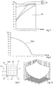
- the figure 7 represents the proportion of modes RL, GL, SGL, RGL and TGL as a function of the refractive index n encap of the encapsulation layer 34.
- the portion of light extracted from the light emitting diode is the sum of the parts RL and TGL.
- the figure 8 represents an evolution curve C RGL corresponding to the proportion of guided modes RGL on the total number of guided modes GL as a function of the refractive index n encap of the encapsulation layer 34.
- the curves of Figures 7 and 8 were obtained in the case of a hexagonal section GaN wire having an average diameter of 800 nm and a shell 275 nm thick.
- the proportion of entrapped guided light RGL decreases to zero for a refractive index of the encapsulation layer 34 equal to about 1.73.
- the inventors have demonstrated that the shape of the evolution curves of the proportions of modes RL, GL, SGL, RGL and TGL is substantially the same regardless of the average diameter of the wire 20, as soon as the average diameter of the wire 20 is greater than 200 nm.
- the refractive index at which the RGL propagation mode vanishes is substantially independent of the average diameter of the wire 20, as soon as the average diameter of the wire 20 is greater than 200 nm.
- the light must leave the encapsulation layer by the front face 36.
- the face 36 may correspond to a free surface, that is to say in contact with the air.
- the inventors have demonstrated by simulation that the best compromise was obtained with a refractive index of the encapsulation layer 34 between 1.7 and 1. , 75, preferably between 1.72 and 1.74, more preferably about 1.73.
- the mean diameter of the wire 20 is between 200 nm and 1 ⁇ m, preferably between 300 nm and 800 nm.
- the encapsulation layer 34 may comprise a matrix of an at least partially transparent inorganic material in which particles of a dielectric material are optionally distributed.
- the refractive index of the dielectric material composing the particles is strictly greater than the refractive index of the material composing the matrix.
- the encapsulation layer 34 comprises a matrix silicone, also called polysiloxane, and further comprises particles of a dielectric material distributed in the matrix.
- the particles are in any type of material making it possible to obtain particles of relatively spherical nanoscale dimensions and having a suitable refractive index.
- the particles may be made of titanium oxide (TiO 2 ), zirconium oxide (ZrO 2 ), zinc sulphide (ZnS), lead sulphide (PbS) or amorphous silicon (Si). .
- the average diameter of a particle is the diameter of the sphere of the same volume.
- the average particle diameter of the dielectric material is between 2 nm and 250 nm.
- the volume concentration of the particles relative to the total weight of the encapsulation layer 34 is between 1% and 50%.
- the inorganic material is chosen from the group comprising silicon oxides of the SiO x type where x is a real number strictly greater than 0 and less than or equal to 2, silicon oxides of the SiO y N z type where y is a real number strictly greater than 0 and less than or equal to 2 and z is strictly greater than 0 and less than or equal to 0.57, and aluminum oxide (Al 2 O 3 ).
- the encapsulation layer 34 may be made of at least partially transparent organic material.
- the encapsulation layer 34 is made of polyimide.
- the encapsulation layer 34 is an epoxy polymer which further comprises particles of a dielectric material distributed in the matrix. The particles can be made of titanium oxide (TiO 2 ), zirconium oxide (ZrO 2 ), zinc sulphide (ZnS), lead sulphide (PbS) or amorphous silicon (Si).
- a surface treatment can be applied to the face 36 of the encapsulation layer 34 so as to form reliefs on the face 36.
- the texturing process of the face 36 may comprise a step of chemical etching or mechanical abrasion step, optionally in the presence of a mask protecting treated portions of the face 36 to promote the formation of patterns on the surface.
- the texturing process of the face 36 may comprise a step of stamping, molding, etc.
- the encapsulation layer 34 may be covered with an additional layer at least partially transparent.
- the refractive index of the additional layer is then between the refractive index of the encapsulation layer 34 and the refractive index of the air.
- a stack of at least two layers may cover the encapsulation layer 34.
- the refractive indices of the layers of the stack are decreasing from the first layer of the stack in contact with the encapsulation layer 34 to the last layer of the stack in contact with the air, the refractive index of the first layer being strictly less than the refractive index of the encapsulation layer 34 and the refractive index of the last layer being strictly greater than the index of refraction of the air.
- the optoelectronic device according to the embodiment described above advantageously makes it possible to increase the overall extraction efficiency of the optoelectronic device, that is to say measured over the entire face 36.
- the extraction efficiency can be measured locally, that is to say for a portion of the face 36. It then corresponds to the ratio between the amount of light that escapes from the optoelectronic device by the portion in question and the quantity of light provided by the light-emitting diodes of this portion. It is desirable that variations in the local extraction efficiency over the entire face 36 be the lowest possible to prevent an observer perceives differences in luminance by looking at the optoelectronic device 5.
- the figure 9 is a view from above of an example of an optoelectronic device 50, comprising all the elements of the optoelectronic device 5 represented in FIG. figure 1 and wherein the LEDs are regularly distributed, for example in rows and columns, over a square active area 51.
- the side edges of the active area 51 are designated by the reference 52 and the corners of the active area 51 are designated 54.
- Each light emitting diode is schematically represented by a dot.
- each LED is located in the center of a square comprising a light emitting diode at each vertex and a light emitting diode in the middle of each edge.
- the density of light-emitting diodes per unit area is substantially constant over the entire active area 51.
- the surface density of light-emitting diodes is substantially constant and between 4 * 10 6 / cm 2 and 3 * 10 7 / cm 2 .
- the figure 10 represents the evolution of the local extraction efficiency of the optoelectronic device 50 of the figure 9 quarter of the active area 51.
- the curve of the figure 10 was obtained in the case of a matrix of GaN nanowires hexagonal section, the distance between the axes of two nanowires being 3 times the mean radius of the shell 28 and the refractive index of the material of the encapsulant 34 being equal to 1.75.
- the local extraction efficiency is greater along the edges 52 relative to the center of the active zone 51.
- the local extraction efficiency is greater than the vertices 54 with respect to the edges 52 of the active zone 51.
- the inventors have demonstrated a decrease in extraction efficiency as soon as the distance between the axes of two adjacent LEDs is less than 15 times the mean radius of the shell 28.
- the figure 11 is a view similar to the figure 9 of an embodiment of an optoelectronic device 60.
- the optoelectronic device 60 comprises all the elements of the optoelectronic device 50 with the difference that the density of light-emitting diodes per unit area increases gradually from the center of the device to the edges 52. More specifically, the surface density of light-emitting diodes in the center of the active area 51 is strictly less than the surface density of light-emitting diodes along the edges 52. In addition, the surface density of light-emitting diodes along the edges 52 is strictly less than the surface density of electroluminescent diodes at the vertices 54 of the active zone 51.
- the evolution of the surface density of light-emitting diodes may correspond to the inverse of the evolution of the extraction efficiency as represented in FIG. figure 10 .
- the surface density of light-emitting diodes in the center of the active zone of the optoelectronic device may be between 2 * 10 6 / cm 2 and 6 * 10 6 / cm 2 while the surface density of light-emitting diodes along an edge of the active area of the optoelectronic device may be between 7 * 10 6 / cm 2 and 2 * 10 7 / cm 2 .
- the inventors have demonstrated that the uniformity of extraction efficiency could be improved by increasing the ratio between the perimeter of the active zone and the surface of the active zone.
- the P / A ratio between the perimeter and the surface of the active zone is greater than 4 for a unit active area surface, preferably greater than or equal to 4.5, more preferably greater than or equal to 5, especially greater or equal to 6.
- FIGS 12 to 20 are schematic top views of embodiments of optoelectronic devices for each of which only the contour of the active area has been shown.
- the ratio between the perimeter of the active zone and the surface of the active zone is strictly greater than that obtained for a square of the same surface.
- the active zone 70 has an annular shape comprising a square outer edge 72 and a square inner edge 74.
- the active area 76 comprises one or more rectangular areas 78, with two rectangular areas being shown.
- the active area 80 comprises one or more of a strip 82 with wavy edges, two strips 82 being shown.
- the active zone 84 has a triangular shape.
- the active area 86 has a star shape.
- the active zone 88 comprises an outer edge 90 in the shape of a star and an inner edge 91 in the shape of a star.
- the outer perimeter, and possibly the inside, of the active zone follows a curve that is close to a fractal curve.
- the active areas 94, 96 and 98 are respectively in the form of a Koch flake after two, three and four iterations.
- the P / A ratio for a unit area of active area is 6.4, 8.5 and 11.4, respectively, for the active areas 94, 96 and 98.
- Figures 12 and 17 are examples of active areas corresponding to perforated surfaces.
- the insulating layer 26 covers the entire periphery of the lower portion 22 of each wire 20.
- a portion of the lower portion 22 may not be covered by the insulating layer 26.
- the insulating layer 26 covers the wire 20 to a height less than H 2 and the shell 28 covers the wire 20 to a height greater than H 3 .
- the layer 26 may not cover the lower portion 22 of each wire 20.
- the shell 28 may cover each wire 20 on the height H 1 .
- the insulating layer 26 does not cover the periphery of the upper portion 24 of each wire 20.
- the insulating layer 26 may cover a portion of the upper portion 24 of each wire 20.
- the insulating layer 26 covers the wire 20 to a height greater than H 2 and the shell 28 covers the wire 20 to a height less than H 3 .
- the insulating layer 26 may, for each wire 20, partly cover the lower portion of the shell 30.
- the layers composing the shell 28 may be formed before the insulating layer 26 on the whole of each wire 20 or only on a part of the wire 20, for example the upper part 24.
- each wire 20 comprises a passivated portion 22, at the base of the wire in contact with one of the seed pads 16, this passivated portion 22 may not be present.
- the shell 28 may be provided only at the top of the wire 20.
- the optoelectronic device comprising an encapsulation layer having a refractive index of between 1.7 and 1.75 may furthermore comprise a surface density of the light-emitting diodes which is variable, for example as represented in FIG. figure 11 .
- the optoelectronic device comprising an encapsulation layer having a refractive index of between 1.7 and 1.75 may also have a ratio between the perimeter and the surface of the active zone which is strictly greater than the ratio obtained for a square active area, for example as described above in relation to the Figures 12 to 20 .
- the optoelectronic device having a ratio between the perimeter and the surface of the active zone which is strictly greater than the ratio obtained for a square active zone may further comprise a variable density of the electroluminescent diodes.
Applications Claiming Priority (3)
| Application Number | Priority Date | Filing Date | Title |
|---|---|---|---|
| FR1363005A FR3015772B1 (fr) | 2013-12-19 | 2013-12-19 | Dispositif optoelectronique a diodes electroluminescentes a extraction de lumiere amelioree |
| EP14812451.4A EP3084846B1 (de) | 2013-12-19 | 2014-12-11 | Optoelektronische vorrichtung mit leuchtdioden mit verbesserter lichtextraktion |
| PCT/EP2014/077418 WO2015091212A1 (fr) | 2013-12-19 | 2014-12-11 | Dispositif optoelectronique a diodes electroluminescentes a extraction de lumiere amelioree |
Related Parent Applications (2)
| Application Number | Title | Priority Date | Filing Date |
|---|---|---|---|
| EP14812451.4A Division-Into EP3084846B1 (de) | 2013-12-19 | 2014-12-11 | Optoelektronische vorrichtung mit leuchtdioden mit verbesserter lichtextraktion |
| EP14812451.4A Division EP3084846B1 (de) | 2013-12-19 | 2014-12-11 | Optoelektronische vorrichtung mit leuchtdioden mit verbesserter lichtextraktion |
Publications (2)
| Publication Number | Publication Date |
|---|---|
| EP3373345A1 true EP3373345A1 (de) | 2018-09-12 |
| EP3373345B1 EP3373345B1 (de) | 2021-09-15 |
Family
ID=50102122
Family Applications (3)
| Application Number | Title | Priority Date | Filing Date |
|---|---|---|---|
| EP18169640.2A Active EP3373345B1 (de) | 2013-12-19 | 2014-12-11 | Optoelektronische vorrichtung mit leuchtdioden mit verbesserter lichtextraktion |
| EP18169638.6A Active EP3373344B1 (de) | 2013-12-19 | 2014-12-11 | Optoelektronische vorrichtung mit leuchtdioden mit verbesserter lichtextraktion |
| EP14812451.4A Active EP3084846B1 (de) | 2013-12-19 | 2014-12-11 | Optoelektronische vorrichtung mit leuchtdioden mit verbesserter lichtextraktion |
Family Applications After (2)
| Application Number | Title | Priority Date | Filing Date |
|---|---|---|---|
| EP18169638.6A Active EP3373344B1 (de) | 2013-12-19 | 2014-12-11 | Optoelektronische vorrichtung mit leuchtdioden mit verbesserter lichtextraktion |
| EP14812451.4A Active EP3084846B1 (de) | 2013-12-19 | 2014-12-11 | Optoelektronische vorrichtung mit leuchtdioden mit verbesserter lichtextraktion |
Country Status (8)
| Country | Link |
|---|---|
| US (3) | US9601543B2 (de) |
| EP (3) | EP3373345B1 (de) |
| JP (3) | JP6605472B2 (de) |
| KR (1) | KR102279462B1 (de) |
| CN (1) | CN106415858B (de) |
| FR (1) | FR3015772B1 (de) |
| TW (3) | TWI761708B (de) |
| WO (1) | WO2015091212A1 (de) |
Families Citing this family (10)
| Publication number | Priority date | Publication date | Assignee | Title |
|---|---|---|---|---|
| FR3015772B1 (fr) * | 2013-12-19 | 2017-10-13 | Aledia | Dispositif optoelectronique a diodes electroluminescentes a extraction de lumiere amelioree |
| FR3048817B1 (fr) * | 2016-03-11 | 2018-06-15 | Valeo Comfort And Driving Assistance | Ecran et afficheur tete haute comprenant un tel ecran |
| FR3053530B1 (fr) * | 2016-06-30 | 2018-07-27 | Aledia | Dispositif optoelectronique a pixels a contraste et luminance ameliores |
| FR3053436B1 (fr) * | 2016-07-01 | 2020-07-17 | Valeo Vision | Dispositif d'eclairage et/ou de signalisation pour vehicule automobile |
| JP7322064B2 (ja) * | 2018-04-25 | 2023-08-07 | コンコード (エイチケー) インターナショナル エデュケーション リミテッド | 誘電体層を有する反射画像ディスプレイのための装置及び方法 |
| TWI677110B (zh) * | 2018-05-14 | 2019-11-11 | 友達光電股份有限公司 | 微型發光二極體及發光裝置 |
| CN108807610B (zh) * | 2018-06-07 | 2019-12-20 | 台湾创界有限公司 | 微米led线性发光体的制备方法 |
| FR3082657B1 (fr) * | 2018-06-19 | 2021-01-29 | Aledia | Procede de fabrication d’un dispositif optoelectronique a parois de confinement lumineux auto alignes |
| GB2575311B (en) * | 2018-07-06 | 2021-03-03 | Plessey Semiconductors Ltd | Monolithic LED array and a precursor thereto |
| EP4139959A1 (de) * | 2020-04-20 | 2023-03-01 | Google LLC | Nanodraht-leuchtdioden mit gerichteter emission und anzeigen, die diese dioden beinhalten. |
Citations (1)
| Publication number | Priority date | Publication date | Assignee | Title |
|---|---|---|---|---|
| US20130313583A1 (en) * | 2012-05-22 | 2013-11-28 | Samsung Electronics Co., Ltd. | Light-emitting device and method of manufacturing the same |
Family Cites Families (26)
| Publication number | Priority date | Publication date | Assignee | Title |
|---|---|---|---|---|
| FR1363005A (fr) | 1963-07-13 | 1964-06-05 | Boehler & Co Ag Geb | Couronne de curetage |
| JP4160000B2 (ja) * | 2004-02-13 | 2008-10-01 | ドンゴク ユニバーシティ インダストリー アカデミック コーポレイション ファウンデイション | 発光ダイオードおよびその製造方法 |
| US20060091411A1 (en) * | 2004-10-29 | 2006-05-04 | Ouderkirk Andrew J | High brightness LED package |
| CN101084112A (zh) * | 2004-11-16 | 2007-12-05 | 奈米晶材照明有限公司 | 以光学上具有可靠的高折射率的纳米粒子为基础的纳米复合封装材料与光子波导材料 |
| JP2006310710A (ja) * | 2005-05-02 | 2006-11-09 | Sony Corp | 半導体発光素子 |
| WO2007001098A1 (en) * | 2005-06-25 | 2007-01-04 | Seoul Opto Device Co., Ltd. | Nanostructure having a nitride-based quantum well and light emitting diode employing the same |
| EP2126986B1 (de) * | 2006-12-22 | 2019-09-18 | QuNano AB | Led mit aufrechter nanodrahtstruktur und herstellungsverfahren dafür |
| US8183587B2 (en) * | 2006-12-22 | 2012-05-22 | Qunano Ab | LED with upstanding nanowire structure and method of producing such |
| JP2008244302A (ja) * | 2007-03-28 | 2008-10-09 | Matsushita Electric Works Ltd | 化合物半導体発光素子およびそれを用いる照明装置ならびに化合物半導体発光素子の製造方法 |
| FR2922685B1 (fr) * | 2007-10-22 | 2011-02-25 | Commissariat Energie Atomique | Dispositif optoelectronique a base de nanofils et procedes correspondants |
| JP2009147140A (ja) * | 2007-12-14 | 2009-07-02 | Panasonic Corp | 発光素子および発光素子の製造方法 |
| WO2010014032A1 (en) * | 2008-07-07 | 2010-02-04 | Glo Ab | A nanostructured LED |
| US20100123386A1 (en) * | 2008-11-13 | 2010-05-20 | Maven Optronics Corp. | Phosphor-Coated Light Extraction Structures for Phosphor-Converted Light Emitting Devices |
| JP5463901B2 (ja) * | 2009-12-24 | 2014-04-09 | 日亜化学工業株式会社 | 発光装置 |
| FR2975532B1 (fr) * | 2011-05-18 | 2013-05-10 | Commissariat Energie Atomique | Connexion electrique en serie de nanofils emetteurs de lumiere |
| KR101769075B1 (ko) * | 2010-12-24 | 2017-08-18 | 서울바이오시스 주식회사 | 발광 다이오드 칩 및 그것을 제조하는 방법 |
| JP2013055170A (ja) * | 2011-09-02 | 2013-03-21 | Sharp Corp | 自発光ディスプレイおよび自発光ディスプレイの製造方法 |
| US9204036B2 (en) | 2012-01-31 | 2015-12-01 | Fei Company | Image-enhancing spotlight mode for digital microscopy |
| JP5661671B2 (ja) * | 2012-03-26 | 2015-01-28 | 株式会社東芝 | 半導体発光素子 |
| TWI541992B (zh) * | 2012-05-14 | 2016-07-11 | 國立清華大學 | 發光二極體顯示器與其製造方法 |
| TWI489658B (zh) | 2012-05-25 | 2015-06-21 | Toshiba Kk | 半導體發光裝置及光源單元 |
| KR101891777B1 (ko) * | 2012-06-25 | 2018-08-24 | 삼성전자주식회사 | 유전체 리플렉터를 구비한 발광소자 및 그 제조방법 |
| US9190563B2 (en) * | 2013-11-25 | 2015-11-17 | Samsung Electronics Co., Ltd. | Nanostructure semiconductor light emitting device |
| FR3015772B1 (fr) | 2013-12-19 | 2017-10-13 | Aledia | Dispositif optoelectronique a diodes electroluminescentes a extraction de lumiere amelioree |
| DE102013114466A1 (de) * | 2013-12-19 | 2015-06-25 | Osram Gmbh | Optoelektronisches Halbleiterbauteil und Verfahren zur Herstellung eines optoelektronischen Halbleiterbauteils |
| KR102227771B1 (ko) * | 2014-08-25 | 2021-03-16 | 삼성전자주식회사 | 나노구조 반도체 발광소자 |
-
2013
- 2013-12-19 FR FR1363005A patent/FR3015772B1/fr not_active Expired - Fee Related
-
2014
- 2014-12-11 US US15/101,887 patent/US9601543B2/en active Active
- 2014-12-11 EP EP18169640.2A patent/EP3373345B1/de active Active
- 2014-12-11 EP EP18169638.6A patent/EP3373344B1/de active Active
- 2014-12-11 JP JP2016539256A patent/JP6605472B2/ja active Active
- 2014-12-11 CN CN201480069520.6A patent/CN106415858B/zh active Active
- 2014-12-11 EP EP14812451.4A patent/EP3084846B1/de active Active
- 2014-12-11 KR KR1020167016858A patent/KR102279462B1/ko active IP Right Grant
- 2014-12-11 WO PCT/EP2014/077418 patent/WO2015091212A1/fr active Application Filing
- 2014-12-16 TW TW108135841A patent/TWI761708B/zh active
- 2014-12-16 TW TW108102133A patent/TWI692886B/zh active
- 2014-12-16 TW TW103143892A patent/TWI656666B/zh active
-
2017
- 2017-02-07 US US15/426,690 patent/US10062818B2/en active Active
-
2018
- 2018-03-22 US US15/933,135 patent/US10177288B2/en active Active
-
2019
- 2019-06-18 JP JP2019113055A patent/JP2019169735A/ja active Pending
- 2019-06-18 JP JP2019113054A patent/JP6893954B2/ja active Active
Patent Citations (1)
| Publication number | Priority date | Publication date | Assignee | Title |
|---|---|---|---|---|
| US20130313583A1 (en) * | 2012-05-22 | 2013-11-28 | Samsung Electronics Co., Ltd. | Light-emitting device and method of manufacturing the same |
Non-Patent Citations (1)
| Title |
|---|
| JEN-HAU CHENG ET AL: "Atomic layer deposition enabled interconnect technology for vertical nanowire arrays", SENSORS AND ACTUATORS: A PHYSICAL ELSEVIER SEQUOIA S.A. SWITZERLAND, vol. 165, no. 1, January 2011 (2011-01-01), pages 107 - 114, XP002726521, ISSN: 0924-4247 * |
Also Published As
| Publication number | Publication date |
|---|---|
| US20180219143A1 (en) | 2018-08-02 |
| JP6605472B2 (ja) | 2019-11-13 |
| EP3084846B1 (de) | 2018-07-11 |
| CN106415858B (zh) | 2019-04-23 |
| JP2019169735A (ja) | 2019-10-03 |
| FR3015772A1 (fr) | 2015-06-26 |
| US10062818B2 (en) | 2018-08-28 |
| EP3373345B1 (de) | 2021-09-15 |
| TW201921736A (zh) | 2019-06-01 |
| TWI761708B (zh) | 2022-04-21 |
| KR102279462B1 (ko) | 2021-07-19 |
| FR3015772B1 (fr) | 2017-10-13 |
| JP2019195077A (ja) | 2019-11-07 |
| TW201535801A (zh) | 2015-09-16 |
| EP3373344A1 (de) | 2018-09-12 |
| CN106415858A (zh) | 2017-02-15 |
| TW202005123A (zh) | 2020-01-16 |
| JP6893954B2 (ja) | 2021-06-23 |
| EP3084846A1 (de) | 2016-10-26 |
| TWI692886B (zh) | 2020-05-01 |
| KR20160100983A (ko) | 2016-08-24 |
| TWI656666B (zh) | 2019-04-11 |
| US20160307960A1 (en) | 2016-10-20 |
| JP2017501573A (ja) | 2017-01-12 |
| WO2015091212A1 (fr) | 2015-06-25 |
| US10177288B2 (en) | 2019-01-08 |
| US9601543B2 (en) | 2017-03-21 |
| EP3373344B1 (de) | 2021-03-17 |
| US20170148960A1 (en) | 2017-05-25 |
Similar Documents
| Publication | Publication Date | Title |
|---|---|---|
| EP3084846B1 (de) | Optoelektronische vorrichtung mit leuchtdioden mit verbesserter lichtextraktion | |
| EP2911974B1 (de) | Optoelektronische vorrichtung und herstellungsverfahren dafür | |
| EP3401964B1 (de) | Optoelektronische vorrichtung mit elektrolumineszenzdioden | |
| EP3053195B1 (de) | Optoelektronische vorrichtung mit leuchtdioden | |
| EP2997605B1 (de) | Optoelektronische vorrichtung und herstellungsverfahren dafür | |
| EP3248227B1 (de) | Optoelektronisches halbleiterbauelement und herstellungsverfahren davon | |
| FR3061607A1 (fr) | Dispositif optoelectronique a diodes electroluminescentes | |
| EP3014665B1 (de) | Optoelektronische vorrichtung mit verbesserter reflexion und verfahren zu ihrer herstellung | |
| EP3090450B1 (de) | Optoelektronische vorrichtung mit halbleiterelementen und deren herstellungsverfahren | |
| EP2939276B1 (de) | Optoelektronisches bauteil mit mikrostäben oder nanostäben | |
| EP3164881B1 (de) | Optoelektronische vorrichtung mit halbleiterbauelementen und verfahren zur herstellung davon | |
| EP3646391A1 (de) | Optoelektronische vorrichtung | |
| EP3871255A1 (de) | Optoelektronische vorrichtung mit leuchtdioden mit verbesserter lichtextraktion | |
| WO2015097260A1 (fr) | Dispositif optoelectronique a diodes electroluminescentes a courant de fuite reduit | |
| FR3105878A1 (fr) | Dispositif à composants optoélectroniques tridimensionnels pour découpe au laser et procédé de découpe au laser d'un tel dispositif |
Legal Events
| Date | Code | Title | Description |
|---|---|---|---|
| PUAI | Public reference made under article 153(3) epc to a published international application that has entered the european phase |
Free format text: ORIGINAL CODE: 0009012 |
|
| STAA | Information on the status of an ep patent application or granted ep patent |
Free format text: STATUS: REQUEST FOR EXAMINATION WAS MADE |
|
| 17P | Request for examination filed |
Effective date: 20180426 |
|
| AC | Divisional application: reference to earlier application |
Ref document number: 3084846 Country of ref document: EP Kind code of ref document: P |
|
| AK | Designated contracting states |
Kind code of ref document: A1 Designated state(s): AL AT BE BG CH CY CZ DE DK EE ES FI FR GB GR HR HU IE IS IT LI LT LU LV MC MK MT NL NO PL PT RO RS SE SI SK SM TR |
|
| AX | Request for extension of the european patent |
Extension state: ME |
|
| STAA | Information on the status of an ep patent application or granted ep patent |
Free format text: STATUS: EXAMINATION IS IN PROGRESS |
|
| 17Q | First examination report despatched |
Effective date: 20200317 |
|
| STAA | Information on the status of an ep patent application or granted ep patent |
Free format text: STATUS: EXAMINATION IS IN PROGRESS |
|
| RAP1 | Party data changed (applicant data changed or rights of an application transferred) |
Owner name: ALEDIA Owner name: COMMISSARIAT A L'ENERGIE ATOMIQUE ET AUX ENERGIES ALTERNATIVES |
|
| GRAP | Despatch of communication of intention to grant a patent |
Free format text: ORIGINAL CODE: EPIDOSNIGR1 |
|
| STAA | Information on the status of an ep patent application or granted ep patent |
Free format text: STATUS: GRANT OF PATENT IS INTENDED |
|
| INTG | Intention to grant announced |
Effective date: 20210623 |
|
| GRAS | Grant fee paid |
Free format text: ORIGINAL CODE: EPIDOSNIGR3 |
|
| GRAA | (expected) grant |
Free format text: ORIGINAL CODE: 0009210 |
|
| STAA | Information on the status of an ep patent application or granted ep patent |
Free format text: STATUS: THE PATENT HAS BEEN GRANTED |
|
| AC | Divisional application: reference to earlier application |
Ref document number: 3084846 Country of ref document: EP Kind code of ref document: P |
|
| AK | Designated contracting states |
Kind code of ref document: B1 Designated state(s): AL AT BE BG CH CY CZ DE DK EE ES FI FR GB GR HR HU IE IS IT LI LT LU LV MC MK MT NL NO PL PT RO RS SE SI SK SM TR |
|
| REG | Reference to a national code |
Ref country code: CH Ref legal event code: EP |
|
| REG | Reference to a national code |
Ref country code: DE Ref legal event code: R096 Ref document number: 602014080205 Country of ref document: DE |
|
| REG | Reference to a national code |
Ref country code: IE Ref legal event code: FG4D Free format text: LANGUAGE OF EP DOCUMENT: FRENCH |
|
| REG | Reference to a national code |
Ref country code: AT Ref legal event code: REF Ref document number: 1431206 Country of ref document: AT Kind code of ref document: T Effective date: 20211015 |
|
| REG | Reference to a national code |
Ref country code: LT Ref legal event code: MG9D |
|
| REG | Reference to a national code |
Ref country code: NL Ref legal event code: MP Effective date: 20210915 |
|
| PG25 | Lapsed in a contracting state [announced via postgrant information from national office to epo] |
Ref country code: BG Free format text: LAPSE BECAUSE OF FAILURE TO SUBMIT A TRANSLATION OF THE DESCRIPTION OR TO PAY THE FEE WITHIN THE PRESCRIBED TIME-LIMIT Effective date: 20211215 Ref country code: LT Free format text: LAPSE BECAUSE OF FAILURE TO SUBMIT A TRANSLATION OF THE DESCRIPTION OR TO PAY THE FEE WITHIN THE PRESCRIBED TIME-LIMIT Effective date: 20210915 Ref country code: NO Free format text: LAPSE BECAUSE OF FAILURE TO SUBMIT A TRANSLATION OF THE DESCRIPTION OR TO PAY THE FEE WITHIN THE PRESCRIBED TIME-LIMIT Effective date: 20211215 Ref country code: RS Free format text: LAPSE BECAUSE OF FAILURE TO SUBMIT A TRANSLATION OF THE DESCRIPTION OR TO PAY THE FEE WITHIN THE PRESCRIBED TIME-LIMIT Effective date: 20210915 Ref country code: SE Free format text: LAPSE BECAUSE OF FAILURE TO SUBMIT A TRANSLATION OF THE DESCRIPTION OR TO PAY THE FEE WITHIN THE PRESCRIBED TIME-LIMIT Effective date: 20210915 Ref country code: HR Free format text: LAPSE BECAUSE OF FAILURE TO SUBMIT A TRANSLATION OF THE DESCRIPTION OR TO PAY THE FEE WITHIN THE PRESCRIBED TIME-LIMIT Effective date: 20210915 Ref country code: FI Free format text: LAPSE BECAUSE OF FAILURE TO SUBMIT A TRANSLATION OF THE DESCRIPTION OR TO PAY THE FEE WITHIN THE PRESCRIBED TIME-LIMIT Effective date: 20210915 |
|
| REG | Reference to a national code |
Ref country code: AT Ref legal event code: MK05 Ref document number: 1431206 Country of ref document: AT Kind code of ref document: T Effective date: 20210915 |
|
| PG25 | Lapsed in a contracting state [announced via postgrant information from national office to epo] |
Ref country code: LV Free format text: LAPSE BECAUSE OF FAILURE TO SUBMIT A TRANSLATION OF THE DESCRIPTION OR TO PAY THE FEE WITHIN THE PRESCRIBED TIME-LIMIT Effective date: 20210915 Ref country code: GR Free format text: LAPSE BECAUSE OF FAILURE TO SUBMIT A TRANSLATION OF THE DESCRIPTION OR TO PAY THE FEE WITHIN THE PRESCRIBED TIME-LIMIT Effective date: 20211216 |
|
| PG25 | Lapsed in a contracting state [announced via postgrant information from national office to epo] |
Ref country code: AT Free format text: LAPSE BECAUSE OF FAILURE TO SUBMIT A TRANSLATION OF THE DESCRIPTION OR TO PAY THE FEE WITHIN THE PRESCRIBED TIME-LIMIT Effective date: 20210915 |
|
| PG25 | Lapsed in a contracting state [announced via postgrant information from national office to epo] |
Ref country code: IS Free format text: LAPSE BECAUSE OF FAILURE TO SUBMIT A TRANSLATION OF THE DESCRIPTION OR TO PAY THE FEE WITHIN THE PRESCRIBED TIME-LIMIT Effective date: 20220115 Ref country code: SM Free format text: LAPSE BECAUSE OF FAILURE TO SUBMIT A TRANSLATION OF THE DESCRIPTION OR TO PAY THE FEE WITHIN THE PRESCRIBED TIME-LIMIT Effective date: 20210915 Ref country code: SK Free format text: LAPSE BECAUSE OF FAILURE TO SUBMIT A TRANSLATION OF THE DESCRIPTION OR TO PAY THE FEE WITHIN THE PRESCRIBED TIME-LIMIT Effective date: 20210915 Ref country code: RO Free format text: LAPSE BECAUSE OF FAILURE TO SUBMIT A TRANSLATION OF THE DESCRIPTION OR TO PAY THE FEE WITHIN THE PRESCRIBED TIME-LIMIT Effective date: 20210915 Ref country code: PT Free format text: LAPSE BECAUSE OF FAILURE TO SUBMIT A TRANSLATION OF THE DESCRIPTION OR TO PAY THE FEE WITHIN THE PRESCRIBED TIME-LIMIT Effective date: 20220117 Ref country code: PL Free format text: LAPSE BECAUSE OF FAILURE TO SUBMIT A TRANSLATION OF THE DESCRIPTION OR TO PAY THE FEE WITHIN THE PRESCRIBED TIME-LIMIT Effective date: 20210915 Ref country code: NL Free format text: LAPSE BECAUSE OF FAILURE TO SUBMIT A TRANSLATION OF THE DESCRIPTION OR TO PAY THE FEE WITHIN THE PRESCRIBED TIME-LIMIT Effective date: 20210915 Ref country code: ES Free format text: LAPSE BECAUSE OF FAILURE TO SUBMIT A TRANSLATION OF THE DESCRIPTION OR TO PAY THE FEE WITHIN THE PRESCRIBED TIME-LIMIT Effective date: 20210915 Ref country code: EE Free format text: LAPSE BECAUSE OF FAILURE TO SUBMIT A TRANSLATION OF THE DESCRIPTION OR TO PAY THE FEE WITHIN THE PRESCRIBED TIME-LIMIT Effective date: 20210915 Ref country code: CZ Free format text: LAPSE BECAUSE OF FAILURE TO SUBMIT A TRANSLATION OF THE DESCRIPTION OR TO PAY THE FEE WITHIN THE PRESCRIBED TIME-LIMIT Effective date: 20210915 Ref country code: AL Free format text: LAPSE BECAUSE OF FAILURE TO SUBMIT A TRANSLATION OF THE DESCRIPTION OR TO PAY THE FEE WITHIN THE PRESCRIBED TIME-LIMIT Effective date: 20210915 |
|
| REG | Reference to a national code |
Ref country code: DE Ref legal event code: R097 Ref document number: 602014080205 Country of ref document: DE |
|
| PLBE | No opposition filed within time limit |
Free format text: ORIGINAL CODE: 0009261 |
|
| STAA | Information on the status of an ep patent application or granted ep patent |
Free format text: STATUS: NO OPPOSITION FILED WITHIN TIME LIMIT |
|
| PG25 | Lapsed in a contracting state [announced via postgrant information from national office to epo] |
Ref country code: MC Free format text: LAPSE BECAUSE OF FAILURE TO SUBMIT A TRANSLATION OF THE DESCRIPTION OR TO PAY THE FEE WITHIN THE PRESCRIBED TIME-LIMIT Effective date: 20210915 Ref country code: DK Free format text: LAPSE BECAUSE OF FAILURE TO SUBMIT A TRANSLATION OF THE DESCRIPTION OR TO PAY THE FEE WITHIN THE PRESCRIBED TIME-LIMIT Effective date: 20210915 |
|
| REG | Reference to a national code |
Ref country code: CH Ref legal event code: PL |
|
| 26N | No opposition filed |
Effective date: 20220616 |
|
| PG25 | Lapsed in a contracting state [announced via postgrant information from national office to epo] |
Ref country code: SI Free format text: LAPSE BECAUSE OF FAILURE TO SUBMIT A TRANSLATION OF THE DESCRIPTION OR TO PAY THE FEE WITHIN THE PRESCRIBED TIME-LIMIT Effective date: 20210915 |
|
| REG | Reference to a national code |
Ref country code: BE Ref legal event code: MM Effective date: 20211231 |
|
| PG25 | Lapsed in a contracting state [announced via postgrant information from national office to epo] |
Ref country code: LU Free format text: LAPSE BECAUSE OF NON-PAYMENT OF DUE FEES Effective date: 20211211 Ref country code: IE Free format text: LAPSE BECAUSE OF NON-PAYMENT OF DUE FEES Effective date: 20211211 |
|
| PG25 | Lapsed in a contracting state [announced via postgrant information from national office to epo] |
Ref country code: BE Free format text: LAPSE BECAUSE OF NON-PAYMENT OF DUE FEES Effective date: 20211231 |
|
| PG25 | Lapsed in a contracting state [announced via postgrant information from national office to epo] |
Ref country code: LI Free format text: LAPSE BECAUSE OF NON-PAYMENT OF DUE FEES Effective date: 20211231 Ref country code: CH Free format text: LAPSE BECAUSE OF NON-PAYMENT OF DUE FEES Effective date: 20211231 |
|
| PG25 | Lapsed in a contracting state [announced via postgrant information from national office to epo] |
Ref country code: IT Free format text: LAPSE BECAUSE OF FAILURE TO SUBMIT A TRANSLATION OF THE DESCRIPTION OR TO PAY THE FEE WITHIN THE PRESCRIBED TIME-LIMIT Effective date: 20210915 |
|
| PG25 | Lapsed in a contracting state [announced via postgrant information from national office to epo] |
Ref country code: HU Free format text: LAPSE BECAUSE OF FAILURE TO SUBMIT A TRANSLATION OF THE DESCRIPTION OR TO PAY THE FEE WITHIN THE PRESCRIBED TIME-LIMIT; INVALID AB INITIO Effective date: 20141211 |
|
| PG25 | Lapsed in a contracting state [announced via postgrant information from national office to epo] |
Ref country code: CY Free format text: LAPSE BECAUSE OF FAILURE TO SUBMIT A TRANSLATION OF THE DESCRIPTION OR TO PAY THE FEE WITHIN THE PRESCRIBED TIME-LIMIT Effective date: 20210915 |
|
| PGFP | Annual fee paid to national office [announced via postgrant information from national office to epo] |
Ref country code: GB Payment date: 20231221 Year of fee payment: 10 |
|
| PGFP | Annual fee paid to national office [announced via postgrant information from national office to epo] |
Ref country code: FR Payment date: 20231228 Year of fee payment: 10 Ref country code: DE Payment date: 20231208 Year of fee payment: 10 |
|
| PG25 | Lapsed in a contracting state [announced via postgrant information from national office to epo] |
Ref country code: MK Free format text: LAPSE BECAUSE OF FAILURE TO SUBMIT A TRANSLATION OF THE DESCRIPTION OR TO PAY THE FEE WITHIN THE PRESCRIBED TIME-LIMIT Effective date: 20210915 |