EP3370274B1 - Organisches lichtemittierendes element - Google Patents
Organisches lichtemittierendes element Download PDFInfo
- Publication number
- EP3370274B1 EP3370274B1 EP16860212.6A EP16860212A EP3370274B1 EP 3370274 B1 EP3370274 B1 EP 3370274B1 EP 16860212 A EP16860212 A EP 16860212A EP 3370274 B1 EP3370274 B1 EP 3370274B1
- Authority
- EP
- European Patent Office
- Prior art keywords
- light emitting
- emitting device
- layer
- organic light
- reflection reducing
- Prior art date
- Legal status (The legal status is an assumption and is not a legal conclusion. Google has not performed a legal analysis and makes no representation as to the accuracy of the status listed.)
- Active
Links
Images

Classifications
-
- H—ELECTRICITY
- H10—SEMICONDUCTOR DEVICES; ELECTRIC SOLID-STATE DEVICES NOT OTHERWISE PROVIDED FOR
- H10K—ORGANIC ELECTRIC SOLID-STATE DEVICES
- H10K59/00—Integrated devices, or assemblies of multiple devices, comprising at least one organic light-emitting element covered by group H10K50/00
- H10K59/80—Constructional details
- H10K59/805—Electrodes
-
- G—PHYSICS
- G02—OPTICS
- G02B—OPTICAL ELEMENTS, SYSTEMS OR APPARATUS
- G02B5/00—Optical elements other than lenses
- G02B5/30—Polarising elements
- G02B5/3025—Polarisers, i.e. arrangements capable of producing a definite output polarisation state from an unpolarised input state
-
- H—ELECTRICITY
- H10—SEMICONDUCTOR DEVICES; ELECTRIC SOLID-STATE DEVICES NOT OTHERWISE PROVIDED FOR
- H10K—ORGANIC ELECTRIC SOLID-STATE DEVICES
- H10K50/00—Organic light-emitting devices
- H10K50/80—Constructional details
- H10K50/805—Electrodes
-
- H—ELECTRICITY
- H10—SEMICONDUCTOR DEVICES; ELECTRIC SOLID-STATE DEVICES NOT OTHERWISE PROVIDED FOR
- H10K—ORGANIC ELECTRIC SOLID-STATE DEVICES
- H10K50/00—Organic light-emitting devices
- H10K50/80—Constructional details
- H10K50/86—Arrangements for improving contrast, e.g. preventing reflection of ambient light
-
- H—ELECTRICITY
- H10—SEMICONDUCTOR DEVICES; ELECTRIC SOLID-STATE DEVICES NOT OTHERWISE PROVIDED FOR
- H10K—ORGANIC ELECTRIC SOLID-STATE DEVICES
- H10K59/00—Integrated devices, or assemblies of multiple devices, comprising at least one organic light-emitting element covered by group H10K50/00
- H10K59/30—Devices specially adapted for multicolour light emission
-
- H—ELECTRICITY
- H10—SEMICONDUCTOR DEVICES; ELECTRIC SOLID-STATE DEVICES NOT OTHERWISE PROVIDED FOR
- H10K—ORGANIC ELECTRIC SOLID-STATE DEVICES
- H10K50/00—Organic light-emitting devices
- H10K50/80—Constructional details
- H10K50/86—Arrangements for improving contrast, e.g. preventing reflection of ambient light
- H10K50/865—Arrangements for improving contrast, e.g. preventing reflection of ambient light comprising light absorbing layers, e.g. light-blocking layers
-
- H—ELECTRICITY
- H10—SEMICONDUCTOR DEVICES; ELECTRIC SOLID-STATE DEVICES NOT OTHERWISE PROVIDED FOR
- H10K—ORGANIC ELECTRIC SOLID-STATE DEVICES
- H10K59/00—Integrated devices, or assemblies of multiple devices, comprising at least one organic light-emitting element covered by group H10K50/00
-
- H—ELECTRICITY
- H10—SEMICONDUCTOR DEVICES; ELECTRIC SOLID-STATE DEVICES NOT OTHERWISE PROVIDED FOR
- H10K—ORGANIC ELECTRIC SOLID-STATE DEVICES
- H10K59/00—Integrated devices, or assemblies of multiple devices, comprising at least one organic light-emitting element covered by group H10K50/00
- H10K59/80—Constructional details
-
- H—ELECTRICITY
- H10—SEMICONDUCTOR DEVICES; ELECTRIC SOLID-STATE DEVICES NOT OTHERWISE PROVIDED FOR
- H10K—ORGANIC ELECTRIC SOLID-STATE DEVICES
- H10K59/00—Integrated devices, or assemblies of multiple devices, comprising at least one organic light-emitting element covered by group H10K50/00
- H10K59/80—Constructional details
- H10K59/805—Electrodes
- H10K59/8052—Cathodes
- H10K59/80524—Transparent cathodes, e.g. comprising thin metal layers
-
- H—ELECTRICITY
- H10—SEMICONDUCTOR DEVICES; ELECTRIC SOLID-STATE DEVICES NOT OTHERWISE PROVIDED FOR
- H10K—ORGANIC ELECTRIC SOLID-STATE DEVICES
- H10K59/00—Integrated devices, or assemblies of multiple devices, comprising at least one organic light-emitting element covered by group H10K50/00
- H10K59/80—Constructional details
- H10K59/8791—Arrangements for improving contrast, e.g. preventing reflection of ambient light
- H10K59/8792—Arrangements for improving contrast, e.g. preventing reflection of ambient light comprising light absorbing layers, e.g. black layers
Definitions
- the present specification relates to an organic light emitting device.
- An organic light emitting phenomenon refers to a phenomenon of converting electrical energy to light energy using an organic material. That is, when an appropriate organic material layer is positioned between an anode and a cathode, and voltage is applied between two electrodes, holes are injected into the organic material layer from the anode and electrons are injected into the organic material layer from the cathode. Exciton is generated when the injected holes and electrons encounter, and light is generated when the exciton falls down to a bottom state.
- a metal electrode having high reflectance used in an organic light emitting device provides a surface, which reflects internally generated light in a direction of a light transmissive substrate, thereby assisting in the improvement of brightness.
- the metal electrode reflects peripheral light incident to an element structure through the light transmissive substrate and a light transmissive electrode, thereby degrading contrast of light emission recognized with the eyes when an observer views the reflected light.
- a method of additionally introducing a polarizing plate to the light transmissive substrate may be used.
- light generated in an organic emission layer is also blocked, in order to exhibit higher efficiency, power is increased and used, so that the amount of power consumed of the organic light emitting device is increased and a life of the organic light emitting device is decreased.
- Document US 2007/170841 A1 discloses an OLED with one of the electrodes comprising a metal oxide as antireflective coating (ARC).
- Documents US 2013/140065 A1 , EP 2 767 985 A1 , US 2007/030569 and US 2016/056311 A1 disclose the possibility of using in a display an ARC comprising AlON.
- the present specification provides an organic light emitting device, which is capable of decreasing reflection of external light.
- the organic light emitting device may implement excellent contrast by controlling reflection of external light.
- the organic light emitting device does not need to include a polarizing plate for blocking reflection of external light, thereby implementing excellent brightness with lower power.
- An organic light emitting device is operable only when holes and electrons smoothly move between an anode, a cathode, and respective layers provided between the anode and the cathode. When an energy relationship of any one layer is not matched with an adjacent layer, the organic light emitting device may not be operated.
- the present inventors completed the present invention as a result of the repeated conduction of research on a material and a position of a light reflection reducing layer, which prevents reflection of a metal electrode according to external light, and enables an organic light emitting device to be operable.
- the present inventors found that when a light reflection reducing layer including an aluminum oxynitride is formed at a contact position with a metal electrode, it is possible to control reflection of external light by the metal electrode, and further, there is no problem in operating an organic light emitting device.
- FIG. 1 illustrates an example of a laminated structure of an organic light emitting device according to an exemplary embodiment of the present specification. Particularly, FIG. 1 illustrates an organic light emitting device, in which a transparent electrode 100, an organic material layer 300, a light reflection reducing layer 400, and a metal electrode 200 are sequentially provided.
- the organic light emitting device according to the exemplary embodiment of the present specification is not limited to the structure of FIG. 1 , and an additional layer may be further provided.
- the difference in work function between the metal electrode and the light reflection reducing layer is 0 eV or more and 1.4 eV or less.
- an energy barrier of the metal electrode and the electron transporting layer is about 1.4 eV, so that a difference in a work function between the metal electrode and the light reflection reducing layer is 0 eV or more and 1.4 eV or less, and for example, a difference in a work function may be 0 eV or more and 0.5 eV or less, or 0 eV or more and 0.2 eV or less.
- the organic light emitting device when the difference in the work function between the metal electrode and the light reflection reducing layer is within the range, the organic light emitting device may be smoothly operated.
- an energy relationship between the respective layers is important, so that when the difference in the work function deviates from the range, there is a problem in that efficiency of the organic light emitting device is sharply degraded, or the organic light emitting device may not be operated.
- the work function of the light reflection reducing layer is 3.5 eV or more and 4.2 eV or less.
- the light reflection reducing layer includes an aluminum oxynitride expressed with Al x O y N z and x is at% of aluminum and has a value of 55 to 65, y is at% of oxygen and has a value of 1 to 10, and z is at% of nitrogen, and has a value of 30 to 40.
- the metal electrode may include one or two or more metals selected from the group consisting of Cu, Al, Mo, Ti, Ag, Ni, Mn, Au, Cr, and Co.
- the metal electrode may be a metal electrode including Al as a main material. More particularly, according to the exemplary embodiment of the present specification, the metal electrode may be formed of Al.
- the thickness of the light reflection reducing layer is 20 mm or more and 60 nm or less.
- the light reflection reducing layer may have a color in the achromatic series, but the color thereof is not particularly limited thereto.
- the color in the achromatic color series means a color that does not selectively absorb light incident to a surface of an object and appears when the light is evenly reflected and absorbed with respect to a wavelength of each component.
- the organic light emitting device may further include a second metal layer, which is in contact with a surface of the light reflection reducing layer facing the transparent electrode and has a thickness of less than 10 nm.
- a thickness of the metal layer may be 5 nm or less.
- FIG. 2 illustrates an example of a laminated structure of an organic light emitting device according to an exemplary embodiment of the present specification. Particularly, FIG. 2 illustrates an organic light emitting device, in which a transparent electrode 100, an organic material layer 300, a metal layer 500, a light reflection reducing layer 400, and a metal electrode 200 are sequentially provided.
- the organic light emitting device according to the exemplary embodiment of the present specification is not limited to the structure of FIG. 2 , and an additional layer may be further provided.
- the metal layer is provided between the light reflection reducing layer and the adjacent layer to help electrons to more smoothly move.
- the metal layer may be transparent or translucent.
- the metal layer is formed of a thin film having a thickness of less than 10 nm, so that the metal layer is transparent or opaque, and according to an addition of the metal layer, light reflectance in the surface of the transparent electrode may be partially increased, but an electric characteristic of the organic light emitting device may be improved.
- transparent in the present specification means that light reflectance in a visible ray region is 50% or more, 70% or more, or 80% or more.
- translucent in the present specification means that light reflectance in a visible ray region is 20 % or more, 30 % or more, or 40 % or more.
- an extinction coefficient k of the light reflection reducing layer may be 0.04 or more and 1.3 or less in light having a wavelength of 550 nm.
- the extinction coefficient is within the range, it is possible to effectively control light reflectance of the metal electrode, thereby further improving visibility of the organic light emitting device.
- the extinction coefficient may be measured by using the Ellipsometer measurement equipment, which is known in the art.
- the extinction coefficient k may also be called an absorption coefficient, and is an index defining how strong a target material absorbs light at a predetermined wavelength. Accordingly, the incident light passes through the light reflection reducing layer having the thickness t and is firstly absorbed according to the degree of extinction coefficient k, and the light reflected by the electrode layer in the lower portion of the light reflection reducing layer passes through the light reflection reducing layer having the thickness t again and is secondarily absorbed, and then is externally reflected. Accordingly, the thickness of the light reflection reducing layer and the value of the absorption coefficient act as the important factors influencing the entire reflectance.
- a refractive index n of the light reflection reducing layer may be 2 or more and 3 or less in light having a wavelength of 550 nm.
- the first reflection occurs in a material of the light reflection reducing layer having the refractive index n together with the extinction coefficient k, and in this case, the main factors determining the first reflection are the refractive index n and the absorption coefficient k. Accordingly, the refractive index n and the absorption coefficient k are closely related to each other, and the effect may be maximized within the range.
- light reflectance in the surface of the transparent electrode may be 20 % or less in light having a wavelength of 550 nm.
- light reflectance in the surface of the light reflection reducing layer provided on the metal electrode may be 20% or less, 15% or less, or 10% or less in light having a wavelength of 550 nm.
- the light reflection reducing layer is provided on the metal electrode and considerably decreases light reflectance of the surface of the metal electrode by external light, thereby enabling the organic light emitting device to implement clearer colors.
- the transparent electrode or the metal electrode may be provided on a substrate.
- FIG. 3 illustrates an example of a laminated structure of an organic light emitting device according to an exemplary embodiment of the present specification. Particularly, FIG. 3 illustrates an organic light emitting device, in which a substrate 600, a transparent electrode 100, an organic material layer 300, a light reflection reducing layer 400, and a metal electrode 200 are sequentially provided.
- the organic light emitting device according to the exemplary embodiment of the present specification is not limited to the structure of FIG. 3 , and an additional layer may be further provided.
- FIG. 4 illustrates an example of a laminated structure of an organic light emitting device according to an exemplary embodiment of the present specification.
- FIG. 4 illustrates an organic light emitting device, in which a substrate 600, a metal electrode 200, a light reflection reducing layer 400, an organic material layer 300, and a transparent electrode 100 are sequentially provided.
- the organic light emitting device according to the exemplary embodiment of the present specification is not limited to the structure of FIG. 4 , and an additional layer may be further provided.
- light generated in the organic material layer 300 is extracted through the transparent electrode 200, not the substrate 600, and the light reflection reducing layer 400 controls reflection of external light incident from the transparent electrode 100.
- a substrate having excellent transparency, surface flatness, treatment easiness, and waterproofing property may be used as the substrate.
- a glass substrate, a thin glass substrate, or a transparent plastic substrate may be used as the substrate.
- a film of polyethylene terephthalate (PET), polyethylene naphthalate (PEN), polyether ether ketone (PEEK), and polyimide (PI) may be included as the plastic substrate in a form of a single layer or a multilayer.
- the substrate itself may include a light scattering function.
- the substrate is not limited thereto, and a substrate generally used in the organic light emitting device may be used.
- the transparent electrode includes: a metal, such as vanadium, chromium, copper, zinc and gold, or an alloy thereof; a metal oxide, such as zinc oxide, indium oxide, indium tin oxide (ITO), and indium zinc oxide (IZO); a combination of a metal and an oxide, such as ZnO:Al or SnO 2 :Sb; a conductive polymer, such as poly(3-methylthiophene), poly[3,4-(ethylene-1,2-dioxy)thiophene] (PEDT), polypyrrole, and polyaniline; and the like, but is not limited thereto.
- a metal such as vanadium, chromium, copper, zinc and gold, or an alloy thereof
- a metal oxide such as zinc oxide, indium oxide, indium tin oxide (ITO), and indium zinc oxide (IZO)
- IZO indium zinc oxide
- a combination of a metal and an oxide such as ZnO:Al or SnO 2 :Sb
- the transparent electrode may be an anode and the metal electrode may be a cathode. Further, the transparent electrode may be a cathode, and the metal electrode may be an anode.
- the organic material layer may include one or more emission layers, and may further include one or two or more selected from the group consisting of a hole injection layer, a hole transporting layer, a hole blocking layer, a charge generating layer, an electron blocking layer, an electron transporting layer, and an electron injection layer.
- the charge generating layer refers to a layer, in which holes and electrons are generated when a voltage is applied.
- a material which is capable of receiving holes from the anode or the hole injection layer and transferring the received holes to an emission layer, and has high mobility for holes, is suitable as a material of the hole transporting layer according to the present specification.
- the material of the hole transporting layer include an arylamine-based organic material, a conductive polymer, and a block copolymer in which a conjugate portion and a non-conjugate portion are simultaneously included, but are not limited thereto.
- a material of the emission layer according to the present specification may be a material, which is capable of emitting light in a visible ray region by receiving holes and electrons from the hole transporting layer and the electron transporting layer, respectively, and combining the holes and the electrons, and has excellent quantum efficiency to fluorescent or phosphorescence.
- the material of the emission layer include 8-hydroxy-quinoline-aluminum complex (Alq 3 ), carbazole-based compounds, dimerized styryl compounds, BAlq; 10-hydroxybenzoquinoline-metal compounds, benzoxazole-based, benzthiazole-based and benzimidazole-based compounds, poly(p-phenylenevinylene)(PPV)-based polymers, spiro compounds, polyfluorene, rubrene, and the like, but the material of the emission layer is not limited thereto.
- Alq 3 8-hydroxy-quinoline-aluminum complex
- carbazole-based compounds dimerized styryl compounds
- BAlq 10-hydroxybenzoquinoline-metal compounds
- benzoxazole-based benzoxazole-based
- benzthiazole-based and benzimidazole-based compounds poly(p-phenylenevinylene)(PPV)-based polymers
- spiro compounds polyfluorene,
- a material which is capable of accepting and transferring electrons from the cathode to the emission layer, and has high mobility to electrons, is suitable as the material of the electron transporting layer according to the present specification.
- Particular examples of the material of the electron transporting layer include a 8-hydroxyquinoline Al complex; a complex including Alq 3 ; an organic radical compound; a hydroxyflavone metal complex, and the like, but are not limited thereto.
- An exemplary embodiment of the present specification provides a display device including the organic light emitting device.
- the organic light emitting device may serve as a back light in the display device. Further, the organic light emitting device may serve as an emission layer of a pixel unit in the display device. Configurations known in the art may be applied as the configurations necessary for the display device.
- the present inventors reviewed whether electrons move in the structure, in which the electron transporting layer, the light reflection reducing layer, and the metal electrode are sequentially laminated.
- an organic light emitting device in which Alq is used as the electron transporting layer, Al 60 N 35 O 5 is used as the light reflection reducing layer, and Al is used as the metal electrode, was modelled. The modelling was performed through the ab initio density functional theory calculating method.
- a work function W may be defined as described below.
- W ⁇ e ⁇ ⁇ EF
- a work function is minimum energy required for removing free electrons from a material.
- a Fermi Level (EF) of Al 60 N 35 O 5 is 0.2025 eV, and when a work function is calculated through the definition of the work function by using the Fermi Level (EF) of Al 60 N 35 O 5 , a work function of is Al 60 N 35 O 5 is 3.8975 eV.
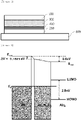
- FIG. 5 illustrates an energy relationship between respective layers according to Example 1.
- Different materials have different Fermi levels, and also have different work functions. When two materials are away from each other, the two materials have unique values, but when two materials are close and bonded to each other, the Fermi levels of the heterogeneous materials are arranged by a movement of free electrons. Accordingly, a junction of a metal and a metal or a metal and a semiconductor has the same Fermi level.
- the work function of Al is known as 4.08 eV, and a difference in a work function between Al and Al 60 N 35 O 5 is 0.1825 eV, and an interlayer energy barrier is low, so that there is no problem in the movement of the charges. Further, it can be seen that there is no problem in the movement of the charges from to LUMO of Alq.
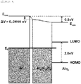
- an organic light emitting device in which Alq is used as the electron transporting layer, Al 58 N 38 O 4 is used as the light reflection reducing layer, and Al is used as the metal electrode, was modelled.
- a Fermi Level (EF) of Al 58 N 38 O 4 is -0.1444 eV, and when a work function is calculated through the definition of the work function by using the Fermi Level (EF) of Al 60 N 35 O 5 , a work function of is Al 58 N 38 O 4 is 4.0144 eV.
- FIG. 6 illustrates an energy relationship between respective layers according to Example 2.
- the work function of Al is known as 4.08 eV, and a difference in a work function between Al and Al 58 N 38 O 4 is 0.0656 eV, and an interlayer energy barrier is low, so that there is no problem in the movement of the charges. Further, it can be seen that there is no problem in the movement of the charges from Al 58 N 38 O 4 to LUMO of Alq.
Landscapes
- Physics & Mathematics (AREA)
- Optics & Photonics (AREA)
- General Physics & Mathematics (AREA)
- Electroluminescent Light Sources (AREA)
- Devices For Indicating Variable Information By Combining Individual Elements (AREA)
Claims (7)
- Organische lichtemittierende Vorrichtung, umfassend:eine transparente Elektrode (100);eine Metallelektrode (200), die bereitgestellt ist, um der transparenten Elektrode (100) gegenüberzuliegen;eine oder mehrere organische Materialschichten (300), die zwischen der transparenten Elektrode (100) und der Metallelektrode (200) bereitgestellt ist bzw. sind;eine Lichtreflektionsreduzierungsschicht (400), die zwischen der Metallelektrode (200) und der einen oder den mehreren organischen Materialschichten (300) bereitgestellt ist und mit der Oberfläche der Metallelektrode (200), die der transparenten Elektrode (100) gegenüberliegt, in Kontakt ist,wobei die organische Materialschicht (300) eine oder mehrere Emissionsschichten einschließt, wobei die organische lichtemittierende Vorrichtung dadurch gekennzeichnet ist, dass die Lichtreflektionsreduzierungsschicht (400) ein Aluminiumoxynitrid einschließt, das als AlxOyNz ausgedrückt ist, wobeix Atom% von Aluminium ist und einen Wert von 55 bis 65 aufweist,y Atom% von Sauerstoff ist und einen Wert von 1 bis 10 aufweist, undz Atom% von Stickstoff ist und einen Wert von 30 bis 40 aufweist,wobei der Unterschied in der Arbeitsfunktion zwischen der Metallelektrode (200) und der Lichtreflektionsreduzierungsschicht (400) o eV oder mehr und 1,4 eV oder weniger ist,die Arbeitsfunktion der Lichtreflektionsreduzierungsschicht (400) 3,5 eV oder mehr und 4,2 eV oder weniger ist, unddie Dicke der Lichtreflektionsreduzierungsschicht (400) 20 nm oder mehr und 60 nm oder weniger ist.
- Organische lichtemittierende Vorrichtung nach Anspruch 1, wobei die Metallelektrode (200) ein oder zwei oder mehr Metalle einschließt, die ausgewählt sind aus der Gruppe bestehend aus Cu, Al, Mo, Ti, Ag, Ni, Mn, Au, Cr und Co.
- Organische lichtemittierende Vorrichtung nach Anspruch 1, weiter umfassend:eine zweite Metallschicht (500), die zwischen der Lichtreflektionsreduzierungsschicht (400) und der einen oder den mehreren organischen Materialschichten (300) bereitgestellt ist, und die in Kontakt ist mit der Oberfläche der Lichtreflektionsreduzierungsschicht (400), die der transparenten Elektrode (100) gegenüberliegt, und die eine Dicke von weniger als 10 nm aufweist,wobei die zweite Metallschicht (500) transparent oder transluzent ist.
- Organische lichtemittierende Vorrichtung nach Anspruch 1, wobei ein Extinktionskoeffizient (k) der Lichtreflektionsreduzierungsschicht (400) 0,04 oder mehr und 1,3 oder weniger bei Licht einer Wellenlänge von 550 nm ist.
- Organische lichtemittierende Vorrichtung nach Anspruch 1, wobei ein Brechungsindex (n) der Lichtreflektionsreduzierungsschicht (400) 2 oder mehr und 3 oder weniger bei Licht einer Wellenlänge von 550 nm ist.
- Organische lichtemittierende Vorrichtung nach Anspruch 1, wobei die transparente Elektrode (100) oder die Metallelektrode (200) auf einem Substrat (600) bereitgestellt ist.
- Anzeigevorrichtung, die die organische lichtemittierende Vorrichtung nach einem der Ansprüche 1 bis 6 einschließt.
Applications Claiming Priority (2)
| Application Number | Priority Date | Filing Date | Title |
|---|---|---|---|
| KR1020150149503A KR102010401B1 (ko) | 2015-10-27 | 2015-10-27 | 유기발광소자 |
| PCT/KR2016/012097 WO2017074029A1 (ko) | 2015-10-27 | 2016-10-26 | 유기발광소자 |
Publications (3)
| Publication Number | Publication Date |
|---|---|
| EP3370274A1 EP3370274A1 (de) | 2018-09-05 |
| EP3370274A4 EP3370274A4 (de) | 2018-10-31 |
| EP3370274B1 true EP3370274B1 (de) | 2022-10-12 |
Family
ID=58630575
Family Applications (1)
| Application Number | Title | Priority Date | Filing Date |
|---|---|---|---|
| EP16860212.6A Active EP3370274B1 (de) | 2015-10-27 | 2016-10-26 | Organisches lichtemittierendes element |
Country Status (7)
| Country | Link |
|---|---|
| US (1) | US20180269420A1 (de) |
| EP (1) | EP3370274B1 (de) |
| JP (1) | JP6541089B2 (de) |
| KR (1) | KR102010401B1 (de) |
| CN (1) | CN108140742A (de) |
| TW (1) | TWI699921B (de) |
| WO (1) | WO2017074029A1 (de) |
Families Citing this family (1)
| Publication number | Priority date | Publication date | Assignee | Title |
|---|---|---|---|---|
| CN111864105A (zh) * | 2020-07-09 | 2020-10-30 | 武汉华星光电半导体显示技术有限公司 | 显示面板及其制备方法 |
Family Cites Families (16)
| Publication number | Priority date | Publication date | Assignee | Title |
|---|---|---|---|---|
| JP2000021860A (ja) * | 1998-07-03 | 2000-01-21 | Hitachi Ltd | 半導体装置およびその製造方法 |
| US6429451B1 (en) * | 2000-05-24 | 2002-08-06 | Eastman Kodak Company | Reduction of ambient-light-reflection in organic light-emitting devices |
| US7045954B2 (en) * | 2003-06-17 | 2006-05-16 | City University Of Hong Kong | Organic light-emitting device with reduction of ambient-light-reflection by disposing a multilayer structure over a semi-transparent cathode |
| US20070216289A1 (en) * | 2004-04-21 | 2007-09-20 | Idemitsu Kosan Co., Ltd | Organic Electroluminescence Display Device |
| KR100752369B1 (ko) * | 2004-11-17 | 2007-08-27 | 삼성에스디아이 주식회사 | 저반사전극을 구비하는 유기전계발광표시장치 |
| US20070030569A1 (en) * | 2005-08-04 | 2007-02-08 | Guardian Industries Corp. | Broad band antireflection coating and method of making same |
| TWI283939B (en) * | 2006-01-20 | 2007-07-11 | Au Optronics Corp | Organic light emitting diode and organic electroluminescent device using the same |
| JP5084305B2 (ja) * | 2006-03-08 | 2012-11-28 | 株式会社半導体エネルギー研究所 | 発光素子、発光装置並びに電子機器 |
| TWI376980B (en) | 2006-03-14 | 2012-11-11 | Lg Chemical Ltd | Organic light emitting diode having high efficiency and process for fabricating the same |
| KR100834820B1 (ko) * | 2007-01-18 | 2008-06-03 | 성균관대학교산학협력단 | 산소질화알루미늄 계면층을 갖는 유기 발광 소자 및 그제조방법 |
| JP2009081406A (ja) * | 2007-09-27 | 2009-04-16 | Showa Denko Kk | Iii族窒化物半導体発光素子及びその製造方法、並びにランプ |
| KR101156429B1 (ko) * | 2009-06-01 | 2012-06-18 | 삼성모바일디스플레이주식회사 | 유기 발광 소자 |
| KR101104765B1 (ko) * | 2009-12-11 | 2012-01-12 | 호서대학교 산학협력단 | 유기발광다이오드의 광간섭 반사광 방지 박막 |
| KR101224282B1 (ko) * | 2011-03-04 | 2013-01-21 | 주식회사 엘지화학 | 전도성 구조체 및 이의 제조방법 |
| CN104603886B (zh) * | 2012-08-31 | 2016-12-07 | Lg化学株式会社 | 导电结构及其制造方法 |
| KR101768276B1 (ko) * | 2014-08-20 | 2017-08-16 | 삼성에스디아이 주식회사 | 태양전지 |
-
2015
- 2015-10-27 KR KR1020150149503A patent/KR102010401B1/ko active Active
-
2016
- 2016-10-26 US US15/758,319 patent/US20180269420A1/en not_active Abandoned
- 2016-10-26 EP EP16860212.6A patent/EP3370274B1/de active Active
- 2016-10-26 CN CN201680054730.7A patent/CN108140742A/zh active Pending
- 2016-10-26 WO PCT/KR2016/012097 patent/WO2017074029A1/ko not_active Ceased
- 2016-10-26 JP JP2018509879A patent/JP6541089B2/ja active Active
- 2016-10-27 TW TW105134804A patent/TWI699921B/zh active
Also Published As
| Publication number | Publication date |
|---|---|
| EP3370274A1 (de) | 2018-09-05 |
| TWI699921B (zh) | 2020-07-21 |
| US20180269420A1 (en) | 2018-09-20 |
| TW201733178A (zh) | 2017-09-16 |
| JP2018526782A (ja) | 2018-09-13 |
| JP6541089B2 (ja) | 2019-07-10 |
| WO2017074029A1 (ko) | 2017-05-04 |
| CN108140742A (zh) | 2018-06-08 |
| KR102010401B1 (ko) | 2019-08-14 |
| KR20170048870A (ko) | 2017-05-10 |
| EP3370274A4 (de) | 2018-10-31 |
Similar Documents
| Publication | Publication Date | Title |
|---|---|---|
| US9954195B2 (en) | Organic light emitting device and method for manufacturing the same | |
| KR102410499B1 (ko) | 유기발광 표시장치 | |
| KR101199695B1 (ko) | 유기 이엘 소자 | |
| EP2592672B1 (de) | Organische lichtemittierende vorrichtung und verfahren zu ihrer herstellung | |
| KR20120043497A (ko) | 유기 발광 표시 장치 | |
| US9966556B2 (en) | Organic light-emitting device having a compensation resistance part electrically connected to the auxiliary electrode | |
| KR20160021353A (ko) | 유기발광표시패널 | |
| KR101760252B1 (ko) | 유기발광소자 | |
| EP3151301B1 (de) | Organische lichtemittierende vorrichtung | |
| JP2009054493A (ja) | 有機エレクトロルミネッセンス素子 | |
| US20180108870A1 (en) | Organic light-emitting display device | |
| EP3675173B1 (de) | Anzeigetafel, verfahren zur herstellung davon, elektrolumineszente vorrichtung und anzeigevorrichtung | |
| KR102809316B1 (ko) | 유기발광 표시장치 | |
| EP3370274A1 (de) | Organisches lichtemittierendes element | |
| US20200168833A1 (en) | Organic light-emitting device and electrode thereof | |
| TW201727329A (zh) | 顯示裝置 | |
| US9006771B2 (en) | Organic light emitting diode and method for manufacturing the same | |
| KR20210032137A (ko) | 양자점 발광다이오드 및 이를 포함하는 양자점 발광표시장치 | |
| KR101947381B1 (ko) | 플렉서블 기판의 제조방법 및 이를 포함하는 유기 발광 소자의 제조방법 | |
| Lee et al. | 46.2: A Novel Laminated Organic Light‐Emitting Diodes with a Multi‐Layered Graphene Top Anode | |
| KR20150037025A (ko) | 플렉서블 기판을 포함하는 유기 발광 소자 및 이의 제조방법 |
Legal Events
| Date | Code | Title | Description |
|---|---|---|---|
| STAA | Information on the status of an ep patent application or granted ep patent |
Free format text: STATUS: THE INTERNATIONAL PUBLICATION HAS BEEN MADE |
|
| PUAI | Public reference made under article 153(3) epc to a published international application that has entered the european phase |
Free format text: ORIGINAL CODE: 0009012 |
|
| STAA | Information on the status of an ep patent application or granted ep patent |
Free format text: STATUS: REQUEST FOR EXAMINATION WAS MADE |
|
| 17P | Request for examination filed |
Effective date: 20180220 |
|
| AK | Designated contracting states |
Kind code of ref document: A1 Designated state(s): AL AT BE BG CH CY CZ DE DK EE ES FI FR GB GR HR HU IE IS IT LI LT LU LV MC MK MT NL NO PL PT RO RS SE SI SK SM TR |
|
| AX | Request for extension of the european patent |
Extension state: BA ME |
|
| A4 | Supplementary search report drawn up and despatched |
Effective date: 20181002 |
|
| RIC1 | Information provided on ipc code assigned before grant |
Ipc: G02B 5/30 20060101ALI20180926BHEP Ipc: H01L 51/52 20060101AFI20180926BHEP Ipc: H01L 27/32 20060101ALI20180926BHEP |
|
| DAV | Request for validation of the european patent (deleted) | ||
| DAX | Request for extension of the european patent (deleted) | ||
| STAA | Information on the status of an ep patent application or granted ep patent |
Free format text: STATUS: EXAMINATION IS IN PROGRESS |
|
| 17Q | First examination report despatched |
Effective date: 20200909 |
|
| GRAP | Despatch of communication of intention to grant a patent |
Free format text: ORIGINAL CODE: EPIDOSNIGR1 |
|
| STAA | Information on the status of an ep patent application or granted ep patent |
Free format text: STATUS: GRANT OF PATENT IS INTENDED |
|
| INTG | Intention to grant announced |
Effective date: 20220629 |
|
| GRAS | Grant fee paid |
Free format text: ORIGINAL CODE: EPIDOSNIGR3 |
|
| GRAA | (expected) grant |
Free format text: ORIGINAL CODE: 0009210 |
|
| STAA | Information on the status of an ep patent application or granted ep patent |
Free format text: STATUS: THE PATENT HAS BEEN GRANTED |
|
| AK | Designated contracting states |
Kind code of ref document: B1 Designated state(s): AL AT BE BG CH CY CZ DE DK EE ES FI FR GB GR HR HU IE IS IT LI LT LU LV MC MK MT NL NO PL PT RO RS SE SI SK SM TR |
|
| REG | Reference to a national code |
Ref country code: GB Ref legal event code: FG4D |
|
| REG | Reference to a national code |
Ref country code: CH Ref legal event code: EP |
|
| REG | Reference to a national code |
Ref country code: DE Ref legal event code: R096 Ref document number: 602016075646 Country of ref document: DE |
|
| REG | Reference to a national code |
Ref country code: IE Ref legal event code: FG4D |
|
| REG | Reference to a national code |
Ref country code: AT Ref legal event code: REF Ref document number: 1524703 Country of ref document: AT Kind code of ref document: T Effective date: 20221115 |
|
| REG | Reference to a national code |
Ref country code: DE Ref legal event code: R079 Ref document number: 602016075646 Country of ref document: DE Free format text: PREVIOUS MAIN CLASS: H01L0051520000 Ipc: H10K0050800000 |
|
| REG | Reference to a national code |
Ref country code: LT Ref legal event code: MG9D |
|
| REG | Reference to a national code |
Ref country code: NL Ref legal event code: MP Effective date: 20221012 |
|
| REG | Reference to a national code |
Ref country code: AT Ref legal event code: MK05 Ref document number: 1524703 Country of ref document: AT Kind code of ref document: T Effective date: 20221012 |
|
| PG25 | Lapsed in a contracting state [announced via postgrant information from national office to epo] |
Ref country code: NL Free format text: LAPSE BECAUSE OF FAILURE TO SUBMIT A TRANSLATION OF THE DESCRIPTION OR TO PAY THE FEE WITHIN THE PRESCRIBED TIME-LIMIT Effective date: 20221012 |
|
| PG25 | Lapsed in a contracting state [announced via postgrant information from national office to epo] |
Ref country code: SE Free format text: LAPSE BECAUSE OF FAILURE TO SUBMIT A TRANSLATION OF THE DESCRIPTION OR TO PAY THE FEE WITHIN THE PRESCRIBED TIME-LIMIT Effective date: 20221012 Ref country code: PT Free format text: LAPSE BECAUSE OF FAILURE TO SUBMIT A TRANSLATION OF THE DESCRIPTION OR TO PAY THE FEE WITHIN THE PRESCRIBED TIME-LIMIT Effective date: 20230213 Ref country code: NO Free format text: LAPSE BECAUSE OF FAILURE TO SUBMIT A TRANSLATION OF THE DESCRIPTION OR TO PAY THE FEE WITHIN THE PRESCRIBED TIME-LIMIT Effective date: 20230112 Ref country code: LT Free format text: LAPSE BECAUSE OF FAILURE TO SUBMIT A TRANSLATION OF THE DESCRIPTION OR TO PAY THE FEE WITHIN THE PRESCRIBED TIME-LIMIT Effective date: 20221012 Ref country code: FI Free format text: LAPSE BECAUSE OF FAILURE TO SUBMIT A TRANSLATION OF THE DESCRIPTION OR TO PAY THE FEE WITHIN THE PRESCRIBED TIME-LIMIT Effective date: 20221012 Ref country code: ES Free format text: LAPSE BECAUSE OF FAILURE TO SUBMIT A TRANSLATION OF THE DESCRIPTION OR TO PAY THE FEE WITHIN THE PRESCRIBED TIME-LIMIT Effective date: 20221012 Ref country code: AT Free format text: LAPSE BECAUSE OF FAILURE TO SUBMIT A TRANSLATION OF THE DESCRIPTION OR TO PAY THE FEE WITHIN THE PRESCRIBED TIME-LIMIT Effective date: 20221012 |
|
| PG25 | Lapsed in a contracting state [announced via postgrant information from national office to epo] |
Ref country code: RS Free format text: LAPSE BECAUSE OF FAILURE TO SUBMIT A TRANSLATION OF THE DESCRIPTION OR TO PAY THE FEE WITHIN THE PRESCRIBED TIME-LIMIT Effective date: 20221012 Ref country code: PL Free format text: LAPSE BECAUSE OF FAILURE TO SUBMIT A TRANSLATION OF THE DESCRIPTION OR TO PAY THE FEE WITHIN THE PRESCRIBED TIME-LIMIT Effective date: 20221012 Ref country code: LV Free format text: LAPSE BECAUSE OF FAILURE TO SUBMIT A TRANSLATION OF THE DESCRIPTION OR TO PAY THE FEE WITHIN THE PRESCRIBED TIME-LIMIT Effective date: 20221012 Ref country code: IS Free format text: LAPSE BECAUSE OF FAILURE TO SUBMIT A TRANSLATION OF THE DESCRIPTION OR TO PAY THE FEE WITHIN THE PRESCRIBED TIME-LIMIT Effective date: 20230212 Ref country code: HR Free format text: LAPSE BECAUSE OF FAILURE TO SUBMIT A TRANSLATION OF THE DESCRIPTION OR TO PAY THE FEE WITHIN THE PRESCRIBED TIME-LIMIT Effective date: 20221012 Ref country code: GR Free format text: LAPSE BECAUSE OF FAILURE TO SUBMIT A TRANSLATION OF THE DESCRIPTION OR TO PAY THE FEE WITHIN THE PRESCRIBED TIME-LIMIT Effective date: 20230113 |
|
| REG | Reference to a national code |
Ref country code: CH Ref legal event code: PL |
|
| REG | Reference to a national code |
Ref country code: BE Ref legal event code: MM Effective date: 20221031 |
|
| PG25 | Lapsed in a contracting state [announced via postgrant information from national office to epo] |
Ref country code: LU Free format text: LAPSE BECAUSE OF NON-PAYMENT OF DUE FEES Effective date: 20221026 |
|
| REG | Reference to a national code |
Ref country code: DE Ref legal event code: R097 Ref document number: 602016075646 Country of ref document: DE |
|
| PG25 | Lapsed in a contracting state [announced via postgrant information from national office to epo] |
Ref country code: SM Free format text: LAPSE BECAUSE OF FAILURE TO SUBMIT A TRANSLATION OF THE DESCRIPTION OR TO PAY THE FEE WITHIN THE PRESCRIBED TIME-LIMIT Effective date: 20221012 Ref country code: RO Free format text: LAPSE BECAUSE OF FAILURE TO SUBMIT A TRANSLATION OF THE DESCRIPTION OR TO PAY THE FEE WITHIN THE PRESCRIBED TIME-LIMIT Effective date: 20221012 Ref country code: MC Free format text: LAPSE BECAUSE OF FAILURE TO SUBMIT A TRANSLATION OF THE DESCRIPTION OR TO PAY THE FEE WITHIN THE PRESCRIBED TIME-LIMIT Effective date: 20221012 Ref country code: LI Free format text: LAPSE BECAUSE OF NON-PAYMENT OF DUE FEES Effective date: 20221031 Ref country code: EE Free format text: LAPSE BECAUSE OF FAILURE TO SUBMIT A TRANSLATION OF THE DESCRIPTION OR TO PAY THE FEE WITHIN THE PRESCRIBED TIME-LIMIT Effective date: 20221012 Ref country code: DK Free format text: LAPSE BECAUSE OF FAILURE TO SUBMIT A TRANSLATION OF THE DESCRIPTION OR TO PAY THE FEE WITHIN THE PRESCRIBED TIME-LIMIT Effective date: 20221012 Ref country code: CZ Free format text: LAPSE BECAUSE OF FAILURE TO SUBMIT A TRANSLATION OF THE DESCRIPTION OR TO PAY THE FEE WITHIN THE PRESCRIBED TIME-LIMIT Effective date: 20221012 Ref country code: CH Free format text: LAPSE BECAUSE OF NON-PAYMENT OF DUE FEES Effective date: 20221031 |
|
| PLBE | No opposition filed within time limit |
Free format text: ORIGINAL CODE: 0009261 |
|
| STAA | Information on the status of an ep patent application or granted ep patent |
Free format text: STATUS: NO OPPOSITION FILED WITHIN TIME LIMIT |
|
| PG25 | Lapsed in a contracting state [announced via postgrant information from national office to epo] |
Ref country code: SK Free format text: LAPSE BECAUSE OF FAILURE TO SUBMIT A TRANSLATION OF THE DESCRIPTION OR TO PAY THE FEE WITHIN THE PRESCRIBED TIME-LIMIT Effective date: 20221012 Ref country code: AL Free format text: LAPSE BECAUSE OF FAILURE TO SUBMIT A TRANSLATION OF THE DESCRIPTION OR TO PAY THE FEE WITHIN THE PRESCRIBED TIME-LIMIT Effective date: 20221012 |
|
| 26N | No opposition filed |
Effective date: 20230713 |
|
| PG25 | Lapsed in a contracting state [announced via postgrant information from national office to epo] |
Ref country code: BE Free format text: LAPSE BECAUSE OF NON-PAYMENT OF DUE FEES Effective date: 20221031 |
|
| PG25 | Lapsed in a contracting state [announced via postgrant information from national office to epo] |
Ref country code: IE Free format text: LAPSE BECAUSE OF NON-PAYMENT OF DUE FEES Effective date: 20221026 |
|
| PG25 | Lapsed in a contracting state [announced via postgrant information from national office to epo] |
Ref country code: SI Free format text: LAPSE BECAUSE OF FAILURE TO SUBMIT A TRANSLATION OF THE DESCRIPTION OR TO PAY THE FEE WITHIN THE PRESCRIBED TIME-LIMIT Effective date: 20221012 |
|
| PG25 | Lapsed in a contracting state [announced via postgrant information from national office to epo] |
Ref country code: HU Free format text: LAPSE BECAUSE OF FAILURE TO SUBMIT A TRANSLATION OF THE DESCRIPTION OR TO PAY THE FEE WITHIN THE PRESCRIBED TIME-LIMIT; INVALID AB INITIO Effective date: 20161026 |
|
| PG25 | Lapsed in a contracting state [announced via postgrant information from national office to epo] |
Ref country code: CY Free format text: LAPSE BECAUSE OF FAILURE TO SUBMIT A TRANSLATION OF THE DESCRIPTION OR TO PAY THE FEE WITHIN THE PRESCRIBED TIME-LIMIT Effective date: 20221012 |
|
| PG25 | Lapsed in a contracting state [announced via postgrant information from national office to epo] |
Ref country code: MK Free format text: LAPSE BECAUSE OF FAILURE TO SUBMIT A TRANSLATION OF THE DESCRIPTION OR TO PAY THE FEE WITHIN THE PRESCRIBED TIME-LIMIT Effective date: 20221012 Ref country code: IT Free format text: LAPSE BECAUSE OF FAILURE TO SUBMIT A TRANSLATION OF THE DESCRIPTION OR TO PAY THE FEE WITHIN THE PRESCRIBED TIME-LIMIT Effective date: 20221012 |
|
| PG25 | Lapsed in a contracting state [announced via postgrant information from national office to epo] |
Ref country code: BG Free format text: LAPSE BECAUSE OF FAILURE TO SUBMIT A TRANSLATION OF THE DESCRIPTION OR TO PAY THE FEE WITHIN THE PRESCRIBED TIME-LIMIT Effective date: 20221012 |
|
| PG25 | Lapsed in a contracting state [announced via postgrant information from national office to epo] |
Ref country code: MT Free format text: LAPSE BECAUSE OF FAILURE TO SUBMIT A TRANSLATION OF THE DESCRIPTION OR TO PAY THE FEE WITHIN THE PRESCRIBED TIME-LIMIT Effective date: 20221012 |
|
| PGFP | Annual fee paid to national office [announced via postgrant information from national office to epo] |
Ref country code: GB Payment date: 20250922 Year of fee payment: 10 |
|
| PGFP | Annual fee paid to national office [announced via postgrant information from national office to epo] |
Ref country code: FR Payment date: 20250925 Year of fee payment: 10 |
|
| PG25 | Lapsed in a contracting state [announced via postgrant information from national office to epo] |
Ref country code: TR Free format text: LAPSE BECAUSE OF FAILURE TO SUBMIT A TRANSLATION OF THE DESCRIPTION OR TO PAY THE FEE WITHIN THE PRESCRIBED TIME-LIMIT Effective date: 20221012 |
|
| PGFP | Annual fee paid to national office [announced via postgrant information from national office to epo] |
Ref country code: DE Payment date: 20250922 Year of fee payment: 10 |