EP3367772B1 - Montagekomponente - Google Patents
Montagekomponente Download PDFInfo
- Publication number
- EP3367772B1 EP3367772B1 EP17185233.8A EP17185233A EP3367772B1 EP 3367772 B1 EP3367772 B1 EP 3367772B1 EP 17185233 A EP17185233 A EP 17185233A EP 3367772 B1 EP3367772 B1 EP 3367772B1
- Authority
- EP
- European Patent Office
- Prior art keywords
- plane
- cover
- engagement
- frame
- positioning part
- Prior art date
- Legal status (The legal status is an assumption and is not a legal conclusion. Google has not performed a legal analysis and makes no representation as to the accuracy of the status listed.)
- Active
Links
Images


Classifications
-
- H—ELECTRICITY
- H05—ELECTRIC TECHNIQUES NOT OTHERWISE PROVIDED FOR
- H05K—PRINTED CIRCUITS; CASINGS OR CONSTRUCTIONAL DETAILS OF ELECTRIC APPARATUS; MANUFACTURE OF ASSEMBLAGES OF ELECTRICAL COMPONENTS
- H05K9/00—Screening of apparatus or components against electric or magnetic fields
- H05K9/0007—Casings
- H05K9/006—Casings specially adapted for signal processing applications, e.g. CATV, tuner, antennas amplifier
-
- H—ELECTRICITY
- H05—ELECTRIC TECHNIQUES NOT OTHERWISE PROVIDED FOR
- H05K—PRINTED CIRCUITS; CASINGS OR CONSTRUCTIONAL DETAILS OF ELECTRIC APPARATUS; MANUFACTURE OF ASSEMBLAGES OF ELECTRICAL COMPONENTS
- H05K9/00—Screening of apparatus or components against electric or magnetic fields
- H05K9/0007—Casings
- H05K9/002—Casings with localised screening
- H05K9/0022—Casings with localised screening of components mounted on printed circuit boards [PCB]
- H05K9/0024—Shield cases mounted on a PCB, e.g. cans or caps or conformal shields
- H05K9/0032—Shield cases mounted on a PCB, e.g. cans or caps or conformal shields having multiple parts, e.g. frames mating with lids
-
- H—ELECTRICITY
- H05—ELECTRIC TECHNIQUES NOT OTHERWISE PROVIDED FOR
- H05K—PRINTED CIRCUITS; CASINGS OR CONSTRUCTIONAL DETAILS OF ELECTRIC APPARATUS; MANUFACTURE OF ASSEMBLAGES OF ELECTRICAL COMPONENTS
- H05K9/00—Screening of apparatus or components against electric or magnetic fields
- H05K9/0073—Shielding materials
- H05K9/0075—Magnetic shielding materials
-
- H—ELECTRICITY
- H05—ELECTRIC TECHNIQUES NOT OTHERWISE PROVIDED FOR
- H05K—PRINTED CIRCUITS; CASINGS OR CONSTRUCTIONAL DETAILS OF ELECTRIC APPARATUS; MANUFACTURE OF ASSEMBLAGES OF ELECTRICAL COMPONENTS
- H05K9/00—Screening of apparatus or components against electric or magnetic fields
- H05K9/0067—Devices for protecting against damage from electrostatic discharge
Definitions
- the invention relates to a shielding module. More particularly, the invention relates to an assembling component.
- electromagnetic waves are generated most of the time, and signal quality and working performance of other electronic elements are thus affected.
- the electromagnetic waves generated by the electronic element may become noise which causes interference to an antenna in the electronic device, and capabilities of sending and receiving signals of the antenna are thereby lowered. This is called electromagnetic interference (EMI).
- EMI electromagnetic interference
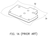
- FIG 1A illustrates a conventional electromagnetic wave shielding module.
- a one-piece electromagnetic wave shielding cover body 52 is soldered onto a circuit board 54 and that is difficult to be detached and reworked.
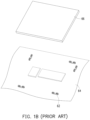
- FIG 1B illustrates another conventional electromagnetic wave shielding module.
- a clip 62 is soldered onto a circuit board 64, and an electromagnetic wave shielding cover body 66 is held by the clip 62.
- the electromagnetic wave shielding cover body 66 may be detached conveniently; nevertheless, the electromagnetic wave shielding cover body 66 and the circuit board 64 are not securely attached and thus overall structural strength is relatively insufficient.
- an overall structural thickness may increase.
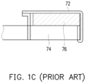
- FIG 1C illustrates another conventional electromagnetic wave shielding module.
- a conductive body 72 is coated on an integrated circuit 400 on a circuit board 74 to achieve electromagnetic wave shielding effect. Nevertheless, the electromagnetic wave shielding module is difficult to be detached and reworked since the conductive body 72 is coated on the circuit board 74.
- US2014043785 A1 discloses a shielding device and an electronic device having the same.
- the shielding device is disposed on a circuit board for covering an electronic component.
- the shielding device comprises a first case and a second case.
- the first case comprises a first limiting structure and a second limiting structure.
- the second case is mounted on the circuit board and includes a frame and a first slot.
- the frame forms an opening.
- the first slot corresponds to the first limiting structure to allow the first limiting structure to be inserted into the first slot along the first direction and the first limiting structure is prevented from moving along the second direction.
- a shield means which is suited for providing electromagnetic interference shielding for one or more electronic member/members on a substrate, generally comprises a frame (2) and a lid (1).
- the frame (2) includes sidewalls (21) which having at least one opening (22) surrounded by the upper part of this frame.
- the sidewalls (21) are defined that they can surround the one or more electronic member/members on the substrate.
- the lid (1) includes an upper surface (11) for approximately covering the at least one opening (22) of the frame (2), and elastic finger-liked members (12) downwardly extending from the upper surface (11).
- US 5436802 A discloses an electronic device which employs a method and apparatus for shielding an electrical circuit that is disposed on a substrate.
- a base member that includes a top portion and a plurality of side portions is electrically coupled to a receptacle area of the substrate such that the plurality of side portions substantially encircle the electrical circuit.
- the top portion of the base member includes a plurality of tab members interposed with a plurality of receptacle openings.
- a substantially planar cover that includes a plurality of protrusions is positioned adjacent to the top portion of the base member such that each protrusion is positioned within a corresponding receptacle opening. The cover is then urged until each protrusion interlocks with a corresponding tab member to substantially enclose and, thus, shield the electrical circuit.
- the existing electronic devices are designed to be thin and lightweight, and inevitably, internal allocation space is decreased. Therefore, how the electromagnetic wave shielding structure to be properly allocated in the limited allocation space so as to take up less space and be reworked easily becomes an important issue in electronic device design nowadays.
- the invention provides a shielding module according to the claims for saving allocation space and manufacturing costs of an electronic device and for the electronic device to be reworked easily.
- a shielding module includes a frame and a cover.
- the frame has an opening, a first plane, a plurality of side walls and a first assembling structure.
- the first plane surrounds and is adjacent to the opening. An area of the opening is larger than an area of the first plane.
- the side walls are connected to a periphery of the first plane.
- the first assembling structure is entirely formed on the first plane without extending to the side walls.
- the first assembling structure comprises at least one first engagement part and a first positioning part.
- the cover covers the opening and the first plane and has a second assembling structure. A side of the cover has a second plane parallel to the first plane.
- the second assembling structure is formed on the second plane and comprises at least one second engagement part and a second positioning part.
- the cover has no side wall.
- the second assembling structure is assembled with the first assembling structure to stop the cover from moving relative to the frame.
- the at least one engagement part and the first positioning part are both formed on the first plane.
- the at least one second engagement part and the second positioning part are both formed on the second plane.
- the at least one second engagement part is engaged with the at least one first engagement part to stop the cover from moving in a vertical direction relative to the frame.
- the second positioning part is positioned at the first positioning part to stop the cover from moving in the horizontal direction relative to the frame.
- the at least one first engagement part comprises a notch formed on the first plane.
- the at least one second engagement part includes a bent section and an engagement section. The bent section is connected between the second plane and the engagement section and is bent relative to the second plane.
- the engagement section is engaged with the at least one first engagement part through the notch.
- the at least one second engagement part further comprises an extending section connected to an end of the engagement section, the extending section is inclined relative to the second plane and has a guiding inclined surface, an extending direction of the engagement section is inclined relative to the second plane.
- the extending section and an end of the second positioning part extend from the second plane toward another side of the cover along a direction that is away from the cover.
- the engagement section is guided through the guiding inclined surface and elastically deformed, and is engaged with the first engagement part in a horizontal direction and abuts against a back surface of the frame opposite to the first plane.
- the second positioning part is positioned at the first positioning part in the vertical direction.
- the cover has at least one opening slot.
- the at least one opening slot is formed on the second plane.
- the at least one second engagement part extends from an inner edge of the at least one opening slot.
- the first positioning part includes a positioning slot formed on the first plane.
- the second positioning part includes a bent wall formed on an edge of the cover. The bent wall extends in the vertical direction.
- the first positioning part includes a guiding inclined surface
- the bent wall is adapted to move toward the positioning slot through guiding of the guiding inclined surface
- a number of the at least one first engagement part is plural.
- a gap between two adjacent ones of the first engagement parts is 2 mm to 7 mm.
- a number of the at least one second engagement part is plural.
- a gap between two adjacent ones of the second engagement parts is 2 mm to 7 mm.
- the cover has at least one extending part, and the at least one extending part is adjacent to the second positioning part and is adapted to be forced to drive the second positioning part to separate from the first positioning part.
- the frame has a plurality of side walls, and the side walls are connected to a periphery of the first plane and perpendicular to the first plane.
- the cover has no side wall.
- the shielding module includes a circuit board.
- the frame is disposed on the circuit board, and the frame and the cover mask at least one electronic element on the circuit board.
- a material of the cover and the frame is metal, and the shielding module is an electromagnetic wave shielding module.
- a structure configured to be combined with the cover is not required to be formed at the side walls by the frame, and the cover is not required to have a side wall configured to be combined with the frame either. Therefore, the height of the side walls of the frame may be reduced and the structure of the cover may be simplified to save allocation space and manufacturing costs of the electronic device. Furthermore, the end of the second assembling structure (i.e., each of the second engagement parts and the second positioning part) extends from the upper plane of the cover (i.e., the second plane) to another side of the cover to prevent the second assembling structure from protruding upward from the upper plane of the cover, and thereby, the size of the assembling structure may be further reduced in the vertical direction. In addition, the frame and the cover are assembled with each other through being engaged with each other as described above and thus may be detached and reworked easily.
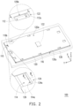
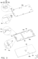
- FIG 2 is a three-dimensional view of an shielding module according to an embodiment of the invention.
- FIG 3 is an exploded view of the shielding module in FIG 2 .
- an shielding module 100 provided by the embodiment includes a frame 110 and a cover 120.
- the frame 110 is assembled with the cover 120.
- a material of the frame 110 and the cover 120 is, for example, metal, such that the shielding module 100 may act as an electromagnetic wave shielding module. But the invention is not limited thereto.
- the shielding module 100 further includes a circuit board 130.
- the frame 110 is soldered onto the circuit board 130 through, for example, the surface mounting technology (SMT) and is electrically connected to a ground plane of the circuit board 130, such that masking and shielding are performed to an electronic element 132 on the circuit board 130 through the frame 110 and the cover 120.
- SMT surface mounting technology
- the frame 110 has an opening 110a, a first plane 110b, a plurality of side walls 116, and a first assembling structure.
- the first assembling structure includes a plurality of first engagement parts 112 and a first positioning part 114.
- the first plane 110b is an outer surface of an upper side of the frame 110 and surrounds and is adjacent to the opening 110a of the frame 110.
- An area of the opening 110a is larger than an area of the first plane 110b.
- the side walls 116 are connected to a periphery of a first plane 110b and perpendicular to the first plane 110b.
- a height of each of the side walls 116 is, for example, equal to or slightly greater than a thickness of the electronic element 132, such that sufficient space is provided for the electronic element 132 to be disposed therein.
- the first assembling structure i.e., each of the first engagement parts 112 and the first positioning part 114) is formed on the first plane 110b of the frame 110.
- the cover 120 covers the opening 110a of the frame 110 and the first plane 110b and has a second assembling structure.
- the second assembling structure includes a plurality of second engagement parts 122 and a second positioning part 124.
- a side of the cover 120 has a second plane 120a parallel to the first plane 110b.
- Each of the second engagement parts 122 and the second positioning part 124 are formed on the second plane 120a of the cover 120.
- the second plane 120a is an unbent horizontal plane.
- An end of the second assembling structure i.e., each of the second engagement parts 122 and the second positioning part 124) extends from the second plane 120a to another side of the cover 120.
- the second assembling structure i.e., each of the second engagement parts 122 and the second positioning parts 124 is assembled with the first assembling structure (i.e., each of the first engagement parts 112 and the first positioning part 114) to stop the cover 120 from moving relative to the frame 110.
- each of the second engagement parts 122 is engaged with each of the first engagement parts 112 in a horizontal direction Y parallel to the first plane 110b to stop the cover 120 from moving relative to the frame 110 in a vertical direction Z perpendicular to the horizontal direction Y.
- the second positioning part 124 is positioned at the first positioning part 114 in the vertical direction Z to stop the cover 120 from moving relative to the frame 110 in the horizontal direction Y and to stop the cover 120 from moving relative to the frame 110 in a horizontal direction X.
- the electronic element 132 is disposed on a third plane 130a on the circuit board 130.
- the first plane 110b of the frame 110, the second plane 120a of the cover 120, and the third plane 130a of the circuit board 130 are parallel to each other.
- each of the first engagement parts 112 and the first positioning part 114 are both formed on an upper plane of the frame 110 (i.e., the first plane 110b), and each of the second engagement parts 122 and the second positioning part 124 are both formed on an upper plane of the cover 120 (i.e., the second plane 120a).
- the first engagement parts 112 and the first positioning part 114 are respectively matched with the second engagement parts 122 and the second positioning part 124, and that the cover 120 is fixed on the frame 110 at the upper planes.
- the frame 110 and the cover 120 are not required to be engaged with each other and be positioned at a lateral surface of the shielding module 100.
- a structure configured to be combined with the cover 120 is not required to be formed at the side walls 116 by the frame 110, and the cover 120 is not required to have a side wall configured to be combined with the frame 110. Therefore, the height of the side walls 116 of the frame 110 may be lowered and a structure of the cover 120 may be simplified to save allocation space and manufacturing costs of an electronic device.
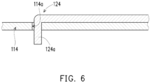
- FIG 4 is a cross-sectional view taken along a line I-I of the shielding module in FIG 2 .
- the first engagement part 112 includes a notch 112a formed on the first plane 110b as shown in FIG 2 to FIG 4 .
- the cover 120 has a plurality of opening slots 120b as shown in FIG 2 to FIG 4 .
- Each of the opening slots 120b is formed on the second plane 120a of the cover 120.
- Each of the second engagement parts 122 extends from an inner edge of the corresponding opening slots 120b.
- the second engagement part 122 includes a bent section 122a and an engagement section122b.
- the bent section 122a is connected between the second plane 120a of the cover 120 and the engagement section 122b and is bent relative to the second plane 120a, such that the engagement section 122b is engaged with the first engagement part 112 through the notch 112a.
- FIG 5 illustrates the second engagement part separates from the first engagement part in FIG 4 .
- an extending direction of the engagement section 122b is inclined relative to the second plane 120a.
- the engagement section 122b is forced and elastically deformed downward.
- an upward holding force may be generated by the engagement section 122b in FIG 4 and applied to the first engagement part 112, such that the cover 120 is securely fixed onto the frame 110.
- first engagement part 112 and the second engagement part 122 may be other structures that may be engaged with each other. The invention is not limited thereto.
- the cover 120 has two extending parts 126 as shown in FIG 2 and FIG 3 .
- the two extending parts 126 are respectively adjacent to opposite sides of the second positioning part 124 and adapted to be forced to drive the second positioning part 124 to separate from the first positioning part 114.
- the user may flip the two extending parts 126 upward.
- a portion of the cover 120 is elastically deformed and that the bent wall 124a is separated upward from the positioning slot 114a.
- the cover 120 is moved in the horizontal direction and thereby, the second engagement parts 122 are not engaged with the corresponding first engagement parts 112.
- FIG 7 is a flowchart of an assembling method of an shielding module according to an embodiment of the invention.
- the frame 110 is provided.
- the frame 110 has the opening 110a, the at least one first engagement part 112 and the first positioning part 114 (step S602).
- the cover 120 is provided.
- the cover 120 has the at least one second engagement part122 and the second positioning part 124 (step S604).
- the frame 110 is soldered onto the circuit board 130 (step S606A).
- the at least one second engagement part 122 is engaged with the at least one first engagement part 112 in the horizontal direction Y, and the second positioning part 124 is positioned at the first positioning part 114 in the vertical direction Z perpendicular to the horizontal direction Y to fix the cover 120 onto the frame 110 (step S608A).
- the frame 110 has two extending parts 118 as shown in FIG 3 .
- Each of the extending parts 118 extends from the first plane 110b into the opening 110a.
- an attraction force provided by an attraction-force-providing device may be applied to each of the extending parts 118 of the frame 110. As such, the frame 110 is moved onto the circuit board 130 for following soldering process to be performed.
- the second engagement part 122 provided by the embodiment includes an extending section 122c as shown in FIG 3 and FIG 4 .
- the extending section 122c is connected to an end of the engagement section 122b and has a guiding inclined surface S1.
- the engagement section 122b of the second engagement part 122 may be guided to be engaged with the first engagement part 112 through the inclined surface S1 of the second engagement part 122.
- the frame 110 is first soldered onto the circuit board 130 and next the cover 120 is assembled with the frame 110.
- the second engagement part 122 may first be engaged with the first engagement part 112 in the horizontal direction Y, and the second positioning part 114 is positioned at the first positioning part 114 in the vertical direction Z perpendicular to the horizontal direction Y, such that the cover 120 is fixed onto the frame 110 (step S606B).
- the frame 110 is soldered onto a circuit board 130 (step S608B). In other words, the cover 120 is first assembled with the frame 110 and then the frame 110 is soldered onto the circuit board 130.
- the frame 110 and the cover 120 are not engaged nor positioned at the side walls 116 of the frame 110 as described above. Moreover, as the cover 120 has no side wall, and thereby, during the soldering process, the side walls 116 of the frame 110 may not be in contact with a soldering material, which may lead to the cover 120 is soldered and fixed onto the frame 110 unexpectedly.
- the attraction force provided by the attraction-force-providing device may first be applied to the cover 120. As such, the cover 120 and the frame 110 are moved onto the circuit board 130 for following soldering process to be performed. Through such the assembling manner, the frame 110 may not need to have the extending parts 118 for the attraction force to be applied on.
- a structure configured to be combined with the cover is not required to be formed at the side walls by the frame, and the cover is not required to have a side wall configured to be combined with the frame either. Therefore, the height of the side walls of the frame may be reduced and the structure of the cover may be simplified to save allocation space and manufacturing costs of the electronic device. Furthermore, the end of the second assembling structure (i.e., each of the second engagement parts and the second positioning part) extends from the upper plane of the cover (i.e., the second plane) to another side of the cover to prevent the second assembling structure from protruding upward from the upper plane of the cover, and thereby, the size of the assembling structure may be further reduced in the vertical direction. In addition, the frame and the cover are assembled with each other through being engaged with each other as described above and thus may be detached and reworked easily.
Landscapes
- Engineering & Computer Science (AREA)
- Microelectronics & Electronic Packaging (AREA)
- Signal Processing (AREA)
- Shielding Devices Or Components To Electric Or Magnetic Fields (AREA)
- Casings For Electric Apparatus (AREA)
Claims (10)
- Ein Abschirmmodul (100), umfassend:einen Rahmen (110), der eine Öffnung (110a), eine erste Ebene (110b), eine Vielzahl von Seitenwänden (116) und eine erste Montagestruktur aufweist, wobei die erste Ebene (110b) die Öffnung (110a) umgibt und an diese angrenzt, eine Fläche der Öffnung (110a) größer ist als eine Fläche der ersten Ebene (110b), die Seitenwände (116) mit einer Peripherie der ersten Ebene (110b) verbunden sind, die erste Montagestruktur vollständig auf der ersten Ebene (110b) ausgebildet ist, ohne sich zu den Seitenwänden (116) zu erstrecken, und die erste Montagestruktur mindestens ein erstes Eingriffsteil (112) und ein erstes Positionierungsteil (114) umfasst; undeine Abdeckung (120), die die Öffnung (110a) und die erste Ebene (110b) abdeckt und eine zweite Montagestruktur aufweist, wobei eine Seite der Abdeckung (120) eine zweite Ebene (120a) parallel zu der ersten Ebene (110b) aufweist, die zweite Montagestruktur auf der zweiten Ebene (120a) ausgebildet ist und mindestens ein zweites Eingriffsteil (122) und ein zweites Positionierungsteil (124) umfasst, und die Abdeckung (120) keine Seitenwand aufweist,wobei die zweite Montagestruktur mit der ersten Montagestruktur zusammengebaut wird, um zu verhindern, dass sich die Abdeckung (120) relativ zu dem Rahmen (110) bewegt,das mindestens eine erste Eingriffsteil (112) und das erste Positionierungsteil (114) sind beide auf der ersten Ebene (110b) ausgebildet, das mindestens eine zweite Eingriffsteil (122) und das zweite Positionierungsteil (124) sind beide auf der zweiten Ebene (120a) ausgebildet, das zweite Eingriffsteil (122) mit dem ersten Eingriffsteil (112) in Eingriff steht, um zu verhindern, dass sich die Abdeckung (120) in einer vertikalen Richtung (Z) relativ zu dem Rahmen (110) bewegt, und das zweite Positionierungsteil (124) an dem ersten Positionierungsteil (114) positioniert ist, um zu verhindern, dass sich die Abdeckung (120) in der horizontalen Richtung (Y) relativ zu dem Rahmen (110) bewegt,das mindestens eine erste Eingriffsteil (112) eine Kerbe (112a) aufweist, die auf der ersten Ebene (110b) ausgebildet ist, das mindestens eine zweite Eingriffsteil (122) einen gebogenen Abschnitt (122a) und einen Eingriffsabschnitt (122b) aufweist, der gebogene Abschnitt (122a) zwischen der zweiten Ebene (120a) und dem Eingriffsabschnitt (122b) verbunden ist und relativ zu der zweiten Ebene (120a) gebogen ist, und der Eingriffsabschnitt (122b) mit dem mindestens einen ersten Eingriffsteil (112) durch die Kerbe (112a) in Eingriff istwobei das mindestens eine zweite Eingriffsteil (122) ferner einen Verlängerungsabschnitt (122c) umfasst, der mit einem Ende des Eingriffsabschnitts (122b) verbunden ist, wobei der Verlängerungsabschnitt (122c) relativ zu der zweiten Ebene (120a) geneigt ist und eine geneigte Führungsfläche (S1) aufweist, wobei eine Erstreckungsrichtung des Eingriffsabschnitts (122b) relativ zu der zweiten Ebene (120a) geneigt ist, der Erstreckungsabschnitt (122c) und ein Ende des zweiten Positionierungsteils (124) sich beide zu einer anderen Seite der Abdeckung (120) von der zweiten Ebene (120a) entlang einer Richtung erstrecken, die von der Abdeckung (120) weg ist, der Eingriffsabschnitt (122b) durch die geneigte Führungsfläche (S1) geführt und elastisch verformt wird und mit dem ersten Eingriffsteil (112) in einer horizontalen Richtung (Y) in Eingriff steht und gegen eine hintere Fläche des Rahmens (110) gegenüber der ersten Ebene (110a) stößt,wobei das erste Positionierungsteil (114) einen Positionierungsschlitz (114a) umfasst, der auf der ersten Ebene (110b) ausgebildet ist, das zweite Positionierungsteil (124) eine gebogene Wand (124a) umfasst, die an einer Kante der Abdeckung (120) ausgebildet ist, und die gebogene Wand (124a) sich in der vertikalen Richtung (Z) erstreckt,wobei das erste Positionierungsteil (114) eine geneigte Führungsfläche (S2) umfasst und die gebogene Wand (124a) so angepasst ist, dass sie sich durch die Führung der geneigten Führungsfläche (S2) in Richtung des Positionierungsschlitzes (114a) bewegt.
- Das Abschirmmodul (100) nach Anspruch 1, wobei das zweite Positionierungsteil (124) in vertikaler Richtung (Z) an dem ersten Positionierungsteil (114) positioniert ist.
- Das Abschirmmodul (100) nach Anspruch 2, wobei die Abdeckung (120) mindestens einen Öffnungsschlitz (120b) aufweist, der mindestens eine Öffnungsschlitz (120b) vollständig auf der zweiten Ebene (120a) ausgebildet ist und sich das mindestens eine zweite Eingriffsteil (122) von einer Innenkante des mindestens einen Öffnungsschlitzes (120b) erstreckt.
- Das Abschirmmodul (100) nach einem der Ansprüche 1 bis 3, wobei eine Anzahl des mindestens einen ersten Eingriffsteils (112) mehrere ist, ein Abstand zwischen zwei benachbarten der ersten Eingriffsteile (112) 2 mm bis 7 mm beträgt, eine Anzahl des mindestens einen zweiten Eingriffsteils (122) mehrere ist und ein Abstand zwischen zwei benachbarten der zweiten Eingriffsteile (122) 2 mm bis 7 mm beträgt.
- Das Abschirmmodul (100) nach einem der Ansprüche 1 bis 4, wobei die Abdeckung (120) mindestens ein ausfahrendes Teil (126) aufweist, und das mindestens eine ausfahrende Teil (126) an das zweite Positionierungsteil (124) angrenzt und so ausgebildet ist, dass es gezwungen wird, das zweite Positionierungsteil (124) vom ersten Positionierungsteil (114) zu trennen.
- Das Abschirmmodul (100) nach einem der Ansprüche 1 bis 5, wobei der Rahmen (110) mindestens ein ausfahrendes Teil (118) aufweist, wobei sich das mindestens eine ausfahrende Teil (118) von der ersten Ebene (110b) in die Öffnung (110a) hinein erstreckt, und wobei eine Anziehungskraft auf das mindestens eine ausfahrende Teil (118) ausgeübt werden kann, um den Rahmen (110) zu bewegen.
- Das Abschirmmodul (100) nach einem der Ansprüche 1 bis 6, wobei die Seitenwände (116) senkrecht zur ersten Ebene (110b) verlaufen.
- Das Abschirmmodul (100) nach einem der Ansprüche 1 bis 7, umfassend eine Leiterplatte (130), wobei der Rahmen (110) auf der Leiterplatte (130) angeordnet ist und der Rahmen (110) und die Abdeckung (120) mindestens ein elektronisches Element (132) auf der Leiterplatte (130) abdecken.
- Das Abschirmmodul (100) nach Anspruch 7, wobei das mindestens eine elektronische Element (132) auf einer dritten Ebene (130a) auf der Leiterplatte (130) angeordnet ist und die erste Ebene (110b) und die zweite Ebene (120a) parallel zu der dritten Ebene (130a) verlaufen.
- Das Abschirmmodul (100) nach einem der Ansprüche 1 bis 9, wobei ein Material der Abdeckung (120) und des Rahmens (110) Metall ist und das Abschirmmodul (100) ein Modul zur Abschirmung elektromagnetischer Wellen ist.
Applications Claiming Priority (1)
| Application Number | Priority Date | Filing Date | Title |
|---|---|---|---|
| TW106106349A TWI682707B (zh) | 2017-02-24 | 2017-02-24 | 組裝組件及其組裝方法 |
Publications (3)
| Publication Number | Publication Date |
|---|---|
| EP3367772A1 EP3367772A1 (de) | 2018-08-29 |
| EP3367772B1 true EP3367772B1 (de) | 2025-05-28 |
| EP3367772C0 EP3367772C0 (de) | 2025-05-28 |
Family
ID=59699471
Family Applications (1)
| Application Number | Title | Priority Date | Filing Date |
|---|---|---|---|
| EP17185233.8A Active EP3367772B1 (de) | 2017-02-24 | 2017-08-08 | Montagekomponente |
Country Status (4)
| Country | Link |
|---|---|
| US (1) | US10257968B2 (de) |
| EP (1) | EP3367772B1 (de) |
| CN (1) | CN108513522B (de) |
| TW (1) | TWI682707B (de) |
Families Citing this family (2)
| Publication number | Priority date | Publication date | Assignee | Title |
|---|---|---|---|---|
| CN110830625B (zh) * | 2019-11-14 | 2021-03-26 | 华勤技术股份有限公司 | 壳体及包含其的移动终端 |
| CN112423469A (zh) * | 2021-01-04 | 2021-02-26 | 四川赛狄信息技术股份公司 | 一种电路板双芯片居中抗震加强结构及控制器电路板 |
Citations (2)
| Publication number | Priority date | Publication date | Assignee | Title |
|---|---|---|---|---|
| US5436802A (en) * | 1994-03-16 | 1995-07-25 | Motorola | Method and apparatus for shielding an electrical circuit that is disposed on a substrate |
| US20060121784A1 (en) * | 2004-12-04 | 2006-06-08 | Hon Hai Precision Industry Co., Ltd. | Electromagnetic interference shield |
Family Cites Families (21)
| Publication number | Priority date | Publication date | Assignee | Title |
|---|---|---|---|---|
| JP2501638Y2 (ja) * | 1991-11-25 | 1996-06-19 | 船井電機株式会社 | プリント基板装着用シ―ルド板 |
| DE19636182A1 (de) * | 1996-09-06 | 1998-03-12 | Philips Patentverwaltung | Abschirmgehäuse für elektronische Bauelemente |
| US6140577A (en) * | 1998-10-08 | 2000-10-31 | Gateway 2000, Inc | Electronic chassis electro-magnetic interference seal and sealing device |
| US6274808B1 (en) * | 1999-05-06 | 2001-08-14 | Lucent Technologies, Inc. | EMI shielding enclosure |
| CN101340806B (zh) * | 2007-07-06 | 2012-10-31 | 莱尔德电子材料(上海)有限公司 | 屏蔽装置和制造屏蔽装置的方法 |
| CN101472453B (zh) * | 2007-12-29 | 2012-01-18 | 鸿富锦精密工业(深圳)有限公司 | 电磁屏蔽装置 |
| JP2012530758A (ja) * | 2009-06-24 | 2012-12-06 | ベーリンガー インゲルハイム インターナショナル ゲゼルシャフト ミット ベシュレンクテル ハフツング | 新規化合物、医薬組成物及びそれに関する方法 |
| CN102036540A (zh) | 2009-09-30 | 2011-04-27 | 莱尔德技术股份有限公司 | 屏蔽外壳 |
| TWM380706U (en) * | 2009-12-10 | 2010-05-11 | Wistron Corp | Metal shielding casing and the combination thereof with circuit board |
| CN201657596U (zh) * | 2010-02-03 | 2010-11-24 | 鸿富锦精密工业(深圳)有限公司 | 电磁屏蔽装置 |
| KR101068550B1 (ko) * | 2010-02-03 | 2011-09-30 | 조인셋 주식회사 | 솔더링이 용이한 전자파 차폐용 실드 케이스 |
| CN201657591U (zh) * | 2010-03-08 | 2010-11-24 | 国基电子(上海)有限公司 | 电磁屏蔽装置 |
| GB2511682A (en) * | 2010-09-07 | 2014-09-10 | Caged Idea S Llc | Data transmission blocking holder |
| CN102548371B (zh) * | 2010-12-15 | 2015-02-04 | 和硕联合科技股份有限公司 | 电磁屏蔽模块 |
| KR101062484B1 (ko) * | 2011-05-26 | 2011-09-05 | 주식회사 성덕전자 | 전자파 차폐용 실드 |
| US20130250540A1 (en) * | 2012-03-21 | 2013-09-26 | Chih-Yuan Hou | Shielding shell |
| TWI548338B (zh) * | 2012-08-07 | 2016-09-01 | 緯創資通股份有限公司 | 屏蔽裝置及具有屏蔽裝置之電子裝置 |
| TW201410132A (zh) * | 2012-08-16 | 2014-03-01 | Wistron Corp | 電磁屏蔽組件 |
| US9462732B2 (en) * | 2013-03-13 | 2016-10-04 | Laird Technologies, Inc. | Electromagnetic interference shielding (EMI) apparatus including a frame with drawn latching features |
| CN105451528A (zh) * | 2014-08-18 | 2016-03-30 | 国基电子(上海)有限公司 | 屏蔽装置 |
| CN205847842U (zh) * | 2016-06-03 | 2016-12-28 | 上海与德通讯技术有限公司 | 主板屏蔽结构及带有主板屏蔽结构的移动终端 |
-
2017
- 2017-02-24 TW TW106106349A patent/TWI682707B/zh active
- 2017-03-16 CN CN201710158071.8A patent/CN108513522B/zh active Active
- 2017-06-02 US US15/611,794 patent/US10257968B2/en active Active
- 2017-08-08 EP EP17185233.8A patent/EP3367772B1/de active Active
Patent Citations (2)
| Publication number | Priority date | Publication date | Assignee | Title |
|---|---|---|---|---|
| US5436802A (en) * | 1994-03-16 | 1995-07-25 | Motorola | Method and apparatus for shielding an electrical circuit that is disposed on a substrate |
| US20060121784A1 (en) * | 2004-12-04 | 2006-06-08 | Hon Hai Precision Industry Co., Ltd. | Electromagnetic interference shield |
Also Published As
| Publication number | Publication date |
|---|---|
| US20180249598A1 (en) | 2018-08-30 |
| TWI682707B (zh) | 2020-01-11 |
| EP3367772C0 (de) | 2025-05-28 |
| CN108513522B (zh) | 2020-04-28 |
| TW201832640A (zh) | 2018-09-01 |
| EP3367772A1 (de) | 2018-08-29 |
| CN108513522A (zh) | 2018-09-07 |
| US10257968B2 (en) | 2019-04-09 |
Similar Documents
| Publication | Publication Date | Title |
|---|---|---|
| US6949706B2 (en) | Radio frequency shield for electronic equipment | |
| US6943287B2 (en) | Shielding cage with improved EMI shielding gasket construction | |
| US9247682B2 (en) | Electronic circuit module | |
| EP1930995A2 (de) | Elektrischer Steckverbinder | |
| US8558121B2 (en) | Electronic device having an electromagnetic shield | |
| JP4348725B2 (ja) | 電子部品取付用ソケット | |
| US6985366B2 (en) | EMC shield and housing for electronic components | |
| US8520405B2 (en) | Shield case and image display device | |
| US20090268420A1 (en) | Shielding assembly | |
| US8462519B2 (en) | Method of shielding a circuit board, circuit board, electromagnetic shield and method of manufacturing same | |
| EP3367772B1 (de) | Montagekomponente | |
| JP2006165201A (ja) | 回路モジュール装置 | |
| KR101454485B1 (ko) | 휴대 단말기의 쉴드캔 | |
| JP5224407B2 (ja) | シールドケースおよび電子機器 | |
| CN101742895B (zh) | 电子装置的屏蔽构造 | |
| JP4182529B2 (ja) | 電子部品取付用ソケット及びそれに使用するコンタクトキャリヤ | |
| CN216852796U (zh) | 走线结构及电子设备 | |
| JPH1126973A (ja) | 電子機器 | |
| KR20220138821A (ko) | 기판 커넥터 | |
| JP2003163485A (ja) | サブラックシールド構造 | |
| JP2014086479A (ja) | 電子機器 | |
| JP2005294436A (ja) | 電子機器のシールド構造 |
Legal Events
| Date | Code | Title | Description |
|---|---|---|---|
| PUAI | Public reference made under article 153(3) epc to a published international application that has entered the european phase |
Free format text: ORIGINAL CODE: 0009012 |
|
| STAA | Information on the status of an ep patent application or granted ep patent |
Free format text: STATUS: REQUEST FOR EXAMINATION WAS MADE |
|
| 17P | Request for examination filed |
Effective date: 20170808 |
|
| AK | Designated contracting states |
Kind code of ref document: A1 Designated state(s): AL AT BE BG CH CY CZ DE DK EE ES FI FR GB GR HR HU IE IS IT LI LT LU LV MC MK MT NL NO PL PT RO RS SE SI SK SM TR |
|
| AX | Request for extension of the european patent |
Extension state: BA ME |
|
| STAA | Information on the status of an ep patent application or granted ep patent |
Free format text: STATUS: EXAMINATION IS IN PROGRESS |
|
| 17Q | First examination report despatched |
Effective date: 20191023 |
|
| GRAP | Despatch of communication of intention to grant a patent |
Free format text: ORIGINAL CODE: EPIDOSNIGR1 |
|
| STAA | Information on the status of an ep patent application or granted ep patent |
Free format text: STATUS: GRANT OF PATENT IS INTENDED |
|
| INTG | Intention to grant announced |
Effective date: 20250219 |
|
| GRAS | Grant fee paid |
Free format text: ORIGINAL CODE: EPIDOSNIGR3 |
|
| GRAA | (expected) grant |
Free format text: ORIGINAL CODE: 0009210 |
|
| STAA | Information on the status of an ep patent application or granted ep patent |
Free format text: STATUS: THE PATENT HAS BEEN GRANTED |
|
| AK | Designated contracting states |
Kind code of ref document: B1 Designated state(s): AL AT BE BG CH CY CZ DE DK EE ES FI FR GB GR HR HU IE IS IT LI LT LU LV MC MK MT NL NO PL PT RO RS SE SI SK SM TR |
|
| REG | Reference to a national code |
Ref country code: GB Ref legal event code: FG4D |
|
| REG | Reference to a national code |
Ref country code: CH Ref legal event code: EP |
|
| REG | Reference to a national code |
Ref country code: IE Ref legal event code: FG4D Ref country code: DE Ref legal event code: R096 Ref document number: 602017089652 Country of ref document: DE |
|
| U01 | Request for unitary effect filed |
Effective date: 20250528 |
|
| U07 | Unitary effect registered |
Designated state(s): AT BE BG DE DK EE FI FR IT LT LU LV MT NL PT RO SE SI Effective date: 20250605 |
|
| U20 | Renewal fee for the european patent with unitary effect paid |
Year of fee payment: 9 Effective date: 20250825 |
|
| PG25 | Lapsed in a contracting state [announced via postgrant information from national office to epo] |
Ref country code: ES Free format text: LAPSE BECAUSE OF FAILURE TO SUBMIT A TRANSLATION OF THE DESCRIPTION OR TO PAY THE FEE WITHIN THE PRESCRIBED TIME-LIMIT Effective date: 20250528 |
|
| PG25 | Lapsed in a contracting state [announced via postgrant information from national office to epo] |
Ref country code: GR Free format text: LAPSE BECAUSE OF FAILURE TO SUBMIT A TRANSLATION OF THE DESCRIPTION OR TO PAY THE FEE WITHIN THE PRESCRIBED TIME-LIMIT Effective date: 20250829 Ref country code: NO Free format text: LAPSE BECAUSE OF FAILURE TO SUBMIT A TRANSLATION OF THE DESCRIPTION OR TO PAY THE FEE WITHIN THE PRESCRIBED TIME-LIMIT Effective date: 20250828 |
|
| PG25 | Lapsed in a contracting state [announced via postgrant information from national office to epo] |
Ref country code: PL Free format text: LAPSE BECAUSE OF FAILURE TO SUBMIT A TRANSLATION OF THE DESCRIPTION OR TO PAY THE FEE WITHIN THE PRESCRIBED TIME-LIMIT Effective date: 20250528 |
|
| PG25 | Lapsed in a contracting state [announced via postgrant information from national office to epo] |
Ref country code: HR Free format text: LAPSE BECAUSE OF FAILURE TO SUBMIT A TRANSLATION OF THE DESCRIPTION OR TO PAY THE FEE WITHIN THE PRESCRIBED TIME-LIMIT Effective date: 20250528 |
|
| PG25 | Lapsed in a contracting state [announced via postgrant information from national office to epo] |
Ref country code: RS Free format text: LAPSE BECAUSE OF FAILURE TO SUBMIT A TRANSLATION OF THE DESCRIPTION OR TO PAY THE FEE WITHIN THE PRESCRIBED TIME-LIMIT Effective date: 20250828 |
|
| PG25 | Lapsed in a contracting state [announced via postgrant information from national office to epo] |
Ref country code: IS Free format text: LAPSE BECAUSE OF FAILURE TO SUBMIT A TRANSLATION OF THE DESCRIPTION OR TO PAY THE FEE WITHIN THE PRESCRIBED TIME-LIMIT Effective date: 20250928 |