EP3367772B1 - Assembling component - Google Patents
Assembling component Download PDFInfo
- Publication number
- EP3367772B1 EP3367772B1 EP17185233.8A EP17185233A EP3367772B1 EP 3367772 B1 EP3367772 B1 EP 3367772B1 EP 17185233 A EP17185233 A EP 17185233A EP 3367772 B1 EP3367772 B1 EP 3367772B1
- Authority
- EP
- European Patent Office
- Prior art keywords
- plane
- cover
- engagement
- frame
- positioning part
- Prior art date
- Legal status (The legal status is an assumption and is not a legal conclusion. Google has not performed a legal analysis and makes no representation as to the accuracy of the status listed.)
- Active
Links
Images


Classifications
-
- H—ELECTRICITY
- H05—ELECTRIC TECHNIQUES NOT OTHERWISE PROVIDED FOR
- H05K—PRINTED CIRCUITS; CASINGS OR CONSTRUCTIONAL DETAILS OF ELECTRIC APPARATUS; MANUFACTURE OF ASSEMBLAGES OF ELECTRICAL COMPONENTS
- H05K9/00—Screening of apparatus or components against electric or magnetic fields
- H05K9/0007—Casings
- H05K9/006—Casings specially adapted for signal processing applications, e.g. CATV, tuner, antennas amplifier
-
- H—ELECTRICITY
- H05—ELECTRIC TECHNIQUES NOT OTHERWISE PROVIDED FOR
- H05K—PRINTED CIRCUITS; CASINGS OR CONSTRUCTIONAL DETAILS OF ELECTRIC APPARATUS; MANUFACTURE OF ASSEMBLAGES OF ELECTRICAL COMPONENTS
- H05K9/00—Screening of apparatus or components against electric or magnetic fields
- H05K9/0007—Casings
- H05K9/002—Casings with localised screening
- H05K9/0022—Casings with localised screening of components mounted on printed circuit boards [PCB]
- H05K9/0024—Shield cases mounted on a PCB, e.g. cans or caps or conformal shields
- H05K9/0032—Shield cases mounted on a PCB, e.g. cans or caps or conformal shields having multiple parts, e.g. frames mating with lids
-
- H—ELECTRICITY
- H05—ELECTRIC TECHNIQUES NOT OTHERWISE PROVIDED FOR
- H05K—PRINTED CIRCUITS; CASINGS OR CONSTRUCTIONAL DETAILS OF ELECTRIC APPARATUS; MANUFACTURE OF ASSEMBLAGES OF ELECTRICAL COMPONENTS
- H05K9/00—Screening of apparatus or components against electric or magnetic fields
- H05K9/0073—Shielding materials
- H05K9/0075—Magnetic shielding materials
-
- H—ELECTRICITY
- H05—ELECTRIC TECHNIQUES NOT OTHERWISE PROVIDED FOR
- H05K—PRINTED CIRCUITS; CASINGS OR CONSTRUCTIONAL DETAILS OF ELECTRIC APPARATUS; MANUFACTURE OF ASSEMBLAGES OF ELECTRICAL COMPONENTS
- H05K9/00—Screening of apparatus or components against electric or magnetic fields
- H05K9/0067—Devices for protecting against damage from electrostatic discharge
Definitions
- the invention relates to a shielding module. More particularly, the invention relates to an assembling component.
- electromagnetic waves are generated most of the time, and signal quality and working performance of other electronic elements are thus affected.
- the electromagnetic waves generated by the electronic element may become noise which causes interference to an antenna in the electronic device, and capabilities of sending and receiving signals of the antenna are thereby lowered. This is called electromagnetic interference (EMI).
- EMI electromagnetic interference
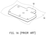
- FIG 1A illustrates a conventional electromagnetic wave shielding module.
- a one-piece electromagnetic wave shielding cover body 52 is soldered onto a circuit board 54 and that is difficult to be detached and reworked.
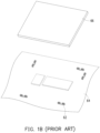
- FIG 1B illustrates another conventional electromagnetic wave shielding module.
- a clip 62 is soldered onto a circuit board 64, and an electromagnetic wave shielding cover body 66 is held by the clip 62.
- the electromagnetic wave shielding cover body 66 may be detached conveniently; nevertheless, the electromagnetic wave shielding cover body 66 and the circuit board 64 are not securely attached and thus overall structural strength is relatively insufficient.
- an overall structural thickness may increase.
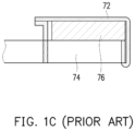
- FIG 1C illustrates another conventional electromagnetic wave shielding module.
- a conductive body 72 is coated on an integrated circuit 400 on a circuit board 74 to achieve electromagnetic wave shielding effect. Nevertheless, the electromagnetic wave shielding module is difficult to be detached and reworked since the conductive body 72 is coated on the circuit board 74.
- US2014043785 A1 discloses a shielding device and an electronic device having the same.
- the shielding device is disposed on a circuit board for covering an electronic component.
- the shielding device comprises a first case and a second case.
- the first case comprises a first limiting structure and a second limiting structure.
- the second case is mounted on the circuit board and includes a frame and a first slot.
- the frame forms an opening.
- the first slot corresponds to the first limiting structure to allow the first limiting structure to be inserted into the first slot along the first direction and the first limiting structure is prevented from moving along the second direction.
- a shield means which is suited for providing electromagnetic interference shielding for one or more electronic member/members on a substrate, generally comprises a frame (2) and a lid (1).
- the frame (2) includes sidewalls (21) which having at least one opening (22) surrounded by the upper part of this frame.
- the sidewalls (21) are defined that they can surround the one or more electronic member/members on the substrate.
- the lid (1) includes an upper surface (11) for approximately covering the at least one opening (22) of the frame (2), and elastic finger-liked members (12) downwardly extending from the upper surface (11).
- US 5436802 A discloses an electronic device which employs a method and apparatus for shielding an electrical circuit that is disposed on a substrate.
- a base member that includes a top portion and a plurality of side portions is electrically coupled to a receptacle area of the substrate such that the plurality of side portions substantially encircle the electrical circuit.
- the top portion of the base member includes a plurality of tab members interposed with a plurality of receptacle openings.
- a substantially planar cover that includes a plurality of protrusions is positioned adjacent to the top portion of the base member such that each protrusion is positioned within a corresponding receptacle opening. The cover is then urged until each protrusion interlocks with a corresponding tab member to substantially enclose and, thus, shield the electrical circuit.
- the existing electronic devices are designed to be thin and lightweight, and inevitably, internal allocation space is decreased. Therefore, how the electromagnetic wave shielding structure to be properly allocated in the limited allocation space so as to take up less space and be reworked easily becomes an important issue in electronic device design nowadays.
- the invention provides a shielding module according to the claims for saving allocation space and manufacturing costs of an electronic device and for the electronic device to be reworked easily.
- a shielding module includes a frame and a cover.
- the frame has an opening, a first plane, a plurality of side walls and a first assembling structure.
- the first plane surrounds and is adjacent to the opening. An area of the opening is larger than an area of the first plane.
- the side walls are connected to a periphery of the first plane.
- the first assembling structure is entirely formed on the first plane without extending to the side walls.
- the first assembling structure comprises at least one first engagement part and a first positioning part.
- the cover covers the opening and the first plane and has a second assembling structure. A side of the cover has a second plane parallel to the first plane.
- the second assembling structure is formed on the second plane and comprises at least one second engagement part and a second positioning part.
- the cover has no side wall.
- the second assembling structure is assembled with the first assembling structure to stop the cover from moving relative to the frame.
- the at least one engagement part and the first positioning part are both formed on the first plane.
- the at least one second engagement part and the second positioning part are both formed on the second plane.
- the at least one second engagement part is engaged with the at least one first engagement part to stop the cover from moving in a vertical direction relative to the frame.
- the second positioning part is positioned at the first positioning part to stop the cover from moving in the horizontal direction relative to the frame.
- the at least one first engagement part comprises a notch formed on the first plane.
- the at least one second engagement part includes a bent section and an engagement section. The bent section is connected between the second plane and the engagement section and is bent relative to the second plane.
- the engagement section is engaged with the at least one first engagement part through the notch.
- the at least one second engagement part further comprises an extending section connected to an end of the engagement section, the extending section is inclined relative to the second plane and has a guiding inclined surface, an extending direction of the engagement section is inclined relative to the second plane.
- the extending section and an end of the second positioning part extend from the second plane toward another side of the cover along a direction that is away from the cover.
- the engagement section is guided through the guiding inclined surface and elastically deformed, and is engaged with the first engagement part in a horizontal direction and abuts against a back surface of the frame opposite to the first plane.
- the second positioning part is positioned at the first positioning part in the vertical direction.
- the cover has at least one opening slot.
- the at least one opening slot is formed on the second plane.
- the at least one second engagement part extends from an inner edge of the at least one opening slot.
- the first positioning part includes a positioning slot formed on the first plane.
- the second positioning part includes a bent wall formed on an edge of the cover. The bent wall extends in the vertical direction.
- the first positioning part includes a guiding inclined surface
- the bent wall is adapted to move toward the positioning slot through guiding of the guiding inclined surface
- a number of the at least one first engagement part is plural.
- a gap between two adjacent ones of the first engagement parts is 2 mm to 7 mm.
- a number of the at least one second engagement part is plural.
- a gap between two adjacent ones of the second engagement parts is 2 mm to 7 mm.
- the cover has at least one extending part, and the at least one extending part is adjacent to the second positioning part and is adapted to be forced to drive the second positioning part to separate from the first positioning part.
- the frame has a plurality of side walls, and the side walls are connected to a periphery of the first plane and perpendicular to the first plane.
- the cover has no side wall.
- the shielding module includes a circuit board.
- the frame is disposed on the circuit board, and the frame and the cover mask at least one electronic element on the circuit board.
- a material of the cover and the frame is metal, and the shielding module is an electromagnetic wave shielding module.
- a structure configured to be combined with the cover is not required to be formed at the side walls by the frame, and the cover is not required to have a side wall configured to be combined with the frame either. Therefore, the height of the side walls of the frame may be reduced and the structure of the cover may be simplified to save allocation space and manufacturing costs of the electronic device. Furthermore, the end of the second assembling structure (i.e., each of the second engagement parts and the second positioning part) extends from the upper plane of the cover (i.e., the second plane) to another side of the cover to prevent the second assembling structure from protruding upward from the upper plane of the cover, and thereby, the size of the assembling structure may be further reduced in the vertical direction. In addition, the frame and the cover are assembled with each other through being engaged with each other as described above and thus may be detached and reworked easily.
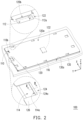
- FIG 2 is a three-dimensional view of an shielding module according to an embodiment of the invention.
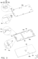
- FIG 3 is an exploded view of the shielding module in FIG 2 .
- an shielding module 100 provided by the embodiment includes a frame 110 and a cover 120.
- the frame 110 is assembled with the cover 120.
- a material of the frame 110 and the cover 120 is, for example, metal, such that the shielding module 100 may act as an electromagnetic wave shielding module. But the invention is not limited thereto.
- the shielding module 100 further includes a circuit board 130.
- the frame 110 is soldered onto the circuit board 130 through, for example, the surface mounting technology (SMT) and is electrically connected to a ground plane of the circuit board 130, such that masking and shielding are performed to an electronic element 132 on the circuit board 130 through the frame 110 and the cover 120.
- SMT surface mounting technology
- the frame 110 has an opening 110a, a first plane 110b, a plurality of side walls 116, and a first assembling structure.
- the first assembling structure includes a plurality of first engagement parts 112 and a first positioning part 114.
- the first plane 110b is an outer surface of an upper side of the frame 110 and surrounds and is adjacent to the opening 110a of the frame 110.
- An area of the opening 110a is larger than an area of the first plane 110b.
- the side walls 116 are connected to a periphery of a first plane 110b and perpendicular to the first plane 110b.
- a height of each of the side walls 116 is, for example, equal to or slightly greater than a thickness of the electronic element 132, such that sufficient space is provided for the electronic element 132 to be disposed therein.
- the first assembling structure i.e., each of the first engagement parts 112 and the first positioning part 114) is formed on the first plane 110b of the frame 110.
- the cover 120 covers the opening 110a of the frame 110 and the first plane 110b and has a second assembling structure.
- the second assembling structure includes a plurality of second engagement parts 122 and a second positioning part 124.
- a side of the cover 120 has a second plane 120a parallel to the first plane 110b.
- Each of the second engagement parts 122 and the second positioning part 124 are formed on the second plane 120a of the cover 120.
- the second plane 120a is an unbent horizontal plane.
- An end of the second assembling structure i.e., each of the second engagement parts 122 and the second positioning part 124) extends from the second plane 120a to another side of the cover 120.
- the second assembling structure i.e., each of the second engagement parts 122 and the second positioning parts 124 is assembled with the first assembling structure (i.e., each of the first engagement parts 112 and the first positioning part 114) to stop the cover 120 from moving relative to the frame 110.
- each of the second engagement parts 122 is engaged with each of the first engagement parts 112 in a horizontal direction Y parallel to the first plane 110b to stop the cover 120 from moving relative to the frame 110 in a vertical direction Z perpendicular to the horizontal direction Y.
- the second positioning part 124 is positioned at the first positioning part 114 in the vertical direction Z to stop the cover 120 from moving relative to the frame 110 in the horizontal direction Y and to stop the cover 120 from moving relative to the frame 110 in a horizontal direction X.
- the electronic element 132 is disposed on a third plane 130a on the circuit board 130.
- the first plane 110b of the frame 110, the second plane 120a of the cover 120, and the third plane 130a of the circuit board 130 are parallel to each other.
- each of the first engagement parts 112 and the first positioning part 114 are both formed on an upper plane of the frame 110 (i.e., the first plane 110b), and each of the second engagement parts 122 and the second positioning part 124 are both formed on an upper plane of the cover 120 (i.e., the second plane 120a).
- the first engagement parts 112 and the first positioning part 114 are respectively matched with the second engagement parts 122 and the second positioning part 124, and that the cover 120 is fixed on the frame 110 at the upper planes.
- the frame 110 and the cover 120 are not required to be engaged with each other and be positioned at a lateral surface of the shielding module 100.
- a structure configured to be combined with the cover 120 is not required to be formed at the side walls 116 by the frame 110, and the cover 120 is not required to have a side wall configured to be combined with the frame 110. Therefore, the height of the side walls 116 of the frame 110 may be lowered and a structure of the cover 120 may be simplified to save allocation space and manufacturing costs of an electronic device.
- FIG 4 is a cross-sectional view taken along a line I-I of the shielding module in FIG 2 .
- the first engagement part 112 includes a notch 112a formed on the first plane 110b as shown in FIG 2 to FIG 4 .
- the cover 120 has a plurality of opening slots 120b as shown in FIG 2 to FIG 4 .
- Each of the opening slots 120b is formed on the second plane 120a of the cover 120.
- Each of the second engagement parts 122 extends from an inner edge of the corresponding opening slots 120b.
- the second engagement part 122 includes a bent section 122a and an engagement section122b.
- the bent section 122a is connected between the second plane 120a of the cover 120 and the engagement section 122b and is bent relative to the second plane 120a, such that the engagement section 122b is engaged with the first engagement part 112 through the notch 112a.
- FIG 5 illustrates the second engagement part separates from the first engagement part in FIG 4 .
- an extending direction of the engagement section 122b is inclined relative to the second plane 120a.
- the engagement section 122b is forced and elastically deformed downward.
- an upward holding force may be generated by the engagement section 122b in FIG 4 and applied to the first engagement part 112, such that the cover 120 is securely fixed onto the frame 110.
- first engagement part 112 and the second engagement part 122 may be other structures that may be engaged with each other. The invention is not limited thereto.
- the cover 120 has two extending parts 126 as shown in FIG 2 and FIG 3 .
- the two extending parts 126 are respectively adjacent to opposite sides of the second positioning part 124 and adapted to be forced to drive the second positioning part 124 to separate from the first positioning part 114.
- the user may flip the two extending parts 126 upward.
- a portion of the cover 120 is elastically deformed and that the bent wall 124a is separated upward from the positioning slot 114a.
- the cover 120 is moved in the horizontal direction and thereby, the second engagement parts 122 are not engaged with the corresponding first engagement parts 112.
- FIG 7 is a flowchart of an assembling method of an shielding module according to an embodiment of the invention.
- the frame 110 is provided.
- the frame 110 has the opening 110a, the at least one first engagement part 112 and the first positioning part 114 (step S602).
- the cover 120 is provided.
- the cover 120 has the at least one second engagement part122 and the second positioning part 124 (step S604).
- the frame 110 is soldered onto the circuit board 130 (step S606A).
- the at least one second engagement part 122 is engaged with the at least one first engagement part 112 in the horizontal direction Y, and the second positioning part 124 is positioned at the first positioning part 114 in the vertical direction Z perpendicular to the horizontal direction Y to fix the cover 120 onto the frame 110 (step S608A).
- the frame 110 has two extending parts 118 as shown in FIG 3 .
- Each of the extending parts 118 extends from the first plane 110b into the opening 110a.
- an attraction force provided by an attraction-force-providing device may be applied to each of the extending parts 118 of the frame 110. As such, the frame 110 is moved onto the circuit board 130 for following soldering process to be performed.
- the second engagement part 122 provided by the embodiment includes an extending section 122c as shown in FIG 3 and FIG 4 .
- the extending section 122c is connected to an end of the engagement section 122b and has a guiding inclined surface S1.
- the engagement section 122b of the second engagement part 122 may be guided to be engaged with the first engagement part 112 through the inclined surface S1 of the second engagement part 122.
- the frame 110 is first soldered onto the circuit board 130 and next the cover 120 is assembled with the frame 110.
- the second engagement part 122 may first be engaged with the first engagement part 112 in the horizontal direction Y, and the second positioning part 114 is positioned at the first positioning part 114 in the vertical direction Z perpendicular to the horizontal direction Y, such that the cover 120 is fixed onto the frame 110 (step S606B).
- the frame 110 is soldered onto a circuit board 130 (step S608B). In other words, the cover 120 is first assembled with the frame 110 and then the frame 110 is soldered onto the circuit board 130.
- the frame 110 and the cover 120 are not engaged nor positioned at the side walls 116 of the frame 110 as described above. Moreover, as the cover 120 has no side wall, and thereby, during the soldering process, the side walls 116 of the frame 110 may not be in contact with a soldering material, which may lead to the cover 120 is soldered and fixed onto the frame 110 unexpectedly.
- the attraction force provided by the attraction-force-providing device may first be applied to the cover 120. As such, the cover 120 and the frame 110 are moved onto the circuit board 130 for following soldering process to be performed. Through such the assembling manner, the frame 110 may not need to have the extending parts 118 for the attraction force to be applied on.
- a structure configured to be combined with the cover is not required to be formed at the side walls by the frame, and the cover is not required to have a side wall configured to be combined with the frame either. Therefore, the height of the side walls of the frame may be reduced and the structure of the cover may be simplified to save allocation space and manufacturing costs of the electronic device. Furthermore, the end of the second assembling structure (i.e., each of the second engagement parts and the second positioning part) extends from the upper plane of the cover (i.e., the second plane) to another side of the cover to prevent the second assembling structure from protruding upward from the upper plane of the cover, and thereby, the size of the assembling structure may be further reduced in the vertical direction. In addition, the frame and the cover are assembled with each other through being engaged with each other as described above and thus may be detached and reworked easily.
Landscapes
- Engineering & Computer Science (AREA)
- Microelectronics & Electronic Packaging (AREA)
- Signal Processing (AREA)
- Shielding Devices Or Components To Electric Or Magnetic Fields (AREA)
- Casings For Electric Apparatus (AREA)
Description
- The invention relates to a shielding module. More particularly, the invention relates to an assembling component.
- When an electronic element in an electronic device works, electromagnetic waves are generated most of the time, and signal quality and working performance of other electronic elements are thus affected. For instance, the electromagnetic waves generated by the electronic element may become noise which causes interference to an antenna in the electronic device, and capabilities of sending and receiving signals of the antenna are thereby lowered. This is called electromagnetic interference (EMI).
- In recent years, increasing types and numbers of electronic elements are found in electronic devices, and consequently, EMI problem inside the electronic devices appears to have worsened. Before an electronic product forays into the market, the electronic product is required to pass EMI testing conducted by related government agencies of each country, such as the Federal Communications Commission (FCC) of the United States, the China Compulsory Certification (3C) of China, the Conformite Europende (CE) of the European Union, and the Bureau of Standard, Metrology and Inspection (BSMI) of Taiwan. To solve the problem, EMI shielding technology continues to advance.
-
FIG 1A illustrates a conventional electromagnetic wave shielding module. In the conventional electromagnetic wave shielding module, a one-piece electromagnetic waveshielding cover body 52 is soldered onto acircuit board 54 and that is difficult to be detached and reworked.FIG 1B illustrates another conventional electromagnetic wave shielding module. In the conventional electromagnetic shielding module, aclip 62 is soldered onto acircuit board 64, and an electromagnetic waveshielding cover body 66 is held by theclip 62. Thereby, the electromagnetic waveshielding cover body 66 may be detached conveniently; nevertheless, the electromagnetic waveshielding cover body 66 and thecircuit board 64 are not securely attached and thus overall structural strength is relatively insufficient. Moreover, with theclip 62 being disposed on thecircuit board 64, an overall structural thickness may increase.FIG 1C illustrates another conventional electromagnetic wave shielding module. In the conventional electromagnetic wave shielding module, aconductive body 72 is coated on an integrated circuit 400 on acircuit board 74 to achieve electromagnetic wave shielding effect. Nevertheless, the electromagnetic wave shielding module is difficult to be detached and reworked since theconductive body 72 is coated on thecircuit board 74. -
US2014043785 A1 discloses a shielding device and an electronic device having the same. The shielding device is disposed on a circuit board for covering an electronic component. The shielding device comprises a first case and a second case. The first case comprises a first limiting structure and a second limiting structure. The second case is mounted on the circuit board and includes a frame and a first slot. The frame forms an opening. When the first case is connected with the second case, the second limiting structure can move along a first direction to a bottom of the frame and is prevented from moving along a second direction. The first slot corresponds to the first limiting structure to allow the first limiting structure to be inserted into the first slot along the first direction and the first limiting structure is prevented from moving along the second direction. -
US2011073360 A1 discloses n various exemplary embodiments of shielding enclosures. In an exemplary embodiment, a shielding enclosure generally includes a frame and a lid. The frame includes vertically extending sidewalls and horizontally inwardly extending lateral flanges therefrom. The lateral flanges define a top opening of the frame and include outwardly extending detent legs. The lid includes a top portion for covering the top opening of the frame. The lid also includes flanges downwardly extending from edges of the top portion. At least one of the flanges has a detent structure, such that when the lid is installed on the frame the detent legs of the frame are engaged by the detent structure. The detent structure may, for example, be detent slots or detent protrusions. -
WO 2009006838 A1 discloses shield means and method of making the same. A shield means, which is suited for providing electromagnetic interference shielding for one or more electronic member/members on a substrate, generally comprises a frame (2) and a lid (1). The frame (2) includes sidewalls (21) which having at least one opening (22) surrounded by the upper part of this frame. The sidewalls (21) are defined that they can surround the one or more electronic member/members on the substrate. The lid (1) includes an upper surface (11) for approximately covering the at least one opening (22) of the frame (2), and elastic finger-liked members (12) downwardly extending from the upper surface (11). And there are some inner locking members (23) on the frame (2) and at the inner side of the sidewalls (21) of the frame (2) for locking with the elastic finger-liked members (12) of the lid (1), in order to mount at least part of the lid (1) on to the frame (2), and it is used for basically covering the at least one opening (22) defined by the frame (2), and for electronic connecting the lid (1) to the frame (2). -
US 2006/121784 A1 discloses An Electromagnetic Interference (EMI) shield of electronic devices. The EMI shield includes a frame body and a cover. The frame body includes a flat top formed on one side thereof, at least two engaging holes, and an opening defined in the flat top. The cover includes a blocking plate and at least two engaging members connected to the blocking plate. The blocking plate of the cover contacts the flat top of the frame body, and the engaging members are engaged in the corresponding engaging holes of the frame body. -
US 5436802 A discloses an electronic device which employs a method and apparatus for shielding an electrical circuit that is disposed on a substrate. A base member that includes a top portion and a plurality of side portions is electrically coupled to a receptacle area of the substrate such that the plurality of side portions substantially encircle the electrical circuit. The top portion of the base member includes a plurality of tab members interposed with a plurality of receptacle openings. A substantially planar cover that includes a plurality of protrusions is positioned adjacent to the top portion of the base member such that each protrusion is positioned within a corresponding receptacle opening. The cover is then urged until each protrusion interlocks with a corresponding tab member to substantially enclose and, thus, shield the electrical circuit. - As described above, the existing electronic devices are designed to be thin and lightweight, and inevitably, internal allocation space is decreased. Therefore, how the electromagnetic wave shielding structure to be properly allocated in the limited allocation space so as to take up less space and be reworked easily becomes an important issue in electronic device design nowadays.
- The invention provides a shielding module according to the claims for saving allocation space and manufacturing costs of an electronic device and for the electronic device to be reworked easily.
- The invention, a shielding module includes a frame and a cover. The frame has an opening, a first plane, a plurality of side walls and a first assembling structure. The first plane surrounds and is adjacent to the opening. An area of the opening is larger than an area of the first plane. The side walls are connected to a periphery of the first plane. The first assembling structure is entirely formed on the first plane without extending to the side walls. The first assembling structure comprises at least one first engagement part and a first positioning part. The cover covers the opening and the first plane and has a second assembling structure. A side of the cover has a second plane parallel to the first plane. The second assembling structure is formed on the second plane and comprises at least one second engagement part and a second positioning part. The cover has no side wall. The second assembling structure is assembled with the first assembling structure to stop the cover from moving relative to the frame. The at least one engagement part and the first positioning part are both formed on the first plane. The at least one second engagement part and the second positioning part are both formed on the second plane. The at least one second engagement part is engaged with the at least one first engagement part to stop the cover from moving in a vertical direction relative to the frame. The second positioning part is positioned at the first positioning part to stop the cover from moving in the horizontal direction relative to the frame. The at least one first engagement part comprises a notch formed on the first plane. The at least one second engagement part includes a bent section and an engagement section. The bent section is connected between the second plane and the engagement section and is bent relative to the second plane. The engagement section is engaged with the at least one first engagement part through the notch. The at least one second engagement part further comprises an extending section connected to an end of the engagement section, the extending section is inclined relative to the second plane and has a guiding inclined surface, an extending direction of the engagement section is inclined relative to the second plane. The extending section and an end of the second positioning part extend from the second plane toward another side of the cover along a direction that is away from the cover. The engagement section is guided through the guiding inclined surface and elastically deformed, and is engaged with the first engagement part in a horizontal direction and abuts against a back surface of the frame opposite to the first plane.
- In the invention, the second positioning part is positioned at the first positioning part in the vertical direction.
- In an embodiment of the invention, the cover has at least one opening slot. The at least one opening slot is formed on the second plane. The at least one second engagement part extends from an inner edge of the at least one opening slot.
- In the invention, the first positioning part includes a positioning slot formed on the first plane. The second positioning part includes a bent wall formed on an edge of the cover. The bent wall extends in the vertical direction.
- In an embodiment of the invention, the first positioning part includes a guiding inclined surface, and the bent wall is adapted to move toward the positioning slot through guiding of the guiding inclined surface.
- In an embodiment of the invention, a number of the at least one first engagement part is plural. A gap between two adjacent ones of the first engagement parts is 2 mm to 7 mm. A number of the at least one second engagement part is plural. A gap between two adjacent ones of the second engagement parts is 2 mm to 7 mm.
- In an embodiment of the invention, the cover has at least one extending part, and the at least one extending part is adjacent to the second positioning part and is adapted to be forced to drive the second positioning part to separate from the first positioning part.
- In an embodiment of the invention, the frame has at least one extending part, and the at least one extending part extends from the first plane into the opening. An attraction force is adapted to be applied to the at least one extending part to move the frame.
- In an embodiment of the invention, the frame has a plurality of side walls, and the side walls are connected to a periphery of the first plane and perpendicular to the first plane.
- In an embodiment of the invention, the cover has no side wall.
- In an embodiment of the invention, the shielding module includes a circuit board. The frame is disposed on the circuit board, and the frame and the cover mask at least one electronic element on the circuit board.
- In an embodiment of the invention, the at least one electronic element is disposed on a third plane on the circuit board, and the first plane and the second plane are parallel to the third plane.
- In an embodiment of the invention, a material of the cover and the frame is metal, and the shielding module is an electromagnetic wave shielding module.
- In view of the foregoing, in the shielding module provided by the embodiments of the invention, the at least one first engagement part and the first positioning part are both formed on the upper plane of the frame (i.e., the first plane). The at least one second engagement part and the second positioning part are both formed on the upper plane of the cover (i.e., the second plane). In the shielding module, the at least one first engagement part and the first positioning part are respectively matched with the at least one second engagement part and the second positioning part, and that the cover is fixed onto the frame at the upper planes. As such, the frame and the cover are not required to be engaged with each other and be positioned at the lateral surface of the shielding module. Thereby, a structure configured to be combined with the cover is not required to be formed at the side walls by the frame, and the cover is not required to have a side wall configured to be combined with the frame either. Therefore, the height of the side walls of the frame may be reduced and the structure of the cover may be simplified to save allocation space and manufacturing costs of the electronic device. Furthermore, the end of the second assembling structure (i.e., each of the second engagement parts and the second positioning part) extends from the upper plane of the cover (i.e., the second plane) to another side of the cover to prevent the second assembling structure from protruding upward from the upper plane of the cover, and thereby, the size of the assembling structure may be further reduced in the vertical direction. In addition, the frame and the cover are assembled with each other through being engaged with each other as described above and thus may be detached and reworked easily.
- To make the aforementioned and other features and advantages of the invention more comprehensible, several embodiments accompanied with drawings are described in detail as follows.
- The accompanying drawings are included to provide a further understanding of the disclosure, and are incorporated in and constitute a part of this specification. The drawings illustrate exemplary embodiments of the disclosure and, together with the description, serve to explain the principles of the disclosure.
-
FIG 1A illustrates a conventional shielding module. -
FIG 1B illustrates another conventional shielding module. -
FIG 1C illustrates another conventional shielding module. -
FIG 2 is a three-dimensional view of an shielding module according to an embodiment of the invention. -
FIG 3 is an exploded view of the shielding module inFIG 2 . -
FIG 4 is a cross-sectional view taken along a line I-I of the shielding module inFIG. 2 . -
FIG 5 illustrates the second engagement part separates from the first engagement part inFIG 4 . -
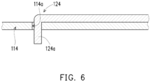
FIG 6 is a cross-sectional view taken along a line II-II of the shielding module inFIG 2 . -
FIG 7 is a flowchart of an assembling method of an shielding module according to an embodiment of the invention. -
FIG 2 is a three-dimensional view of an shielding module according to an embodiment of the invention.FIG 3 is an exploded view of the shielding module inFIG 2 . Referring toFIG 2 andFIG 3 , anshielding module 100 provided by the embodiment includes aframe 110 and acover 120. Theframe 110 is assembled with thecover 120. A material of theframe 110 and thecover 120 is, for example, metal, such that theshielding module 100 may act as an electromagnetic wave shielding module. But the invention is not limited thereto. Theshielding module 100 further includes acircuit board 130. Theframe 110 is soldered onto thecircuit board 130 through, for example, the surface mounting technology (SMT) and is electrically connected to a ground plane of thecircuit board 130, such that masking and shielding are performed to anelectronic element 132 on thecircuit board 130 through theframe 110 and thecover 120. - Specifically, the
frame 110 has anopening 110a, afirst plane 110b, a plurality ofside walls 116, and a first assembling structure. The first assembling structure includes a plurality offirst engagement parts 112 and afirst positioning part 114. Thefirst plane 110b is an outer surface of an upper side of theframe 110 and surrounds and is adjacent to theopening 110a of theframe 110. An area of theopening 110a is larger than an area of thefirst plane 110b. As such, when thecover 120 is detached from theframe 110, the area of theopening 110a of theframe 110 is large enough to expose theelectronic element 132 on the circuit board 130 (shown inFIG 1 ), and that theelectronic element 132 may be repaired or replaced conveniently. Theside walls 116 are connected to a periphery of afirst plane 110b and perpendicular to thefirst plane 110b. A height of each of theside walls 116 is, for example, equal to or slightly greater than a thickness of theelectronic element 132, such that sufficient space is provided for theelectronic element 132 to be disposed therein. The first assembling structure (i.e., each of thefirst engagement parts 112 and the first positioning part 114) is formed on thefirst plane 110b of theframe 110. - The
cover 120 covers theopening 110a of theframe 110 and thefirst plane 110b and has a second assembling structure. The second assembling structure includes a plurality ofsecond engagement parts 122 and asecond positioning part 124. A side of thecover 120 has asecond plane 120a parallel to thefirst plane 110b. Each of thesecond engagement parts 122 and thesecond positioning part 124 are formed on thesecond plane 120a of thecover 120. Thesecond plane 120a is an unbent horizontal plane. An end of the second assembling structure (i.e., each of thesecond engagement parts 122 and the second positioning part 124) extends from thesecond plane 120a to another side of thecover 120. - The second assembling structure (i.e., each of the
second engagement parts 122 and the second positioning parts 124) is assembled with the first assembling structure (i.e., each of thefirst engagement parts 112 and the first positioning part 114) to stop thecover 120 from moving relative to theframe 110. Specifically, each of thesecond engagement parts 122 is engaged with each of thefirst engagement parts 112 in a horizontal direction Y parallel to thefirst plane 110b to stop thecover 120 from moving relative to theframe 110 in a vertical direction Z perpendicular to the horizontal direction Y. Thesecond positioning part 124 is positioned at thefirst positioning part 114 in the vertical direction Z to stop thecover 120 from moving relative to theframe 110 in the horizontal direction Y and to stop thecover 120 from moving relative to theframe 110 in a horizontal direction X. In the embodiment, theelectronic element 132 is disposed on athird plane 130a on thecircuit board 130. Thefirst plane 110b of theframe 110, thesecond plane 120a of thecover 120, and thethird plane 130a of thecircuit board 130 are parallel to each other. - According to such arrangement, each of the
first engagement parts 112 and thefirst positioning part 114 are both formed on an upper plane of the frame 110 (i.e., thefirst plane 110b), and each of thesecond engagement parts 122 and thesecond positioning part 124 are both formed on an upper plane of the cover 120 (i.e., thesecond plane 120a). In theshielding module 100, thefirst engagement parts 112 and thefirst positioning part 114 are respectively matched with thesecond engagement parts 122 and thesecond positioning part 124, and that thecover 120 is fixed on theframe 110 at the upper planes. As such, theframe 110 and thecover 120 are not required to be engaged with each other and be positioned at a lateral surface of theshielding module 100. Thereby, a structure configured to be combined with thecover 120 is not required to be formed at theside walls 116 by theframe 110, and thecover 120 is not required to have a side wall configured to be combined with theframe 110. Therefore, the height of theside walls 116 of theframe 110 may be lowered and a structure of thecover 120 may be simplified to save allocation space and manufacturing costs of an electronic device. Furthermore, the end of the second assembling structure (i.e., each of thesecond engagement parts 122 and the second positioning part 124) extends from the upper plane of the cover 120 (i.e., thesecond plane 120a) toward another side of thecover 120 to prevent the second assembling structure from protruding upward from the upper plane of thecover 120, and thereby a size of theshielding module 100 may be further reduced in the vertical direction. In addition, theframe 110 and thecover 120 are assembled with each other through being engaged with each other as described above and thus may be detached and reworked easily. - In the embodiment, a gap between two adjacent ones of the
first engagement parts 112 is, for example, 2 mm to 7 mm. Correspondingly, a gap between two adjacent ones of thesecond engagement parts 122 is, for example, 2 mm to 7 mm. As such, thecover 120 is securely and tightly engaged with theframe 110, and thereby, electromagnetic wave shielding effect is further enhanced. Nevertheless, the invention is not limited thereto. The gaps between thefirst engagement parts 112 and the gaps between thesecond engagement parts 122 may be changed as required in design. -
FIG 4 is a cross-sectional view taken along a line I-I of the shielding module inFIG 2 . Specifically, in the embodiment, thefirst engagement part 112 includes anotch 112a formed on thefirst plane 110b as shown inFIG 2 to FIG 4 . Thecover 120 has a plurality of openingslots 120b as shown inFIG 2 to FIG 4 . Each of the openingslots 120b is formed on thesecond plane 120a of thecover 120. Each of thesecond engagement parts 122 extends from an inner edge of the corresponding openingslots 120b. As shown inFIG 3 andFIG 4 , thesecond engagement part 122 includes abent section 122a and an engagement section122b. Thebent section 122a is connected between thesecond plane 120a of thecover 120 and theengagement section 122b and is bent relative to thesecond plane 120a, such that theengagement section 122b is engaged with thefirst engagement part 112 through thenotch 112a. -
FIG 5 illustrates the second engagement part separates from the first engagement part inFIG 4 . As shown inFIG 5 , when thesecond engagement part 122 is separated from the first engagement part 112 (as shown inFIG 4 ), an extending direction of theengagement section 122b is inclined relative to thesecond plane 120a. As such, when thesecond engagement part 122 is engaged with thefirst engagement part 112 as shown inFIG 4 , theengagement section 122b is forced and elastically deformed downward. Thereby, an upward holding force may be generated by theengagement section 122b inFIG 4 and applied to thefirst engagement part 112, such that thecover 120 is securely fixed onto theframe 110. As such, even though theframe 110 and thecover 120 provided by the embodiment are engaged and positioned only at the upper plane of the assemblingstructure 100 as described above, a favorable fixing effect may still be achieved. In other embodiments, thefirst engagement part 112 and thesecond engagement part 122 may be other structures that may be engaged with each other. The invention is not limited thereto. -
FIG 6 is a cross-sectional view taken along a line II-II of the shielding module inFIG 2 . Thefirst positioning part 114 provided by the embodiment includes apositioning slot 114a formed on thefirst plane 110b as shown inFIG 2 to FIG 4 . Thesecond positioning part 124 includes abent wall 124a formed on an edge of thecover 120 as shown inFIG 2 to FIG 4 . Thebent wall 124a extends in the vertical direction Z and is adapted to extend into thepositioning slot 114a for positioning. In other embodiments, thefirst positioning part 114 and thesecond positioning part 124 may be other structures that may be positioned with each other. The invention is not limited thereto. - Besides, in the embodiment, the
cover 120 has two extendingparts 126 as shown inFIG 2 andFIG 3 . The two extendingparts 126 are respectively adjacent to opposite sides of thesecond positioning part 124 and adapted to be forced to drive thesecond positioning part 124 to separate from thefirst positioning part 114. Specifically, when a user intends to detach thecover 120, the user may flip the two extendingparts 126 upward. As such, a portion of thecover 120 is elastically deformed and that thebent wall 124a is separated upward from thepositioning slot 114a. Next, thecover 120 is moved in the horizontal direction and thereby, thesecond engagement parts 122 are not engaged with the correspondingfirst engagement parts 112. - An assembling method of the
shielding module 100 provided by the embodiment is described as follows.FIG 7 is a flowchart of an assembling method of an shielding module according to an embodiment of the invention. First, theframe 110 is provided. Theframe 110 has theopening 110a, the at least onefirst engagement part 112 and the first positioning part 114 (step S602). Next, thecover 120 is provided. Thecover 120 has the at least one second engagement part122 and the second positioning part 124 (step S604). Theframe 110 is soldered onto the circuit board 130 (step S606A). After theframe 110 is soldered onto thecircuit board 130, the at least onesecond engagement part 122 is engaged with the at least onefirst engagement part 112 in the horizontal direction Y, and thesecond positioning part 124 is positioned at thefirst positioning part 114 in the vertical direction Z perpendicular to the horizontal direction Y to fix thecover 120 onto the frame 110 (step S608A). - In the embodiment, the
frame 110 has two extendingparts 118 as shown inFIG 3 . Each of the extendingparts 118 extends from thefirst plane 110b into theopening 110a. Before theframe 110 is soldered to thecircuit board 130 as described in step S606A, an attraction force provided by an attraction-force-providing device may be applied to each of the extendingparts 118 of theframe 110. As such, theframe 110 is moved onto thecircuit board 130 for following soldering process to be performed. - In addition, the
second engagement part 122 provided by the embodiment includes an extendingsection 122c as shown inFIG 3 andFIG 4 . The extendingsection 122c is connected to an end of theengagement section 122b and has a guiding inclined surface S1. During the process when thesecond engagement part 122 is engaged with thefirst engagement part 112 as described in step S608A, theengagement section 122b of thesecond engagement part 122 may be guided to be engaged with thefirst engagement part 112 through the inclined surface S1 of thesecond engagement part 122. - Similarly, the
first positioning part 114 provided by the embodiment includes a guiding inclined surface S2 as shown inFIG 3 . During the process when thesecond positioning part 124 is positioned at thefirst positioning part 114 as described in step S608A, thebent wall 124a of thesecond engagement part 124 may be guided to move toward thepositioning slot 114a of thefirst positioning part 114 and positioned at thepositioning slot 114a of thefirst positioning part 114 through the guiding inclined surface S2 of thefirst positioning part 114. - During the assembling process, the
frame 110 is first soldered onto thecircuit board 130 and next thecover 120 is assembled with theframe 110. Nevertheless, the invention is not limited thereto. After step S604 is proceeded, thesecond engagement part 122 may first be engaged with thefirst engagement part 112 in the horizontal direction Y, and thesecond positioning part 114 is positioned at thefirst positioning part 114 in the vertical direction Z perpendicular to the horizontal direction Y, such that thecover 120 is fixed onto the frame 110 (step S606B). Next, after thecover 120 is fixed onto theframe 110, theframe 110 is soldered onto a circuit board 130 (step S608B). In other words, thecover 120 is first assembled with theframe 110 and then theframe 110 is soldered onto thecircuit board 130. Through such an assembling method, in the embodiment, theframe 110 and thecover 120 are not engaged nor positioned at theside walls 116 of theframe 110 as described above. Moreover, as thecover 120 has no side wall, and thereby, during the soldering process, theside walls 116 of theframe 110 may not be in contact with a soldering material, which may lead to thecover 120 is soldered and fixed onto theframe 110 unexpectedly. - Before the
frame 110 is soldered onto thecircuit board 130 as described in step S608B, the attraction force provided by the attraction-force-providing device may first be applied to thecover 120. As such, thecover 120 and theframe 110 are moved onto thecircuit board 130 for following soldering process to be performed. Through such the assembling manner, theframe 110 may not need to have the extendingparts 118 for the attraction force to be applied on. - To sum up, in the shielding module provided by the embodiments of the invention, the first engagement parts and the first positioning part are both formed on the upper plane of the frame (i.e., the first plane). The second engagement parts and the second positioning part are both formed on the upper plane of the cover (i.e., the second plane). In the shielding module, the first engagement parts and the first positioning part are respectively matched with the second engagement parts and the second positioning part, and that the cover is fixed onto the frame at the upper planes. As such, the frame and the cover are not required to be engaged with each other and be positioned at the lateral surface of the shielding module. Thereby, a structure configured to be combined with the cover is not required to be formed at the side walls by the frame, and the cover is not required to have a side wall configured to be combined with the frame either. Therefore, the height of the side walls of the frame may be reduced and the structure of the cover may be simplified to save allocation space and manufacturing costs of the electronic device. Furthermore, the end of the second assembling structure (i.e., each of the second engagement parts and the second positioning part) extends from the upper plane of the cover (i.e., the second plane) to another side of the cover to prevent the second assembling structure from protruding upward from the upper plane of the cover, and thereby, the size of the assembling structure may be further reduced in the vertical direction. In addition, the frame and the cover are assembled with each other through being engaged with each other as described above and thus may be detached and reworked easily.
Claims (10)
- An shielding module (100), comprising:a frame (110), having an opening (110a), a first plane (110b), a plurality of side walls (116), and a first assembling structure, wherein the first plane (110b) surrounds and is adjacent to the opening (110a), an area of the opening (110a) is larger than an area of the first plane (110b), the side walls (116) are connected to a periphery of the first plane (110b), the first assembling structure is entirely formed on the first plane (110b) without extending to the side walls (116), and the first assembling structure comprises at least one first engagement part (112) and a first positioning part (114); anda cover (120), covering the opening (110a) and the first plane (110b) and having a second assembling structure, wherein a side of the cover (120) has a second plane (120a) parallel to the first plane (110b), the second assembling structure is formed on the second plane (120a) and comprises at least one second engagement part (122) and a second positioning part (124), and the cover (120) has no side wall,wherein the second assembling structure is assembled with the first assembling structure to stop the cover (120) from moving relative to the frame (110),the at least one first engagement part (112) and the first positioning part (114) are both formed on the first plane (110b), the at least one second engagement part (122) and the second positioning part (124) are both formed on the second plane (120a), the second engagement part (122) is engaged with the first engagement part (112) to stop the cover (120) from moving in a vertical direction (Z) relative to the frame (110), and the second positioning part (124) is positioned at the first positioning part (114) to stop the cover (120) from moving in the horizontal direction (Y) relative to the frame (110),the at least one first engagement part (112) comprises a notch (112a) formed on the first plane (110b), the at least one second engagement part (122) comprises a bent section (122a) and an engagement section (122b), the bent section (122a) is connected between the second plane (120a) and the engagement section (122b) and bent relative to the second plane (120a), and the engagement section (122b) is engaged with the at least one first engagement part (112) through the notch (112a)wherein the at least one second engagement part (122) further comprises an extending section (122c) connected to an end of the engagement section (122b), the extending section (122c) is inclined relative to the second plane (120a) and has a guiding inclined surface (S1), an extending direction of the engagement section (122b) is inclined relative to the second plane (120a), the extending section (122c) and an end of the second positioning part (124) both extend toward another side of the cover (120) from the second plane (120a) along a direction that is away from the cover (120), the engagement section (122b) is guided through the guiding inclined surface (S1) and elastically deformed, and is engaged with the first engagement part (112) in a horizontal direction (Y) and abuts against a back surface of the frame (110) opposite to the first plane (110a),wherein the first positioning part (114) comprises a positioning slot (114a) formed on the first plane (110b), the second positioning part (124) comprises a bent wall (124a) formed on an edge of the cover (120), and the bent wall (124a) extends in the vertical direction (Z),wherein the first positioning part (114) comprises a guiding inclined surface (S2), and the bent wall (124a) is adapted to move toward the positioning slot (114a) through guiding of the guiding inclined surface (S2).
- The shielding module (100) as claimed in claim 1, wherein the second positioning part (124) is positioned at the first positioning part (114) in the vertical direction (Z).
- The shielding module (100) as claimed in claim 2, wherein the cover (120) has at least one opening slot (120b), the at least one opening slot (120b) is entirely formed on the second plane (120a), and the at least one second engagement part (122) extends from an inner edge of the at least one opening slot (120b).
- The shielding module (100) as claimed in any of the claims 1 to 3, wherein a number of the at least one first engagement part (112) is plural, a gap between two adjacent ones of the first engagement parts (112) is 2 mm to 7 mm, a number of the at least one second engagement part (122) is plural, and a gap between two adjacent ones of the second engagement parts (122) is 2 mm to 7 mm.
- The shielding module (100) as claimed in any of the claims 1 to 4, wherein the cover (120) has at least one extending part (126), and the at least one extending part (126) is adjacent to the second positioning part (124) and is adapted to be forced to drive the second positioning part (124) to separate from the first positioning part (114).
- The shielding module (100) as claimed in any of the claims 1 to 5, wherein the frame (110) has at least one extending part (118), the at least one extending part (118) extends from the first plane (110b) into the opening (110a), and an attraction force is adapted to be applied to the at least one extending part (118) to move the frame (110).
- The shielding module (100) as claimed in any of the claims 1 to 6, wherein and the side walls (116) are perpendicular to the first plane (110b).
- The shielding module (100) as claimed in any of the claims 1 to 7, comprising a circuit board (130), wherein the frame (110) is disposed on the circuit board (130), and the frame (110) and the cover (120) mask at least one electronic element (132) on the circuit board (130).
- The shielding module (100) as claimed in claim 7, wherein the at least one electronic element (132) is disposed on a third plane (130a) on the circuit board (130), and the first plane (110b) and the second plane (120a) are parallel to the third plane (130a).
- The shielding module (100) as claimed in any of the claims claim 1 to 9, wherein a material of the cover (120) and the frame (110) is metal, and the shielding module (100) is an electromagnetic wave shielding module.
Applications Claiming Priority (1)
| Application Number | Priority Date | Filing Date | Title |
|---|---|---|---|
| TW106106349A TWI682707B (en) | 2017-02-24 | 2017-02-24 | Assembling component and assembling method thereof |
Publications (3)
| Publication Number | Publication Date |
|---|---|
| EP3367772A1 EP3367772A1 (en) | 2018-08-29 |
| EP3367772C0 EP3367772C0 (en) | 2025-05-28 |
| EP3367772B1 true EP3367772B1 (en) | 2025-05-28 |
Family
ID=59699471
Family Applications (1)
| Application Number | Title | Priority Date | Filing Date |
|---|---|---|---|
| EP17185233.8A Active EP3367772B1 (en) | 2017-02-24 | 2017-08-08 | Assembling component |
Country Status (4)
| Country | Link |
|---|---|
| US (1) | US10257968B2 (en) |
| EP (1) | EP3367772B1 (en) |
| CN (1) | CN108513522B (en) |
| TW (1) | TWI682707B (en) |
Families Citing this family (2)
| Publication number | Priority date | Publication date | Assignee | Title |
|---|---|---|---|---|
| CN110830625B (en) * | 2019-11-14 | 2021-03-26 | 华勤技术股份有限公司 | Shell and mobile terminal comprising same |
| CN112423469A (en) * | 2021-01-04 | 2021-02-26 | 四川赛狄信息技术股份公司 | Circuit board double-chip centered anti-seismic reinforcing structure and controller circuit board |
Citations (2)
| Publication number | Priority date | Publication date | Assignee | Title |
|---|---|---|---|---|
| US5436802A (en) * | 1994-03-16 | 1995-07-25 | Motorola | Method and apparatus for shielding an electrical circuit that is disposed on a substrate |
| US20060121784A1 (en) * | 2004-12-04 | 2006-06-08 | Hon Hai Precision Industry Co., Ltd. | Electromagnetic interference shield |
Family Cites Families (21)
| Publication number | Priority date | Publication date | Assignee | Title |
|---|---|---|---|---|
| JP2501638Y2 (en) * | 1991-11-25 | 1996-06-19 | 船井電機株式会社 | Shield board for PCB mounting |
| DE19636182A1 (en) * | 1996-09-06 | 1998-03-12 | Philips Patentverwaltung | Shield housing for electronic components |
| US6140577A (en) * | 1998-10-08 | 2000-10-31 | Gateway 2000, Inc | Electronic chassis electro-magnetic interference seal and sealing device |
| US6274808B1 (en) * | 1999-05-06 | 2001-08-14 | Lucent Technologies, Inc. | EMI shielding enclosure |
| CN101340806B (en) | 2007-07-06 | 2012-10-31 | 莱尔德电子材料(上海)有限公司 | Screening arrangement and method for producing the same |
| CN101472453B (en) * | 2007-12-29 | 2012-01-18 | 鸿富锦精密工业(深圳)有限公司 | Electromagnetic shielding device |
| JP2012530758A (en) * | 2009-06-24 | 2012-12-06 | ベーリンガー インゲルハイム インターナショナル ゲゼルシャフト ミット ベシュレンクテル ハフツング | Novel compounds, pharmaceutical compositions and methods relating thereto |
| CN102036540A (en) * | 2009-09-30 | 2011-04-27 | 莱尔德技术股份有限公司 | Shielding shell |
| TWM380706U (en) * | 2009-12-10 | 2010-05-11 | Wistron Corp | Metal shielding casing and the combination thereof with circuit board |
| KR101068550B1 (en) * | 2010-02-03 | 2011-09-30 | 조인셋 주식회사 | Easy soldering shield case for electromagnetic shielding |
| CN201657596U (en) * | 2010-02-03 | 2010-11-24 | 鸿富锦精密工业(深圳)有限公司 | Electromagnetic shielding device |
| CN201657591U (en) * | 2010-03-08 | 2010-11-24 | 国基电子(上海)有限公司 | Electromagnetic screen |
| GB2498662B (en) * | 2010-09-07 | 2015-04-01 | Caged Idea S Llc | Data transmission blocking holder |
| CN102548371B (en) * | 2010-12-15 | 2015-02-04 | 和硕联合科技股份有限公司 | Electromagnetic shielding module |
| KR101062484B1 (en) * | 2011-05-26 | 2011-09-05 | 주식회사 성덕전자 | Electromagnetic shielding shield |
| US20130250540A1 (en) * | 2012-03-21 | 2013-09-26 | Chih-Yuan Hou | Shielding shell |
| TWI548338B (en) * | 2012-08-07 | 2016-09-01 | 緯創資通股份有限公司 | Shielding device and electronic device with the same |
| TW201410132A (en) * | 2012-08-16 | 2014-03-01 | Wistron Corp | Shielding can assembly |
| US9462732B2 (en) * | 2013-03-13 | 2016-10-04 | Laird Technologies, Inc. | Electromagnetic interference shielding (EMI) apparatus including a frame with drawn latching features |
| CN105451528A (en) * | 2014-08-18 | 2016-03-30 | 国基电子(上海)有限公司 | Shielding device |
| CN205847842U (en) * | 2016-06-03 | 2016-12-28 | 上海与德通讯技术有限公司 | Mainboard shielding construction and the mobile terminal with mainboard shielding construction |
-
2017
- 2017-02-24 TW TW106106349A patent/TWI682707B/en active
- 2017-03-16 CN CN201710158071.8A patent/CN108513522B/en active Active
- 2017-06-02 US US15/611,794 patent/US10257968B2/en active Active
- 2017-08-08 EP EP17185233.8A patent/EP3367772B1/en active Active
Patent Citations (2)
| Publication number | Priority date | Publication date | Assignee | Title |
|---|---|---|---|---|
| US5436802A (en) * | 1994-03-16 | 1995-07-25 | Motorola | Method and apparatus for shielding an electrical circuit that is disposed on a substrate |
| US20060121784A1 (en) * | 2004-12-04 | 2006-06-08 | Hon Hai Precision Industry Co., Ltd. | Electromagnetic interference shield |
Also Published As
| Publication number | Publication date |
|---|---|
| CN108513522B (en) | 2020-04-28 |
| US20180249598A1 (en) | 2018-08-30 |
| EP3367772C0 (en) | 2025-05-28 |
| TW201832640A (en) | 2018-09-01 |
| US10257968B2 (en) | 2019-04-09 |
| CN108513522A (en) | 2018-09-07 |
| EP3367772A1 (en) | 2018-08-29 |
| TWI682707B (en) | 2020-01-11 |
Similar Documents
| Publication | Publication Date | Title |
|---|---|---|
| US6949706B2 (en) | Radio frequency shield for electronic equipment | |
| US6943287B2 (en) | Shielding cage with improved EMI shielding gasket construction | |
| US9247682B2 (en) | Electronic circuit module | |
| EP1930995A2 (en) | Electrical connector | |
| US8558121B2 (en) | Electronic device having an electromagnetic shield | |
| JP4348725B2 (en) | Socket for mounting electronic parts | |
| US6985366B2 (en) | EMC shield and housing for electronic components | |
| US8520405B2 (en) | Shield case and image display device | |
| KR20130068901A (en) | Apparatus of shield can for device and manufacturing method thereof | |
| US20090268420A1 (en) | Shielding assembly | |
| US20110073360A1 (en) | Shielding enclosures | |
| US8462519B2 (en) | Method of shielding a circuit board, circuit board, electromagnetic shield and method of manufacturing same | |
| CN101340806A (en) | Shielding device and method of manufacturing shielding device | |
| JP2006165201A (en) | Circuit module device | |
| US10257968B2 (en) | Assembling component and assembling method thereof | |
| KR101454485B1 (en) | Shield cans of mobile terminals | |
| JP5224407B2 (en) | Shield case and electronic equipment | |
| CN101742895A (en) | Shielding Structure of Electronic Devices | |
| JP4182529B2 (en) | Electronic component mounting socket and contact carrier used therefor | |
| JPH1126973A (en) | Electronic apparatus | |
| KR20220138821A (en) | Substrate Connector | |
| JP2003163485A (en) | Structure for shielding sub-rack | |
| JP2014086479A (en) | Electronic apparatus | |
| JP2005294436A (en) | Shield structure of electronic equipment |
Legal Events
| Date | Code | Title | Description |
|---|---|---|---|
| PUAI | Public reference made under article 153(3) epc to a published international application that has entered the european phase |
Free format text: ORIGINAL CODE: 0009012 |
|
| STAA | Information on the status of an ep patent application or granted ep patent |
Free format text: STATUS: REQUEST FOR EXAMINATION WAS MADE |
|
| 17P | Request for examination filed |
Effective date: 20170808 |
|
| AK | Designated contracting states |
Kind code of ref document: A1 Designated state(s): AL AT BE BG CH CY CZ DE DK EE ES FI FR GB GR HR HU IE IS IT LI LT LU LV MC MK MT NL NO PL PT RO RS SE SI SK SM TR |
|
| AX | Request for extension of the european patent |
Extension state: BA ME |
|
| STAA | Information on the status of an ep patent application or granted ep patent |
Free format text: STATUS: EXAMINATION IS IN PROGRESS |
|
| 17Q | First examination report despatched |
Effective date: 20191023 |
|
| GRAP | Despatch of communication of intention to grant a patent |
Free format text: ORIGINAL CODE: EPIDOSNIGR1 |
|
| STAA | Information on the status of an ep patent application or granted ep patent |
Free format text: STATUS: GRANT OF PATENT IS INTENDED |
|
| INTG | Intention to grant announced |
Effective date: 20250219 |
|
| GRAS | Grant fee paid |
Free format text: ORIGINAL CODE: EPIDOSNIGR3 |
|
| GRAA | (expected) grant |
Free format text: ORIGINAL CODE: 0009210 |
|
| STAA | Information on the status of an ep patent application or granted ep patent |
Free format text: STATUS: THE PATENT HAS BEEN GRANTED |
|
| AK | Designated contracting states |
Kind code of ref document: B1 Designated state(s): AL AT BE BG CH CY CZ DE DK EE ES FI FR GB GR HR HU IE IS IT LI LT LU LV MC MK MT NL NO PL PT RO RS SE SI SK SM TR |
|
| REG | Reference to a national code |
Ref country code: GB Ref legal event code: FG4D |
|
| REG | Reference to a national code |
Ref country code: CH Ref legal event code: EP |
|
| REG | Reference to a national code |
Ref country code: IE Ref legal event code: FG4D Ref country code: DE Ref legal event code: R096 Ref document number: 602017089652 Country of ref document: DE |
|
| U01 | Request for unitary effect filed |
Effective date: 20250528 |
|
| U07 | Unitary effect registered |
Designated state(s): AT BE BG DE DK EE FI FR IT LT LU LV MT NL PT RO SE SI Effective date: 20250605 |
|
| U20 | Renewal fee for the european patent with unitary effect paid |
Year of fee payment: 9 Effective date: 20250825 |
|
| PG25 | Lapsed in a contracting state [announced via postgrant information from national office to epo] |
Ref country code: ES Free format text: LAPSE BECAUSE OF FAILURE TO SUBMIT A TRANSLATION OF THE DESCRIPTION OR TO PAY THE FEE WITHIN THE PRESCRIBED TIME-LIMIT Effective date: 20250528 |
|
| PG25 | Lapsed in a contracting state [announced via postgrant information from national office to epo] |
Ref country code: GR Free format text: LAPSE BECAUSE OF FAILURE TO SUBMIT A TRANSLATION OF THE DESCRIPTION OR TO PAY THE FEE WITHIN THE PRESCRIBED TIME-LIMIT Effective date: 20250829 Ref country code: NO Free format text: LAPSE BECAUSE OF FAILURE TO SUBMIT A TRANSLATION OF THE DESCRIPTION OR TO PAY THE FEE WITHIN THE PRESCRIBED TIME-LIMIT Effective date: 20250828 |
|
| PG25 | Lapsed in a contracting state [announced via postgrant information from national office to epo] |
Ref country code: PL Free format text: LAPSE BECAUSE OF FAILURE TO SUBMIT A TRANSLATION OF THE DESCRIPTION OR TO PAY THE FEE WITHIN THE PRESCRIBED TIME-LIMIT Effective date: 20250528 |
|
| PG25 | Lapsed in a contracting state [announced via postgrant information from national office to epo] |
Ref country code: HR Free format text: LAPSE BECAUSE OF FAILURE TO SUBMIT A TRANSLATION OF THE DESCRIPTION OR TO PAY THE FEE WITHIN THE PRESCRIBED TIME-LIMIT Effective date: 20250528 |
|
| PG25 | Lapsed in a contracting state [announced via postgrant information from national office to epo] |
Ref country code: RS Free format text: LAPSE BECAUSE OF FAILURE TO SUBMIT A TRANSLATION OF THE DESCRIPTION OR TO PAY THE FEE WITHIN THE PRESCRIBED TIME-LIMIT Effective date: 20250828 |
|
| PG25 | Lapsed in a contracting state [announced via postgrant information from national office to epo] |
Ref country code: IS Free format text: LAPSE BECAUSE OF FAILURE TO SUBMIT A TRANSLATION OF THE DESCRIPTION OR TO PAY THE FEE WITHIN THE PRESCRIBED TIME-LIMIT Effective date: 20250928 |
|
| PG25 | Lapsed in a contracting state [announced via postgrant information from national office to epo] |
Ref country code: SM Free format text: LAPSE BECAUSE OF FAILURE TO SUBMIT A TRANSLATION OF THE DESCRIPTION OR TO PAY THE FEE WITHIN THE PRESCRIBED TIME-LIMIT Effective date: 20250528 |
|
| PG25 | Lapsed in a contracting state [announced via postgrant information from national office to epo] |
Ref country code: CZ Free format text: LAPSE BECAUSE OF FAILURE TO SUBMIT A TRANSLATION OF THE DESCRIPTION OR TO PAY THE FEE WITHIN THE PRESCRIBED TIME-LIMIT Effective date: 20250528 |
|
| PG25 | Lapsed in a contracting state [announced via postgrant information from national office to epo] |
Ref country code: SK Free format text: LAPSE BECAUSE OF FAILURE TO SUBMIT A TRANSLATION OF THE DESCRIPTION OR TO PAY THE FEE WITHIN THE PRESCRIBED TIME-LIMIT Effective date: 20250528 |
|
| REG | Reference to a national code |
Ref country code: CH Ref legal event code: H13 Free format text: ST27 STATUS EVENT CODE: U-0-0-H10-H13 (AS PROVIDED BY THE NATIONAL OFFICE) Effective date: 20260324 |
|
| PG25 | Lapsed in a contracting state [announced via postgrant information from national office to epo] |
Ref country code: MC Free format text: LAPSE BECAUSE OF FAILURE TO SUBMIT A TRANSLATION OF THE DESCRIPTION OR TO PAY THE FEE WITHIN THE PRESCRIBED TIME-LIMIT Effective date: 20250528 |
|
| PLBE | No opposition filed within time limit |
Free format text: ORIGINAL CODE: 0009261 |
|
| STAA | Information on the status of an ep patent application or granted ep patent |
Free format text: STATUS: NO OPPOSITION FILED WITHIN TIME LIMIT |
|
| REG | Reference to a national code |
Ref country code: CH Ref legal event code: L10 Free format text: ST27 STATUS EVENT CODE: U-0-0-L10-L00 (AS PROVIDED BY THE NATIONAL OFFICE) Effective date: 20260409 |
|
| PG25 | Lapsed in a contracting state [announced via postgrant information from national office to epo] |
Ref country code: CH Free format text: LAPSE BECAUSE OF NON-PAYMENT OF DUE FEES Effective date: 20250831 |
|
| GBPC | Gb: european patent ceased through non-payment of renewal fee |
Effective date: 20250828 |
|
| 26N | No opposition filed |
Effective date: 20260303 |