JP2005294436A - Shield structure of electronic equipment - Google Patents
Shield structure of electronic equipment Download PDFInfo
- Publication number
- JP2005294436A JP2005294436A JP2004105608A JP2004105608A JP2005294436A JP 2005294436 A JP2005294436 A JP 2005294436A JP 2004105608 A JP2004105608 A JP 2004105608A JP 2004105608 A JP2004105608 A JP 2004105608A JP 2005294436 A JP2005294436 A JP 2005294436A
- Authority
- JP
- Japan
- Prior art keywords
- shield case
- ground pattern
- shield
- wiring board
- electronic device
- Prior art date
- Legal status (The legal status is an assumption and is not a legal conclusion. Google has not performed a legal analysis and makes no representation as to the accuracy of the status listed.)
- Pending
Links
Images
Landscapes
- Shielding Devices Or Components To Electric Or Magnetic Fields (AREA)
Abstract
【課題】 配線基板に実装された電子部品を、上記配線基板のグランドパターンと導通したシールドケースに収容して、電子部品からの電磁波を遮蔽するよう構成した電子機器のシールド構造を対象とし、その目的は配線基板やシールドケースの反りに起因するシールド性の低下を未然に防止し得る電子機器のシールド構造を提供することにある。
【解決手段】 本発明は、シールドケースにおける周縁の一部に形成したハンダ接続部を、グランドパターンの一部とハンダ付けして導通させるとともに、ハンダ接続部を除くシールドケースの周縁に形成した弾性接続部を、電子機器構成部材のリブによりシールドケースの天板を押圧してグランドパターンに圧接することで導通させるよう構成している。
【選択図】 図3PROBLEM TO BE SOLVED: To provide a shield structure for an electronic device in which an electronic component mounted on a wiring board is accommodated in a shield case electrically connected to the ground pattern of the wiring board so as to shield an electromagnetic wave from the electronic component. An object of the present invention is to provide a shield structure for an electronic device that can prevent a decrease in shielding performance due to warping of a wiring board or a shield case.
The present invention provides a solder connection portion formed on a part of the peripheral edge of a shield case to be electrically connected to a part of a ground pattern, and has an elasticity formed on the peripheral edge of the shield case excluding the solder connection portion. The connecting portion is configured to be conducted by pressing the top plate of the shield case with the rib of the electronic device component member and pressing the connecting plate against the ground pattern.
[Selection] Figure 3
Description
本発明は、電子機器のシールド構造に関し、詳しくは配線基板に実装された電子部品を、上記配線基板のグランドパターンと導通したシールドケースに収容して、上記電子部品からの電磁波を遮蔽するよう構成した電子機器のシールド構造に関する。 The present invention relates to a shield structure for an electronic device, and more particularly, an electronic component mounted on a wiring board is accommodated in a shield case that is electrically connected to a ground pattern of the wiring board, and is configured to shield electromagnetic waves from the electronic component. The present invention relates to a shield structure for electronic equipment.
例えば、携帯電話機等の各種電子機器においては、作動中に電子部品/電子回路から発生する電磁波が、他の電子機器の作動に悪影響を及ぼす等の事象を防止するべく、様々なEMI(Electro Magnetic Intereference)シールド構造が採用されている。 For example, in various electronic devices such as mobile phones, various EMIs (Electro Magnetic) are used to prevent events such as electromagnetic waves generated from electronic components / electronic circuits during operation to adversely affect the operation of other electronic devices. Intereference) Shield structure is adopted.
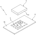
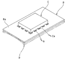
図8および図9に示す従来のシールド構造Aでは、配線基板Bに実装された各電子部品Ea、Ebの電磁波遮蔽を目的として、これら電子部品Ea、Ebを収容する態様で、上記配線基板BにシールドケースCが組み付けられている。 In the conventional shield structure A shown in FIGS. 8 and 9, the wiring board B is configured in such a manner that the electronic parts Ea and Eb are accommodated for the purpose of shielding the electromagnetic waves of the electronic parts Ea and Eb mounted on the wiring board B. A shield case C is assembled to the housing.
配線基板Bの表面Baには、上記電子部品Ea、Ebの周囲を囲う態様でグランドパターンG、G…が形成されている一方、シールドケースCの下方縁部には、上記グランドパターンG、G…に対応した足片Ca、Ca…が形成されており、電子部品Ea、Ebを収容しつつシールドケースCを配線基板B上の所定位置に組み付け、各々の足片Ca、Ca…を各々のグランドパターンG、G…にハンダ付けし、シールドケースCをグランドパターンG、G…とを導通させることで電子部品Ea、Ebの電磁波遮蔽を行なっている。 On the surface Ba of the wiring board B, ground patterns G, G... Are formed so as to surround the electronic components Ea, Eb. On the lower edge of the shield case C, the ground patterns G, G are formed. .. Corresponding to... Are formed, the shield case C is assembled at a predetermined position on the wiring board B while accommodating the electronic components Ea, Eb, and the respective foot pieces Ca, Ca,. The electronic components Ea and Eb are shielded from electromagnetic waves by soldering the ground patterns G, G... And making the shield case C conductive with the ground patterns G, G.
ここで、出願人の知っている上述の如き先行技術は、公知・公用の技術であって文献公知発明に係わるものではなく、もって記載すべき先行技術文献情報はない。 Here, the above-mentioned prior art known to the applicant is a publicly known / public technique, and does not relate to the literature known invention, and there is no prior art document information to be described.
ところで、電子部品Ea、Ebを実装している配線基板Bにおいては、その構造特性や製造プロセスに起因して、図9中に鎖線で示す如く「反り」が生じることは避けられない。また、薄板板金から形成されるシールドケースCにおいても、配線基板Bと同じく「反り」が生じることは避けられない。 Incidentally, in the wiring board B on which the electronic components Ea and Eb are mounted, it is inevitable that “warping” occurs as shown by a chain line in FIG. 9 due to the structural characteristics and the manufacturing process. Further, in the shield case C formed of a thin sheet metal, it is inevitable that “warping” occurs as in the case of the wiring board B.
このため、配線基板BやシールドケースCの「反り」が特に大きい場合には、配線基板Bの表面Baに形成されたグランドパターンG、G…と、シールドケースCの下縁に形成された足片Ca、Ca…との間に部分的な隙間が生じることで未ハンダが起こり、これによってシールドケースCとグランドパターンG、G…との導通が不確実となるために、シールド性(電磁波遮蔽性)の大幅な低下を招いてしまう不都合があった。 Therefore, when the “warping” of the wiring board B or the shield case C is particularly large, the ground patterns G, G... Formed on the surface Ba of the wiring board B and the legs formed on the lower edge of the shield case C are used. Since a partial gap is generated between the pieces Ca, Ca..., Unsoldering occurs, which causes uncertain conduction between the shield case C and the ground patterns G, G. There was a disadvantage that caused a significant decrease in the property.
上記実状に鑑みて本発明の目的は、配線基板やシールドケースの「反り」に起因するシールド性の低下を未然に防止することの可能な電子機器のシールド構造を提供することにある。 In view of the above situation, an object of the present invention is to provide a shield structure for an electronic device that can prevent a decrease in shielding property due to “warping” of a wiring board or a shield case.
上記目的を達成するべく、本発明に関わる電子機器のシールド構造は、配線基板の表面に電磁波遮蔽を要する電子部品の周囲を巡る態様でグランドパターンを形成し、該グランドパターンと互いに導通しかつ前記電子部品を収容する態様で、配線基板にシールドケースを組み付けて成る電子機器のシールド構造であって、シールドケースにおける周縁の一部に、グランドパターンの一部に対向したハンダ接続部を形成するとともに、該ハンダ接続部を除くシールドケースの周縁に、グランドパターンに対向した弾性接続部を設ける一方、シールドケースの天板に臨む電子機器構成部材に、シールドケースの天板に当接して弾性接続部をグランドパターンに圧接させるリブを形成し、シールドケースにおけるハンダ接続部をグランドパターンとハンダ付けするとともに、シールドケースにおける弾性接続部をリブによってグランドパターンに圧接することにより、シールドケースとグランドパターンとを互いに導通させるよう構成したことを特徴としている。 In order to achieve the above object, the shield structure for an electronic device according to the present invention forms a ground pattern on the surface of the wiring board around the electronic component that needs to be shielded against electromagnetic waves, and is electrically connected to the ground pattern. An electronic device shielding structure in which a shielding case is assembled to a wiring board in a manner of accommodating electronic components, and a solder connection portion facing a part of the ground pattern is formed on a part of the periphery of the shielding case. The elastic connection portion is provided at the periphery of the shield case excluding the solder connection portion, and is opposed to the ground pattern, while the electronic device component facing the top plate of the shield case is in contact with the top plate of the shield case. Forming a rib that presses against the ground pattern, and connecting the solder connection in the shield case to the ground pattern. As well as with Sunda, by pressing the resilient connecting portion in the shield case to the ground pattern by the ribs, it is characterized by being configured so as to conduct the shield case and the ground pattern from each other.
本発明に関わる電子機器のシールド構造では、シールドケースの一部に設けたハンダ接続部をグランドパターンにハンダ付けするとともに、シールドケースに形成した弾性接続部を、電子機器構成部品に設けたリブによってグランドパターンに圧接しているため、弾性接続部が配線基板の「反り」に倣って適宜に弾性変形することで、配線基板上のグランドパターンとの間に隙間ができず、もってシールドケースとグランドパターンとの導通不良に起因する、シールド性の低下を未然に防止することが可能となる。 In the shield structure of the electronic device according to the present invention, the solder connection portion provided in a part of the shield case is soldered to the ground pattern, and the elastic connection portion formed in the shield case is provided by the rib provided in the electronic device component. Since it is pressed against the ground pattern, the elastic connection part will be elastically deformed appropriately following the “warp” of the wiring board, so there will be no gap between it and the ground pattern on the wiring board. It is possible to prevent a decrease in shielding property due to poor conduction with the pattern.
また、本発明に関わる電子機器のシールド構造では、シールドケースのハンダ接続部をグランドパターンにハンダ付けしているため、配線基板に対するシールドケースの位置ずれを未然に防止することができ、もって電子機器を生産する際における不良品の発生率や、使用時における不具合の発生率を抑えることが可能となる。 Further, in the shield structure of the electronic device according to the present invention, since the solder connection part of the shield case is soldered to the ground pattern, it is possible to prevent the positional displacement of the shield case with respect to the wiring board. It is possible to reduce the rate of occurrence of defective products during production and the rate of occurrence of defects during use.
以下、実施例を示す図面に基づいて、本発明を詳細に説明する。
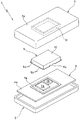
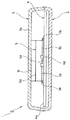
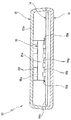
図1〜図3は、本発明に関わる電子機器のシールド構造を、電子機器の一態様である携帯電話機に適用した第1の実施例を示しており、この携帯電話機1は互いに組み付けられて筐体を構成する前面ケース2および背面ケース3と、上記筐体の内部に収容設置される配線基板4と、この配線基板4の実装面(上面)4aに組み付けられるシールドケース5とを具備している。
Hereinafter, the present invention will be described in detail with reference to the drawings illustrating embodiments.
1 to 3 show a first embodiment in which the shield structure of an electronic device according to the present invention is applied to a mobile phone which is an aspect of the electronic device. A
上記配線基板4は、前面ケース2における内部の所定位置に取り付けられており、また上記配線基板4には所望の電子回路を構築する種々の電子部品が実装され、その実装面4aには電磁波遮蔽を要する電子部品Ea、Ebの周囲を巡る態様で、後述するシールドケース5に対応した四角い枠形状を呈するグランドパターン4gが形成されている。
The
一方、シールドケース5は、電磁波遮蔽を要する電子部品Ea、Ebを覆う態様で配線基板4に組み付けられており、例えばステンレス等の薄肉板金を曲げ成形や絞り成形することによって作成され、矩形状を成す天板5tと、該天板5tの各片から下方に展開する前後左右の側板5s、5s…とを有する底部の開放された箱形状を呈している。
On the other hand, the
また、上記シールドケース5における周縁の一部、詳しくは、1つの側板5sにおける下縁の中央域には、左右の切欠きにより区画されて下方に延びる平板状のハンダ接続舌片(ハンダ接続部)5aが形成されている。
Further, a part of the peripheral edge of the
さらに、上記シールドケース5におけるハンダ接続舌片5aを除く周縁、詳しくは、ハンダ接続舌片5aが形成された側板5sの上記ハンダ接続舌片5a以外の下縁、およびハンダ接続舌片5aの形成されていない3つの側板5sの下縁には、それぞれ湾曲したバネ形状を呈する弾性接続舌片(弾性接続部)5bが形成されている。
Further, the periphery of the
ここで、上記シールドケース5が配線基板4に対する所定の位置に組み付けられた状態では、上述したハンダ接続舌片5aと各弾性接続舌片5b、5b…とが、配線基板4におけるグランドパターン4g上に位置している。
Here, in a state where the
さらに、上記シールドケース5が配線基板4に対する所定の位置に組み付けられた状態において、上記ハンダ接続舌片5aは、上記グランドパターン4gの一部とハンダ付けされることによって機械的かつ電気的に接続されている。
Further, in a state where the
一方、上記配線基板4に組み付けられたシールドケース5の天板5tに臨む、背面ケース3における底板(電子機器構成部材)3aには、上記シールドケース5における天板5tの周縁に対応した、四角い枠形状を呈するリブ3rが突出形成されている。
On the other hand, the bottom plate (electronic device constituent member) 3a in the
上記リブ3rは、天板5tに当接してシールドケース5を配線基板4に接近する方向へ押圧するものであり、これによってシールドケース5における各弾性接続舌片5b、5b…は、配線基板4におけるグランドパターン4gに圧接されることとなる。
The
ここで、シールドケース5の弾性接続舌片5bを、背面ケース3に設けたリブ3rによってグランドパターン4gに圧接することで、各弾性接続舌片5bは配線基板4の「反り」に倣って適宜に弾性変形するため、グランドパターン4gとの間に不用意な隙間を生じることがなく、もって各弾性接続舌片5bがグランドパターン4gと確実に接触して導通することとなる。
Here, the elastic connecting
このように、シールドケース5のハンダ接続舌片5aを、配線基板4のグランドパターン4gにハンダ付けするとともに、シールドケース5の弾性接続舌片5bを、背面ケース3のリブ3rによって、配線基板4のグランドパターン4gに圧接させることで、配線基板4やシールドケース5の「反り」に起因するグランドパターン4gとシールドケース5との導通不良が払拭され、もってシールド性の低下を未然に防止することが可能となる。
In this way, the
また、上述したシールド構造を採用した携帯電話機1の製造工程は、配線基板4にシールドケース5を組み付け、グランドパターン4gにハンダ接続舌片5aをハンダ付けしたのち、配線基板4を前面ケース2の所定位置に取り付け、次いで背面ケース3を前面ケース2に組み付けることとなるが、上述の如くシールドケース5のハンダ接続舌片5aをグランドパターン4gにハンダ付けしているので、それ以降の工程においては配線基板4に対するシールドケース5の位置ずれが防止され、もって携帯電話機1の生産時における不良品の発生率や、使用時における不具合の発生率を可及的に抑えることができる。
Further, in the manufacturing process of the
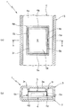
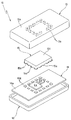
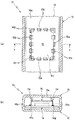
図4〜図6は、本発明に関わる電子機器のシールド構造を、電子機器の一態様である携帯電話機に適用した第2の実施例を示しており、この携帯電話機10は互いに組み付けられて筐体を構成する前面ケース12および背面ケース13と、上記筐体の内部に収容設置される配線基板14と、この配線基板14の実装面(上面)14aに組み付けられるシールドケース15とを具備している。
4 to 6 show a second embodiment in which the shield structure of an electronic device according to the present invention is applied to a mobile phone which is an aspect of the electronic device. The
上記配線基板14は、前面ケース12における内部の所定位置に取り付けられており、また上記配線基板14には、所望の電子回路を構築する種々の電子部品が実装され、その実装面14aには、電磁波遮蔽を要する電子部品Ea、Ebの周囲を巡る態様で、所定個数のグランドパターン14g、14g…が、後述するシールドケース15と対応したレイアウトで形成されている。
The
一方、シールドケース15は、電磁波遮蔽を要する電子部品Ea、Ebを覆う態様で配線基板14に組み付けられており、例えばステンレス等の薄肉板金を曲げ成形や絞り成形することによって作成され、矩形状を成す天板15tと、該天板15tの各片から下方に展開する前後左右の側板15s、15s…とを有する底部の開放された箱形状を呈している。
On the other hand, the
また、上記シールドケース15における周縁の一部、詳しくは、1つの側板15sにおける下縁の中央域には、左右の切欠きにより区画されて下方に延びる平板状のハンダ接続舌片(ハンダ接続部)15aが形成されている。
Further, a part of the peripheral edge of the
さらに、上記シールドケース15におけるハンダ接続舌片15aを除く周縁、詳しくは、ハンダ接続舌片15aが形成された側板15sの上記ハンダ接続舌片5a以外の下縁、およびハンダ接続舌片15aの形成されていない3つの側板15sの下縁には、湾曲したバネ形状を呈する弾性接続舌片(弾性接続部)15bが、それぞれ所定の個数ずつ任意のピッチで間欠形成されている。
Further, the peripheral edge of the
ここで、上記シールドケース15が配線基板14に対する所定の位置に組み付けられた状態では、上述したハンダ接続舌片15aと各弾性接続舌片15b、15b…とが、それぞれ配線基板14における各グランドパターン14g上に位置している。
Here, in a state where the
さらに、上記シールドケース15が配線基板14に対する所定の位置に組み付けられた状態において、上記ハンダ接続舌片15aは、1つのグランドパターン14gとハンダ付けされることによって機械的かつ電気的に接続されている。
Further, in a state where the
一方、上記配線基板14に組み付けられたシールドケース15の天板15tに臨む、背面ケース13における底板(電子機器構成部材)13aには、上記シールドケース15における天板15tの周縁、詳しくは、シールドケース15における各弾性接続舌片15b、15b…の上方部のみと当接するレイアウトで、所定個数のリブ13r、13r…が突出形成されている。
On the other hand, the bottom plate (electronic device constituent member) 13a in the
上記リブ13r、13r…は、天板15tに当接してシールドケース15を配線基板14に接近する方向へ押圧するものであり、これによってシールドケース15の各弾性接続舌片15b、15b…は、配線基板14の各グランドパターン14g、14g…に圧接されることとなる。
The
ここで、シールドケース15の弾性接続舌片15bを、背面ケース13に設けたリブ13rによってグランドパターン14gに圧接することで、各弾性接続舌片15bは配線基板14の「反り」に倣って適宜に弾性変形するため、グランドパターン14gとの間に不用意な隙間を生じることがなく、もって各弾性接続舌片15bが各グランドパターン14gと確実に接触して導通することとなる。
Here, the elastic connecting
このように、シールドケース15のハンダ接続舌片15aを、配線基板14のグランドパターン14gにハンダ付けするとともに、シールドケース15の弾性接続舌片15bを、背面ケース13のリブ13rによって、配線基板14のグランドパターン14gに圧接させることで、配線基板14やシールドケース15の「反り」に起因するグランドパターン14gとシールドケース15との導通不良が払拭され、もってシールド性の低下を未然に防止することが可能となる。
In this manner, the
また、上述したシールド構造を採用した携帯電話機10の製造工程は、配線基板14にシールドケース15を組み付け、グランドパターン14gにハンダ接続舌片15aをハンダ付けしたのち、配線基板14を前面ケース12の所定位置に取り付け、次いで背面ケース13を前面ケース12に組み付けることとなるが、上述の如くシールドケース15のハンダ接続舌片15aをグランドパターン14gにハンダ付けしているので、それ以降の工程においては配線基板14に対するシールドケース15の位置ずれが防止され、もって携帯電話機10の生産時における不良品の発生率や、使用時における不具合の発生率を可及的に抑えることができる。
Further, in the manufacturing process of the
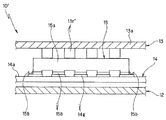
図7に示す、本発明のシールド構造を適用した携帯電話機10では、背面ケース13の底板13aにおける所定個数のリブ13r′、13r′…が、それぞれシールドケース15において隣り合う弾性接続舌片15b、15bの間の上方部のみを押圧するレイアウトで形成されている。
In the
なお、上述した携帯電話機10′の構成は、リブ13r′、13r′…のレイアウト以外、図4〜図6に示した携帯電話機10と基本的に同一なので、図7に示す携帯電話機10′の構成要素において、携帯電話機10の構成要素と同一の作用を成すものには、図4〜図6と同一の記号を附すことで詳細な説明は省略する。
The configuration of the mobile phone 10 'described above is basically the same as that of the
上述した構成における携帯電話機10′のシールド構造においても、図4〜図6に示した携帯電話機10と同様、配線基板14やシールドケース15の「反り」に起因するグランドパターン14gとシールドケース15との導通不良を払拭し得る等の作用効果を奏することは言うまでもない。
Also in the shield structure of the
また、上述した携帯電話機10′のシールド構造では、背面ケース13のリブ13r′によって上方から押下することで、シールドケース15の隣り合う弾性接続舌片15b、15bの間が、これら弾性接続舌片15b、15bを支点とした梁の如く下方へ撓むこととなり、この部位に生じる弾性復帰力も加わって、各弾性接続舌片15b、15b…はグランドパターン14gに強く圧接するため、シールドケース15とグランドパターン14gとの導通がさらに確実なものとなる。
Further, in the above-described shield structure of the
また、各リブ13r′、13r′…の長さが不揃いであったり、シールドケース15の高さ寸法が均一でない場合でも、リブ13r′による押下力が左右の弾性接続舌片15b、15bへ適宜に分配されることで、各弾性接続舌片15bの変形によって上記寸法のバラツキが吸収され、もってシールドケース15とグランドパターン14gとの導通が確実に為されることとなる。
Further, even when the lengths of the
なお、図1〜図3に示した第1の実施例におけるシールド構造では、グランドパターン4gが連続した枠形状を呈し、シールドケース5の弾性接続舌片5bは側板5sの下縁に沿って延在し、リブ3rは連続した枠形状を呈している一方、図4〜図6に示した第2の実施例におけるシールド構造では、グランドパターン14g、14g…が飛び石状に配設され、シールドケース15の弾性接続舌片15b、15b…が側板15sの下縁に沿って所定のピッチで配列形成され、さらにリブ13r、13r…も所定のピッチで配列形成されているが、このように複数の形態を有するグランドパターンとシールドケースとリブとの組合せは、上述した第1および第2の実施例に限定されるものではない。
In the shield structure in the first embodiment shown in FIGS. 1 to 3, the
すなわち、配線基板に連続した枠形状のグランドパターンを形成し、シールドケースには所定のピッチで複数の弾性接続舌片を配列形成するとともに、リブを所定のピッチで配列形成する、あるいはリブを連続した枠形状に形成する等、グランドパターンとシールドケースとリブの形態を、電子機器における設計仕様等の諸条件に基づいて適宜に組み合わせ、もって任意のシールド構造を構築することが可能である。 That is, a continuous frame-shaped ground pattern is formed on the wiring board, and a plurality of elastic connecting tongues are arranged on the shield case at a predetermined pitch, and ribs are arranged at a predetermined pitch, or the ribs are continuous. It is possible to construct an arbitrary shield structure by appropriately combining the forms of the ground pattern, the shield case, and the ribs based on various conditions such as the design specifications of the electronic device, such as forming the frame shape.
また、上述した実施例においては、配線基板の略中央域に1個のシールドケースを組み付けた例を示したが、例えば配線基板の短辺方向に沿って2個のシールドケースを並べて設置する等、様々なレイアウトの電子機器に対しても、本発明を有効に適用し得ることは言うまでもない。 In the above-described embodiment, an example in which one shield case is assembled in the substantially central region of the wiring board is shown. For example, two shield cases are arranged side by side along the short side direction of the wiring board. Needless to say, the present invention can be effectively applied to electronic devices having various layouts.
また、上述した各実施例においては、シールドケースの一部に、グランドパターンとのハンダ付けに供される、特化した形状のハンダ接続部(ハンダ接続舌片)を形成しているが、シールドケースにおける下縁の全周に亘って弾性接続部を形成し、この弾性接続部の一部をグランドパターンとハンダ付けすることで、上記弾性接続部(一部)をハンダ接続部として利用することも可能である。 Further, in each of the above-described embodiments, a specially-shaped solder connection portion (solder connection tongue piece) that is used for soldering with the ground pattern is formed on a part of the shield case. The elastic connection part is formed over the entire circumference of the lower edge of the case, and a part of this elastic connection part is soldered to the ground pattern, so that the elastic connection part (part) is used as the solder connection part. Is also possible.
また、上述した各実施例においては、シールドケースにおける一辺の一部を、グランドパターンとハンダ付けしているが、シールドケースにおける一辺の全長(全域)に亘って、グランドパターンとハンダ付けすることも可能であり、この場合には、シールドケースの一辺に亘るハンダ接続部を必要とすることは勿論である。 Further, in each of the embodiments described above, a part of one side of the shield case is soldered to the ground pattern, but may be soldered to the ground pattern over the entire length (entire area) of one side of the shield case. In this case, it is needless to say that a solder connection portion extending over one side of the shield case is required.
また、上述した各実施例においては、電子機器構成部材である背面ケースに形成したリブで、シールドケースをグランドパターンに押圧しているが、上記リブは上記背面ケースのみならず、例えば上記シールドケースをも含めて配線基板の全体を覆う樹脂性のシールドケース等、適宜な電子機器構成部材に設置することも可能である。 Further, in each of the above-described embodiments, the shield case is pressed against the ground pattern by the rib formed on the back case which is a component of the electronic device. However, the rib is not limited to the back case, for example, the shield case. It is also possible to install it on an appropriate electronic device component such as a resin shield case that covers the entire wiring board including
さらに、上述した実施例においては、本発明を電子機器の一態様である携帯電話機に適用した例を示したが、上記携帯電話機やPHS(パーソナル・ハンディホン・システム)、あるいはコードレス電話機の子機等の無線通信機器に限らず、電子部品からの電磁波遮蔽を必要とする様々な電子機器のシールド構造として、本発明が極めて有効に適用し得るものであることは言うまでもない。 Further, in the above-described embodiments, examples in which the present invention is applied to a mobile phone which is an aspect of an electronic device have been shown. However, the mobile phone, the PHS (Personal Handyphone System), or a cordless phone slave unit. Needless to say, the present invention can be applied very effectively as a shield structure for various electronic devices that need to shield electromagnetic waves from electronic components.
1、10、10′…携帯電話機(電子機器)、
2、12…前面ケース、
3、13…背面ケース(電子機器構成部材)、
3r、13r、13r′…リブ、
4、14…配線基板、
4a、14a…実装面(表面)、
4g、14g…グランドパターン、
5、15…シールドケース、
5t、15t…天板、
5s、15s…側板、
5a、15a…ハンダ接続舌片(ハンダ接続部)、
5b、15b…弾性接続舌片(弾性接続部)、
Ea、Eb…電子部品。
1, 10, 10 '... mobile phone (electronic device),
2, 12 ... Front case,
3, 13 ... rear case (electronic device component),
3r, 13r, 13r '... ribs,
4, 14 ... wiring board,
4a, 14a ... mounting surface (surface),
4g, 14g ... Ground pattern,
5, 15 ... Shield case,
5t, 15t ... top plate,
5s, 15s ... side plate,
5a, 15a ... solder connecting tongue (solder connecting part),
5b, 15b ... elastic connecting tongue (elastic connecting part),
Ea, Eb: electronic components.
Claims (3)
前記シールドケースにおける周縁の一部に、前記グランドパターンの一部に対向したハンダ接続部を形成するとともに、該ハンダ接続部を除く前記シールドケースの周縁に、前記グランドパターンに対向した弾性接続部を設ける一方、前記シールドケースの天板に臨む電子機器構成部材に、前記シールドケースの天板に当接して前記弾性接続部を前記グランドパターンに圧接させるリブを形成し、
前記シールドケースにおける前記ハンダ接続部を前記グランドパターンとハンダ付けするとともに、前記シールドケースにおける前記弾性接続部を前記リブによって前記グランドパターンに圧接することにより、前記シールドケースと前記グランドパターンとを互いに導通させるよう構成したことを特徴とする電子機器のシールド構造。 A ground pattern is formed on the surface of the wiring board so as to go around an electronic component that requires electromagnetic shielding, and a shield case is assembled to the wiring board in such a manner that the ground pattern is electrically connected to the ground pattern and accommodates the electronic component. A shield structure for electronic equipment,
Forming a solder connection part facing a part of the ground pattern on a part of the periphery of the shield case, and an elastic connection part facing the ground pattern on the periphery of the shield case excluding the solder connection part On the other hand, on the electronic device component facing the top plate of the shield case, a rib is formed to contact the top plate of the shield case and press the elastic connection portion against the ground pattern.
The solder connection part in the shield case is soldered to the ground pattern, and the elastic connection part in the shield case is pressed against the ground pattern by the rib, whereby the shield case and the ground pattern are electrically connected to each other. An electronic device shield structure characterized by being configured to be
Priority Applications (1)
| Application Number | Priority Date | Filing Date | Title |
|---|---|---|---|
| JP2004105608A JP2005294436A (en) | 2004-03-31 | 2004-03-31 | Shield structure of electronic equipment |
Applications Claiming Priority (1)
| Application Number | Priority Date | Filing Date | Title |
|---|---|---|---|
| JP2004105608A JP2005294436A (en) | 2004-03-31 | 2004-03-31 | Shield structure of electronic equipment |
Publications (1)
| Publication Number | Publication Date |
|---|---|
| JP2005294436A true JP2005294436A (en) | 2005-10-20 |
Family
ID=35327051
Family Applications (1)
| Application Number | Title | Priority Date | Filing Date |
|---|---|---|---|
| JP2004105608A Pending JP2005294436A (en) | 2004-03-31 | 2004-03-31 | Shield structure of electronic equipment |
Country Status (1)
| Country | Link |
|---|---|
| JP (1) | JP2005294436A (en) |
Cited By (1)
| Publication number | Priority date | Publication date | Assignee | Title |
|---|---|---|---|---|
| JP2007300188A (en) * | 2006-04-27 | 2007-11-15 | Kyocera Corp | Electronics |
-
2004
- 2004-03-31 JP JP2004105608A patent/JP2005294436A/en active Pending
Cited By (1)
| Publication number | Priority date | Publication date | Assignee | Title |
|---|---|---|---|---|
| JP2007300188A (en) * | 2006-04-27 | 2007-11-15 | Kyocera Corp | Electronics |
Similar Documents
| Publication | Publication Date | Title |
|---|---|---|
| JP4348725B2 (en) | Socket for mounting electronic parts | |
| US20080139057A1 (en) | Electrical connector | |
| JP2012044179A (en) | Electromagnetic wave blocking cover and printed circuit board module using it | |
| JP2010212287A (en) | Electronic apparatus and flexible printed circuit board | |
| JP2009224393A (en) | Shield structure | |
| JP2016066477A (en) | Connector device | |
| JP2009117773A (en) | Electronic apparatus | |
| KR101454485B1 (en) | Shield cans of mobile terminals | |
| JP3574034B2 (en) | Display device | |
| JP2009141057A (en) | Electronic equipment and slots | |
| CN101394725A (en) | Electronic circuit mould | |
| CN100512616C (en) | Mounting structure of high frequency apparatus | |
| KR20120041065A (en) | Tact switch for electronic component | |
| EP3367772B1 (en) | Assembling component | |
| CN215010824U (en) | Circuit Board Assemblies and Electronic Devices | |
| JP2010021213A (en) | Shielding case and high-frequency device | |
| JP2004071629A (en) | Shield structure and electronic device having shield structure | |
| JP4182529B2 (en) | Electronic component mounting socket and contact carrier used therefor | |
| JP3179922U (en) | Shield cover | |
| JP6055157B2 (en) | Push button switch | |
| JP5218441B2 (en) | Electrical connector | |
| JP2011151302A (en) | Contact member and electronic apparatus | |
| CN116745995A (en) | Antenna device | |
| JP4616775B2 (en) | Shield terminal | |
| JP2007165252A (en) | Electrical connector |