EP3362836B1 - Konfokale mikroskopievorrichtung und entsprechendes verfahren zur aufnahme und verarbeitung von bildern - Google Patents
Konfokale mikroskopievorrichtung und entsprechendes verfahren zur aufnahme und verarbeitung von bildern Download PDFInfo
- Publication number
- EP3362836B1 EP3362836B1 EP16801303.5A EP16801303A EP3362836B1 EP 3362836 B1 EP3362836 B1 EP 3362836B1 EP 16801303 A EP16801303 A EP 16801303A EP 3362836 B1 EP3362836 B1 EP 3362836B1
- Authority
- EP
- European Patent Office
- Prior art keywords
- plane
- structured light
- micrometers
- optionally
- light beam
- Prior art date
- Legal status (The legal status is an assumption and is not a legal conclusion. Google has not performed a legal analysis and makes no representation as to the accuracy of the status listed.)
- Active
Links
Images




Classifications
-
- G—PHYSICS
- G02—OPTICS
- G02B—OPTICAL ELEMENTS, SYSTEMS OR APPARATUS
- G02B21/00—Microscopes
- G02B21/0004—Microscopes specially adapted for specific applications
- G02B21/002—Scanning microscopes
- G02B21/0024—Confocal scanning microscopes (CSOMs) or confocal "macroscopes"; Accessories which are not restricted to use with CSOMs, e.g. sample holders
- G02B21/0032—Optical details of illumination, e.g. light-sources, pinholes, beam splitters, slits, fibers
-
- G—PHYSICS
- G02—OPTICS
- G02B—OPTICAL ELEMENTS, SYSTEMS OR APPARATUS
- G02B21/00—Microscopes
- G02B21/0004—Microscopes specially adapted for specific applications
- G02B21/002—Scanning microscopes
- G02B21/0024—Confocal scanning microscopes (CSOMs) or confocal "macroscopes"; Accessories which are not restricted to use with CSOMs, e.g. sample holders
- G02B21/0036—Scanning details, e.g. scanning stages
- G02B21/0044—Scanning details, e.g. scanning stages moving apertures, e.g. Nipkow disks, rotating lens arrays
-
- G—PHYSICS
- G02—OPTICS
- G02B—OPTICAL ELEMENTS, SYSTEMS OR APPARATUS
- G02B21/00—Microscopes
- G02B21/0004—Microscopes specially adapted for specific applications
- G02B21/002—Scanning microscopes
- G02B21/0024—Confocal scanning microscopes (CSOMs) or confocal "macroscopes"; Accessories which are not restricted to use with CSOMs, e.g. sample holders
- G02B21/0052—Optical details of the image generation
- G02B21/0076—Optical details of the image generation arrangements using fluorescence or luminescence
-
- G—PHYSICS
- G02—OPTICS
- G02B—OPTICAL ELEMENTS, SYSTEMS OR APPARATUS
- G02B21/00—Microscopes
- G02B21/36—Microscopes arranged for photographic purposes or projection purposes or digital imaging or video purposes including associated control and data processing arrangements
- G02B21/361—Optical details, e.g. image relay to the camera or image sensor
-
- G—PHYSICS
- G06—COMPUTING OR CALCULATING; COUNTING
- G06T—IMAGE DATA PROCESSING OR GENERATION, IN GENERAL
- G06T3/00—Geometric image transformations in the plane of the image
- G06T3/40—Scaling of whole images or parts thereof, e.g. expanding or contracting
- G06T3/4038—Image mosaicing, e.g. composing plane images from plane sub-images
Definitions
- the present invention concerns the fluorescence microscopy, in particular the confocal microscopy, and related to a confocal microscopy apparatus, and the related process for acquiring and processing images, that combines the use of a spinning disk with structured illumination, which apparatus allows to greatly reduce the noise present in the acquired images, in particular the level of the background noise due to the fluorescence from the out-of-focus planes and to the sample turbidity, consequently increasing the resolution of the acquired images in a simple, efficient, reliable, and inexpensive way.
- fluorescence microscopy also called dark field microscopy
- GFP green fluorescent proteins
- Confocal techniques mainly confocal laser scanning microscopy (CLSM) and spinning disk confocal microscopy (SDCM), and super-resolution techniques, such as structured light microscopy and techniques based on small population of fluorescent cells, such as for instance photo-activated localization microscopy (PALM) and stochastic optical reconstruction microscopy (STORM), have permitted a further step forward, giving the possibility of improving the lateral resolution "x-y" (in the plane orthogonal to the optical axis, whereby it is assumed that the axes x and y lie on the sample plane) and the axial resolution "z" (along the optical axis that is orthogonal to the sample plane), and thus they have offered the possibility of making 3D reconstructions of the cell with a very high detail level (with resolutions which may arrive at tens of nanometers).
- CLSM confocal laser scanning microscopy
- SDCM spinning disk confocal microscopy
- super-resolution techniques such as structured light microscopy and techniques based
- structured light microscopy techniques are based on the illumination of the sample (causing excitation of fluorescence) not in a uniform way, but according to a well-defined pattern, so as to obtain additional spatial information due to the interaction between the illumination pattern and the sample under test.
- a single interaction image i.e. a sub-frame
- this is stored and the illumination pattern is moved to a next position.
- the acquisition of subsequent sub-frames progresses up to the coverage of the whole sample, and then the sub-frames are combined into a final image of the plane under test by using deconvolution algorithms which specifically depend on the type of pattern used.
- the sample thickness is limited (it is generally difficult to make measurements on samples which are thicker than 20 micrometers) because of the scattering effects due to sample turbidity and fluorescence background due to the out-of-focus planes.
- the resolution capability is limited by the signal-to-noise ratio or S/N, wherein both the noise of the same image acquisition instrumentation and of the working environment and the fluorescence background noise due to the out-of-focus planes contribute to the whole noise.
- S/N signal-to-noise ratio
- this ratio limits the use of high orders in polynomials constituting the deconvolution algorithm used in super-resolution structured light methods.
- the number of sub-frames necessary for acquiring the whole sample plane and the type of deconvolution algorithm are mainly based on two possible classes of solutions: those using a quasi-sinusoidal pattern, as disclosed by M.G.L. Gustafsson in Surpassing the lateral resolution limit by a factor of two using structured illumination microscopy, Journal of Microscopy, Vol. 198 (Pt. 2), pp 82-87, May 2000 , and those using a matrix of spots, as disclosed for instance in document WO2013144891 .
- the first solution offers shorter acquisition times since, depending on the image acquisition process and deconvolution algorithm used, typically requires a number of sub-frames ranging from 3 to 12.
- the second solution requires a much larger number of sub-frames, depending on the ratio between the size of the single spot and the spacing between them, and it may arrive at requiring even more than 100 sub-frames per single plane of the sample.
- the first solution offers a better performance in terms of speed, nevertheless it is more limited as to the maximum observable sample thickness (up to about 20 micrometers) and it has a proven resolution limit equal to half of the optical resolution limit (depending on the wavelength and objective used).
- the second solution at the expense of a longer acquisition time, offers a greater capability of penetration (even larger than 100 micrometers) and a resolution that seems to reach values better than 80 nanometers, according to some literature sources.
- both techniques are limited by the noise present in the signal and, hence, by the level of background noise due to the fluorescence of the out-of-focus planes and to the sample turbidity. Also, since the fluorescence of the out-of-focus planes has the same dependency of the signal on the excitation light, the increase of the excitation intensity or of the time of exposure cannot improve performance beyond the limit due to the saturation of the acquisition sensor, e.g. a CCD or sCMOS (scientific CMOS) sensor.
- a confocal microscopy apparatus comprising:
- the structured light generating component may comprise a structured light generating substrate provided with at least one sector having a mask of material opaque to light according to a geometric pattern provided with a plurality of apertures of optically transparent material configured to make said basic light beam pass so as to obtain a structured light beam, whereby the first plane is the plane on which the structured light generating substrate lies.
- the structured light generating substrate may be made of the optically transparent material having a coating opaque to light provided with said apertures.
- the optically transparent material of which the structured light generating substrate is made may be glass.
- the coating opaque to light of the structured light generating substrate may be made of chromium-based material.
- said apertures with which the coating is provided may be made by photolithography.
- said apertures with which the coating is provided may be selected from the group comprising:
- said apertures with which the coating is provided are parallel linear apertures, they may have width ranging from 10 micrometers to 30 micrometers and a mutual distance ranging from 50 micrometers to 300 micrometers.
- the circular holes may have diameter ranging from 10 micrometers to 30 micrometers.
- the circular holes when said apertures with which the coating is provided are circular holes arranged according to a matrix pattern, the circular holes may be disposed at the vertices of contiguous equal parallelograms, optionally rhombuses, more optionally square ones, and each circular hole may be spaced from the closest four circular holes by an equal distance optionally ranging from 50 micrometers to 300 micrometers.
- the structured light generating component may comprise an array of structured light generating microlenses, comprising a substrate provided on a face with a plurality of microlenses configured to generate said structured light beam focused on a focal plane.
- said microlenses may be selected from the group comprising:
- microlenses when said microlenses are generally cylindrical linear microlenses, these may be configured to focus the structured light beam on the focal plane according to parallel lines having width ranging from 10 micrometers to 30 micrometers and a mutual distance ranging from 50 micrometers to 300 micrometers.
- microlenses when said microlenses are generally semicircular microlenses, these may be configured to focus the structured light beam on the focal plane according to circular spots having diameter ranging from 10 micrometers to 30 micrometers.
- microlenses when said microlenses are generally semicircular microlenses, these may be configured to focus the structured light beam on the focal plane according to circular spots disposed at the vertices of contiguous equal parallelograms, more optionally rhombuses, still more optionally square ones, whereby each circular spot may be spaced from the closest four circular spots by an equal distance optionally ranging from 50 micrometers to 300 micrometers.
- the substrate of the array of microlenses may be provided with a coating opaque to light subject to photolithography according to a geometrical pattern such that the coating is missing in correspondence with the microlenses, whereby each microlens is optically aligned with a corresponding aperture made in the coating.
- the coating opaque to light with which the substrate of the array of microlenses is provided may be made of chromium-based material.
- the structured light generating component may comprise a digital micromirror device.
- the apparatus may also comprise:
- the processing central unit may comprise one or more graphics processors or GPUs.
- the invention is based on the joint use of a spinning disk provided with at least one continuous slit pattern and structured illumination with spot or bar pattern, wherein techniques of processing of images acquired by structured illumination confocal microscopy are applied, such as for instance those disclosed in document WO2013144891 or those disclosed by R. Heintzmann in Structured illumination methods, in Handbook of Biological Confocal microscopy, chapter 13, J.B. Pawley editor, New York, 2006 .
- the continuous slit configuration of the pattern of the spinning disk permits to obtain a high value of throughput signal (i.e. of useful signal), consequently improving the Signal/Noise ratio and thus permitting the use of analysis algorithms (i.e. deconvolution algorithms) of high order and, in general, decreasing noise in the final reconstruction of the image of the whole sample plane.
- throughput signal i.e. of useful signal
- analysis algorithms i.e. deconvolution algorithms
- FIG. 1 schematically shows a first embodiment of the confocal microscopy apparatus according to the invention, generally indicated with the reference numeral 100.
- the confocal microscopy apparatus 100 comprises a LED or laser light source 1 that, via an optical fibre 14, sends a basic light beam to an optical unit 12, comprising one or more lenses.
- the optical unit 12 makes the light collected by the optical fibre 14 (i.e. the basic light beam) pass through a structured light generating substrate 2 provided with two sectors having masks with geometrical pattern having apertures for the passage of light so as to obtain a structured light beam; in other words, the substrate 2 operates as structured light generating component.
- the features of the substrate 2, that is made of an optically transparent material, optionally glass that is subject to photolithography to obtain the structured light generating masks, are described in greater detail later.
- the structured light beam crosses a first relay lens 4a (that, as known, is an optical unit formed by one or more conventional lenses and/or by an achromatic optical device), that may be moved along the longitudinal axis of the branch of the optical path of the structured light beam in which the first relay lens 4a is (whereby the first relay lens 4a may be moved closer to or farther away from the substrate 2), and it continues up to a dichroic filter 5 that reflects the same towards a second relay lens 4b, that may be moved along the longitudinal axis of the branch of the optical path of the structured light beam in which the second relay lens 4b is (whereby the second relay lens 4b may be moved closer to or farther away from the dichroic filter 5).
- a first relay lens 4a that, as known, is an optical unit formed by one or more conventional lenses and/or by an achromatic optical device
- the structured light beam crosses the second relay lens 4b that focuses the same beam on a spinning disk 7, that transmits a resulting excitation beam to an optics of a microscope 15, comprising tube lens(es) 8 and an objective 9, that in turn transmits the excitation beam by focusing the same on a plane of a sample 10.
- the sample 10 in turn emits a fluorescent beam that goes back, crossing the optics of the microscope 15, the spinning disk 7 and the second relay lens 4b, towards the dichroic filter 5, that lets it pass towards an emission filter 6 that in turn selectively lets the emitted fluorescent beam pass.
- the emission filter 6 may comprise two or more portions each one of which is configured to be crossed only by a respective portion of the fluorescent beam having a corresponding wavelength range (i.e.
- the first relay lens 4a, the second relay lens 4b and the third relay lens 4c form a set of relay lenses that optically conjugates the optical plane on which the substrate 2 lies (plane 3a, i.e. the plane on which the structured light beam is focused), the plane on which the spinning disk 7 lies (plane 3b), and the plane of the sample 10 that is acquired to the plane 3c on which the acquisition sensor 11 lies.
- both the structured light generating component i.e., the substrate 2
- the spinning disk 7 through respective automated moving units, e.g. comprising piezoelectric devices and/or other motorised devices.
- the basic light beam pass through the array 13 of structured light generating microlenses, provided with two sectors having microlenses with different geometrical features, so as to obtain a structured light beam that is focused on a focal plane 3a slightly spaced from the plane on which the microlens array 13 lies. Therefore, in the apparatus 200 of Figure 2 , the microlens array 13, that is made of an optically transparent material, optionally glass, operates as structured light generating component.
- the first relay lens 4a, the second relay lens 4b and the third relay lens 4c form a set of relay lenses that optically conjugates the optical plane, i.e. the focal plane 3a, of the microlens array 13 (i.e. the plane on which the structured light beam is focused), the plane on which the spinning disk 7 (plane 3b) lies, and the plane of the sample 10 that is acquired to the plane 3c on which the acquisition sensor 11 lies.
- Figure 3A shows a plan view of the structured light generating substrate 2 of the apparatus 100 of Figure 1 comprising a first sector 20A and a second sector 20B having masks with similar geometrical patterns.
- Figure 3B shows an enlarged particular of the first sector 20A, wherein it can be seen that the substrate 2 has a coating 210 opaque to light, optionally made of chromium-based material (i.e., materials based on chromium oxide (Cr 2 O 3 ) or based on a mixture of Cr 2 O 3 and other species as chromium (Cr) and silicon dioxide (SiO 2 )), on which parallel linear apertures 200, having same width (optionally ranging from 10 micrometers - ⁇ m -to 30 micrometers) and a constant mutual distance (optionally ranging from 50 micrometers to 300 micrometers), through which light can pass, are made by photolithography.
- chromium-based material i.e., materials based on chromium oxide (Cr 2 O 3 )
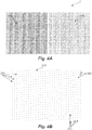
- Figure 4A shows a top plan view of an alternative version of the structured light generating substrate 2 of the apparatus 100 of Figure 1 comprising a first sector 25A and a second sector 25B having masks with similar geometrical patterns.
- Figure 4B shows an enlarged particular of the first sector 25A, wherein it can be seen that the substrate 2 has a coating 260 opaque to light, optionally made of chromium-based material (i.e., materials based on chromium oxide (Cr 2 O 3 ) or based on a mixture of Cr 2 O 3 and other species as chromium (Cr) and silicon dioxide (SiO 2 )), on which a plurality of circular holes 250, through which light can pass, are made by photolithography.
- chromium-based material i.e., materials based on chromium oxide (Cr 2 O 3 ) or based on a mixture of Cr 2 O 3 and other species as chromium (Cr) and silicon dioxide (SiO 2 )
- the plurality of circular holes 250 (the diameter of which is optionally ranging from 10 micrometers to 30 micrometers) is arranged according to a matrix pattern, wherein the circular holes are optionally disposed at the vertices of contiguous equal parallelograms, more optionally rhombuses, still more optionally square ones, whereby each circular hole 250 is spaced from the closest four circular holes 250 by the same distance (optionally ranging from 50 micrometers to 300 micrometers).
- the diameter of each circular hole and/or its distance from the closest four circular holes in one of the two sectors are different from the diameter of each circular hole and from its distance from the closest four circular holes, respectively, in the other sector; for instance, in the structured light generating substrate 2 of Figure 4A , the diameter of each circular hole 250 and its distance from the closest four circular holes 250 of the first sector 25A are greater than the diameter of each circular hole and its distance from the closest four circular holes, respectively, of the second sector 25B.
- the structured light generating substrate 2 may comprise a number of sectors, each provided with a respective plurality of circular holes arranged according to a matrix pattern, different from two, for instance one, or four, or a number of sectors equal to a power of 2; each sector has respective geometrical features of the pattern, and the limit on the area of the single sector is given by the desired area of the acquired image.
- the number of sectors and the geometrical features of the related patterns affects the mode of image acquisition, that is the scan (the necessary shifts) of the substrate 2 on the plane orthogonal to the optical axis.
- the microlens array 13 of Figure 2 may be provided, on its face directed towards the first relay lens 4a (i.e.
- the structured light beam is focused on the focal plane 3a of Figure 2 according to parallel lines similar to the geometrical pattern of Figures 3A and 3B or according to circular spots similar to the geometrical pattern of Figures 4A and 4B .
- the substrate of the array 13 may have, on the planar face opposite to the one directed towards the first relay lens 4a (i.e. on the planar face receiving the basic light beam), a coating opaque to light, optionally made of chromium-based material, subject to photolithography according to a geometrical pattern such that the coating is missing in correspondence with the microlenses, whereby such coating opaque to light is similar to the coating 210 of Figures 3A and 3B when the microlenses are generally cylindrical microlenses, or similar to the coating 260 of Figures 4A and 4B when the microlenses are generally hemispherical microlenses; however, it must be noted that such coating of the substrate of the array 13 is not an essential feature and may be also not present.
- Figure 5 shows a cross-section view of a portion of the array 13 of microlenses of Figure 2 in correspondence of a generally cylindrical microlens 596; however, it must be noted that, also when the array 13 of microlenses of Figure 2 is provided with generally hemispherical microlenses, the cross-section view in correspondence of a microlens is similar (if not exactly equal) to the one shown in Figure 5 .
- the array 13 of microlenses includes a substrate 590 having, on the planar face opposite to the one directed towards the first relay lens 4a (i.e. on the planar face receiving the basic light beam), a coating 592 subject to photolithography opaque to light, that is not present in correspondence with the generally cylindrical microlenses, one of which, indicated with the reference numeral 596, is shown in Figure 5 , with which the face of the substrate 590 directed towards the first relay lens 4a (i.e. the planar face focusing the structured light beam on the focal plane 3a shown in Figure 2 ) is provided.
- each generally cylindrical microlenses 596 are disposed such that each generally cylindrical microlens 596 is optically aligned with a corresponding continuous linear aperture 576 made in the coating 592 subject to photolithography opaque to light (as well as the generally hemispherical microlenses are disposed such that each generally hemispherical microlens is optically aligned with a corresponding circular aperture made in the coating subject to photolithography opaque to light).
- each generally cylindrical microlens 596 is positioned directly across the thickness of the array 13 in correspondence of a continuous linear aperture 576 of the coating 592.
- any light transmitted through a given continuous linear aperture 576 of the coating 592 passes through a corresponding generally cylindrical microlens 596, that focuses the same on the focal plane 3a shown in Figure 2 .
- each generally cylindrical microlens 596 (as well as each generally hemispherical microlens) of the array 13 has a generally semi-circular cross-section.
- the term "generally semi-circular” is taken to mean that the curvature of the outer surface of the generally cylindrical microlens 596 (as well as of a generally hemispherical microlens) of the array 13 needs not in all embodiments of the apparatus according to the invention to exactly correspond to the curve of a circle. Instead, the curvature of the generally cylindrical microlens 596 (as well as of a generally hemispherical microlens) may have an eccentricity different from an exact circle.
- the curvature of the generally cylindrical microlens 596 may be elliptical, parabolic, hyperbolic or even aspherical (i.e. corresponding to a conical surface with variable curvature radii).
- the term "generally semi-circular" encompasses all such embodiments.
- the microlenses of the array 13 may be composed of the same material as the substrate 590, and may be integrally formed on the same substrate 590, for instance during the same fabrication step. For example, they may be formed by a molding or etching process.
- confocal microscopy apparatus may comprise other structured light generating components different from the substrate 2 of Figure 1 and from the array 13 of microlenses of Figure 2 , such as for instance a digital micromirror device (DMD - Digital Micromirror Device), still remaining within the scope of protection of the invention.
- DMD digital micromirror device
- FIG 6A is a top plan view of an example of a spinning disk 7 according to some embodiments.
- the spinning disk 7 generally includes a central section 264 and an outer section 268 coaxially surrounding the central section 264.
- the central section 264 may be configured (e.g., as a hub) for attaching the spinning disk 7 to a shaft to enable motorized rotation of the spinning disk 7.
- the shaft may be attached to one side of the central section 264 and/or may pass through a central bore 270 of the spinning disk 7.
- the outer section 268 comprises an outer continuous slit annulus 272 and an inner continuous slit annulus 278 which also coaxially surround the central section 264.
- each one of the outer and inner annulii 272 and 278 has an inner radius and an outer radius, and spans a radial distance from the inner radius to the outer radius, whereby the outer radius of the inner annulus 278 is lower than the inner radius of the outer annulus 272; optionally, the radial distance of the inner annulus 278 is equal to the radial distance of the outer annulus 272.
- the outer and inner continuous slit annulii 272 and 278 may be, or be formed by, respective patterned masks as described further below.
- Each one of the outer and inner continuous slit annulii 272 and 278 includes a plurality of apertures 276 arranged along a plurality of spiral paths on the planar face of the spinning disk 7.
- the outer annulus 272 includes thirty-six spiral paths, while the inner annulus 278 includes twenty-four spiral paths; however, it must be noted that the number of the spiral paths is not an essential feature for the invention, and other variants of the spinning disk may include less or more than thirty-six and twenty-four spiral paths for continuous slit annulii.
- the spiral paths may be arranged adjacent to each other in a multi-start pattern, such that the spiral paths each start at a first radius of the spinning disk 7 (e.g., the inner radius of the outer annulus 272 and the inner radius of the inner annulus 278) and end at a second radius of the spinning disk 7 greater than the first radius (e.g., the outer radius of the outer annulus 272 and the outer radius of the inner annulus 278).
- the spiral paths may be non-Archimedean.
- the spinning disk 7 may include a number of continuous slit annulii different from two, for instance one or four or a different power of 2. Obviously, the number of sectors and the geometrical features of the related patterns affect the mode of image acquisition, that is the scan (the necessary shifts) of the spinning disk 7 on the plane orthogonal to the optical axis.
- each aperture 276 of the spinning disk 7 is a continuous spiral slit extending along a corresponding spiral path from the start to the end of that spiral path.
- Figure 6B shows an enlarged particular 372 of the outer continuous slit annulus 272 of the spinning disk 7 of Figure 6A .
- the apertures 276 are continuous spiral slits. Adjacent apertures 276 are spaced from each other by a separation distance (or “step” or “pitch") indicated as 380 in Figure 6B .
- the separation distance 380 ranges from 100 micrometers to 2 millimeters, more optionally from 100 micrometers to 1 millimeter.
- the separation distance 380 is constant over the entire extent of the spiral paths taken by the apertures 276, while in other embodiments the separation distance 380 may vary.
- the width of each spiral aperture 276 (the distance between opposing spiral edges of the aperture 276, i.e., the dimension transverse to the aperture 276) is of the order of micrometers, optionally ranging from 10 micrometers to 100 micrometers, more optionally from 20 micrometers to 70 micrometers.
- the separation distance and/or the dimensions of the width of the continuous spiral apertures of one of the two outer and inner annulii 272 and 278 are different from those of the other annulus; for instance, in the spinning disk 7 of Figure 6A , the separation distance 380 and the width of the continuous spiral apertures 276 of the outer annulus 272 are greater than those of the inner annulus 278.
- the width of the continuous spiral apertures is constant over the entire extent of the aperture, while in other embodiments the width may vary.
- the spinning disk 7 may include a number of annulii, each provided with respective continuous spiral slit apertures, different from two, for instance one, or four, or a number of sectors equal to a power of 2; each annulus has respective geometrical features of the continuous spiral slit apertures, in function of the desired area of the acquired image.
- the number of annulii and the geometrical features of the related patterns affect the mode of image acquisition, that is the scan (the necessary shifts) of the spinning disk 7 on the plane orthogonal to the optical axis.
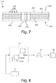
- FIG. 7 is a schematic cross-sectional view of a spinning disk 416 according to some other embodiments of the apparatus according to the invention.
- the spinning disk 416 may include a planar first side 456, an opposing planar second side 460, and a central bore 470.
- the thickness of the spinning disk 416 is defined between the first side 456 and the second side 460.
- the spinning disk 416 may further include a disk-shaped substrate 490 largely dictating the overall dimensions of the spinning disk 416, and a patterned mask 492.
- the substrate 490 includes a planar first surface and an opposing planar second surface corresponding to the first side 456 and the second side 460, respectively.
- the thickness of the substrate 490 extends from the first surface to the second surface along a direction orthogonal to the first surface and second surface. In some embodiments, the thickness of the substrate 490 is in a range from 0,5 mm to 2 mm.
- the substrate 490 may be composed of any optically transparent material suitable for use in a confocal microscope. Examples of materials for the substrate 490 include, but are not limited to, various glasses and quartz (including fused quartz), as well as certain optically transparent polymers.
- One non-limiting example of glass is borosilicate glass, such as BOROFLOAT® glasses available from SCHOTT North America, Inc., Louisville, Kentucky, USA.
- the substrate 490 may include a central section 464 that is distinct from the substrate 490 and may be composed of a different material.
- the patterned mask 492 includes a spiral pattern or arrangement of apertures 476 as described for the spinning disk 7 shown in Figures 6A and 6B .
- the patterned mask 492 is disposed on either the first surface or the second surface of the substrate 490.
- the patterned mask 492 may be composed of a suitable optically black (low-reflective) material.
- black materials include, but are not limited to, chrome-based materials, i.e., materials based on chromium oxide (Cr 2 O 3 ) or based on a mixture of Cr 2 O 3 and other species such as chromium (Cr) and silicon dioxide (SiO 2 ), a few examples being black chrome and blue chrome.
- the patterned mask 492 may be composed of a material that may be characterized as being a highly optically black (or, more simply, "highly black") material.
- a highly black material may have a hemispherical reflectance of less than 5% for the wavelength spectrum contemplated by the present disclosure (e.g., from about 350 to 750 nm).
- a highly black material may have a hemispherical reflectance of less than 2% for the wavelength spectrum.
- the highly black material of the patterned mask 492 may be a microstructured material or a material with a microstructured outer surface or coating.
- the microstructured material may have a dendritic finish such as a coating comprising closely spaced black peaks and/or ridges.
- the microstructured feature of the dendritic finish may consist of vertically-oriented, single-walled or multi-walled carbon nanotubes (CNTs).
- hemispherical reflectance or “total hemispherical reflectance” is the reflectance measured of all light that is scattered off of a test sample at all angles. This reflectance measurement may be performed according to known techniques. For example, hemispherical reflectance may be measured using an integrating sphere, in which an incoming light beam illuminates a test sample attached onto the sphere from a given direction and the radiation scattered by the sample is collected and detected, as disclosed by Quijada et al., Hemispherical Reflectance and Emittance Properties of Carbon Nanotubes Coatings at Infrared Wavelengths, CRYOGENIC OPTICAL SYSTEMS AND INSTRUMENTS XIII, Conference on Cryogenic Optical Systems and Instruments XIII, Vol. 8150, DOI: 10.1117/12.894601, p. 11 (2011 ).
- the patterned mask 492 is a thin layer (or film, coating, etc.) having a thickness of the order of micrometers.
- patterned mask 492 may have a thickness in a range from 0,1 micrometers to 0,3 micrometers.
- the patterned mask 492 may be fabricated by any technique suitable for its composition and thickness.
- the patterned mask 492 may be prefabricated and then laminated on the substrate 490.
- the patterned mask 492 may be formed on the substrate 490 by a microfabrication process such as, for example, electroplating, vacuum deposition (chemical vapor deposition or CVD, physical vapor deposition or PVD, etc.), evaporation, or by a wet coating technique (e.g., spray coating, dip coating, spin-on coating, etc.).
- the patterned mask 492 may be formed by first depositing a continuous layer and thereafter patterning the layer to form the apertures 476 by any suitable technique such as photolithography (e.g., masking and etching).
- the spinning disk 416 may include an anti-reflective layer or coating 494 that conformally coats (covers) the first side 456 and the second side 460.
- the anti-reflective layer 494 may be any material or multilayer stack of materials exhibiting effective anti-reflective characteristics for the spectrum of wavelengths contemplated by the present disclosure (e.g., from 350 nm to 700 nm, or about 350 nm to about 700 nm).
- the anti-reflective layer 494 is a high-performance anti-reflective layer.
- a high-performance anti-reflective layer is a material having an average reflectance (Rav) of less than or equal to 0,3% (Rav ⁇ 0,3%) over a wavelength range of 380 nm to 710 nm, and a maximum reflectance (Rmx) of less than or equal to 1% (Rmx ⁇ 1%) over the wavelength range of 380 nm to 710 nm.
- the high-performance anti-reflective layer may comprise one of (or a combination of two or more of) the fluoride materials and/or oxide materials noted above.
- the anti-reflective layer 494 is a thin layer (of the order of micrometers) applied by a vacuum deposition process.
- the anti-reflective layer 494 may be formed by applying the anti-reflective material to the substrate 490, followed by forming the patterned mask 492, followed by again applying the anti-reflective material so as to conformally coat the patterned mask 492.
- the patterned mask 492 is embedded in the anti-reflective coating 494, as illustrated in Figure 7 .
- the patterned mask 492 may first be formed directly on the substrate 490, followed by applying the anti-reflective coating 494 so as to conformally cover the patterned mask 492 and exposed surfaces of the substrate 490.
- the processing portion of the apparatus of Figure 1 comprises a processing central unit 16 receiving from the acquisition sensor 11 the set of the acquired N sub-frames 700A, 700B, ..., 700N of the plane of the sample 10; during acquisition, each sub-frame is advantageously stored in a memory 70, and the structured light generating component and the spinning disk 7 are moved to illuminate with the structured light beam another portion of the plane of the sample 10 thus acquiring the next sub-frame.
- next sub-frames continues up to the coverage of the entire plane of the sample 10, and then the sub-frames are combined into a super-resolved final image 80 of the plane under examination thanks to the processing performed by the central unit 16 by using structured light microscopy deconvolution algorithms, such as for instance those disclosed in document WO2013144891 or those disclosed by R. Heintzmann in Structured illumination methods, in Handbook of Biological Confocal microscopy, chapter 13, J.B. Pawley editor, New York, 2006 .
- structured light microscopy deconvolution algorithms such as for instance those disclosed in document WO2013144891 or those disclosed by R. Heintzmann in Structured illumination methods, in Handbook of Biological Confocal microscopy, chapter 13, J.B. Pawley editor, New York, 2006 .
- the central unit 16 comprises one or more graphics processors or GPUs (Graphics Processing Unit), optionally a CUDA (Compute Unified Device Architecture) unit available from the US company Nvidia Corporation, so as to exploit the parallel computing, one or more volatile and non-volatile memories for storing data, one or more data input devices (e.g. keyboard, touch screen, mouse), one or more user/processor interface devices (e.g. monitor).
- graphics processors or GPUs Graphics Processing Unit
- CUDA Computer Unified Device Architecture
- the central unit 16 also controls the operation of all the components of the confocal microscopy apparatus 100 according to the invention, in particular the automated moving units (e.g. motorised devices) allowing the structured light generating component (i.e., the substrate 2 or the microlens array 13) to be moved with movements in the plane perpendicular to the optical axis, in order to acquire an image of an entire plane of the sample 10.
- the central unit 16 also controls the automated units for moving the spinning disk 7 that is rotated.
- the acquisition portion of the confocal microscopy apparatus may be fabricated and marketed independently from the processing portion; also, the acquisition portion of the confocal microscopy apparatus may be fabricated and marketed independently from the presence of the light source (indicated with the reference numeral 1 in Figures 1 and 2 ), that could be mounted afterwards in correspondence of a related housing configured to house a light source, and/or of the acquisition sensor (indicated with the reference numeral 11 in Figures 1 and 2 ), that could be mounted afterwards in correspondence of a related housing configured to house an acquisition sensor.
- the light source indicated with the reference numeral 1 in Figures 1 and 2
- the acquisition sensor indicated with the reference numeral 11 in Figures 1 and 2
- the acquisition portion could be also provided with an electronic unit for controlling the operation of the components of the same acquisition portion, in particular the automated moving units (e.g. motorised devices) allowing the structured light generating component (i.e., the substrate 2 or the microlens array 13) to be moved with movements in the plane perpendicular to the optical axis, and the automated units for moving the spinning disk 7 that is rotated;
- the automated moving units e.g. motorised devices
- the structured light generating component i.e., the substrate 2 or the microlens array 13
- the automated units for moving the spinning disk 7 that is rotated such controlling electronic unit is configured to be connected with an external central unit processing the images acquired by the acquisition sensor, possibly an acquisition sensor external to the acquisition portion.
- the acquisition of the set of sub-frames of the entire plane of the sample occurs by rotating the spinning disk 7 in the excitation and emission optical path, while the structured light generating component (i.e. the substrate 2 or the microlens array 13) is arranged in the excitation optical path and moved in the plane perpendicular to the optical axis, while the focal plane 3a of the structured light beam, the focal plane 3b of the excitation beam, and the plane of which the images of the sample 10 are to be acquired are optically conjugated to the focal plane of the acquisition sensor 11.
- the structured light generating component i.e. the substrate 2 or the microlens array 13
Landscapes
- Physics & Mathematics (AREA)
- General Physics & Mathematics (AREA)
- Chemical & Material Sciences (AREA)
- Analytical Chemistry (AREA)
- Optics & Photonics (AREA)
- Engineering & Computer Science (AREA)
- Theoretical Computer Science (AREA)
- Multimedia (AREA)
- Microscoopes, Condenser (AREA)
Claims (15)
- Konfokalmikroskopiegerät (100; 200), das Folgendes umfasst:- eine strukturierte lichterzeugende Komponente (2; 13), die so konfiguriert ist, dass sie mit einem Basis-Lichtstrahl beleuchtet wird und einen auf eine erste Ebene (3a) fokussierten strukturierten Lichtstrahl erzeugt;- eine sich drehende Scheibe (7), die so konfiguriert ist, dass sie den strukturierten Lichtstrahl empfängt und einen resultierenden Anregungsstrahl zu einer Optik (8, 9) eines Mikroskops (15) überträgt, die auf eine Ebene einer Probe (10) fokussiert ist, wobei die sich drehende Scheibe (7) auf einer zweiten Ebene (3b) liegt und ein scheibenförmiges Substrat (490) aus einem optisch transparenten Material umfasst, wobei das Substrat (490) der sich drehenden Scheibe (7) eine ebene erste Oberfläche (456) und eine gegenüberliegende ebene zweite Oberfläche (460) und eine strukturierte Maske (492) umfasst, die auf einer von der ersten Oberfläche (456) und der zweiten Oberfläche (460) angeordnet ist und mindestens einen Sektor umfasst, der mit einer oder mehreren kontinuierlichen spiralförmigen Schlitzöffnungen (476) versehen ist, wobei die strukturierte Maske (492) oder eine äußere Oberfläche davon aus einem hochschwarzen, für Licht undurchsichtigen Material besteht;- ein Gehäuse, das dazu ausgelegt ist, auf einer dritten Ebene (3c) einen Erfassungssensor (11) aufzunehmen, der dazu ausgelegt ist, einen von der Ebene der Probe (10) emittierten Fluoreszenzstrahl zu erfassen;- einen Satz von Zwischenlinsen (relay lens) (4a, 4b, 4c), die so konfiguriert sind, dass sie die erste Ebene (3a), die zweite Ebene (3b) und die Ebene der Probe (10) optisch mit der dritten Ebene (3c) konjugieren;- optische Mittel (5, 6), die so konfiguriert sind, dass sie den strukturierten Lichtstrahl von der strukturierten lichterzeugenden Komponente (2; 13) zu der Ebene der Probe (10) und den emittierten Fluoreszenzstrahl von der Ebene der Probe (10) zu dem Gehäuse übertragen, das zur Aufnahme des Erfassungssensors (11) konfiguriert ist; und- Bewegungsmittel, die so konfiguriert sind, dass sie die strukturierte lichterzeugende Komponente (2; 13) so bewegen, dass der strukturierte Lichtstrahl in der ersten Ebene (3a) verschoben wird, und die rotierende Scheibe (7) in der zweiten Ebene (3b) bewegen.
- Vorrichtung (100) nach Anspruch 1, wobei die strukturierte lichterzeugende Komponente ein strukturiertes Lichterzeugungs-Substrat (2) umfasst, das mit mindestens einem Sektor (20A, 20B; 25A, 25B) versehen ist, der eine Maske (210; 260) aus einem lichtundurchlässigen Material gemäß einem geometrischen Muster aufweist, das mit einer Vielzahl von Öffnungen (200; 250) aus optisch transparentem Material versehen ist, die so konfiguriert sind, dass sie den BasisLichtstrahl durchlassen, um einen strukturierten Lichtstrahl zu erhalten, wobei die erste Ebene (3a) die Ebene ist, auf der das strukturierte lichterzeugende Substrat (2) liegt.
- Vorrichtung (100) nach Anspruch 2, wobei das strukturierte Lichterzeugungs-Substrat (2) aus dem optisch transparenten Material, optional aus Glas, hergestellt ist, das eine lichtundurchlässige Beschichtung (210) aufweist, die optional aus einem Material auf Chrombasis hergestellt ist und mit den Öffnungen (200; 250) versehen ist, die optional durch Photolithographie hergestellt sind.
- Vorrichtung (100) nach Anspruch 2 oder 3, wobei die genannten Öffnungen aus der Gruppe ausgewählt sind, die Folgendes umfasst:- parallele lineare Öffnungen (200) mit einer optionalen Breite im Bereich von 10 Mikrometern bis 30 Mikrometern und einem gegenseitigen Abstand im Bereich von 50 Mikrometern bis 300 Mikrometern, und- kreisförmige Löcher (250) mit einem optionalen Durchmesser im Bereich von 10 Mikrometern bis 30 Mikrometern, die gemäß einem Matrixmuster angeordnet sind, wobei die kreisförmigen Löcher (250) optional an den Ecken von aneinandergrenzenden gleichen Parallelogrammen, optional Rhomben, optional Quadraten angeordnet sind, wobei jedes kreisförmige Loch (250) von den vier nächstgelegenen kreisförmigen Löchern (250) um einen gleichen Abstand, optional im Bereich von 50 Mikrometern bis 300 Mikrometern, beabstandet ist.
- Vorrichtung (200) nach Anspruch 1, wobei die strukturiertes Licht erzeugende Komponente eine Anordnung (13) von strukturiertes Licht erzeugenden Mikrolinsen (596) umfasst, die ein Substrat (590) umfasst, das auf einer Fläche mit einer Vielzahl von Mikrolinsen (596) versehen ist, die so konfiguriert sind, dass sie den strukturierten Lichtstrahl erzeugen, der auf eine Brennebene (3a) fokussiert ist.
- Vorrichtung (200) nach Anspruch 5, wobei die Mikrolinsen (596) aus der Gruppe ausgewählt sind, die Folgendes umfasst:- im Allgemeinen zylindrische lineare Mikrolinsen, die so konfiguriert sind, dass sie den strukturierten Lichtstrahl gemäß parallelen Linien auf die Brennebene (3a) fokussieren, wobei die parallelen Linien eine Breite haben, die optional in einem Bereich von 10 Mikrometer bis 30 Mikrometer liegt, und einen gegenseitigen Abstand, der optional in einem Bereich von 50 Mikrometer bis 300 Mikrometer liegt, und- im Allgemeinen halbkreisförmige Mikrolinsen, die so konfiguriert sind, dass sie den strukturierten Lichtstrahl auf die Brennebene (3a) gemäß kreisförmigen Punkten fokussieren, die gemäß einem Matrixmuster angeordnet sind, wobei die kreisförmigen Punkte einen Durchmesser aufweisen, der optional in einem Bereich von 10 Mikrometer bis 30 Mikrometer liegt, und optional an den Ecken von benachbarten gleichen Parallelogrammen, mehr optional Rhomben, noch mehr optional Quadraten angeordnet sind, wobei jeder kreisförmige Punkt von den nächstgelegenen vier kreisförmigen Punkten (250) um einen gleichen Abstand beabstandet ist, der optional in einem Bereich von 50 Mikrometer bis 300 Mikrometer liegt.
- Vorrichtung (200) nach Anspruch 5 oder 6, wobei das Substrat (590) der Anordnung (13) von Mikrolinsen (596) mit einer lichtdurchlässigen Beschichtung (592) versehen ist, die optional aus einem Material auf Chrombasis hergestellt ist und einer Photolithographie gemäß einem geometrischen Muster unterzogen wurde, so dass die Beschichtung (592) in Übereinstimmung mit den Mikrolinsen (596) fehlt, wobei jede Mikrolinse (596) optisch mit einer entsprechenden, in der Beschichtung (592) hergestellten Öffnung (576) ausgerichtet ist.
- Vorrichtung (100) nach Anspruch 1, wobei die strukturierte lichterzeugende Komponente eine digitale Mikrospiegelvorrichtung umfasst.
- Vorrichtung (100; 200) nach einem der vorhergehenden Ansprüche, wobei der Satz von Zwischenlinsen eine erste Zwischenlinse (4a), eine zweite Zwischenlinse (4b) und eine dritte Zwischenlinse (4c) umfasst und die optischen Mittel (5; 6) einen dichroitischen Filter (5) umfassen, wobei die erste Zwischenlinse (4a) so konfiguriert ist, dass sie von dem strukturierten Lichtstrahl durchquert wird, der dichroitische Filter (5) so konfiguriert ist, dass er den von der ersten Zwischenlinse (4a) kommenden strukturierten Lichtstrahl in Richtung der zweiten Zwischenlinse (4b) reflektiert, die so konfiguriert ist, dass sie den strukturierten Lichtstrahl auf die sich drehende Scheibe (7) fokussiert, wobei der dichroitische Filter (5) ferner so konfiguriert ist, dass er den von der sich drehenden Scheibe (7) kommenden emittierten Fluoreszenzstrahl in Richtung des Gehäuses durchlässt, das so konfiguriert ist, dass es den Erfassungssensor (11) aufnimmt.
- Vorrichtung (100; 200) nach Anspruch 9, wobei das optische Mittel (5; 6) ferner einen Emissionsfilter (6) umfasst, der zwischen dem dichroitischen Filter (5) und dem Gehäuse angeordnet ist, das zur Aufnahme des Erfassungssensors (11) konfiguriert ist, wobei der Emissionsfilter (6) so konfiguriert ist, dass er den emittierten Fluoreszenzstrahl, der von dem dichroitischen Filter (5) kommt, selektiv in Richtung des zur Aufnahme des Erfassungssensors (11) konfigurierten Gehäuses durchlässt.
- Vorrichtung (100; 200) nach Anspruch 10, wobei der Emissionsfilter (6) zwei oder mehr Abschnitte umfasst, von denen jeder so konfiguriert ist, dass er nur von einem entsprechenden Teil des emittierten Fluoreszenzstrahls mit einem entsprechenden Wellenlängenbereich durchquert wird.
- Vorrichtung (100; 200) nach Anspruch 11, wobei der Emissionsfilter (6) auf einem Wellenlängenselektor montiert ist, wobei der Wellenlängenselektor optional ein motorisiertes Rad und/oder mindestens eine piezoelektrische Vorrichtung und/oder mindestens eine motorisierte Vorrichtung umfasst.
- Vorrichtung (100; 200) nach einem der vorhergehenden Ansprüche, die außerdem Folgendes umfasst: eine Lichtquelle (1), die so konfiguriert ist, dass sie den Basis-Lichtstrahl emittiert;
einen Erfassungssensor (11), der in dem Gehäuse untergebracht und so konfiguriert ist, dass er einen von der Ebene der Probe (10) emittierten Fluoreszenzstrahl erfasst; und- eine Verarbeitungszentraleinheit (16), die so konfiguriert ist, dass sie von dem Erfassungssensor (11) eine Vielzahl von Teilerfassungen (700A, 700B, ..., 700N) der Ebene der Probe (10) empfängt und diese Vielzahl von Teilerfassungen (700A, 700B, ..., 700N) zu einem Endbild (80) der Ebene der Probe (10) durch Verarbeitung mit Dekonvolutionsalgorithmen der strukturierten Lichtmikroskopie kombiniert. - Vorrichtung (100; 200) nach Anspruch 13, wobei die Verarbeitungszentraleinheit (16) einen oder mehrere Grafikprozessoren oder GPUs umfasst.
- Verfahren zum Erfassen und Verarbeiten von Bildern in der Konfokalmikroskopie mit strukturierten Licht, umfassend die folgenden Schritte:A. Bewirken, dass eine sich drehende Scheibe (7) von einem strukturierten Lichtstrahl durchquert wird, um einen resultierenden Anregungslichtstrahl zu erhalten, wobei die sich drehende Scheibe (7) ein scheibenförmiges Substrat (490) aus einem optisch transparenten Material umfasst, wobei das Substrat (490) der sich drehenden Scheibe (7) eine ebene erste Oberfläche (456) und eine gegenüberliegende ebene zweite Oberfläche (460) und eine strukturierte Maske (492) umfasst, die auf der ersten Oberfläche (456) oder der zweiten Oberfläche (460) angeordnet ist und mindestens einen Sektor umfasst, der mit einer oder mehreren kontinuierlichen spiralförmigen Schlitzöffnungen (476) versehen ist, wobei die strukturierte Maske (492) oder eine äußere Oberfläche davon aus einem hochschwarzen, für Licht undurchlässigen Material besteht;B. Fokussieren des resultierenden Anregungsstrahls auf eine Ebene einer Probe (10);C. Erfassen einer Vielzahl von Teilerfassungen (700A, 700B, ..., 700N) der Ebene der Probe (10); undD. Kombinieren einer solchen Vielzahl von Teilerfassungen (700A, 700B, ..., 700N) zu einem endgültigen Bild (80) der genannten Ebene der Probe (10) durch Verarbeitung mit Dekonvolutionsalgorithmen der strukturierten Lichtmikroskopie.
Applications Claiming Priority (2)
| Application Number | Priority Date | Filing Date | Title |
|---|---|---|---|
| ITUB2015A004591A ITUB20154591A1 (it) | 2015-10-12 | 2015-10-12 | Apparato di microscopia confocale e relativo procedimento di acquisizione ed elaborazione di immagini |
| PCT/IB2016/056100 WO2017064629A1 (en) | 2015-10-12 | 2016-10-12 | Confocal microscopy apparatus and related process for acquiring and processing images |
Publications (2)
| Publication Number | Publication Date |
|---|---|
| EP3362836A1 EP3362836A1 (de) | 2018-08-22 |
| EP3362836B1 true EP3362836B1 (de) | 2020-06-03 |
Family
ID=55273355
Family Applications (1)
| Application Number | Title | Priority Date | Filing Date |
|---|---|---|---|
| EP16801303.5A Active EP3362836B1 (de) | 2015-10-12 | 2016-10-12 | Konfokale mikroskopievorrichtung und entsprechendes verfahren zur aufnahme und verarbeitung von bildern |
Country Status (4)
| Country | Link |
|---|---|
| US (1) | US20180292634A1 (de) |
| EP (1) | EP3362836B1 (de) |
| IT (1) | ITUB20154591A1 (de) |
| WO (1) | WO2017064629A1 (de) |
Cited By (2)
| Publication number | Priority date | Publication date | Assignee | Title |
|---|---|---|---|---|
| IT202300010944A1 (it) | 2023-05-30 | 2024-11-30 | Crestoptics S P A | Apparato di microscopia confocale |
| WO2025257638A1 (en) | 2024-06-10 | 2025-12-18 | Crestoptics S.P.A. | Confocal microscopy apparatus |
Families Citing this family (10)
| Publication number | Priority date | Publication date | Assignee | Title |
|---|---|---|---|---|
| US10501493B2 (en) | 2011-05-27 | 2019-12-10 | Rqx Pharmaceuticals, Inc. | Broad spectrum antibiotics |
| US10392422B2 (en) | 2014-05-20 | 2019-08-27 | Rqx Pharmaceuticals, Inc. | Macrocyclic broad spectrum antibiotics |
| RU2761476C2 (ru) | 2015-11-20 | 2021-12-08 | АрКьюИкс ФАРМАСЬЮТИКЭЛС, ИНК. | Макроциклические антибиотики широкого спектра действия |
| CN108227233B (zh) * | 2017-12-27 | 2020-02-21 | 清华大学 | 基于光片结构光的显微层析超分辨率成像方法及系统 |
| DE102018114162B4 (de) | 2018-06-13 | 2023-01-19 | Solarius Asia Ltd. | Lochscheibe zum Selektieren von Licht für eine optische Abbildung, optisches Abbildungssystem |
| KR102104238B1 (ko) * | 2018-10-19 | 2020-04-24 | 한국과학기술연구원 | 광변조기 기반 구조 조명 현미경 시스템 및 상기 시스템에 의해 수행되는 이미지 생성 방법 |
| DE102018128590A1 (de) * | 2018-11-14 | 2020-05-14 | Carl Zeiss Microscopy Gmbh | Fluktuationsbasierte Fluoreszenzmikroskopie |
| WO2020205952A1 (en) | 2019-04-02 | 2020-10-08 | Thermo Electron Scientific Instruments Llc | Enhanced sample imaging using structured illumination microscopy |
| PT3968983T (pt) | 2019-05-28 | 2023-10-04 | Hoffmann La Roche | Antibióticos macrocíclicos de largo espectro |
| CN115685571A (zh) * | 2022-11-11 | 2023-02-03 | 执鼎医疗科技(杭州)有限公司 | 图像纠偏机构及显像仪 |
Citations (1)
| Publication number | Priority date | Publication date | Assignee | Title |
|---|---|---|---|---|
| JPH1048530A (ja) * | 1996-08-08 | 1998-02-20 | Yokogawa Electric Corp | 共焦点光スキャナ |
Family Cites Families (31)
| Publication number | Priority date | Publication date | Assignee | Title |
|---|---|---|---|---|
| US5671085A (en) * | 1995-02-03 | 1997-09-23 | The Regents Of The University Of California | Method and apparatus for three-dimensional microscopy with enhanced depth resolution |
| US5760950A (en) * | 1996-07-25 | 1998-06-02 | Advanced Scanning, Ltd. | Scanning confocal microscope |
| US6219461B1 (en) * | 1997-07-29 | 2001-04-17 | Cognex Corporation | Determining a depth |
| ATE272224T1 (de) * | 1997-11-17 | 2004-08-15 | Max Planck Gesellschaft | Konfokales spektroskopiesystem und -verfahren |
| DE19918689C2 (de) * | 1999-04-23 | 2003-05-28 | Rudolf Groskopf | Vorrichtung zur dreidimensionalen konfocalen optischen Untersuchung eines Objektes mit Beleuchtung durch eine Lochplatte |
| US20070025504A1 (en) * | 2003-06-20 | 2007-02-01 | Tumer Tumay O | System for molecular imaging |
| US20060087727A1 (en) * | 2004-10-21 | 2006-04-27 | Jeffrey Brooker | Apparatus, system and method for selective photobleaching, imaging and confocal microscopy |
| US8362431B2 (en) * | 2005-03-15 | 2013-01-29 | Mount Holyoke College | Methods of thermoreflectance thermography |
| US7839496B2 (en) * | 2008-04-24 | 2010-11-23 | Araca Incorporated | Confocal microscopy pad sample holder and method of hand using the same |
| JP4596284B2 (ja) * | 2008-05-26 | 2010-12-08 | ソニー株式会社 | 光ディスク装置及びフォーカス制御方法 |
| GB0900526D0 (en) * | 2009-01-14 | 2009-02-11 | Perkinelmer Ltd | Fluorescence microscopy methods and apparatus |
| US7869027B2 (en) * | 2009-04-20 | 2011-01-11 | Araca, Inc. | Confocal microscopy pad sample holder that measures displacement and method of using the same |
| JP5371694B2 (ja) * | 2009-10-26 | 2013-12-18 | オリンパス株式会社 | 顕微鏡接続ユニットおよび顕微鏡システム |
| GB201019181D0 (en) * | 2010-11-12 | 2010-12-29 | Univ Leicester | Improved optical arrangement |
| DE102011114500B4 (de) * | 2011-09-29 | 2022-05-05 | Fei Company | Mikroskopvorrichtung |
| JP5527625B2 (ja) * | 2011-11-22 | 2014-06-18 | 横河電機株式会社 | 顕微鏡装置 |
| JP6140737B2 (ja) * | 2012-02-23 | 2017-05-31 | ザ ユナイテッド ステイツ オブ アメリカ, アズ リプレゼンテッド バイ ザ セクレタリー, デパートメント オブ ヘルス アンド ヒューマン サービシーズ | 多焦点構造化照射顕微鏡検査システムおよび方法 |
| US9047660B2 (en) * | 2012-03-01 | 2015-06-02 | Siemens Corporation | Network cycle features in relative neighborhood graphs |
| ITPI20120034A1 (it) * | 2012-03-31 | 2013-10-01 | Cnr Consiglio Naz Delle Ricer Che | Metodo e dispositivo perfezionati per microscopia video-confocale |
| DE102012007045B4 (de) * | 2012-04-05 | 2023-03-16 | Carl Zeiss Microscopy Gmbh | Vorrichtung und Verfahren zur Mikroskopie |
| DE102012009836A1 (de) * | 2012-05-16 | 2013-11-21 | Carl Zeiss Microscopy Gmbh | Lichtmikroskop und Verfahren zur Bildaufnahme mit einem Lichtmikroskop |
| WO2014005195A2 (en) * | 2012-07-05 | 2014-01-09 | Martin Russell Harris | Structured illumination microscopy apparatus and method |
| EP2712542B1 (de) * | 2012-09-28 | 2017-04-12 | Ruprecht-Karls-Universität Heidelberg | Ophthalmoskop mit strukturierter Beleuchtung |
| EP2713195B1 (de) * | 2012-09-28 | 2017-04-12 | Universität Heidelberg | Hochauflösende Mikroskopie mittels strukturierter Beleuchtung bei großen Arbeitsdistanzen |
| WO2014070912A1 (en) * | 2012-10-30 | 2014-05-08 | Cohen Adam E | Spatial filter enhanced spinning disk confocal microscope |
| EP2733514B1 (de) * | 2012-11-16 | 2020-09-30 | PerkinElmer Cellular Technologies Germany GmbH | Mikroskopvorrichtung zur strukturierten Beleuchtung einer Probe |
| DE102013001238B4 (de) * | 2013-01-25 | 2020-06-10 | Carl Zeiss Microscopy Gmbh | Lichtmikroskop und Mikroskopieverfahren |
| DE102013218231A1 (de) * | 2013-09-11 | 2015-03-12 | Sirona Dental Systems Gmbh | Optisches System zur Erzeugung eines sich zeitlich ändernden Musters für ein Konfokalmikroskop |
| US10539772B2 (en) * | 2013-10-09 | 2020-01-21 | Howard Hughes Medical Institute | Multiview light-sheet microscopy |
| DE102014004249A1 (de) * | 2014-03-24 | 2015-09-24 | Carl Zeiss Microscopy Gmbh | Konfokales Mikroskop mit Aperturkorrelation |
| US10533942B2 (en) * | 2014-08-10 | 2020-01-14 | JianFeng Zhang | System and method for measuring oil content in water using laser-induced fluorescent imaging |
-
2015
- 2015-10-12 IT ITUB2015A004591A patent/ITUB20154591A1/it unknown
-
2016
- 2016-10-12 US US15/764,332 patent/US20180292634A1/en not_active Abandoned
- 2016-10-12 WO PCT/IB2016/056100 patent/WO2017064629A1/en not_active Ceased
- 2016-10-12 EP EP16801303.5A patent/EP3362836B1/de active Active
Patent Citations (1)
| Publication number | Priority date | Publication date | Assignee | Title |
|---|---|---|---|---|
| JPH1048530A (ja) * | 1996-08-08 | 1998-02-20 | Yokogawa Electric Corp | 共焦点光スキャナ |
Cited By (3)
| Publication number | Priority date | Publication date | Assignee | Title |
|---|---|---|---|---|
| IT202300010944A1 (it) | 2023-05-30 | 2024-11-30 | Crestoptics S P A | Apparato di microscopia confocale |
| WO2024246684A1 (en) * | 2023-05-30 | 2024-12-05 | Crestoptics S.P.A. | Confocal microscopy apparatus |
| WO2025257638A1 (en) | 2024-06-10 | 2025-12-18 | Crestoptics S.P.A. | Confocal microscopy apparatus |
Also Published As
| Publication number | Publication date |
|---|---|
| WO2017064629A1 (en) | 2017-04-20 |
| US20180292634A1 (en) | 2018-10-11 |
| EP3362836A1 (de) | 2018-08-22 |
| ITUB20154591A1 (it) | 2017-04-12 |
Similar Documents
| Publication | Publication Date | Title |
|---|---|---|
| US20180292634A1 (en) | Confocal microscopy apparatus and related process for acquiring and processing images | |
| JP7126885B2 (ja) | 回折バイオセンサ | |
| KR101683408B1 (ko) | 분광 측정 장치 | |
| JP5120873B2 (ja) | 分光計測装置及び分光計測方法 | |
| EP2898312B1 (de) | Verfahren zur auflösung von positionen in der stochastischen fluoreszenz mikroskopie mit dreidimensionaler strukturierter beleuchtung | |
| CN104956249B (zh) | 光学显微镜和显微术方法 | |
| WO2020077780A1 (zh) | 共聚焦三维测量装置及其多孔径尼普科夫圆盘 | |
| JP2013511041A (ja) | 減衰全反射に基づいた光センサシステムおよび感知方法 | |
| JP7481351B2 (ja) | 波面解析装置、蛍光顕微鏡画像化システムおよび対象を顕微鏡画像化する方法 | |
| JP2002530668A (ja) | Sprセンサの並列読出しのための測定集成装置 | |
| EP3458896B1 (de) | Mikrolokalisierungsverfahren und mikrolokalisierungsvorrichtung für bildgebungsinstrument und eine messvorrichtung | |
| EP4334674A1 (de) | Systeme und verfahren zur erfassung dreidimensionaler bilder unter verwendung spektraler informationen | |
| US9229213B2 (en) | Coincident focus microscope having superior resolution and contrast in three dimensions | |
| US9476827B2 (en) | System and method of multitechnique imaging for the chemical biological or biochemical analysis of a sample | |
| Olevsko et al. | A colour-encoded nanometric ruler for axial super-resolution microscopies | |
| US20250283169A1 (en) | Enhanced resolution imaging | |
| WO2013064843A1 (en) | Support for microscope sample comprising a diffraction grating for forming an illumination pattern thereon | |
| CN119110913A (zh) | 光源阵列、傅里叶层叠成像的成像系统以及执行傅里叶层叠成像术的方法 | |
| CN115452735A (zh) | 一种超微区域光谱测试系统及方法 | |
| US10908404B2 (en) | Patterned optic for epi-fluorescence collection | |
| KR101167071B1 (ko) | 닙코우 디스크의 핀홀 배치 방법 | |
| CN218157548U (zh) | 结构化照明显微术系统 | |
| JP2014115592A (ja) | 観察装置、観察方法、及び光学部材 | |
| Skinner-Ramos | Toward phase-imaging optical nanoscopes |
Legal Events
| Date | Code | Title | Description |
|---|---|---|---|
| STAA | Information on the status of an ep patent application or granted ep patent |
Free format text: STATUS: UNKNOWN |
|
| STAA | Information on the status of an ep patent application or granted ep patent |
Free format text: STATUS: THE INTERNATIONAL PUBLICATION HAS BEEN MADE |
|
| PUAI | Public reference made under article 153(3) epc to a published international application that has entered the european phase |
Free format text: ORIGINAL CODE: 0009012 |
|
| STAA | Information on the status of an ep patent application or granted ep patent |
Free format text: STATUS: REQUEST FOR EXAMINATION WAS MADE |
|
| 17P | Request for examination filed |
Effective date: 20180510 |
|
| AK | Designated contracting states |
Kind code of ref document: A1 Designated state(s): AL AT BE BG CH CY CZ DE DK EE ES FI FR GB GR HR HU IE IS IT LI LT LU LV MC MK MT NL NO PL PT RO RS SE SI SK SM TR |
|
| AX | Request for extension of the european patent |
Extension state: BA ME |
|
| DAV | Request for validation of the european patent (deleted) | ||
| DAX | Request for extension of the european patent (deleted) | ||
| GRAP | Despatch of communication of intention to grant a patent |
Free format text: ORIGINAL CODE: EPIDOSNIGR1 |
|
| STAA | Information on the status of an ep patent application or granted ep patent |
Free format text: STATUS: GRANT OF PATENT IS INTENDED |
|
| INTG | Intention to grant announced |
Effective date: 20200109 |
|
| GRAS | Grant fee paid |
Free format text: ORIGINAL CODE: EPIDOSNIGR3 |
|
| GRAA | (expected) grant |
Free format text: ORIGINAL CODE: 0009210 |
|
| STAA | Information on the status of an ep patent application or granted ep patent |
Free format text: STATUS: THE PATENT HAS BEEN GRANTED |
|
| AK | Designated contracting states |
Kind code of ref document: B1 Designated state(s): AL AT BE BG CH CY CZ DE DK EE ES FI FR GB GR HR HU IE IS IT LI LT LU LV MC MK MT NL NO PL PT RO RS SE SI SK SM TR |
|
| REG | Reference to a national code |
Ref country code: GB Ref legal event code: FG4D |
|
| REG | Reference to a national code |
Ref country code: CH Ref legal event code: EP Ref country code: AT Ref legal event code: REF Ref document number: 1277599 Country of ref document: AT Kind code of ref document: T Effective date: 20200615 |
|
| REG | Reference to a national code |
Ref country code: DE Ref legal event code: R096 Ref document number: 602016037619 Country of ref document: DE |
|
| REG | Reference to a national code |
Ref country code: LT Ref legal event code: MG4D |
|
| PG25 | Lapsed in a contracting state [announced via postgrant information from national office to epo] |
Ref country code: GR Free format text: LAPSE BECAUSE OF FAILURE TO SUBMIT A TRANSLATION OF THE DESCRIPTION OR TO PAY THE FEE WITHIN THE PRESCRIBED TIME-LIMIT Effective date: 20200904 Ref country code: LT Free format text: LAPSE BECAUSE OF FAILURE TO SUBMIT A TRANSLATION OF THE DESCRIPTION OR TO PAY THE FEE WITHIN THE PRESCRIBED TIME-LIMIT Effective date: 20200603 Ref country code: NO Free format text: LAPSE BECAUSE OF FAILURE TO SUBMIT A TRANSLATION OF THE DESCRIPTION OR TO PAY THE FEE WITHIN THE PRESCRIBED TIME-LIMIT Effective date: 20200903 Ref country code: SE Free format text: LAPSE BECAUSE OF FAILURE TO SUBMIT A TRANSLATION OF THE DESCRIPTION OR TO PAY THE FEE WITHIN THE PRESCRIBED TIME-LIMIT Effective date: 20200603 Ref country code: FI Free format text: LAPSE BECAUSE OF FAILURE TO SUBMIT A TRANSLATION OF THE DESCRIPTION OR TO PAY THE FEE WITHIN THE PRESCRIBED TIME-LIMIT Effective date: 20200603 |
|
| REG | Reference to a national code |
Ref country code: NL Ref legal event code: MP Effective date: 20200603 |
|
| PG25 | Lapsed in a contracting state [announced via postgrant information from national office to epo] |
Ref country code: RS Free format text: LAPSE BECAUSE OF FAILURE TO SUBMIT A TRANSLATION OF THE DESCRIPTION OR TO PAY THE FEE WITHIN THE PRESCRIBED TIME-LIMIT Effective date: 20200603 Ref country code: HR Free format text: LAPSE BECAUSE OF FAILURE TO SUBMIT A TRANSLATION OF THE DESCRIPTION OR TO PAY THE FEE WITHIN THE PRESCRIBED TIME-LIMIT Effective date: 20200603 Ref country code: LV Free format text: LAPSE BECAUSE OF FAILURE TO SUBMIT A TRANSLATION OF THE DESCRIPTION OR TO PAY THE FEE WITHIN THE PRESCRIBED TIME-LIMIT Effective date: 20200603 Ref country code: BG Free format text: LAPSE BECAUSE OF FAILURE TO SUBMIT A TRANSLATION OF THE DESCRIPTION OR TO PAY THE FEE WITHIN THE PRESCRIBED TIME-LIMIT Effective date: 20200903 |
|
| REG | Reference to a national code |
Ref country code: AT Ref legal event code: MK05 Ref document number: 1277599 Country of ref document: AT Kind code of ref document: T Effective date: 20200603 |
|
| PG25 | Lapsed in a contracting state [announced via postgrant information from national office to epo] |
Ref country code: AL Free format text: LAPSE BECAUSE OF FAILURE TO SUBMIT A TRANSLATION OF THE DESCRIPTION OR TO PAY THE FEE WITHIN THE PRESCRIBED TIME-LIMIT Effective date: 20200603 Ref country code: NL Free format text: LAPSE BECAUSE OF FAILURE TO SUBMIT A TRANSLATION OF THE DESCRIPTION OR TO PAY THE FEE WITHIN THE PRESCRIBED TIME-LIMIT Effective date: 20200603 |
|
| PG25 | Lapsed in a contracting state [announced via postgrant information from national office to epo] |
Ref country code: EE Free format text: LAPSE BECAUSE OF FAILURE TO SUBMIT A TRANSLATION OF THE DESCRIPTION OR TO PAY THE FEE WITHIN THE PRESCRIBED TIME-LIMIT Effective date: 20200603 Ref country code: ES Free format text: LAPSE BECAUSE OF FAILURE TO SUBMIT A TRANSLATION OF THE DESCRIPTION OR TO PAY THE FEE WITHIN THE PRESCRIBED TIME-LIMIT Effective date: 20200603 Ref country code: PT Free format text: LAPSE BECAUSE OF FAILURE TO SUBMIT A TRANSLATION OF THE DESCRIPTION OR TO PAY THE FEE WITHIN THE PRESCRIBED TIME-LIMIT Effective date: 20201006 Ref country code: RO Free format text: LAPSE BECAUSE OF FAILURE TO SUBMIT A TRANSLATION OF THE DESCRIPTION OR TO PAY THE FEE WITHIN THE PRESCRIBED TIME-LIMIT Effective date: 20200603 Ref country code: CZ Free format text: LAPSE BECAUSE OF FAILURE TO SUBMIT A TRANSLATION OF THE DESCRIPTION OR TO PAY THE FEE WITHIN THE PRESCRIBED TIME-LIMIT Effective date: 20200603 Ref country code: AT Free format text: LAPSE BECAUSE OF FAILURE TO SUBMIT A TRANSLATION OF THE DESCRIPTION OR TO PAY THE FEE WITHIN THE PRESCRIBED TIME-LIMIT Effective date: 20200603 Ref country code: SM Free format text: LAPSE BECAUSE OF FAILURE TO SUBMIT A TRANSLATION OF THE DESCRIPTION OR TO PAY THE FEE WITHIN THE PRESCRIBED TIME-LIMIT Effective date: 20200603 |
|
| PG25 | Lapsed in a contracting state [announced via postgrant information from national office to epo] |
Ref country code: PL Free format text: LAPSE BECAUSE OF FAILURE TO SUBMIT A TRANSLATION OF THE DESCRIPTION OR TO PAY THE FEE WITHIN THE PRESCRIBED TIME-LIMIT Effective date: 20200603 Ref country code: SK Free format text: LAPSE BECAUSE OF FAILURE TO SUBMIT A TRANSLATION OF THE DESCRIPTION OR TO PAY THE FEE WITHIN THE PRESCRIBED TIME-LIMIT Effective date: 20200603 Ref country code: IS Free format text: LAPSE BECAUSE OF FAILURE TO SUBMIT A TRANSLATION OF THE DESCRIPTION OR TO PAY THE FEE WITHIN THE PRESCRIBED TIME-LIMIT Effective date: 20201003 |
|
| REG | Reference to a national code |
Ref country code: DE Ref legal event code: R097 Ref document number: 602016037619 Country of ref document: DE |
|
| PLBE | No opposition filed within time limit |
Free format text: ORIGINAL CODE: 0009261 |
|
| STAA | Information on the status of an ep patent application or granted ep patent |
Free format text: STATUS: NO OPPOSITION FILED WITHIN TIME LIMIT |
|
| PG25 | Lapsed in a contracting state [announced via postgrant information from national office to epo] |
Ref country code: DK Free format text: LAPSE BECAUSE OF FAILURE TO SUBMIT A TRANSLATION OF THE DESCRIPTION OR TO PAY THE FEE WITHIN THE PRESCRIBED TIME-LIMIT Effective date: 20200603 |
|
| 26N | No opposition filed |
Effective date: 20210304 |
|
| PG25 | Lapsed in a contracting state [announced via postgrant information from national office to epo] |
Ref country code: SI Free format text: LAPSE BECAUSE OF FAILURE TO SUBMIT A TRANSLATION OF THE DESCRIPTION OR TO PAY THE FEE WITHIN THE PRESCRIBED TIME-LIMIT Effective date: 20200603 |
|
| PG25 | Lapsed in a contracting state [announced via postgrant information from national office to epo] |
Ref country code: TR Free format text: LAPSE BECAUSE OF FAILURE TO SUBMIT A TRANSLATION OF THE DESCRIPTION OR TO PAY THE FEE WITHIN THE PRESCRIBED TIME-LIMIT Effective date: 20200603 Ref country code: MT Free format text: LAPSE BECAUSE OF FAILURE TO SUBMIT A TRANSLATION OF THE DESCRIPTION OR TO PAY THE FEE WITHIN THE PRESCRIBED TIME-LIMIT Effective date: 20200603 Ref country code: CY Free format text: LAPSE BECAUSE OF FAILURE TO SUBMIT A TRANSLATION OF THE DESCRIPTION OR TO PAY THE FEE WITHIN THE PRESCRIBED TIME-LIMIT Effective date: 20200603 |
|
| PG25 | Lapsed in a contracting state [announced via postgrant information from national office to epo] |
Ref country code: MK Free format text: LAPSE BECAUSE OF FAILURE TO SUBMIT A TRANSLATION OF THE DESCRIPTION OR TO PAY THE FEE WITHIN THE PRESCRIBED TIME-LIMIT Effective date: 20200603 |
|
| REG | Reference to a national code |
Ref country code: CH Ref legal event code: U11 Free format text: ST27 STATUS EVENT CODE: U-0-0-U10-U11 (AS PROVIDED BY THE NATIONAL OFFICE) Effective date: 20251101 |
|
| PGFP | Annual fee paid to national office [announced via postgrant information from national office to epo] |
Ref country code: LU Payment date: 20251022 Year of fee payment: 10 |
|
| PGFP | Annual fee paid to national office [announced via postgrant information from national office to epo] |
Ref country code: DE Payment date: 20251021 Year of fee payment: 10 |
|
| PGFP | Annual fee paid to national office [announced via postgrant information from national office to epo] |
Ref country code: GB Payment date: 20251022 Year of fee payment: 10 |
|
| PGFP | Annual fee paid to national office [announced via postgrant information from national office to epo] |
Ref country code: MC Payment date: 20251023 Year of fee payment: 10 |
|
| PGFP | Annual fee paid to national office [announced via postgrant information from national office to epo] |
Ref country code: IT Payment date: 20251007 Year of fee payment: 10 |
|
| PGFP | Annual fee paid to national office [announced via postgrant information from national office to epo] |
Ref country code: FR Payment date: 20251030 Year of fee payment: 10 |
|
| PGFP | Annual fee paid to national office [announced via postgrant information from national office to epo] |
Ref country code: BE Payment date: 20251021 Year of fee payment: 10 |
|
| PGFP | Annual fee paid to national office [announced via postgrant information from national office to epo] |
Ref country code: CH Payment date: 20251101 Year of fee payment: 10 |
|
| PGFP | Annual fee paid to national office [announced via postgrant information from national office to epo] |
Ref country code: IE Payment date: 20251024 Year of fee payment: 10 |