EP3360247B1 - Procédé et système permettant de commander la phase d'un signal - Google Patents
Procédé et système permettant de commander la phase d'un signal Download PDFInfo
- Publication number
- EP3360247B1 EP3360247B1 EP16853208.3A EP16853208A EP3360247B1 EP 3360247 B1 EP3360247 B1 EP 3360247B1 EP 16853208 A EP16853208 A EP 16853208A EP 3360247 B1 EP3360247 B1 EP 3360247B1
- Authority
- EP
- European Patent Office
- Prior art keywords
- signal
- phase
- modulation
- reference signal
- output signal
- Prior art date
- Legal status (The legal status is an assumption and is not a legal conclusion. Google has not performed a legal analysis and makes no representation as to the accuracy of the status listed.)
- Active
Links
- 238000000034 method Methods 0.000 title claims description 101
- 230000010363 phase shift Effects 0.000 claims description 104
- 230000008859 change Effects 0.000 claims description 86
- 230000003321 amplification Effects 0.000 claims description 61
- 238000003199 nucleic acid amplification method Methods 0.000 claims description 61
- 230000003287 optical effect Effects 0.000 claims description 51
- 230000009021 linear effect Effects 0.000 claims description 48
- 230000033001 locomotion Effects 0.000 claims description 9
- 230000004044 response Effects 0.000 claims description 9
- 230000015572 biosynthetic process Effects 0.000 claims description 6
- 238000001914 filtration Methods 0.000 claims description 6
- 238000005305 interferometry Methods 0.000 claims description 6
- 238000002604 ultrasonography Methods 0.000 claims description 6
- 230000035945 sensitivity Effects 0.000 description 28
- 230000000052 comparative effect Effects 0.000 description 19
- 230000003993 interaction Effects 0.000 description 17
- 238000010586 diagram Methods 0.000 description 15
- 230000006870 function Effects 0.000 description 13
- 230000001276 controlling effect Effects 0.000 description 12
- 238000006073 displacement reaction Methods 0.000 description 10
- 238000005259 measurement Methods 0.000 description 10
- 238000002474 experimental method Methods 0.000 description 8
- 230000008901 benefit Effects 0.000 description 6
- 230000005540 biological transmission Effects 0.000 description 6
- 239000000463 material Substances 0.000 description 6
- 230000001419 dependent effect Effects 0.000 description 5
- 238000001514 detection method Methods 0.000 description 5
- 238000000605 extraction Methods 0.000 description 5
- 238000012545 processing Methods 0.000 description 5
- 230000009102 absorption Effects 0.000 description 4
- 238000010521 absorption reaction Methods 0.000 description 4
- 238000004458 analytical method Methods 0.000 description 4
- 238000004364 calculation method Methods 0.000 description 4
- 230000001427 coherent effect Effects 0.000 description 4
- 230000002596 correlated effect Effects 0.000 description 4
- 230000001965 increasing effect Effects 0.000 description 4
- 239000000203 mixture Substances 0.000 description 4
- 230000010287 polarization Effects 0.000 description 4
- 238000001228 spectrum Methods 0.000 description 4
- 239000000654 additive Substances 0.000 description 3
- 230000000996 additive effect Effects 0.000 description 3
- 238000013459 approach Methods 0.000 description 3
- 238000004891 communication Methods 0.000 description 3
- 150000001875 compounds Chemical class 0.000 description 3
- 230000001066 destructive effect Effects 0.000 description 3
- 230000007274 generation of a signal involved in cell-cell signaling Effects 0.000 description 3
- 238000003384 imaging method Methods 0.000 description 3
- 239000007788 liquid Substances 0.000 description 3
- 238000012544 monitoring process Methods 0.000 description 3
- 230000005693 optoelectronics Effects 0.000 description 3
- 230000008569 process Effects 0.000 description 3
- 239000004065 semiconductor Substances 0.000 description 3
- 230000018199 S phase Effects 0.000 description 2
- 238000003491 array Methods 0.000 description 2
- 238000012512 characterization method Methods 0.000 description 2
- 238000013461 design Methods 0.000 description 2
- 239000003989 dielectric material Substances 0.000 description 2
- 230000000694 effects Effects 0.000 description 2
- 230000005288 electromagnetic effect Effects 0.000 description 2
- 230000005672 electromagnetic field Effects 0.000 description 2
- 230000005670 electromagnetic radiation Effects 0.000 description 2
- 231100001261 hazardous Toxicity 0.000 description 2
- 238000005286 illumination Methods 0.000 description 2
- 239000004615 ingredient Substances 0.000 description 2
- 238000012986 modification Methods 0.000 description 2
- 230000004048 modification Effects 0.000 description 2
- 230000009022 nonlinear effect Effects 0.000 description 2
- 238000010606 normalization Methods 0.000 description 2
- 230000005855 radiation Effects 0.000 description 2
- 230000009467 reduction Effects 0.000 description 2
- 238000012795 verification Methods 0.000 description 2
- 241000931526 Acer campestre Species 0.000 description 1
- 238000001069 Raman spectroscopy Methods 0.000 description 1
- 230000000903 blocking effect Effects 0.000 description 1
- 239000008280 blood Substances 0.000 description 1
- 210000004369 blood Anatomy 0.000 description 1
- 239000000969 carrier Substances 0.000 description 1
- 239000002131 composite material Substances 0.000 description 1
- 238000010276 construction Methods 0.000 description 1
- 230000000875 corresponding effect Effects 0.000 description 1
- 230000007423 decrease Effects 0.000 description 1
- 238000009795 derivation Methods 0.000 description 1
- 230000005684 electric field Effects 0.000 description 1
- 238000000295 emission spectrum Methods 0.000 description 1
- 230000002708 enhancing effect Effects 0.000 description 1
- 230000005669 field effect Effects 0.000 description 1
- 239000012530 fluid Substances 0.000 description 1
- 238000012615 high-resolution technique Methods 0.000 description 1
- 238000010348 incorporation Methods 0.000 description 1
- 238000004519 manufacturing process Methods 0.000 description 1
- 238000013507 mapping Methods 0.000 description 1
- 238000000691 measurement method Methods 0.000 description 1
- 238000002156 mixing Methods 0.000 description 1
- 238000003012 network analysis Methods 0.000 description 1
- 239000013307 optical fiber Substances 0.000 description 1
- 210000003296 saliva Anatomy 0.000 description 1
- 150000003839 salts Chemical class 0.000 description 1
- 238000005070 sampling Methods 0.000 description 1
- 238000011896 sensitive detection Methods 0.000 description 1
- 239000007787 solid Substances 0.000 description 1
- 230000003595 spectral effect Effects 0.000 description 1
- 238000012360 testing method Methods 0.000 description 1
- 210000001519 tissue Anatomy 0.000 description 1
- 238000012876 topography Methods 0.000 description 1
- 230000005641 tunneling Effects 0.000 description 1
- 210000002700 urine Anatomy 0.000 description 1
- XLYOFNOQVPJJNP-UHFFFAOYSA-N water Substances O XLYOFNOQVPJJNP-UHFFFAOYSA-N 0.000 description 1
Images


Classifications
-
- H—ELECTRICITY
- H04—ELECTRIC COMMUNICATION TECHNIQUE
- H04L—TRANSMISSION OF DIGITAL INFORMATION, e.g. TELEGRAPHIC COMMUNICATION
- H04L27/00—Modulated-carrier systems
- H04L27/32—Carrier systems characterised by combinations of two or more of the types covered by groups H04L27/02, H04L27/10, H04L27/18 or H04L27/26
- H04L27/34—Amplitude- and phase-modulated carrier systems, e.g. quadrature-amplitude modulated carrier systems
- H04L27/36—Modulator circuits; Transmitter circuits
- H04L27/361—Modulation using a single or unspecified number of carriers, e.g. with separate stages of phase and amplitude modulation
-
- H—ELECTRICITY
- H03—ELECTRONIC CIRCUITRY
- H03C—MODULATION
- H03C3/00—Angle modulation
- H03C3/38—Angle modulation by converting amplitude modulation to angle modulation
- H03C3/40—Angle modulation by converting amplitude modulation to angle modulation using two signal paths the outputs of which have a predetermined phase difference and at least one output being amplitude-modulated
-
- G—PHYSICS
- G01—MEASURING; TESTING
- G01R—MEASURING ELECTRIC VARIABLES; MEASURING MAGNETIC VARIABLES
- G01R25/00—Arrangements for measuring phase angle between a voltage and a current or between voltages or currents
- G01R25/04—Arrangements for measuring phase angle between a voltage and a current or between voltages or currents involving adjustment of a phase shifter to produce a predetermined phase difference, e.g. zero difference
Definitions
- the present invention in some embodiments thereof, relates to signal manipulation and, more particularly, but not exclusively, to a method and system for controlling phase.
- Phase controllers are devices configured to control the phase of a signal relative to some reference phase.
- Known in the art are systems including radiofrequency (RF) phase detectors that are used to measure phase differences.
- RF radiofrequency
- Determination and/or control of phase are known for many applications.
- U.S. Published Application No. 20010045513 teaches measurement of an internal structure by changing a phase difference between the two signals and detecting a change in light intensity due to interference.
- U.S. Published Application No. 20100182588 discloses use of the analog or digital phase shift controls in a system that determines a distance to a retro-reflective object by means of optical signals transmitted to and from the object.
- U.S. Patent No. 4,123,702 discloses use of phase shift for the purpose of sorting out and classifying timber in terms of knots.
- U.S. Patent No. 5,270,548 discloses a phase-sensitive flow cytometer, wherein a phase detector resolves modulated intensity signal into two signal components which respectively relate to fluorescence decay lifetimes of fluorescent emission spectra.
- U.S. Patent No. 7,187,183 discloses measuring moisture and salt content by measuring attenuation and phase shift of microwaves.
- U.S. Patent No. 6,285,288 teaches polarizing signal beams to differ in phase by ninety degrees for the purpose of determining air flow direction and velocity of air.
- U.S. Published Application No. 20120176596 uses phase shift two signals to determine the transit time of light.
- U.S. Patent No. 5,659,272 discloses a method of amplitude modulation of a signal by a modulation signal.
- the disclosed technique breaks down the signal to be modulated into two signals of the same amplitude and of opposite phases, phase modulates the two signals by the modulation signal, and adds the two phase-modulated signals in order to obtain a resultant amplitude-modulated signal.
- U.S. Patent No. 3,388,336 discloses the use of two constant K filters which operate in push-pull relationship to phase modulate a carrier or pump signal by means of an input signal.
- Each of the two constant K filters have the same number of filter sections and operate such that the phase of the carrier signal is retarded by the input signal in one filter while it is advanced in the other.
- the respective phase modulated carrier signals are subsequently combined in a hybrid network to provide composite signals which are then demodulated to recover the input signal which is amplified.
- a method of amplifying a phase shift comprises: receiving an input signal in response to a transmitted output signal; generating a reference signal; varying a modulation of at least one of the signals such that a ratio between modulation amplitudes of the input signal and the reference signal is at least 0.9 and at most 1.1, and a phase difference between the reference signal and the input signal is from about 0.9 ⁇ to about 1.1 ⁇ ; forming an output signal which comprises a sum of the reference signal and the input signal, following the variation; and filtering the output signal by a bandpass filter to form a filtered output signal, wherein a bandwidth of the bandpass filter is selected such that XG ⁇ 0.1, wherein X is a noise fluctuation average of the filtered output signal, and G is an expected amplification factor of a phase shift between the input signal and the reference signal.
- the method comprising measuring a phase of the output signal relative to the reference signal.
- the method comprises measuring a change of phase of the output signal over time.
- the bandwidth is of at most f/ ⁇ G wherein f is a frequency of the output signal.
- the method comprises repeating the variation and the formation, using the output signal for generating an input signal for the repetition.
- the input signal and the reference signal are optical signals
- the output signal is an electrical signal
- the method comprises generating an electrical reference signal and repeating the variation and the formation, using the electrical output signal and the electrical reference signal.
- a system for amplifying a phase shift comprises: a transmitter for transmitting output signal, and a receiver for receiving an input signal in response to the transmitted signal; a reference signal generator for generating a reference signal; a modulation circuit, configured for varying a modulation of at least one of the signals such that a ratio between modulation amplitudes of the input signal and the reference signal is at least 0.9 and at most 1.1, and a phase difference between the reference signal and the input signal is from about 0.9 ⁇ to about 1.1 ⁇ ; a signal combiner configured for summing the signals, following the variation; and a bandpass filter for filtering the output signal to form a filtered output signal, wherein a bandwidth of the bandpass filter is selected such that XG ⁇ 0.1, wherein X is a noise fluctuation average of the filtered output signal, and G is an expected amplification factor of a phase shift between the input signal and the reference signal.
- the system comprises a phase detector circuit configured for measuring a phase of the output signal relative to the reference signal.
- the system comprises phase-change detector circuit configured for measuring a change of phase of the output signal over time.
- the bandwidth is of at most f/ ⁇ G wherein f is a frequency of the output signal.
- the system comprises an additional modulation circuit and an additional signal combiner configured for repeating the variation and the formation, using the output signal for generating as an input signal for the repetition.
- the input signal and the reference signal are optical signals
- the output signal is an electrical signal
- the system comprises an electrical reference signal generator for generating an electrical reference signal, an electrical modulation circuit configured for varying a modulation of at least one of the electrical output signal and the electrical reference signal, and an electrical signal combiner for forming a linear combination of the electrical output signal and the electrical reference signal, following the variation.
- the linear combination is formed by a signal summing circuit.
- the linear combination is formed optically.
- the linear combination is formed by multiplying the signal to provide a multiplication signal, and extracting from the multiplication signal components being linearly proportional to each of the signals.
- a system for measuring an internal structure of an object comprises the system as delineated above and optionally and preferably as further detailed below.
- a system for measuring a distance to an object comprises the system as delineated above and optionally and preferably as further detailed below.
- a system for measuring a motion characteristic comprises the system as delineated above and optionally and preferably as further detailed below.
- an interferometer system comprising the system as delineated above and optionally and preferably as further detailed below.
- a system for measuring flow comprises the system as delineated above and optionally and preferably as further detailed below.
- a radiofrequency transceiver comprising the system as delineated above and optionally and preferably as further detailed below.
- an optical transceiver comprising the system as delineated above and optionally and preferably as further detailed below.
- a communication system comprising the system as delineated above and optionally and preferably as further detailed below.
- each of the reference signal and the input signal is carried by a carrier electrical signal, and wherein a modulation frequency of both the reference signal and the input signal is at least 10 times lower than a carrier frequency of the carrier electrical signal.
- each of the reference signal and the input signal is carried by a carrier ultrasound signal, and wherein a modulation frequency of both the reference signal and the input signal is at least 10 times lower than a carrier frequency of the carrier ultrasound signal.
- each of the reference signal and the input signal is carried by a carrier optical signal, and wherein a modulation frequency of both the reference signal and the input signal is at least 10 times lower than a carrier frequency of the carrier optical signal.
- each of the reference signal and the input signal is an unmodulated continuous wave carrier signal.
- Implementation of the method and/or system of embodiments of the invention can involve performing or completing selected tasks manually, automatically, or a combination thereof. Moreover, according to actual instrumentation and equipment of embodiments of the method and/or system of the invention, several selected tasks could be implemented by hardware, by software or by firmware or by a combination thereof using an operating system.
- a data processor such as a computing platform for executing a plurality of instructions.
- the data processor includes a volatile memory for storing instructions and/or data and/or a non-volatile storage, for example, a magnetic hard-disk and/or removable media, for storing instructions and/or data.
- a network connection is provided as well.
- a display and/or a user input device such as a keyboard or mouse are optionally provided as well.
- the present invention in some embodiments thereof, relates to signal manipulation and, more particularly, but not exclusively, to a method and system for controlling phase.
- FIG. 1 is a schematic illustration describing the general principle of a technique for controlling the phase of a signal S relative to a reference signal S ref , according to some embodiments of the present invention.
- the signals typically carry information in the form of some kind of modulation applied to a carrier wave.
- both the signal and the reference signal are modulated at the same modulation frequency ⁇ . While the embodiments below are described with a particular emphasis to amplitude modulation, it is to be understood that any type of modulation can be employed for any of the embodiments described herein. In particular, any of the embodiments described herein can be applied to a signal modulated by frequency modulation, and any of the embodiments described herein can be applied to a modulated by phase modulation.
- Each of the signals S and S ref can be either generated or received from an external source.
- the modulation of the signals is such that there is phase difference ⁇ in between the modulation phases of the signals that is sufficiently small or sufficiently close to ⁇ radians.
- a phase difference ⁇ in is said to be "sufficiently small or sufficiently close to ⁇ radians" when the cosine of the phase difference ⁇ in satisfies the relation C min ⁇
- a phase difference ⁇ in is said to be "sufficiently close to ⁇ radians" when the cosine of the phase difference ⁇ in satisfies the relation -1 ⁇ cos( ⁇ in ) ⁇ - C min , where C min is at least 0.90 or at least 0.95 or at least 0.99 or at least 0.995 or at least 0.999 or at least 0.9995 or at least 0.9999.
- the phase difference ⁇ in it is not necessary for the phase difference ⁇ in to be very small or very close to ⁇ radians.
- the cosine of the phase difference ⁇ in satisfies the relation K min ⁇
- FIG. 1 schematically illustrates that modulation is applied to both S and S ref , this need not necessarily be the case, since, for some applications, the modulation is applied only to one of the signals, while the modulation of the other signal remains unchanged. Further, although the two signals are shown as entering and exiting a modulation block, this need not necessarily be the case, since for some applications, one or both of the signals can be generated by a signal generator that already provides the desired modulation for the respective signal.
- the two signals are combined to form an output signal S out having a phase ⁇ ⁇ ut relative to the reference signal.
- the present inventor found that a judicious selection of ⁇ in and the ratio between the amplitudes of the signals can ensure that any change ⁇ in in ⁇ in results in a change in the modulation phase of S out , relative to S ref , which is substantially different from ⁇ in , e.g., 10-10,000 times higher or 10-10,000 times lower than ⁇ in .
- This discovery by the present inventors is useful, for example, for increasing phase resolution, for example for the purpose of forming a phase-shifted signal.
- Phase resolution can be defined in either absolute or relative manner.
- phase resolution can be viewed as the minimal realizable angular step between two adjacent phases on a phase axis, and in relative manner, phase resolution can be viewed as the ratio between two absolute phase resolutions.
- the advantage of relative phase resolution is that it can be defined irrespectively of the phase measuring device.
- phase-shift division factor will be used to denote the ratio between a change in phase difference at the output and a corresponding change in phase difference at the input, where the phase difference at the output is the phase of the output signal relative to the reference signal, and the phase difference at the input is the phase of the signal relative to the same reference signal.
- phase-shift division factor also characterizes a phase shifter system that receives an input signal having an input phase and provides an output signal having an output phase that equals the input phase multiplied by the phase-shift division factor.
- lower values for the phase-shift division factor correspond to lower minimal angular steps on a phase axis at the output, namely higher absolute resolution, and higher values for the phase-shift division factor correspond to amplification of the phase difference at the output relative to the phase difference at the input.
- the discovery by the present inventors is also useful for increasing phase shifts, for example for the purpose of measuring small phase shifts and/or small changes in phase shifts.
- FIG. 2 is a flowchart diagram of a method suitable for generating a signal that is phase-shifted at a predetermined phase-shift division factor relative to a reference signal, according to some embodiments of the present invention.
- the method begins at 100 and continues to 101 at which a reference signal S ref is generated or received.
- the method optionally and preferably continues to 102 at which a modulation amplitude is selected based on a predetermined phase-shift division factor.
- the predetermined phase-shift division factor can be received from a user or it can be stored or encoded in a circuit that selects the modulation amplitude.
- the predetermined phase-shift division factor is optionally and preferably less than 1.
- Representative values for a predetermined phase-shift division factor contemplated according to some embodiments of the present invention include, without limitation, 0.1 or less, or 0.01 or less, or 0.001 or less, or 0.0001 or less. Other, typically lower values are also contemplated.
- the selected amplitude is used for modulating a control signal.
- the selected amplitude is proportional (e.g ., linearly proportional) to the predetermined phase-shift division factor.
- the selected modulation amplitude can be the amplitude of the reference signal multiplied by the predetermined phase-shift division factor.
- the modulation amplitude can be selected to be g times smaller than the amplitude of the reference signal, where g is at least 5 or at least 10 or at least 50 or at least 100 or at least 500 or at least 1000.
- Other criteria for selecting the modulation amplitude are also contemplated.
- a phase-dependent modulation amplitude or a set of predetermined modulation amplitudes can be selected, as is further detailed hereinunder.
- the amplitude can be selected by the user numerically, or it can be tuned to its selected value by gradually varying the modulation amplitude of the control signal.
- operation 102 can be executed either before or after the control signal is generated.
- the method optionally continues to 103 at which a modulation phase value relative to a modulation phase of the reference signal is selected.
- the phase value is preferably such that there is a predetermined phase difference ⁇ in between the phase ⁇ 1 of the reference signal and the selected phase ⁇ 2 .
- the predetermined phase difference ⁇ in satisfies K miu ⁇
- the modulation amplitude can be selected to be smaller, equal or larger than the amplitude of the reference signal. Modulation amplitude that is smaller than the amplitude of the reference signal ( e.g., by a factor of g as further detailed hereinabove), is, however, preferred from the standpoint of obtaining a low value of the derivative d ⁇ out /d ⁇ in .
- the phase value can be selected dynamically, during the execution of method 100, or it can be received as an input or be predetermined in which case 103 may be skipped.
- the selection of modulation amplitude at 102 can be executed either before or after the modulation phase value is obtained.
- the modulation amplitude is optionally selected also based on the modulation phase. For example, the method can select smaller modulation amplitudes for smaller modulation phases, according to some predetermined criteria.
- the modulation phase value can be selected by the user numerically, or it can be tuned to its selected value by gradually varying the modulation phase of the control signal.
- operation 103 above can be executed either before or after the control signal is generated.
- the method preferably continues to 104 at which a control signal is modulated at the selected modulation amplitude and phase.
- the control signal can be received from an external source, in which case the modulation 104 only modulates the control signal. If the control signal is received from the external source in a modulated form, modulation 104 manipulates the modulation of the control signal.
- the control signal can alternatively be generated by the method, in which case control signal can either be generated in a modulated form, or first be generated in an unmodulated form and then be modulated. In any event the final modulation of the control signal provided by 104 is characterized by the selected amplitude and phase value.
- both the control signal and the reference signal are modulated at generally the same ( e.g ., within less than 1% or less than 0.1 % or within less than 0.01 %) modulation frequency.
- the method continues to 105 at which the reference signal (which can enact signal S ref in FIG. 1 ) and the control signal (signal S in the present embodiments) are combined to form the phase-shifted signal S out .
- the reference signal can enact signal S ref
- the control signal can enact signal S
- the phase-shifted signal can enact signal S out .
- the combination 105 is preferably executed to form a linear combination of the control and reference signals. This can be done electronically, using an electric circuit, or optically using an optical assembly as further detailed above.
- the linear combination can be obtained either directly, for example, using a signal summing circuit, or indirectly, for example, by signal multiplication followed by extraction of signal components that are linearly proportional to each of the reference signal and the control signal.
- the output signal S out is phase shifted relative to the reference signal ⁇ 1 , at the amount of ⁇ out - ⁇ 1 , where ⁇ out - ⁇ 1 is approximately equal to (b/a) ( ⁇ 2 - ⁇ 1 ).
- the multiplication provides a signal AB + Ab cos( ⁇ t+ ⁇ 2 ) + Ba cos( ⁇ t+ ⁇ 1 ) + ab cos( ⁇ t+ ⁇ 1 )cos( ⁇ t+ ⁇ 2 ), which has two terms that are linearly proportional to the control and reference signals (the second and third terms).
- each of the above signal combination techniques provides an output signal that is phase-shifted by the same amount relative to the reference signal. It was found by the present inventor that the above procedure can be executed to ensure that the phase difference ⁇ out - ⁇ 1 at the output is smaller than the phase difference ⁇ in at the input, so that the ratio between a change in ⁇ out - ⁇ 1 and a change in ⁇ in is less than 1 and equals the desired predetermined phase-shift division factor.
- phase shift value and the modulation amplitude are selected at 102 and 103 such that the dependence of the output change on the input phase change is generally linear over a region that is sufficiently wide for the respective application employing the method.
- linear means a deviation from linearity of at most 50% or at most 25% or at most 10% or at most 1%.
- the advantage of having for having a generally linear dependence is that large deviations from linearity can reduce the resolution or amplification of the phase shift. Another advantage is that it is easier to control and operate the device when there is a generally linear dependence since higher-order signal analysis is not required.
- the width of the region over which the dependence of the output change on the input phase change is at least X radians, wherein X is optionally and preferably 0.01 or 0.05 or 0.1 or 0.2 or 0.3 or 0.4 or 0.5 or 0.6 or 0.7 or 0.8 or 0.9 or 1 or 1.1 or more.
- both the modulation phase and the modulation amplitude are varied in a dependent manner, for example, such as to maintain a generally constant (e.g ., within a variation of at most 30% or at most 20% or at most 10% or at most 5% or at most 1%) slope of ⁇ ⁇ ut as a function of ⁇ in .
- the advantage of these embodiments is that the variation maintains also a generally constant amplitude at the output.
- a generally constant slope can be maintained, for example, by selecting the variations of the modulation phase and the modulation amplitude such that the multiplication between the cosine of ⁇ in and the ratio between the amplitude of S and S ref remains generally constant ( e.g ., within a variation of at most 30% or at most 20% or at most 10% or at most 5% or at most 1%).
- a representative example for a procedure suitable for dependently varying modulation phase and the modulation amplitude is provided in the Examples section that follows.
- the variations are preferably simultaneous, but may also be executed sequentially, in any order, provided that the relation between the variation in the phase and the variation in the amplitude is selected to ensure that the slope of ⁇ ⁇ ut as a function of ⁇ in is generally constant.
- the method can proceed to end 106, or repeat one or more of the above operations, preferably excluding 101.
- the output signal S out can be used as a new reference signal with a new reference phase, based on which one or more of operations 102-105 can be re-executed.
- a new control signal is optionally and preferably generated, with a re-selected amplitude, wherein the phase difference ⁇ (2) in between the phase of the new reference signal and the phase of the new control signal satisfies K min ⁇
- the new reference signal and the new control signal can then be combined to form a new output signal.
- the new output signal has a new output phase which is further reduced.
- the present embodiments contemplate an array of a plurality of such repetitions, which thus provide an output signal with an output modulation phase that is substantially reduced relative to the phase-difference at the input.
- ⁇ (k) in preferably satisfies C min ⁇
- S (1) ref is an input or initially generated signal, and for any other level ( k > 1) S ( k ) ref is the output of the previous level (level k -1).
- the output of the nth array level is S out and its phase is denoted ⁇ out .
- the phase-shift division factor at the kth level which can be set as the ratio between the changes in ⁇ (k+1) in and in ⁇ (k) in , can be calculated based on the number n such that the accumulated phase-shift division factors of all the levels is the overall desired phase-shift division factor.
- method 100 is executed dynamically wherein at least one of the phase shift ⁇ in and the amplitude ratio between the control and reference signals is dynamically varied in order to effect a controllable variation of the phase ⁇ ⁇ ut hence also the phase difference ⁇ out - ⁇ 1 .
- FIG. 4 is a schematic block diagram illustration of a phase shifter system 500, according to some embodiments of the present invention.
- Phase shifter system 500 is optionally and preferably configured for executing one or more operations of method 100 above.
- System 500 comprises an amplitude selection circuit 502, configured for selecting, based on the predetermined phase-shift division factor, a modulation amplitude.
- Circuit 502 preferably calculates the amplitude automatically from the phase-shift division factor and from the modulation parameters of the reference signal, as further detailed hereinabove.
- System 500 can also comprise a modulation circuit 504, configured for modulating the control signal at the selected modulation amplitude, such that the phase difference ⁇ in between the phase ⁇ 1 of the reference signal and the selected phase ⁇ 2 satisfies K min ⁇
- circuit 504 is a signal generation and modulation circuit which is configured for generating at least one of the control signal and the reference signal.
- circuit 502 When circuit 504 generates the reference signal, circuit 502 receives from circuit 504 the phase and amplitude of the reference signal, and returns to circuit 504 the selected amplitude of the control signal. Circuit 504 optionally and preferably communicates with a user interface (not shown) that allows the user to select or tune the amplitude and/or phase, as further detailed hereinabove.
- System 500 can also comprise a signal combiner 506, configured for combining the reference signal and the control signal as further detailed hereinabove.
- combiner 506 is an optical assembly configured for performing a linear combination of two signals as known in the art.
- the optical assembly may comprise a beam splitter followed by an optical detector.
- the output of the detector of the optical assembly is the sum of the intensities of each of the beams.
- the output from the optical detector of the optical assembly is the intensity of the summed electromagnetic field after the beam splitter. This typically introduces new cross-terms at the detector output which are proportional to the multiplication of the input signals, and can therefore be advantageous in terms of coherent amplification, further comprising for improving detection sensitivity and SNR.
- System 500 can also comprise coarse phase shifter circuitry 512 for coarsely phase shifting the signal relative to the reference signal.
- the phase shift generated by coarse phase shifter circuitry 512 is larger than the phase shift generated at the output of fine phase shifter circuitry 510, so that the combined operation of circuitries 510 and 512 can provide an output signal having any phase relative to the reference signal at any resolution.
- the order of operations of circuitries 510 and 512 can be either such that the input signal is first phase shifted coarsely by circuitry 512 and then being phase shifted more finely by circuitry 512 or vice versa.
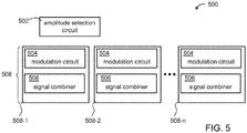
- FIG. 5 is a schematic block diagram illustration of phase shifter system 500, in embodiments of the invention in which system 500 comprises a circuitry array 508.
- Circuitry array 508 has a plurality of array elements 508-1, 508-2 etc, each having a respective modulation circuit 504 and a respective signal combining circuit 506, and may optionally, but not necessarily, also have a respective amplitude selection circuit.
- a phase-shifted signal formed at each array element is used as a reference signal at a subsequent array element, if present.
- FIG. 6 is a flowchart diagram of a method suitable for amplifying a phase shift of a signal relative to a reference signal, according to some embodiments of the present invention.
- the method begins at 600 and continues to 601 at which a signal S is generated or received, and to 602 at which a reference signal S ref is generated or received.
- a signal S For example, one of the signals (e.g ., signal S ) can be received following an interaction of that signal with an object, and the other signal (e.g ., signal S ref ) can be received via a path that does not allow it to interact with the object.
- a relative noise fluctuation of a signal is defined as the fluctuation of the signal from its baseline, expressed as a fraction or multiplication of the baseline.
- the average ( e.g., the Root-Mean-Square) of n ( t ) is denoted ⁇ n and the average ( e.g., the Root-Mean-Square) of n ref ( t ) is denoted ⁇ ref .
- both signal S and reference signal S ref are characterized by generally the same (e.g ., within 10%) relative noise fluctuation average. This can be ensured, for example, by using the same generator for generating S ref and for generating a transmitted output signal that interacts with an object to provide the signal S .
- the method continues to 603 at which the modulation of at least one of the signals is varied.
- the variation is optionally and preferably with respect to the modulation amplitude such that the modulation amplitudes of the signal and the reference signal are sufficiently close to each other.
- a ratio between modulation amplitudes of the signal and the reference signal is from about 0.9 to about 1.1, or from about 0.95 to about 1.05, or from about 0.99 to about 1.01, or from about 0.995 to about 1.005, or from about 0.999 to about 1.001 or from about 0.9995 to about 1.0005 or from about 0.9999 to about 1.0001.
- the expected amplification factor G is typically about 1/ ⁇ , where ⁇ is the absolute value of the difference between 1 and the ratio between modulation amplitudes of the signals.
- G and the aforementioned noise fluctuation averages are selected such that their product is less than 0.4 or less than 0.3 or less than 0.2 or less than 0.1 or less than 0.01 or less than 0.001.
- the noise fluctuation averages can be higher, namely XG is not necessarily less than q.
- a bandpass filter is employed with sufficiently narrow bandwidth as further detailed hereinabove.
- the variation is optionally and preferably also with respect to the modulation phase, such that the phase difference ⁇ in between the phase ⁇ 1 of the reference signal and the phase ⁇ 2 of the signal is sufficiently close to ⁇ radians, as further detailed hereinabove.
- one of signals S and S ref is generated by selected operations of method 100 so as to ensure that the phase difference ⁇ in is sufficiently small or sufficiently close to ⁇ radians.
- the amplitude(s) and phase(s) employed for the modulation variation can be selected by the method or be stored or encoded in a circuit that vary the modulation.
- the method preferably continues to 604 at which an output signal S out which is a linear combination of the signals is formed.
- This can be done electronically, using an electric circuit, or optically using an optical assembly as further detailed below.
- the combination 604 can be done either directly, for example, using a signal summing circuit, or indirectly, for example, by signal multiplication followed by extraction of signal components that are linearly proportional to each of the signals, as further detailed hereinabove.
- the normalization parameter p can be set to any number, e.g., 1.
- the linear combination coefficient reflects the weight ratio of the two signals and is optionally and preferably selected based on the sign of the cos( ⁇ in ). Generally, q is about 1 when cos( ⁇ in ) is negative and about -1 when cos( ⁇ in ) is positive.
- the amplification extent can reach the value of 1/ ⁇ , where ⁇ is the absolute value of the difference between 1 and the ratio between modulation amplitudes of the signals.
- ⁇ can be at most 0.1 or at most 0.05 or at most 0.01 or at most 0.005 or at most 0.0001 or less, so that ⁇ out can be 10 times larger or 20 times larger or 100 times larger or 200 times larger or 1000 times larger or 2000 times larger or 10000 times larger than ⁇ in .
- the formed output signal is filtered by a bandpass filter so as to improve the signal-to-noise ratio of the output signal.
- the bandwidth of the filter is preferably narrow.
- the bandwidth BW of the filter is at most f / ⁇ G , where f is a frequency of the output signal.
- the bandwidth BW of the filter is selected such that once the output signal is filtered the multiplication ⁇ out G is less than q, where ⁇ out is the noise fluctuation average ( e.g ., RMS) of the output signal.
- the operations described above can be repeated in iterative manner so as to provide a further amplification.
- the formed output signal is used as the as the input signal for the repetition.
- the method continues to 605 at which the phase of the output signal relative to the reference signal is measured.
- phase measuring technique including, without limitation, phase detectors that are commercially available from Mini-Circuits®, USA, and On Semiconductors®, USA.
- the method continues to 606 at which a change over time of the phase of the output signal relative to the reference signal is measured.
- Operation 606 can be executed whether or not the phase of the output signal is known, since a change in a phase of a signal can be measured even when the signal's phase itself is not known.
- 605 is executed and 606 is not executed, in some embodiments both 605 and 606 are executed, in some embodiments 605 is not executed and 606 is executed, and in some embodiments none of 605 and 606 is executed.
- FIG. 7 is a schematic block diagram illustration of a system 700 for amplifying a phase shift of a signal relative to a reference signal, according to some embodiments of the present invention.
- System 700 is optionally and preferably configured for executing one or more operations of method 600 above.
- System 700 comprises a modulation circuit 702, configured for varying a modulation of at least one of the signals as further detailed hereinabove.
- the amplitude(s) and phase(s) employed for the modulation variation performed by circuit 702 can be selected by system 700, for example, using an amplitude selection circuit (not shown, see FIG. 4 ), or be stored or encoded in circuit 702.
- System 700 can also comprise a signal combiner 704, configured for forming an output signal S out which is a linear combination of the signals, as further detailed hereinabove.
- combiner 704 comprises a signal multiplier circuit. These embodiments are useful when the linear combination is obtained by multiplication followed by extraction of linear components as further detailed hereinabove.
- combiner 704 is an optical assembly configured for performing a linear combination of two signals as known in the art, as further detailed hereinabove with respect to system 500.
- system 700 comprises a detector circuit 706, which can configured as phase detector for measuring a phase of the output signal relative to the reference signal, or as a phase-change detector for measuring a change of phase of the output signal over time, or as a combined phase detector and phase-change detector for measuring both the phase of and its change.
- a detector circuit 706 can configured as phase detector for measuring a phase of the output signal relative to the reference signal, or as a phase-change detector for measuring a change of phase of the output signal over time, or as a combined phase detector and phase-change detector for measuring both the phase of and its change.
- System 500 and/or system 700 can be employed in many applications. Generally, one or both these systems can be used in any system in which it is desired to phase-shift a signal and/or to measure a phase shift of the signal.
- Representative examples of systems suitable for the present embodiments including, without limitation, a system for measuring an internal structure of an object, a system for measuring a distance to an object, a system for measuring a motion characteristic of an object, an interferometer system, a system for measuring flow of fluid (gas or liquid), a radiofrequency transceiver system, an optical transceiver system, a communication system, a signal generating system and the like.
- system 500 and/or system 700 can be used in a sensing system that measures one or more characteristics of an object.
- a modulated signal interacts with the object.
- a change in the modulation of the signal is analyzed to extract one or more characteristics of an object, wherein the characteristics can relate to the structure of the object, the position of the object, the motion of the object or the thermal state of the object.
- the transmission of modulated signal to the object can comprise using system 500 above for generating a predetermined phase shift between the transmitted modulated signal and a reference signal.
- the analysis can comprise detecting the phase of the signal received from the object. This can be done by amplifying the phase using system 700 and then analyzing the amplified phase as known in the art.
- the reference signal that is used for the amplification performed by system 700 can be generated by system 500.
- system 700 and system 500 operate in concert wherein system 500 generates a reference signal S ref at such a phase that ensures with a predetermined phase-shift division factor that the phase difference between the reference signal S ref and the received signal S is sufficiently small or sufficiently close to ⁇ radians, and system 500 combines the two signal to effect phase amplification.
- phase of the reference signal may depend upon one or more of the characteristics of an object and deviations from those one or more of the characteristics.
- phase of the reference signal may depend upon the median position of the object and the small deviations from this position. Such deviations can be due to motion of a moving target object, to scanning of a set of points of a stationary target object, where the points on the target are at different depth positions, or to some combination of motion and varying depth locations of the scanned points on the target object.
- the value of reference phase is changed in a controlled fashion (e.g ., sawtooth, linear, sinusoidal or some other controlled scan of the values of the reference phase) using a phase shifter such as phase shifter system 500, while simultaneously monitoring the values of ⁇ ⁇ ut .
- a phase shifter such as phase shifter system 500
- the value of the reference phase for which ⁇ in is sufficiently small or sufficiently close to ⁇ radians can be determined, and therefore the change in the position of the target object can be determined.
- the value of the reference phase is changed in a controlled fashion (e.g., sawtooth, linear, sinusoidal or some other controlled scan of the values of the reference phase) using a phase shifter such as phase shifter system 500 while simultaneously monitoring the values of the modulation amplitude B of the received signal, and with the aid of a priori knowledge of the characteristics of the graph of B vs. the reference phase and vs. the deviation of ⁇ in from 0 or ⁇ and appropriate data processing, the value of the reference phase for which ⁇ in is sufficiently small or sufficiently close to ⁇ radians.
- the output signal is subjected to signal analysis responsively to a variation in ⁇ in .
- the processing is optionally and preferably executed to determine the change in the deviation of ⁇ in from 0 or ⁇ .
- This change allows extracting information pertaining to the object from which the input signal is received.
- the change in the deviation of ⁇ in from 0 or ⁇ can be used for, e.g ., extracting information pertaining to a change in distance to the object.
- the distance to the target object is measured using known techniques, and a value for the reference phase determined by such measurement is used as an input.
- known techniques which may be used to measure the distance to the target object include optical distance measurement techniques such as pulsed optical radar, phase-shift optical radar, and triangulation, linear encoding, and other optical or non-optical distance measurement means known in the art.
- known techniques measure the distance to the target object with lower precision than the method described herein.
- the value of ⁇ is scanned.
- the modulation amplitude of the output signal is monitored. Knowledge of the dependence of B on the deviation of ⁇ in from 0 or ⁇ (and therefore on the reference phase) as described in the examples section that follows (see, e.g., FIG. 12 ), allows the value of the physical parameter and its variation to be determined.
- the received signal comprises a signal reflected from the object, e.g., by diffuse reflection or specular reflection.
- the received signal comprises a signal scattered from the object, in some embodiments, the scattering is selected from the group consisting of Rayleigh scattering, Mie scattering, Tyndall scattering, Brillouin scattering and Raman scattering.
- the received signal comprises a signal absorbed by the object and re-emitted therefrom.
- the interaction with the object comprises a linear interaction.
- the interaction with the object comprises a non-linear interaction. In some of the nonlinear interactions the object concurrently interacts with the generated modulated signal and another different signal, e.g., is illuminated with a light source that is not related to the modulated signal.
- the interaction of the modulated signal with the object results in a change of the signal type, such that the generated modulated signal is of one type and the received signal is of another type.
- the object is an optoelectronic device, such as a detector
- the generated signal may be an electromagnetic signal entering the device
- the received signal may be an electric signal exiting the device.
- such an optoelectronic device may be used as a sensor which is sensitive to a parameter P of another object, or a parameter of the optoelectronic device itself may be sensed.
- the object includes a physical parameter which causes the shift between the modulation phase of the transmitted modulated signal and the received signal.
- the physical parameter comprises change in time-of-flight of the generated signal during the interaction with the object.
- the physical parameter may be any physical parameter which affects the time of flight of the signal.
- the change comprises a change in the time of flight of the signal during the time interval between entering and exiting the medium of the object, such as due to a different propagation velocity.
- the interaction comprises reflection or scattering of the signal following impingement on the object
- a change in time of flight can result when detecting impingement on a moving object as a result of changes in distance or when scanning a surface as a result of irregularities of the surface.
- the physical parameter comprises a change in the refractive index of the object or a medium thereof.
- any physical parameter that affects the refractive index may be monitored as described hereinbelow.
- Such physical parameters include, for example, electromagnetic carrier frequency of electromagnetic signals, stress, strain, temperature, electric field, magnetic field, material polarization, electromagnetic polarization, absorption, linear optical effects, nonlinear optical effects, linear electromagnetic effects, nonlinear electromagnetic effects (such as the presence of another electromagnetic field), and the presence or change of additional media such as biological media, organic media, inorganic media, hazardous or polluting media.
- the physical parameter comprises a change in the response time of the receipt of the signal from the object.
- certain characteristics or parameters of the object may change in the amount of time between the absorption of the signal and the retransmission thereof, resulting in a change in the response time of receipt of the signal from the object.
- the change in response time comprises a change in the response time of the medium in emitting the received signal after the generated modulated signal enters the medium.
- the change in response time can be due to changes in one or more of the material parameters of the medium (such as electrical, mechanical, optical parameters of the medium, etc.), the parameters of the wave of the generated modulated signal (such as power, carrier frequency, modulation frequency, etc.), and/or external parameters (such as temperature, stress, strain, etc).
- the material parameters of the medium such as electrical, mechanical, optical parameters of the medium, etc.
- the parameters of the wave of the generated modulated signal such as power, carrier frequency, modulation frequency, etc.
- external parameters such as temperature, stress, strain, etc.
- the physical parameter comprises a parameter which causes a change in the absorption of the generated modulated signal by the object or by interaction therewith. In some embodiments the physical parameter comprises a parameter which causes a change in the amplification of the generated modulated signal by the object or by interaction therewith. In some embodiments the physical parameter comprises a parameter which causes a change in the scattering of the generated modulated signal by the object or by interaction therewith. In some embodiments the physical parameter comprises a parameter which causes a change in the reflection coefficient of the object. In some embodiments the physical parameter comprises a parameter which causes a change in the transmission coefficient of the object.
- the physical parameter comprises any one or more of a change in the carrier frequency (for example via a non-linear effect with the medium), temperature, stress, strain, voltage, radiation polarization, material polarization, and the presence or change of an additional media such as biological media, organic media, inorganic media, hazardous media, and polluting media.
- the object comprises an optical fiber or waveguide. In some embodiments the object comprises a metallic wire or waveguide. In some embodiments, the object comprises a radiation detector. In some embodiments, the object includes a medium comprising water. In some embodiments, the object includes a medium comprising an inorganic liquid. In some embodiments, the object includes a medium comprising an organic liquid. In some embodiments, the object includes a medium comprising a physiological medium, such as tissue, blood, saliva, urine, and the like. In some embodiments, the object comprises a semiconductor, and includes a semiconductor medium. In some embodiments, the object includes a medium comprising a gain medium, such as an optical gain medium, an electromagnetic gain medium, or an electric gain medium. In some embodiments, the object includes an interface between two types of media, for example an interface between a metallic medium and a dielectric medium.
- any type of signal can be employed as a carrier for signals S and S ref .
- one or both signals is carried by an electromagnetic wave such as an optical beam
- one or both signals is carried by a mechanical wave (e.g ., ultrasound signal, sonic signal, infrasonic signal)
- one or both signals is carried by an electrical carrier (e.g., AC current) flowing in a conductive transmission line.
- the signals S and S ref can be carried by the same or different types of carriers, and the carrier frequencies of the signal S and S ref can be the same or they can differ.
- the modulation frequency can be the same or less than the carrier frequency of the respective signal.
- the modulation frequency of S and S ref can be in a sub-kilohertz range (e.g., 0.001Hz-999Hz), kilohertz range (e.g., 1kHz-999kHz), or a megahertz range ( e.g., 1MHz-999MHz), or gigahertz range ( e.g., 1GHz-999GHz).
- modulation frequency of S and S ref can be in radiofrequency range (e.g., 3Hz - 300 MHz), or the microwave range (e.g., 300 MHz - 300 GHz), or a sonic range (e.g., 20Hz - 20 kHz), or an ultrasonic range (e.g., 20kHz - 10GHz or 20 kHz - 5GHz), or an infrasonic range (e.g., 0.001 Hz - 20 Hz).
- radiofrequency range e.g., 3Hz - 300 MHz
- the microwave range e.g., 300 MHz - 300 GHz
- a sonic range e.g., 20Hz - 20 kHz
- an ultrasonic range e.g., 20kHz - 10GHz or 20 kHz - 5GHz
- infrasonic range e.g., 0.001 Hz - 20 Hz.
- any of the above types of signals can be generated by suitable signal generators as known in the art.
- a signal generator selected from the group of a function generator, an arbitrary waveform generator, an RF signal generator, a microwave signal generator, a vector signal generator, a logic signal generator, a radio transmitter, a vacuum tube, a klystron, a travelling-wave tube, a gyrotron, a magnetron, a field-effect transistor, a tunnel diode, a Gunn diode, IMPATT diode, a maser, backward wave oscillator, a synchrotron, a photomixer, a resonant tunneling diode, a laser, a LED and a lamp, can be used.
- a signal generator selected from the group consisting of a pitch generator, an acoustic transmitter, a transducer, electro-acoustic transducer/array, a speaker, a loudspeaker, a subwoofer loudspeaker, a rotary woofer, an engine and a plasma sound-source can be used.
- an electrical current modulator selected from the group of a pulse width modulator, a delta-sigma modulator, pulse-amplitude modulator, pulse-code modulator, pulse-density modulator, pulse-position modulator and a space-vector modulator can be used.
- the signal generator comprises a digital computation component.
- the signals S and S ref are both electric signals.
- one or more of the signals is non-electric (e.g ., electromagnetic, mechanical) and in some embodiments is converted to an electric signal ( e.g., by an electromagnetic detector or a mechanical wave detector) so that both S and S ref are eventually electric signals.
- the output signal generator comprises an electronic summing circuit.
- a method of generating a signal being phase-shifted at a predetermined phase-shift division factor relative to a reference signal comprises: using the predetermined phase-shift division factor for selecting a modulation amplitude; modulating a control signal at the selected modulation amplitude, wherein a cosine of a phase difference between the reference signal and the control signal, in absolute value, is at least 0.5; and combining the reference signal and the control signal to form the phase-shifted signal.
- the method comprises generating at least one of the control signal and the reference signal.
- the method comprises selecting a value of a phase of the control signal based on the selected modulation amplitude.
- the method comprises selecting a value of a phase of the control signal, wherein the selection of the modulation amplitude is based also on the selected phase.
- the method comprises sequentially repeating the selection of the modulation amplitude, the modulation of the control signal and the combining at least once, each time using a previously formed phase-shifted signal as the reference signal.
- a phase shifter system comprising: an amplitude selection circuit, configured for selecting, based on a predetermined phase-shift division factor, a modulation amplitude; a modulation circuit, configured for modulating a control signal at the selected modulation amplitude, wherein a cosine of a phase difference between the reference signal and the control signal, in absolute value, is at least 0.95; and a signal combiner configured for combining the reference signal and the control signal to form a phase-shifted signal relative to the reference signal.
- the modulation circuit is a signal generation and modulation circuit configured for generating at least one of the control signal and reference signal.
- the system comprises a circuitry array having a plurality of array elements, each having at least one of: a respective amplitude selection circuit, a respective modulation circuit and a respective signal combiner, wherein a phase-shifted signal formed at each array element is used as a reference signal at a subsequent array element, if present.
- the selected modulation amplitude is substantially smaller than a modulation amplitude of the reference signal.
- a ratio between the modulation amplitude of the reference signal and the selected modulation amplitude is at least 5. According to some embodiments of the invention a ratio between the modulation amplitude of the reference signal and the selected modulation amplitude is at least 10. According to some embodiments of the invention a ratio between the modulation amplitude of the reference signal and the selected modulation amplitude is at least 100. According to some embodiments of the invention a ratio between the modulation amplitude of the reference signal and the selected modulation amplitude is at least 1000.
- the combining comprises summing.
- the combining comprises multiplication to provide a multiplication signal, followed by extraction from the multiplication signal components being linearly proportional to each of the reference signal and the control signal.
- a method of amplifying a phase shift of a signal relative to a reference signal comprises: varying a modulation of at least one of the signals such that a ratio between modulation amplitudes of the signal and the reference signal is at least 0.9 and at most 1.1, and a cosine of a phase difference between the reference signal and the signal, in absolute value, is at least 0.95; and forming an output signal which is a linear combination of the reference signal and the signal, following the variation, the linear combination being characterized by a linear combination coefficient which is within 10% from an additive inverse of a nearest integer of the cosine.
- the method comprises generating at least one of the signals.
- the method comprises measuring a phase of the output signal relative to the reference signal.
- the method comprises measuring a change of phase of the output signal over time.
- a system for amplifying a phase shift of a signal relative to a reference signal comprises: a modulation circuit, configured for varying a modulation of at least one of the signals such that a ratio between modulation amplitudes of the signal and the reference signal is at least 0.9 and at most 1.1, and a cosine of a phase difference between the signal and the reference signal, in absolute value, is at least 0.95 and less than 1; and a signal combiner configured for forming a linear combination of the signals, following the variation, the linear combination being characterized by a linear combination coefficient which is within 10% from an additive inverse of a nearest integer of the cosine.
- the modulation circuit is a signal generation and modulation circuit configured for generating at least one of the signal and the reference signal.
- the system comprises a phase detector circuit configured for measuring a phase of the output signal relative to the reference signal.
- the system comprises a phase-change detector circuit configured for measuring a change of phase of the output signal over time.
- the linear combination is formed by a signal summing circuit.
- the linear combination is formed by a signal subtraction circuit.
- the linear combination is formed optically.
- the linear combination is formed by multiplying the signal to provide a multiplication signal, and extracting from the multiplication signal components being linearly proportional to each of the signals.
- a system for measuring an internal structure of an object comprising the system as delineated above and optionally and preferably as further detailed below.
- a system for measuring a distance to an object comprising the system as delineated above and optionally and preferably as further detailed below.
- a system for measuring a motion characteristic comprising the system as delineated above and optionally and preferably as further detailed below.
- an interferometer system comprising the system as delineated above and optionally and preferably as further detailed below.
- a system for measuring flow comprising the system as delineated above and optionally and preferably as further detailed below.
- a radiofrequency transceiver comprising the system as delineated above and optionally and preferably as further detailed below.
- an optical transceiver comprising the system as delineated above and optionally and preferably as further detailed below.
- a communication system comprising the system as delineated above and optionally and preferably as further detailed below.
- the absolute value of the cosine is at least 0.99. According to some embodiments of the invention the absolute value of the cosine is at least 0.995. According to some embodiments of the invention the absolute value of the cosine is at least 0.999. According to some embodiments of the invention the absolute value of the cosine is at least 0.9995. According to some embodiments of the invention the absolute value of the cosine is at least 0.9999.
- a modulation frequency of both the reference signal and the control signal is in a radiofrequency range. According to some embodiments of the invention a modulation frequency of both the reference signal and the control signal is in a sub-kilohertz range. According to some embodiments of the invention a modulation frequency of both the reference signal and the control signal is in a kilohertz range. According to some embodiments of the invention a modulation frequency of both the reference signal and the control signal is in megahertz range. According to some embodiments of the invention a modulation frequency of both the reference signal and the control signal is in gigahertz range.
- each of the signals is carried by a carrier electrical signal, wherein a modulation frequency of both the reference signal and the control signal is at least 10 times lower than a carrier frequency of the carrier electrical signal.
- each of the signals is carried by a carrier ultrasound signal, wherein a modulation frequency of both the reference signal and the control signal is at least 10 times lower than a carrier frequency of the carrier ultrasound signal.
- each of the signals is carried by a carrier optical signal, wherein a modulation frequency of both the reference signal and the control signal is at least 10 times lower than a carrier frequency of the carrier optical signal.
- compositions, method or structure may include additional ingredients, steps and/or parts, but only if the additional ingredients, steps and/or parts do not materially alter the basic and novel characteristics of the claimed composition, method or structure.
- a compound or “at least one compound” may include a plurality of compounds, including mixtures thereof.
- range format is merely for convenience and brevity and should not be construed as an inflexible limitation on the scope of the invention. Accordingly, the description of a range should be considered to have specifically disclosed all the possible subranges as well as individual numerical values within that range. For example, description of a range such as from 1 to 6 should be considered to have specifically disclosed subranges such as from 1 to 3, from 1 to 4, from 1 to 5, from 2 to 4, from 2 to 6, from 3 to 6 etc., as well as individual numbers within that range, for example, 1, 2, 3, 4, 5, and 6. This applies regardless of the breadth of the range.
- the sum of two modulated signals (described by the formulas A 1 cos( ⁇ t + ⁇ 1 ) and A 2 cos( ⁇ t + ⁇ 2 )) having the same modulation frequency and different modulation phases, results in a new signal, having the same modulation frequency as the summed signals, and having a modulation amplitude and a modulation phase that depend upon the modulation amplitudes and modulation phases of the two summed signals, respectively, as described by the equation:
- Such comparative examples can be analyzed algebraically for ⁇ which is significantly smaller than 1, mathematically described by ⁇ ⁇ 1 so that g is significantly greater than 1, mathematically described as g >> 1.
- Equation (1.5) shows that in a certain range of ⁇ in for which cos ( ⁇ in ) does not change appreciably, such as when ⁇ in is substantially equal to ⁇ or when ⁇ in is substantially equal to 0, ⁇ ⁇ out ⁇ ⁇ ⁇ in / g
- FIGs. 8A-C graphically show that using the comparative example described hereinabove in which the value of ⁇ is constant, a large change in ⁇ in translates to a smaller change in ⁇ out , at various values of modulation phase shift dividing factor g .
- the input phase is in the range of -1.5 to 1.5 Rad.
- the input phase is in the range of -0.8 to 0.8 Rad.
- the change in the phase of the output signal is within a certain range approximately linearly proportional to the change in the input phase divided by g, or, written mathematically, ⁇ ⁇ out ⁇ ⁇ ⁇ in / g , over an input phase range of at least 1 radian.
- the amplitude B of the output signal varies by about 3%.
- the ratio ⁇ of the modulation amplitudes of the summed signals is varied in a controlled fashion.
- the proper value of ⁇ can vary for different values of ⁇ in .
- the output phase ⁇ out is equal to the input phase ⁇ in divided by 8
- the output phase ⁇ out is equal to the input phase ⁇ in divided by 128. It is appreciated that a similar procedure can be employed for other values.
- FIGs. 9A and 9B graphically show that using the comparative examples described in EQs. (1.7)-(1.13) a large change in ⁇ in translates to a smaller change in ⁇ out,N , at various stages N .
- N 3
- N 6.
- Both graphs illustrate that the change in the output phase ⁇ out,N is 2 N smaller than the change in the input phase ⁇ in .
- the graphs show that the amplitude B of the output signal varies as well, limiting the usable range of ⁇ in to approximately ⁇ radians. It is to be understood that other choices of ⁇ , for a given input phase ⁇ in are also possible and can result in ⁇ out ⁇ in /g.
- d ⁇ out d ⁇ in A ⁇ 2 + A ⁇ cos ⁇ in 1 + 2 A ⁇ cos ⁇ in + A ⁇ 2 and B ⁇ 1 + 2 A ⁇ cos ⁇ in + A ⁇ 2 .
- the derivative d ⁇ out /d ⁇ in and output amplitude B can be approximated as: d ⁇ out d ⁇ in ⁇ A ⁇ cos ⁇ in 1 + 2 A ⁇ cos ⁇ in and B ⁇ 1 + 2 A ⁇ cos ⁇ in , so that both d ⁇ out /d ⁇ in and B depends ⁇ in through the expression ⁇ cos( ⁇ in ).
- both ⁇ and ⁇ in are dependently varied in a manner that maintains ⁇ cos( ⁇ in ) generally constant. Such dependent variation can ensure that the both the derivative d ⁇ out /d ⁇ in and the output amplitude B remain generally constant.
- the user can control the value of g hence also the resolution of the phase shift of the output signal.
- the resolution of the output phase change ⁇ ⁇ out ⁇ ⁇ ⁇ in / g can be on the order of 0.10° or 0.010° or 0.001° or even less.
- FIG. 10 is a schematic representation of a comparative example of a system 10 for controlling the phase shift of a modulated signal.
- System 10 includes a signal generator 12, for generating a modulated signal S source , having a first portion defining a first modulated signal 14 and a second portion defining a second modulated signal 18.
- system 10 includes a first signal generator for generating a first modulated signal 14 and a second signal generator for generating a second modulated signal 18.
- first modulated signal 14 is received from another signal source (not shown) and signal generator 12 is used to generate second modulated signal 18.
- First modulated signal 14 is directed to one or more signal manipulators, including first amplitude controller 20 configured to adjust, or control, the modulation amplitude of signal 14, and a first phase controller 22, configured to adjust, or control, the modulation phase of signal 14.
- first amplitude controller 20 configured to adjust, or control, the modulation amplitude of signal 14
- first phase controller 22 configured to adjust, or control, the modulation phase of signal 14.
- a processed signal 24 is given by the formula A 1 cos( ⁇ t + ⁇ 1 ).
- Second modulated signal 18 is directed to one or more signal manipulators, including second amplitude controller 26 configured to adjust, or control, the modulation amplitude of signal 18, and a second phase controller 28, configured to adjust, or control, the modulation phase of signal 18.
- the signal output from second amplitude controller 26 and second phase controller 28, is a controlling signal 30, given by the formula A 2 cos( ⁇ t + ⁇ 2 ).
- the values of ⁇ in and ⁇ are set by controlling the modulation phase and modulation amplitude of only one of first and second modulated signals 14 and 18.
- amplitude controller 26 and phase controller 28 may be obviated.
- amplitude controller 20 and phase controller 22 may be obviated.
- Signal manipulators 20, 22, 26, and/or 28 may include any suitable signal manipulator, and may comprise a suitable amplifier known in the art.
- g is greater than 1, and in some comparative examples is set by the operator to be sufficiently large, such that large changes in the phase difference ⁇ in of the signals input to output signal generator 32 is translated by output signal generator 32 to small changes in the phase of the output signal 34.
- a small change ⁇ P in a physical parameter P of an object interacting with a signal affects a small change in the modulation phase ⁇ 1 of that signal, which phase change can be as characterized by the derivative d ⁇ 1 / dP.
- the sensitivity and G are within 50% of the maximal sensitivity as long as
- FIG. 11A displays a graph showing values of ⁇ out - ⁇ 1 as a function of the value of ⁇ (when ⁇ in is close to ⁇ ) or ⁇ in (when ⁇ in is close to 0).
- the maximum slope (sensitivity) corresponds to the region of small ⁇ in or ⁇ values.
- ⁇ 0.001
- ⁇ 0.101
- the region of high sensitivity is in the range of -0.101 ⁇ ⁇ , ⁇ in ⁇ 0.101.
- FIG. 11B displays plot 200 of FIG. 11A , over a smaller region around the value of small ⁇ or ⁇ in , to more clearly show the exact region of high sensitivity.
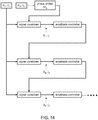
- FIG. 13 is a schematic representation of an embodiment of a system 400 for sensing the displacement of an object and for three dimensional imaging of an object using a method for quantifying a modulation phase shift of a modulated signal subsequent to interaction with the object according to an embodiment of the teachings herein.
- System 400 comprises a waveform generator 402 which generates a sinusoidal modulated signal 404 which modulates a light source 406.
- the light source may provide illumination at any suitable wavelength range, as further detailed hereinabove.
- Waveform generator 402 and light source 406 together define a signal generator 408 which emits a modulated light signal 410.
- the modulated light signal 410 is directed towards, and illuminates an object 412 located at a distance z 0 from the light source 406. Subsequently, the distance traversed by the light signal 410 from light source 406 to object 412 is changed by a distance dz. In some embodiments this occurs when illuminated object 412 changes its position by a distance dz, such that it is at a distance z 0 + dz from the light source 406.
- the new position of the object 412 is indicated by reference numeral 414. In other embodiments, this occurs when the modulated light signal 410 is directed at another point on object 412, which point is at a different distance from the light source 406.
- Light detector 418 provides as an output a received signal 420, which is a modulated (sinusoidal) signal.
- Received signal 420 has a modulation phase which corresponds to the modulation phase of light signal 416 reflected from object 412, and a modulation amplitude that is dependent upon several parameters, among them the alternating current (AC) power of the modulated light signal 410 and the reflection of the object 412 at its original location or at location 414.
- AC alternating current
- signal 420 is provided as an input to amplitude locker 422, which is configured to lock the modulation amplitude of signal 420 and, such that a sinusoidal modulated signal 424 provided as the output of amplitude locker 422 has a set modulation amplitude value, controlled by an operator of the system 400, and a modulation phase that corresponds to the modulation phase of signals 420 and 416.
- the modulation amplitude of signal 424 is independent of the modulation amplitude of signal 420 provided as input to amplitude locker 422.
- signal 424 has a constant modulation amplitude (which value is determined and set by the operator), and a modulation phase including a constant component (whose value is determined and set by the operator) and a component that changes proportionally with 2Kdz.
- setting of the modulation amplitude and/or of the constant component of the modulation phase can be accomplished by various electric circuits, for example in combination with an amplifier, as known in the art.
- waveform generator 402 Concurrently with directing of a signal 410 towards object 412 and receipt and processing of received signal 416, waveform generator 402 generates another modulated signal 426, and provides the modulated signal 426 to at least one signal manipulator 428.
- Signal manipulator 428 provides as output a reference signal 430.
- One or more signal manipulator 428 is configured to set the modulation amplitude and modulation phase of signal 426 to generate reference signal 430 as output.
- the modulation amplitude of reference signal 430 is set to be substantially equal to the modulation phase of signal 424, such that a ratio of the modulation amplitude of the reference signal 430 and the modulation amplitude of signal 424 is close to 1.
- the modulation phase of reference signal 430 is set to be offset from the modulation phase of signal 424 by an amount close to ⁇ radians (for an illuminated object at a distance of z 0 from the illuminating light source).
- reference signal 430 is set to be substantially in phase with signal 424, i.e., the modulation phase of reference signal 430 is set to be offset from the modulation phase of signal 424 by an amount close to 0 (for an illuminated object at a distance of z 0 from the illuminating light source).
- Signal 424 and reference signal 430 are provided to an output signal provider 432, which provides as output a modulated output signal 434.
- output signal provider 432 comprises a component, such as a signal-adder, configured to provide an output signal including the sum of AC portions of the signal 424 and of reference signal 430, or to provide an output signal having an AC component which is proportional to the sum of the AC components of signal 424 and of reference signal 430 at a modulation frequency of ⁇ .
- output signal provider 432 comprises a component, such as a signal subtractor, configured to provide an output signal including the difference between signal 424 and reference signal 430, or to provide an output signal having an AC component which is proportional to the difference of the AC components of signal 424 and of reference signal 430 at a modulation frequency of ⁇ .
- the modulated output signal 434 has an output signal modulation amplitude of B and an output signal modulation phase, which output signal modulation phase changes with displacement of magnitude dz of object 412. Due to the modulation phase amplification factor of signal 424, the output signal modulation phase of modulated output signal 434 is amplified.
- Modulated output signal 434 is provided as an input to a modulation phase measurer 436.
- Modulation phase measurer 436 identifies and quantifies the values of the output signal modulation phase and/or of changes to the output signal modulation phase, and provides as output an output signal modulation measure signal 438, representing the output signal modulation phase and/or phase changes thereto.
- modulated output signal 434 may be provided as an input to a modulation amplitude measurer (not shown) in addition to, or instead of, being provided to modulation phase measurer 436.
- the modulation amplitude measurer identifies and quantifies the values of the output signal modulation amplitude B and/or of changes to the output signal modulation amplitude ⁇ B , and provides as output an output signal modulation measure signal 438 representing the output signal modulation phase B and/or changes ⁇ B thereto.
- Output signal modulation measure signal 438 is provided as an input to an electronic calculation system 440.
- the value of dz computed by electronic calculation system 440, and in some embodiments also a measure of the distance z 0 at which object 412 was displaced, is output from electronic calculation system 440 as a parameter change signal 442.
- the parameter change signal 442 is provided to the operator via a user interface 444, such as a memory, display, speaker, or transmitting system.
- the depth resolution is approximately 1 cm and the size of the maximal depth window is given by 2 ⁇ z max ⁇ 50cm, with 25 resolution points.
- the main elements of the embodiment of FIG. 13 described hereinabove can be implemented for two-dimensional (2D) or three-dimensional (3D) imaging, such as for topography mapping, computer gaming, radar and other applications.
- various technological elements and method may be used, such as using an array of detectors such as CMOS-based arrays or other types of detector arrays together with imaging optics to image n x m volume pixels (voxels) in parallel, while changing the direction of the illumination beam in two-dimensions (e.g., elevation and azimuth) to "scan" a region.
- an array of detectors such as CMOS-based arrays or other types of detector arrays together with imaging optics to image n x m volume pixels (voxels) in parallel, while changing the direction of the illumination beam in two-dimensions (e.g., elevation and azimuth) to "scan" a region.
- This Example presents a technique for RF phase-shift amplification based on RF interferometry and demonstrates it in an optical system.
- This Example shows that the input phase noise is not amplified together with the input phase signal, so that the phase sensitivity improves with higher phase-shift amplification.
- This Example predicts that in the case of correlated amplitude noise, the sensitivity is not affected by amplitude noise.
- a phase-shift resolution of 0.2 mrad is demonstrated, giving 8 ⁇ m distance resolution. It is envisioned that nanometric distance resolution can be achieved, for example, with sub-GHz modulation.
- phase-shift radar Many applications in RF radar and sensing, including RF photonic applications, require the sensitive detection or manipulation of the RF phase shift [1-9].
- displacement and velocity sensing such as phase-shift radar
- vector network analysis of the RF magnitude and phase spectrum is desired.
- phase-shift sensitivity of conventional applications are limited by the capabilities of conventional RF phase detectors to a minimum value of approximately 1 degree, due to nonlinear effects as well as noise.
- This Example describes a phase-shift amplifier that is based on destructive interference between two sinusoidal signals.
- This amplifier is particularly useful for "boosting" small phase shifts before applying phase detection. It is show below that this phase-shift amplification technique does not amplify the input phase noise, which is the dominant noise in these systems. Therefore, as opposed to conventional amplifiers, the phase-shift sensitivity improves with the phase-shift gain of the amplifier.
- Another attractive feature of this amplifier is the fact that it preferably does not amplify amplitude noise as well if this noise fulfills a correlation condition that will be described below.
- phase-shift i.e., approximately 0.01 degree
- Nanometric resolution is predicted as well with sub-GHz modulation frequencies.
- FIG. 15 A basic block diagram of a system based on this technique for amplifying small phase shifts, taking as an example the measurement of a small displacement ⁇ z , is illustrated in FIG. 15 .
- An RF signal A 0 cos ⁇ t irradiates a target and returns as A 0 cos( ⁇ t+ ⁇ 2 ), where it is summed with a reference signal A 0 cos( ⁇ t+ ⁇ 1 ) to form Bcos( ⁇ t+ ⁇ ).
- the output phase ⁇ ⁇ ut is enacted by ⁇ .
- n the refractive index of the medium at which the signal propagates.
- the two dashed arrows in FIG. 15 symbolize an RF signal which may be modulated on an optical carrier, other electromagnetic radiation, or alternatively a purely electronic signal.
- the measuring path may be free space or some other medium.
- an application in distance measurement is shown.
- the measurement of any parameter which affects the RF phase e.g ., characterization of microwave systems or dielectric materials is also contemplated.
- a first type of noise source includes input phase noise on ⁇ 1 and ⁇
- a second type of noise source includes noise fluctuations of G which are due to amplitude noise on A 1 and A 2 .
- ⁇ ⁇ 2 0 ⁇ ⁇ 1 0 ⁇ ⁇ + ⁇ t + ⁇ sig
- ⁇ ( t ) ⁇ 2 ( t ) - ⁇ 1 ( t )
- the spectral power of the input phase noise is typically sharply centered around the RF carrier.
- the effective phase-noise bandwidth is less than 10 Hz [12].
- the amplitude noise is typically broader in bandwidth and more amicable to filtering. As is shown below, in certain cases the input amplitude noise does not degrade performance at all.
- ⁇ sig,min The minimum detectable phase-change in the presence of noise.
- the expression G 0 ⁇ n is selected sufficiently smaller than 1, as further detailed hereinabove.
- EQs. 3.11 and 3.12 predict that the amplifier's phase-change sensitivity degrades in proportion to the phase-noise of the source and improves for higher values of the phase-change amplification factor. This is a desirable property of a phase-shift amplifier, and is due to the fact that the phase-noise of the source is not amplified together with the phase-change signal. Another prediction is that when the noise is mutually correlated on the summed signals, the sensitivity is not degraded by amplitude noise ⁇ n which is also a desirable feature.
- FIG. 16 An optical realization of RF phase-shift amplification with correlated phase noise and uncorrelated amplitude noise according to some embodiments of the present invention is illustrated schematically in FIG. 16 .
- P peak phase deviation
- P/V2 for sinusoidal noise
- the output of the generator directly modulated the two lasers in the 1550nm region, each with an output power of about 1 mW.
- Laser 2 illuminated a mirror and the reflection entered a detector together with a reference beam from Laser 1.
- solid and dashed lines are the electrical and optical signals respectively.
- the difference in RF phase between the signal and reference beams at the detector was set to ⁇ (by adding a phase delay of 2 KL + ⁇ to beam 1), and the amplitude ratio ⁇ was set to give the desired G 0 .
- the detector output is proportional to the sum of the two RF signals.
- the detector AC output was 500 mV peak-to-peak.
- the AC output was reduced by a factor 1/ G 0 due to the destructive interference, so that at the maximum gain of 100 the output signal was approximately 5 mV peak-to-peak.
- the peak deviation of the phase-noise on the output phase ⁇ ( t ) was measured while varying G 0 , in order to verify that the dominant phase noise is the sinusoidal phase noise which was impressed on the input, and to prove the prediction that the phase noise is not amplified.
- the spectrum for P ⁇ 1 consisted of a carrier at 600MHz and two sidebands at an offset frequency of ⁇ 1KHz.
- FIG. 17 is a graph showing the peak phase deviation of the output phase noise as a function of G 0 .
- the solid line corresponds to the theory and the dots correspond to the experimental data.
- the bandwidth BW of the filter that can ensure sufficient SNR and phase-noise limited operation, is inversely proportional to G 0 , since the output signal amplitude is also inversely dependent on G 0 .
- a second experiment was directed to the verification that the phase-shift amplification technique of the present embodiments can be useful for enhancing the resolution of distance measurement.
- FIG. 18 is a graph showing the output phase-change signal, ⁇ sig as a function of the input phase-change signal, ⁇ sig , for three values of G 0 : (a) 10, (b) 50 and (c) 100.
- FIG. 19 is a graph showing the minimum phase change as a function of G 0 , and which demonstrate that ⁇ sig,min is proportional to 1/ G 0 .
- the phase-shift amplification was achieved in the optical domain, by summing the intensity of two beams that are optically incoherent with the use of a beam splitter and an optical detector.
- this amplification can also be achieved electronically, e.g., using an RF summer.
- two or more stages of amplification are concatenated, where each amplification stage can be either electronic or optical. Since the output amplitude is reduced by a factor G 0 , linking more than one stage, with proper signal amplitude amplification and control between the stages, would be a good approach for effectively achieving high phase-shift amplification.
- the effective phase noise is approximately 0.01° and ⁇ ⁇ / f 0 ⁇ 2 x 10 -12 [ rad ⁇ s ] .
- This corresponds to ⁇ z min ⁇ 5 ⁇ 10 ⁇ 5 G 0 m with an SNR of unity, and reflects best performance without accounting for further additive system noise.
- a resolution of about 5 ⁇ m is achievable.
- the ability to reach nanometric sensitivity with relatively low RF frequencies may ultimately be used as an alternative to coherent optical interferometry or other techniques.
- the present Inventors also contemplate use of any of the techniques disclosed, for example, in references 2 and 6-10 as a phase detection stage applied after the phase-shift technique described herein.
- the present embodiments provide the ability to boost small phase-shifts before the phase detection process takes place, without amplifying the phase noise or amplitude noise as well. Therefore, for any given RF operating frequency, the technique of the present embodiments can reach higher sensitivity than other types of phase amplifiers.
- An exemplified system 800 that provides a two-stage amplification in which in a first stage the signal are processed optically and in a second stage the signals are processed electrically have been devised according to some embodiments of the present invention.
- phase amplification is achieved by summing the intensity of two beams that are optically incoherent using a beam splitter and an optical detector.
- phase amplification is achieved electronically, with an electrical combiner.
- FIG. 20A is a conceptual block diagram of the system, showing an optical amplification system 802 and an electrical amplification system 804.
- the optical amplification system 802 provides a first amplification of the phase shift and the electrical amplification system 804 further amplifies the phase shift.
- the optical amplification system 802 is schematically illustrated in FIG. 20B .
- a signal generator 803 provides an electrical signal to a laser device 805.
- the laser device 204 transmits a transmitted optical beam 814 to an object 810.
- Beam 814 interacts with object 810 to provide another beam 810.
- Beam 810 constitutes the signal S ( FIG. 1 ) of amplification system 802.
- Laser 805 also transmits a beam 816 to an amplitude and phase control 806 at which beam 816 is modulated to provide a reference beam 808.
- Beam 808 constitutes the reference signal S ref ( FIG. 1 ) of amplification system 802.
- Both beams 808 and 810 arrive at a photodetector which receives the optical beams and provides an output electrical signal 818 which constitutes a linear combination of S and S ref as further detailed hereinabove.
- dashed lines represents optical beams and solid lines represent electrical signals.
- the electrical amplification system 804 is schematically illustrated in FIG. 20C .
- Signal 822 is transmitted to an electrical signal mixer 826 (e.g., an RF mixer), and signal 824 is transmitted to an electrical signal mixer 828 ( e.g., an RF mixer).
- Mixer 826 also receives signal 818 from system 802, and mixer 828 also receives a signal 830 that has the same phase and frequency as signal 816 generated by laser 804 of system 803. Both mixers 826 and 828 mix the signals they receive and output mixed electrical signals, denoted signal 832 and signal 834, respectively.
- Signal 832 constitutes the signal S ( FIG. 1 ) of amplification system 804.
- Signal 834 is transmitted to an amplitude and phase control 835 at which signal 835 is modulated to provide a reference signal 837.
- Signal 837 constitutes the reference signal S ref ( FIG. 1 ) of amplification system 804.
- Signals 832 and 837 are combined at a signal combiner 836, which outputs a combined signal 838.
- combiner 836 is a summing circuit, in which case signal 838 is the sum of signals 832 and 837.
- Both signals 832 and 837 are at a frequency of about ⁇ - ⁇ , so that system 804 operates at frequencies that are significantly lower than the frequencies at which system 802 operates.
- signal 838 is filtered by a band pass filter 840 to provide a filtered signal 842.
- FIG. 20D A more detailed illustration of system 800, including both systems 802 and 803 is provided in FIG. 20D .
Landscapes
- Engineering & Computer Science (AREA)
- Computer Networks & Wireless Communication (AREA)
- Signal Processing (AREA)
- Optical Modulation, Optical Deflection, Nonlinear Optics, Optical Demodulation, Optical Logic Elements (AREA)
- Physics & Mathematics (AREA)
- General Physics & Mathematics (AREA)
Claims (15)
- Procédé d'amplification de déphasage, le procédé comprenant :recevoir un signal d'entrée en réponse à un signal de sortie émis ;générer un signal de référence ;faire varier une modulation d'au moins l'un des signaux de telle sorte qu'un rapport entre des amplitudes de modulation du signal d'entrée et du signal de référence est d'au moins 0,9 et d'au plus 1,1, et une différence de phase entre le signal de référence et le signal d'entrée est d'environ 0,9π à environ 1,1π ;former un signal de sortie qui comprend une somme du signal de référence et du signal d'entrée, après ladite variation ; etfiltrer ledit signal de sortie par un filtre passe-bande pour former un signal de sortie filtré, une bande passante dudit filtre passe-bande étant choisie de telle sorte que XG<0,1, où X est une moyenne de fluctuation de bruit dudit signal de sortie filtré, et G est un facteur d'amplification attendu d'un déphasage entre ledit signal d'entré et ledit signal de référence.
- Procédé selon la revendication 1, comprenant en outre : mesurer une phase ou un changement de phase dudit signal de sortie par rapport au signal de référence.
- Procédé selon l'une quelconque des revendications 1 et 2, dans lequel ladite bande passante est d'au plus f/√G, où f est une fréquence dudit signal de sortie.
- Procédé selon l'une quelconque des revendications 1 à 3, comprenant en outre : répéter ladite variation et ladite formation, en utilisant ledit signal de sortie pour générer un signal d'entrée pour ladite répétition.
- Procédé selon l'une quelconque des revendications 1 à 3, dans lequel ledit signal d'entrée et ledit signal de référence sont des signaux optiques, dans lequel ledit signal de sortie est un signal électrique, et dans lequel le procédé comprend : générer un signal de référence électrique et répéter ladite variation et ladite formation, en utilisant ledit signal de sortie électrique et ledit signal de référence électrique.
- Système pour amplifier un déphasage, le système comprenant :un émetteur pour émettre un signal de sortie, et un récepteur pour recevoir un signal d'entrée en réponse audit signal émis ;un générateur de signal de référence pour générer un signal de référence ;un circuit de modulation, configuré pour faire varier une modulation d'au moins l'un des signaux de telle sorte qu'un rapport entre des amplitudes de modulation du signal d'entrée et du signal de référence est d'au moins 0,9 et d'au plus 1,1, et une différence de phase entre le signal de référence et le signal d'entrée est d'environ 0,9π à environ 1,1π ;un mélangeur de signaux configuré pour additionner les signaux, après ladite variation ; etun filtre passe-bande pour filtrer ledit signal de sortie afin de former un signal de sortie filtré, une bande passante dudit filtre passe-bande étant choisie de telle sorte que XG<0,1, où X est une moyenne de fluctuation de bruit dudit signal de sortie filtré, et G est un facteur d'amplification attendu d'un déphasage entre ledit signal d'entrée et ledit signal de référence.
- Système selon la revendication 6, comprenant en outre au moins l'un parmi : un circuit détecteur de phase configuré pour mesurer une phase dudit signal de sortie par rapport au signal de référence, et un circuit détecteur de changement de phase configuré pour mesurer un changement de phase dudit signal de sortie au cours du temps.
- Système selon l'une quelconque des revendications 6 et 7, dans lequel ladite bande passante est d'au plus f/√G, où f est une fréquence dudit signal de sortie.
- Système selon l'une quelconque des revendications 6 à 8, comprenant en outre un circuit de modulation supplémentaire et un mélangeur de signaux supplémentaire configurés pour répéter ladite variation et ladite formation, en utilisant ledit signal de sortie pour générer un signal d'entrée pour ladite répétition.
- Système selon l'une quelconque des revendications 6 à 8, dans lequel ledit signal d'entré et ledit signal de référence sont des signaux optiques, dans lequel ledit signal de sortie est un signal électrique, et dans lequel le système comprend un générateur de signal de référence électrique pour générer un signal de référence électrique, un circuit de modulation électrique configuré pour faire varier une modulation d'au moins l'un du signal de sortie électrique et du signal de référence électrique, et un mélangeur de signaux électriques pour former une combinaison linéaire du signal de sortie électrique et du signal de référence électrique, après ladite variation.
- Procédé selon l'une quelconque des revendications 1 à 5 ou système selon l'une quelconque des revendications 6 à 10, dans lequel ladite combinaison linéaire est formée par un circuit de sommation de signaux.
- Procédé selon l'une quelconque des revendications 1 à 5 ou système selon l'une quelconque des revendications 6 à 10, dans lequel ladite combinaison linéaire est formée optiquement.
- Système selon l'une quelconque des revendications 6 à 12, servant pour une opération choisie parmi le groupe consistant en : mesurer une structure interne d'un objet, mesurer une distance par rapport à un objet, mesurer une caractéristique de mouvement, réaliser une interférométrie, mesurer un écoulement, émettre et recevoir des signaux radiofréquences, émettre et recevoir des signaux optiques, et communiquer des informations.
- Procédé selon l'une quelconque des revendications 1 à 5 ou système selon l'une quelconque des revendications 6 à 13, dans lequel chacun du signal de référence et dudit signal d'entrée est transporté par un signal de porteuse, dans lequel une fréquence de modulation à la fois du signal de référence et dudit signal d'entrée est au moins 10 fois inférieure à une fréquence porteuse dudit signal de porteuse, et dans lequel ledit signal de porteuse est choisi parmi le groupe consistant en un signal électrique de porteuse, un signal ultrasonore de porteuse et un signal optique de porteuse.
- Procédé selon l'une quelconque des revendications 1 à 5 ou système selon l'une quelconque des revendications 6 à 13, dans lequel chacun du signal de référence et dudit signal d'entrée est un signal de porteuse à onde continue non modulé.
Applications Claiming Priority (2)
| Application Number | Priority Date | Filing Date | Title |
|---|---|---|---|
| US201562238816P | 2015-10-08 | 2015-10-08 | |
| PCT/IL2016/051088 WO2017060908A1 (fr) | 2015-10-08 | 2016-10-06 | Procédé et système permettant de commander la phase d'un signal |
Publications (3)
| Publication Number | Publication Date |
|---|---|
| EP3360247A1 EP3360247A1 (fr) | 2018-08-15 |
| EP3360247A4 EP3360247A4 (fr) | 2019-07-10 |
| EP3360247B1 true EP3360247B1 (fr) | 2020-12-09 |
Family
ID=58488183
Family Applications (1)
| Application Number | Title | Priority Date | Filing Date |
|---|---|---|---|
| EP16853208.3A Active EP3360247B1 (fr) | 2015-10-08 | 2016-10-06 | Procédé et système permettant de commander la phase d'un signal |
Country Status (3)
| Country | Link |
|---|---|
| US (1) | US10257014B2 (fr) |
| EP (1) | EP3360247B1 (fr) |
| WO (1) | WO2017060908A1 (fr) |
Families Citing this family (10)
| Publication number | Priority date | Publication date | Assignee | Title |
|---|---|---|---|---|
| US10009114B2 (en) | 2013-03-20 | 2018-06-26 | Ariel-University Research And Development Company Ltd. | Method and system for controlling phase of a signal |
| US10257014B2 (en) | 2015-10-08 | 2019-04-09 | Ariel-University Research And Development Company Ltd. | Method and system for controlling phase of a signal |
| WO2019202602A1 (fr) * | 2018-04-19 | 2019-10-24 | Ariel Scientific Innovations Ltd. | Procédé et système d'interférométrie |
| GB2575653A (en) * | 2018-07-17 | 2020-01-22 | Univ College Cork National Univ Of Ireland | Phase modulator for optical signal using multimode interference couplers |
| CN109039463B (zh) * | 2018-08-15 | 2019-10-11 | 南京航空航天大学 | 微波光子宽带移相方法及微波光子宽带移相芯片 |
| GB2582300A (en) * | 2019-03-14 | 2020-09-23 | Univ York | Methods and apparatus for coherent signal amplification and detection |
| GB2582652A (en) * | 2019-03-29 | 2020-09-30 | Stratospheric Platforms Ltd | Phase determination |
| DE102019112300A1 (de) * | 2019-05-10 | 2020-11-12 | Sick Ag | Bestimmung der Entfernung eines Objekts |
| EP4078132A4 (fr) * | 2019-12-20 | 2024-01-17 | Ariel Scientific Innovations Ltd. | Procédé et système d'extraction d'informations d'un signal optique |
| US20220407544A1 (en) * | 2021-06-22 | 2022-12-22 | Intel Corporation | Radio communication circuit with radio frequency quadrature generation |
Family Cites Families (31)
| Publication number | Priority date | Publication date | Assignee | Title |
|---|---|---|---|---|
| US3388336A (en) | 1965-02-11 | 1968-06-11 | Westinghouse Electric Corp | Phase shift amplifier apparatus using constant k filter networks in pushpull relationship |
| US4123702A (en) | 1976-02-13 | 1978-10-31 | Ilmari Kinanen | Method for classifying and measuring of timbers |
| US4287606A (en) | 1980-09-17 | 1981-09-01 | Nasa | Fiber optic transmission line stabilization apparatus and method |
| DE3425961A1 (de) | 1983-09-21 | 1985-04-04 | Bergwerksverband Gmbh, 4300 Essen | Verfahren und anordnung zur ermittlung und bestimmung des amplitudenverhaeltnisses und der phasendifferenz von signalen gleicher frequenz |
| US4769853A (en) | 1985-06-27 | 1988-09-06 | Trw Inc. | High dynamic range fiber optical link |
| US5333047A (en) | 1990-10-25 | 1994-07-26 | The Board Of Trustees Of The Leland Stanford University | Optical fiber sensor having digital integrating detection system utilizing electronic phase lock loop |
| FR2690794B1 (fr) | 1991-06-07 | 1995-06-16 | Thomson Csf | Procede et dispositif de modulation en amplitude d'un signal. |
| US5270548A (en) | 1992-07-31 | 1993-12-14 | The United States Of America As Represented By The United States Department Of Energy | Phase-sensitive flow cytometer |
| US5317288A (en) | 1992-12-15 | 1994-05-31 | Space Systems/Loral, Inc. | Continuously variable electronically controlled phase shift circuit |
| GB2336050B (en) | 1998-03-31 | 2003-03-26 | Marconi Gec Ltd | Improvements in or relating to remote air detection |
| US6157037A (en) | 1998-12-04 | 2000-12-05 | Photosense, Llc | Sensing device and method for measuring emission time delay during irradiation of targeted samples |
| US6714742B1 (en) | 1999-05-20 | 2004-03-30 | University Of Southern California | Polarization-division multiplexing based on power encoding of different polarization channels |
| JP3739987B2 (ja) * | 2000-02-18 | 2006-01-25 | 財団法人神奈川科学技術アカデミー | トモグラフィー装置 |
| AU2002304283B2 (en) | 2001-05-31 | 2007-10-11 | Orbylgjutaekni Ehf. | Apparatus and method for microwave determination of at least one physical parameter of a substance |
| US7667849B2 (en) | 2003-09-30 | 2010-02-23 | British Telecommunications Public Limited Company | Optical sensor with interferometer for sensing external physical disturbance of optical communications link |
| DE102004005718A1 (de) | 2004-02-05 | 2005-08-25 | Siemens Ag | Verfahren zur optischen Übertragung eines Polarisations-Multiplexsignals |
| JP4922594B2 (ja) | 2005-05-23 | 2012-04-25 | 富士通株式会社 | 光送信装置、光受信装置、およびそれらを含む光通信システム |
| JP4657860B2 (ja) | 2005-09-16 | 2011-03-23 | 富士通株式会社 | 光送信装置および光通信システム |
| JP4781094B2 (ja) | 2005-11-30 | 2011-09-28 | 富士通株式会社 | 光送信装置 |
| DE102006003269A1 (de) | 2006-01-24 | 2007-07-26 | Mechaless Systems Gmbh | Verfahren zur Lichtlaufzeitmessung |
| US20070212075A1 (en) | 2006-03-09 | 2007-09-13 | Yy Labs, Inc. | Dual-parallel-mz modulator bias control |
| JP5055968B2 (ja) | 2006-11-14 | 2012-10-24 | 富士通株式会社 | 差動4位相偏移変調器 |
| JP2008187223A (ja) | 2007-01-26 | 2008-08-14 | Hitachi Communication Technologies Ltd | 光位相変調器の制御法 |
| DE102007005187B4 (de) | 2007-01-29 | 2008-11-20 | Gerd Reime | Verfahren und Vorrichtung zur Bestimmung einer Entfernung zu einem rückstrahlenden Objekt |
| JP4983466B2 (ja) | 2007-07-30 | 2012-07-25 | 富士通株式会社 | 光変調装置および光変調方法ならびに光送信装置 |
| JP5163254B2 (ja) | 2008-04-18 | 2013-03-13 | 富士通株式会社 | 光送信装置および光送信装置の制御方法 |
| US8090270B2 (en) | 2008-08-06 | 2012-01-03 | Tyco Electronics Subsea Communications Llc | Frequency offset polarization multiplexing modulation format and system incorporating the same |
| JP5476697B2 (ja) | 2008-09-26 | 2014-04-23 | 富士通株式会社 | 光信号送信装置 |
| JP5874202B2 (ja) | 2011-05-30 | 2016-03-02 | 富士通株式会社 | 光送信装置、その制御方法、及び光伝送システム |
| US10009114B2 (en) | 2013-03-20 | 2018-06-26 | Ariel-University Research And Development Company Ltd. | Method and system for controlling phase of a signal |
| US10257014B2 (en) | 2015-10-08 | 2019-04-09 | Ariel-University Research And Development Company Ltd. | Method and system for controlling phase of a signal |
-
2016
- 2016-10-06 US US15/763,481 patent/US10257014B2/en active Active - Reinstated
- 2016-10-06 WO PCT/IL2016/051088 patent/WO2017060908A1/fr active Application Filing
- 2016-10-06 EP EP16853208.3A patent/EP3360247B1/fr active Active
Non-Patent Citations (1)
| Title |
|---|
| None * |
Also Published As
| Publication number | Publication date |
|---|---|
| WO2017060908A1 (fr) | 2017-04-13 |
| EP3360247A4 (fr) | 2019-07-10 |
| US20180278456A1 (en) | 2018-09-27 |
| EP3360247A1 (fr) | 2018-08-15 |
| US10257014B2 (en) | 2019-04-09 |
Similar Documents
| Publication | Publication Date | Title |
|---|---|---|
| EP3360247B1 (fr) | Procédé et système permettant de commander la phase d'un signal | |
| EP3120473B1 (fr) | Procédé et système pour commander la phase d'un signal | |
| JP6034468B1 (ja) | テラヘルツ波を用いたリアルタイム非接触非破壊厚さ測定装置 | |
| JP4100574B2 (ja) | 光ファイバ特性測定装置及び光ファイバ特性測定方法 | |
| CN110869798A (zh) | 用于使用方波数字线性调频信号进行光学线性调频距离检测的方法和系统 | |
| JP5105302B2 (ja) | 光ファイバ特性測定装置及び光ファイバ特性測定方法 | |
| JP2019537012A (ja) | ドップラー検出および光チャープ距離検出のドップラー補正のための方法およびシステム | |
| JP2019525195A (ja) | コヒーレントライダーから生じる信号を処理する方法および関連するライダーシステム | |
| JP6713679B2 (ja) | 光ファイバ特性測定装置及び光ファイバ特性測定方法 | |
| JP5493089B2 (ja) | 分布型光ファイバセンサ | |
| US20210382164A1 (en) | Multi-tone continuous wave detection and ranging | |
| US20190331796A1 (en) | Method for processing a signal from a coherent lidar in order to reduce noise and related lidar system | |
| JP2009198300A (ja) | 光ファイバ特性測定装置及び方法 | |
| Torun et al. | Realization of multitone continuous wave LiDAR | |
| Bayer et al. | Ranging and velocimetry measurements by phase-based MTCW lidar | |
| Bayer et al. | Simultaneous ranging and velocimetry with multi-tone continuous wave lidar | |
| TW201137331A (en) | Apparatus, method and computer-readable storage medium for determining the ring-down time in a spectrometer system | |
| Bassli et al. | 3-D imaging of materials at 0.1 THz for inner-defect detection using a frequency-modulated continuous-wave radar | |
| IL286820A (en) | A method and system for mapping and measuring distance | |
| CN115792861A (zh) | 一种实现脉冲激光多普勒雷达信号相干累加的装置及方法 | |
| KR20160070686A (ko) | 측정 장치 | |
| Illig et al. | Optical ranging techniques in turbid waters | |
| Ben Ayun et al. | Fundamental limits of photonic RF phase-shift amplification by RF interferometry | |
| Kameyama et al. | Intensity-Modulated Direct-Detection Doppler LiDAR Using Pseudo-Random Code and Optical Direct Down-Conversion of Modulation Frequency for Range and Speed Measurement of a Hard Target | |
| CN116601529A (zh) | 激光雷达装置和风计测方法 |
Legal Events
| Date | Code | Title | Description |
|---|---|---|---|
| STAA | Information on the status of an ep patent application or granted ep patent |
Free format text: STATUS: THE INTERNATIONAL PUBLICATION HAS BEEN MADE |
|
| PUAI | Public reference made under article 153(3) epc to a published international application that has entered the european phase |
Free format text: ORIGINAL CODE: 0009012 |
|
| STAA | Information on the status of an ep patent application or granted ep patent |
Free format text: STATUS: REQUEST FOR EXAMINATION WAS MADE |
|
| 17P | Request for examination filed |
Effective date: 20180508 |
|
| AK | Designated contracting states |
Kind code of ref document: A1 Designated state(s): AL AT BE BG CH CY CZ DE DK EE ES FI FR GB GR HR HU IE IS IT LI LT LU LV MC MK MT NL NO PL PT RO RS SE SI SK SM TR |
|
| AX | Request for extension of the european patent |
Extension state: BA ME |
|
| DAV | Request for validation of the european patent (deleted) | ||
| DAX | Request for extension of the european patent (deleted) | ||
| A4 | Supplementary search report drawn up and despatched |
Effective date: 20190613 |
|
| RIC1 | Information provided on ipc code assigned before grant |
Ipc: H03C 3/40 20060101AFI20190606BHEP Ipc: G01R 25/04 20060101ALI20190606BHEP |
|
| REG | Reference to a national code |
Ref country code: DE Ref legal event code: R079 Ref document number: 602016049618 Country of ref document: DE Free format text: PREVIOUS MAIN CLASS: H03C0003400000 Ipc: H04L0027360000 |
|
| RIC1 | Information provided on ipc code assigned before grant |
Ipc: H04L 27/36 20060101AFI20200427BHEP Ipc: G01R 25/04 20060101ALI20200427BHEP Ipc: H03C 3/40 20060101ALI20200427BHEP |
|
| GRAP | Despatch of communication of intention to grant a patent |
Free format text: ORIGINAL CODE: EPIDOSNIGR1 |
|
| STAA | Information on the status of an ep patent application or granted ep patent |
Free format text: STATUS: GRANT OF PATENT IS INTENDED |
|
| INTG | Intention to grant announced |
Effective date: 20200619 |
|
| GRAS | Grant fee paid |
Free format text: ORIGINAL CODE: EPIDOSNIGR3 |
|
| GRAA | (expected) grant |
Free format text: ORIGINAL CODE: 0009210 |
|
| STAA | Information on the status of an ep patent application or granted ep patent |
Free format text: STATUS: THE PATENT HAS BEEN GRANTED |
|
| AK | Designated contracting states |
Kind code of ref document: B1 Designated state(s): AL AT BE BG CH CY CZ DE DK EE ES FI FR GB GR HR HU IE IS IT LI LT LU LV MC MK MT NL NO PL PT RO RS SE SI SK SM TR |
|
| REG | Reference to a national code |
Ref country code: GB Ref legal event code: FG4D |
|
| REG | Reference to a national code |
Ref country code: AT Ref legal event code: REF Ref document number: 1344505 Country of ref document: AT Kind code of ref document: T Effective date: 20201215 Ref country code: CH Ref legal event code: EP |
|
| REG | Reference to a national code |
Ref country code: DE Ref legal event code: R096 Ref document number: 602016049618 Country of ref document: DE |
|
| REG | Reference to a national code |
Ref country code: IE Ref legal event code: FG4D |
|
| PG25 | Lapsed in a contracting state [announced via postgrant information from national office to epo] |
Ref country code: NO Free format text: LAPSE BECAUSE OF FAILURE TO SUBMIT A TRANSLATION OF THE DESCRIPTION OR TO PAY THE FEE WITHIN THE PRESCRIBED TIME-LIMIT Effective date: 20210309 Ref country code: RS Free format text: LAPSE BECAUSE OF FAILURE TO SUBMIT A TRANSLATION OF THE DESCRIPTION OR TO PAY THE FEE WITHIN THE PRESCRIBED TIME-LIMIT Effective date: 20201209 Ref country code: GR Free format text: LAPSE BECAUSE OF FAILURE TO SUBMIT A TRANSLATION OF THE DESCRIPTION OR TO PAY THE FEE WITHIN THE PRESCRIBED TIME-LIMIT Effective date: 20210310 Ref country code: FI Free format text: LAPSE BECAUSE OF FAILURE TO SUBMIT A TRANSLATION OF THE DESCRIPTION OR TO PAY THE FEE WITHIN THE PRESCRIBED TIME-LIMIT Effective date: 20201209 |
|
| REG | Reference to a national code |
Ref country code: AT Ref legal event code: MK05 Ref document number: 1344505 Country of ref document: AT Kind code of ref document: T Effective date: 20201209 |
|
| PG25 | Lapsed in a contracting state [announced via postgrant information from national office to epo] |
Ref country code: SE Free format text: LAPSE BECAUSE OF FAILURE TO SUBMIT A TRANSLATION OF THE DESCRIPTION OR TO PAY THE FEE WITHIN THE PRESCRIBED TIME-LIMIT Effective date: 20201209 Ref country code: BG Free format text: LAPSE BECAUSE OF FAILURE TO SUBMIT A TRANSLATION OF THE DESCRIPTION OR TO PAY THE FEE WITHIN THE PRESCRIBED TIME-LIMIT Effective date: 20210309 Ref country code: LV Free format text: LAPSE BECAUSE OF FAILURE TO SUBMIT A TRANSLATION OF THE DESCRIPTION OR TO PAY THE FEE WITHIN THE PRESCRIBED TIME-LIMIT Effective date: 20201209 |
|
| REG | Reference to a national code |
Ref country code: NL Ref legal event code: MP Effective date: 20201209 |
|
| PG25 | Lapsed in a contracting state [announced via postgrant information from national office to epo] |
Ref country code: NL Free format text: LAPSE BECAUSE OF FAILURE TO SUBMIT A TRANSLATION OF THE DESCRIPTION OR TO PAY THE FEE WITHIN THE PRESCRIBED TIME-LIMIT Effective date: 20201209 Ref country code: HR Free format text: LAPSE BECAUSE OF FAILURE TO SUBMIT A TRANSLATION OF THE DESCRIPTION OR TO PAY THE FEE WITHIN THE PRESCRIBED TIME-LIMIT Effective date: 20201209 |
|
| REG | Reference to a national code |
Ref country code: LT Ref legal event code: MG9D |
|
| PG25 | Lapsed in a contracting state [announced via postgrant information from national office to epo] |
Ref country code: RO Free format text: LAPSE BECAUSE OF FAILURE TO SUBMIT A TRANSLATION OF THE DESCRIPTION OR TO PAY THE FEE WITHIN THE PRESCRIBED TIME-LIMIT Effective date: 20201209 Ref country code: PT Free format text: LAPSE BECAUSE OF FAILURE TO SUBMIT A TRANSLATION OF THE DESCRIPTION OR TO PAY THE FEE WITHIN THE PRESCRIBED TIME-LIMIT Effective date: 20210409 Ref country code: SK Free format text: LAPSE BECAUSE OF FAILURE TO SUBMIT A TRANSLATION OF THE DESCRIPTION OR TO PAY THE FEE WITHIN THE PRESCRIBED TIME-LIMIT Effective date: 20201209 Ref country code: SM Free format text: LAPSE BECAUSE OF FAILURE TO SUBMIT A TRANSLATION OF THE DESCRIPTION OR TO PAY THE FEE WITHIN THE PRESCRIBED TIME-LIMIT Effective date: 20201209 Ref country code: LT Free format text: LAPSE BECAUSE OF FAILURE TO SUBMIT A TRANSLATION OF THE DESCRIPTION OR TO PAY THE FEE WITHIN THE PRESCRIBED TIME-LIMIT Effective date: 20201209 Ref country code: CZ Free format text: LAPSE BECAUSE OF FAILURE TO SUBMIT A TRANSLATION OF THE DESCRIPTION OR TO PAY THE FEE WITHIN THE PRESCRIBED TIME-LIMIT Effective date: 20201209 Ref country code: EE Free format text: LAPSE BECAUSE OF FAILURE TO SUBMIT A TRANSLATION OF THE DESCRIPTION OR TO PAY THE FEE WITHIN THE PRESCRIBED TIME-LIMIT Effective date: 20201209 |
|
| PG25 | Lapsed in a contracting state [announced via postgrant information from national office to epo] |
Ref country code: AT Free format text: LAPSE BECAUSE OF FAILURE TO SUBMIT A TRANSLATION OF THE DESCRIPTION OR TO PAY THE FEE WITHIN THE PRESCRIBED TIME-LIMIT Effective date: 20201209 Ref country code: PL Free format text: LAPSE BECAUSE OF FAILURE TO SUBMIT A TRANSLATION OF THE DESCRIPTION OR TO PAY THE FEE WITHIN THE PRESCRIBED TIME-LIMIT Effective date: 20201209 |
|
| REG | Reference to a national code |
Ref country code: DE Ref legal event code: R097 Ref document number: 602016049618 Country of ref document: DE |
|
| PG25 | Lapsed in a contracting state [announced via postgrant information from national office to epo] |
Ref country code: IS Free format text: LAPSE BECAUSE OF FAILURE TO SUBMIT A TRANSLATION OF THE DESCRIPTION OR TO PAY THE FEE WITHIN THE PRESCRIBED TIME-LIMIT Effective date: 20210409 |
|
| PLBE | No opposition filed within time limit |
Free format text: ORIGINAL CODE: 0009261 |
|
| STAA | Information on the status of an ep patent application or granted ep patent |
Free format text: STATUS: NO OPPOSITION FILED WITHIN TIME LIMIT |
|
| PG25 | Lapsed in a contracting state [announced via postgrant information from national office to epo] |
Ref country code: AL Free format text: LAPSE BECAUSE OF FAILURE TO SUBMIT A TRANSLATION OF THE DESCRIPTION OR TO PAY THE FEE WITHIN THE PRESCRIBED TIME-LIMIT Effective date: 20201209 Ref country code: IT Free format text: LAPSE BECAUSE OF FAILURE TO SUBMIT A TRANSLATION OF THE DESCRIPTION OR TO PAY THE FEE WITHIN THE PRESCRIBED TIME-LIMIT Effective date: 20201209 |
|
| 26N | No opposition filed |
Effective date: 20210910 |
|
| PG25 | Lapsed in a contracting state [announced via postgrant information from national office to epo] |
Ref country code: SI Free format text: LAPSE BECAUSE OF FAILURE TO SUBMIT A TRANSLATION OF THE DESCRIPTION OR TO PAY THE FEE WITHIN THE PRESCRIBED TIME-LIMIT Effective date: 20201209 Ref country code: DK Free format text: LAPSE BECAUSE OF FAILURE TO SUBMIT A TRANSLATION OF THE DESCRIPTION OR TO PAY THE FEE WITHIN THE PRESCRIBED TIME-LIMIT Effective date: 20201209 |
|
| PG25 | Lapsed in a contracting state [announced via postgrant information from national office to epo] |
Ref country code: ES Free format text: LAPSE BECAUSE OF FAILURE TO SUBMIT A TRANSLATION OF THE DESCRIPTION OR TO PAY THE FEE WITHIN THE PRESCRIBED TIME-LIMIT Effective date: 20201209 |
|
| REG | Reference to a national code |
Ref country code: CH Ref legal event code: PL |
|
| PG25 | Lapsed in a contracting state [announced via postgrant information from national office to epo] |
Ref country code: IS Free format text: LAPSE BECAUSE OF FAILURE TO SUBMIT A TRANSLATION OF THE DESCRIPTION OR TO PAY THE FEE WITHIN THE PRESCRIBED TIME-LIMIT Effective date: 20210409 |
|
| REG | Reference to a national code |
Ref country code: BE Ref legal event code: MM Effective date: 20211031 |
|
| PG25 | Lapsed in a contracting state [announced via postgrant information from national office to epo] |
Ref country code: MC Free format text: LAPSE BECAUSE OF FAILURE TO SUBMIT A TRANSLATION OF THE DESCRIPTION OR TO PAY THE FEE WITHIN THE PRESCRIBED TIME-LIMIT Effective date: 20201209 |
|
| PG25 | Lapsed in a contracting state [announced via postgrant information from national office to epo] |
Ref country code: LU Free format text: LAPSE BECAUSE OF NON-PAYMENT OF DUE FEES Effective date: 20211006 Ref country code: BE Free format text: LAPSE BECAUSE OF NON-PAYMENT OF DUE FEES Effective date: 20211031 |
|
| PG25 | Lapsed in a contracting state [announced via postgrant information from national office to epo] |
Ref country code: LI Free format text: LAPSE BECAUSE OF NON-PAYMENT OF DUE FEES Effective date: 20211031 Ref country code: CH Free format text: LAPSE BECAUSE OF NON-PAYMENT OF DUE FEES Effective date: 20211031 |
|
| PG25 | Lapsed in a contracting state [announced via postgrant information from national office to epo] |
Ref country code: IE Free format text: LAPSE BECAUSE OF NON-PAYMENT OF DUE FEES Effective date: 20211006 |
|
| PG25 | Lapsed in a contracting state [announced via postgrant information from national office to epo] |
Ref country code: HU Free format text: LAPSE BECAUSE OF FAILURE TO SUBMIT A TRANSLATION OF THE DESCRIPTION OR TO PAY THE FEE WITHIN THE PRESCRIBED TIME-LIMIT; INVALID AB INITIO Effective date: 20161006 |
|
| PG25 | Lapsed in a contracting state [announced via postgrant information from national office to epo] |
Ref country code: CY Free format text: LAPSE BECAUSE OF FAILURE TO SUBMIT A TRANSLATION OF THE DESCRIPTION OR TO PAY THE FEE WITHIN THE PRESCRIBED TIME-LIMIT Effective date: 20201209 |
|
| PGFP | Annual fee paid to national office [announced via postgrant information from national office to epo] |
Ref country code: GB Payment date: 20230926 Year of fee payment: 8 |
|
| PGFP | Annual fee paid to national office [announced via postgrant information from national office to epo] |
Ref country code: FR Payment date: 20230926 Year of fee payment: 8 |
|
| PGFP | Annual fee paid to national office [announced via postgrant information from national office to epo] |
Ref country code: DE Payment date: 20230818 Year of fee payment: 8 |
|
| PG25 | Lapsed in a contracting state [announced via postgrant information from national office to epo] |
Ref country code: MK Free format text: LAPSE BECAUSE OF FAILURE TO SUBMIT A TRANSLATION OF THE DESCRIPTION OR TO PAY THE FEE WITHIN THE PRESCRIBED TIME-LIMIT Effective date: 20201209 |