EP3346492A2 - Semiconductor chip package and fabrication method thereof - Google Patents
Semiconductor chip package and fabrication method thereof Download PDFInfo
- Publication number
- EP3346492A2 EP3346492A2 EP17197972.7A EP17197972A EP3346492A2 EP 3346492 A2 EP3346492 A2 EP 3346492A2 EP 17197972 A EP17197972 A EP 17197972A EP 3346492 A2 EP3346492 A2 EP 3346492A2
- Authority
- EP
- European Patent Office
- Prior art keywords
- bond pad
- semiconductor die
- conductive paste
- substrate
- conductive
- Prior art date
- Legal status (The legal status is an assumption and is not a legal conclusion. Google has not performed a legal analysis and makes no representation as to the accuracy of the status listed.)
- Withdrawn
Links
Images






Classifications
-
- H—ELECTRICITY
- H10—SEMICONDUCTOR DEVICES; ELECTRIC SOLID-STATE DEVICES NOT OTHERWISE PROVIDED FOR
- H10W—GENERIC PACKAGES, INTERCONNECTIONS, CONNECTORS OR OTHER CONSTRUCTIONAL DETAILS OF DEVICES COVERED BY CLASS H10
- H10W90/00—Package configurations
-
- H—ELECTRICITY
- H10—SEMICONDUCTOR DEVICES; ELECTRIC SOLID-STATE DEVICES NOT OTHERWISE PROVIDED FOR
- H10P—GENERIC PROCESSES OR APPARATUS FOR THE MANUFACTURE OR TREATMENT OF DEVICES COVERED BY CLASS H10
- H10P72/00—Handling or holding of wafers, substrates or devices during manufacture or treatment thereof
- H10P72/70—Handling or holding of wafers, substrates or devices during manufacture or treatment thereof for supporting or gripping
- H10P72/74—Handling or holding of wafers, substrates or devices during manufacture or treatment thereof for supporting or gripping using temporarily an auxiliary support
-
- H—ELECTRICITY
- H10—SEMICONDUCTOR DEVICES; ELECTRIC SOLID-STATE DEVICES NOT OTHERWISE PROVIDED FOR
- H10W—GENERIC PACKAGES, INTERCONNECTIONS, CONNECTORS OR OTHER CONSTRUCTIONAL DETAILS OF DEVICES COVERED BY CLASS H10
- H10W20/00—Interconnections in chips, wafers or substrates
- H10W20/40—Interconnections external to wafers or substrates, e.g. back-end-of-line [BEOL] metallisations or vias connecting to gate electrodes
-
- H—ELECTRICITY
- H10—SEMICONDUCTOR DEVICES; ELECTRIC SOLID-STATE DEVICES NOT OTHERWISE PROVIDED FOR
- H10W—GENERIC PACKAGES, INTERCONNECTIONS, CONNECTORS OR OTHER CONSTRUCTIONAL DETAILS OF DEVICES COVERED BY CLASS H10
- H10W46/00—Marks applied to devices, e.g. for alignment or identification
-
- H—ELECTRICITY
- H10—SEMICONDUCTOR DEVICES; ELECTRIC SOLID-STATE DEVICES NOT OTHERWISE PROVIDED FOR
- H10W—GENERIC PACKAGES, INTERCONNECTIONS, CONNECTORS OR OTHER CONSTRUCTIONAL DETAILS OF DEVICES COVERED BY CLASS H10
- H10W70/00—Package substrates; Interposers; Redistribution layers [RDL]
- H10W70/60—Insulating or insulated package substrates; Interposers; Redistribution layers
- H10W70/611—Insulating or insulated package substrates; Interposers; Redistribution layers for connecting multiple chips together
- H10W70/614—Insulating or insulated package substrates; Interposers; Redistribution layers for connecting multiple chips together the multiple chips being integrally enclosed
-
- H—ELECTRICITY
- H10—SEMICONDUCTOR DEVICES; ELECTRIC SOLID-STATE DEVICES NOT OTHERWISE PROVIDED FOR
- H10W—GENERIC PACKAGES, INTERCONNECTIONS, CONNECTORS OR OTHER CONSTRUCTIONAL DETAILS OF DEVICES COVERED BY CLASS H10
- H10W74/00—Encapsulations, e.g. protective coatings
- H10W74/10—Encapsulations, e.g. protective coatings characterised by their shape or disposition
-
- H—ELECTRICITY
- H10—SEMICONDUCTOR DEVICES; ELECTRIC SOLID-STATE DEVICES NOT OTHERWISE PROVIDED FOR
- H10P—GENERIC PROCESSES OR APPARATUS FOR THE MANUFACTURE OR TREATMENT OF DEVICES COVERED BY CLASS H10
- H10P72/00—Handling or holding of wafers, substrates or devices during manufacture or treatment thereof
- H10P72/70—Handling or holding of wafers, substrates or devices during manufacture or treatment thereof for supporting or gripping
- H10P72/74—Handling or holding of wafers, substrates or devices during manufacture or treatment thereof for supporting or gripping using temporarily an auxiliary support
- H10P72/7424—Handling or holding of wafers, substrates or devices during manufacture or treatment thereof for supporting or gripping using temporarily an auxiliary support used as a support during the manufacture of self-supporting substrates
-
- H—ELECTRICITY
- H10—SEMICONDUCTOR DEVICES; ELECTRIC SOLID-STATE DEVICES NOT OTHERWISE PROVIDED FOR
- H10W—GENERIC PACKAGES, INTERCONNECTIONS, CONNECTORS OR OTHER CONSTRUCTIONAL DETAILS OF DEVICES COVERED BY CLASS H10
- H10W20/00—Interconnections in chips, wafers or substrates
- H10W20/40—Interconnections external to wafers or substrates, e.g. back-end-of-line [BEOL] metallisations or vias connecting to gate electrodes
- H10W20/49—Adaptable interconnections, e.g. fuses or antifuses
-
- H—ELECTRICITY
- H10—SEMICONDUCTOR DEVICES; ELECTRIC SOLID-STATE DEVICES NOT OTHERWISE PROVIDED FOR
- H10W—GENERIC PACKAGES, INTERCONNECTIONS, CONNECTORS OR OTHER CONSTRUCTIONAL DETAILS OF DEVICES COVERED BY CLASS H10
- H10W46/00—Marks applied to devices, e.g. for alignment or identification
- H10W46/601—Marks applied to devices, e.g. for alignment or identification for use after dicing
- H10W46/607—Located on parts of packages, e.g. on encapsulations or on package substrates
-
- H—ELECTRICITY
- H10—SEMICONDUCTOR DEVICES; ELECTRIC SOLID-STATE DEVICES NOT OTHERWISE PROVIDED FOR
- H10W—GENERIC PACKAGES, INTERCONNECTIONS, CONNECTORS OR OTHER CONSTRUCTIONAL DETAILS OF DEVICES COVERED BY CLASS H10
- H10W70/00—Package substrates; Interposers; Redistribution layers [RDL]
- H10W70/60—Insulating or insulated package substrates; Interposers; Redistribution layers
-
- H—ELECTRICITY
- H10—SEMICONDUCTOR DEVICES; ELECTRIC SOLID-STATE DEVICES NOT OTHERWISE PROVIDED FOR
- H10W—GENERIC PACKAGES, INTERCONNECTIONS, CONNECTORS OR OTHER CONSTRUCTIONAL DETAILS OF DEVICES COVERED BY CLASS H10
- H10W70/00—Package substrates; Interposers; Redistribution layers [RDL]
- H10W70/60—Insulating or insulated package substrates; Interposers; Redistribution layers
- H10W70/62—Insulating or insulated package substrates; Interposers; Redistribution layers characterised by their interconnections
- H10W70/66—Conductive materials thereof
- H10W70/666—Organic materials or pastes
-
- H—ELECTRICITY
- H10—SEMICONDUCTOR DEVICES; ELECTRIC SOLID-STATE DEVICES NOT OTHERWISE PROVIDED FOR
- H10W—GENERIC PACKAGES, INTERCONNECTIONS, CONNECTORS OR OTHER CONSTRUCTIONAL DETAILS OF DEVICES COVERED BY CLASS H10
- H10W72/00—Interconnections or connectors in packages
- H10W72/071—Connecting or disconnecting
- H10W72/0711—Apparatus therefor
- H10W72/07141—Means for applying energy, e.g. ovens or lasers
-
- H—ELECTRICITY
- H10—SEMICONDUCTOR DEVICES; ELECTRIC SOLID-STATE DEVICES NOT OTHERWISE PROVIDED FOR
- H10W—GENERIC PACKAGES, INTERCONNECTIONS, CONNECTORS OR OTHER CONSTRUCTIONAL DETAILS OF DEVICES COVERED BY CLASS H10
- H10W72/00—Interconnections or connectors in packages
- H10W72/071—Connecting or disconnecting
- H10W72/072—Connecting or disconnecting of bump connectors
- H10W72/07231—Techniques
- H10W72/07237—Techniques using a polymer adhesive, e.g. an adhesive based on silicone or epoxy
-
- H—ELECTRICITY
- H10—SEMICONDUCTOR DEVICES; ELECTRIC SOLID-STATE DEVICES NOT OTHERWISE PROVIDED FOR
- H10W—GENERIC PACKAGES, INTERCONNECTIONS, CONNECTORS OR OTHER CONSTRUCTIONAL DETAILS OF DEVICES COVERED BY CLASS H10
- H10W72/00—Interconnections or connectors in packages
- H10W72/071—Connecting or disconnecting
- H10W72/075—Connecting or disconnecting of bond wires
- H10W72/07521—Aligning
-
- H—ELECTRICITY
- H10—SEMICONDUCTOR DEVICES; ELECTRIC SOLID-STATE DEVICES NOT OTHERWISE PROVIDED FOR
- H10W—GENERIC PACKAGES, INTERCONNECTIONS, CONNECTORS OR OTHER CONSTRUCTIONAL DETAILS OF DEVICES COVERED BY CLASS H10
- H10W72/00—Interconnections or connectors in packages
- H10W72/071—Connecting or disconnecting
- H10W72/075—Connecting or disconnecting of bond wires
- H10W72/07531—Techniques
- H10W72/07537—Techniques using a polymer adhesive, e.g. an adhesive based on silicone or epoxy
-
- H—ELECTRICITY
- H10—SEMICONDUCTOR DEVICES; ELECTRIC SOLID-STATE DEVICES NOT OTHERWISE PROVIDED FOR
- H10W—GENERIC PACKAGES, INTERCONNECTIONS, CONNECTORS OR OTHER CONSTRUCTIONAL DETAILS OF DEVICES COVERED BY CLASS H10
- H10W72/00—Interconnections or connectors in packages
- H10W72/50—Bond wires
- H10W72/541—Dispositions of bond wires
- H10W72/5434—Dispositions of bond wires the connected ends being on auxiliary connecting means on bond pads, e.g. on other bond wires
-
- H—ELECTRICITY
- H10—SEMICONDUCTOR DEVICES; ELECTRIC SOLID-STATE DEVICES NOT OTHERWISE PROVIDED FOR
- H10W—GENERIC PACKAGES, INTERCONNECTIONS, CONNECTORS OR OTHER CONSTRUCTIONAL DETAILS OF DEVICES COVERED BY CLASS H10
- H10W72/00—Interconnections or connectors in packages
- H10W72/851—Dispositions of multiple connectors or interconnections
- H10W72/874—On different surfaces
- H10W72/884—Die-attach connectors and bond wires
-
- H—ELECTRICITY
- H10—SEMICONDUCTOR DEVICES; ELECTRIC SOLID-STATE DEVICES NOT OTHERWISE PROVIDED FOR
- H10W—GENERIC PACKAGES, INTERCONNECTIONS, CONNECTORS OR OTHER CONSTRUCTIONAL DETAILS OF DEVICES COVERED BY CLASS H10
- H10W72/00—Interconnections or connectors in packages
- H10W72/90—Bond pads, in general
- H10W72/921—Structures or relative sizes of bond pads
- H10W72/923—Bond pads having multiple stacked layers
-
- H—ELECTRICITY
- H10—SEMICONDUCTOR DEVICES; ELECTRIC SOLID-STATE DEVICES NOT OTHERWISE PROVIDED FOR
- H10W—GENERIC PACKAGES, INTERCONNECTIONS, CONNECTORS OR OTHER CONSTRUCTIONAL DETAILS OF DEVICES COVERED BY CLASS H10
- H10W72/00—Interconnections or connectors in packages
- H10W72/90—Bond pads, in general
- H10W72/951—Materials of bond pads
- H10W72/952—Materials of bond pads comprising metals or metalloids, e.g. PbSn, Ag or Cu
-
- H—ELECTRICITY
- H10—SEMICONDUCTOR DEVICES; ELECTRIC SOLID-STATE DEVICES NOT OTHERWISE PROVIDED FOR
- H10W—GENERIC PACKAGES, INTERCONNECTIONS, CONNECTORS OR OTHER CONSTRUCTIONAL DETAILS OF DEVICES COVERED BY CLASS H10
- H10W72/00—Interconnections or connectors in packages
- H10W72/90—Bond pads, in general
- H10W72/981—Auxiliary members, e.g. spacers
- H10W72/983—Reinforcing structures, e.g. collars
-
- H—ELECTRICITY
- H10—SEMICONDUCTOR DEVICES; ELECTRIC SOLID-STATE DEVICES NOT OTHERWISE PROVIDED FOR
- H10W—GENERIC PACKAGES, INTERCONNECTIONS, CONNECTORS OR OTHER CONSTRUCTIONAL DETAILS OF DEVICES COVERED BY CLASS H10
- H10W74/00—Encapsulations, e.g. protective coatings
-
- H—ELECTRICITY
- H10—SEMICONDUCTOR DEVICES; ELECTRIC SOLID-STATE DEVICES NOT OTHERWISE PROVIDED FOR
- H10W—GENERIC PACKAGES, INTERCONNECTIONS, CONNECTORS OR OTHER CONSTRUCTIONAL DETAILS OF DEVICES COVERED BY CLASS H10
- H10W90/00—Package configurations
- H10W90/701—Package configurations characterised by the relative positions of pads or connectors relative to package parts
-
- H—ELECTRICITY
- H10—SEMICONDUCTOR DEVICES; ELECTRIC SOLID-STATE DEVICES NOT OTHERWISE PROVIDED FOR
- H10W—GENERIC PACKAGES, INTERCONNECTIONS, CONNECTORS OR OTHER CONSTRUCTIONAL DETAILS OF DEVICES COVERED BY CLASS H10
- H10W90/00—Package configurations
- H10W90/701—Package configurations characterised by the relative positions of pads or connectors relative to package parts
- H10W90/721—Package configurations characterised by the relative positions of pads or connectors relative to package parts of bump connectors
- H10W90/724—Package configurations characterised by the relative positions of pads or connectors relative to package parts of bump connectors between a chip and a stacked insulating package substrate, interposer or RDL
-
- H—ELECTRICITY
- H10—SEMICONDUCTOR DEVICES; ELECTRIC SOLID-STATE DEVICES NOT OTHERWISE PROVIDED FOR
- H10W—GENERIC PACKAGES, INTERCONNECTIONS, CONNECTORS OR OTHER CONSTRUCTIONAL DETAILS OF DEVICES COVERED BY CLASS H10
- H10W90/00—Package configurations
- H10W90/701—Package configurations characterised by the relative positions of pads or connectors relative to package parts
- H10W90/721—Package configurations characterised by the relative positions of pads or connectors relative to package parts of bump connectors
- H10W90/726—Package configurations characterised by the relative positions of pads or connectors relative to package parts of bump connectors between a chip and a stacked lead frame, conducting package substrate or heat sink
-
- H—ELECTRICITY
- H10—SEMICONDUCTOR DEVICES; ELECTRIC SOLID-STATE DEVICES NOT OTHERWISE PROVIDED FOR
- H10W—GENERIC PACKAGES, INTERCONNECTIONS, CONNECTORS OR OTHER CONSTRUCTIONAL DETAILS OF DEVICES COVERED BY CLASS H10
- H10W90/00—Package configurations
- H10W90/701—Package configurations characterised by the relative positions of pads or connectors relative to package parts
- H10W90/731—Package configurations characterised by the relative positions of pads or connectors relative to package parts of die-attach connectors
- H10W90/734—Package configurations characterised by the relative positions of pads or connectors relative to package parts of die-attach connectors between a chip and a stacked insulating package substrate, interposer or RDL
-
- H—ELECTRICITY
- H10—SEMICONDUCTOR DEVICES; ELECTRIC SOLID-STATE DEVICES NOT OTHERWISE PROVIDED FOR
- H10W—GENERIC PACKAGES, INTERCONNECTIONS, CONNECTORS OR OTHER CONSTRUCTIONAL DETAILS OF DEVICES COVERED BY CLASS H10
- H10W90/00—Package configurations
- H10W90/701—Package configurations characterised by the relative positions of pads or connectors relative to package parts
- H10W90/751—Package configurations characterised by the relative positions of pads or connectors relative to package parts of bond wires
- H10W90/756—Package configurations characterised by the relative positions of pads or connectors relative to package parts of bond wires between a chip and a stacked lead frame, conducting package substrate or heat sink
Definitions
- the present invention relates to interconnects of integrated circuits and semiconductor chip packages.
- An integrated circuit (IC) die is a small device formed on a semiconductor wafer, such as a silicon wafer. Such a die is typically cut from the wafer and attached to a substrate for interconnect redistribution. Bond pads on the die are then electrically connected to the leads on the carrier via wire bonding. The die and the bonding wires are then encapsulated with a molding compound such that a package is formed.
- IC integrated circuit
- the leads encapsulated in the package are redistributed in a network of conductors within the carrier and end in an array of terminal points outside the package.
- Manufacturers have been stacking two or more die within a single package. Such devices are sometimes referred to as stacked multichip packages.
- FIG. 1 One stacked multichip package is generally illustrated in FIG. 1 .
- a first die 11 is mounted on a substrate 10.
- a second die 12 may then be adhesively secured to the top surface of the first die 11 thereby creating a stacked die configuration.
- the second die 12 partially overlaps with the first die 11 when viewed from the above.
- Bonding wires 16 and 18 are then used to electrically connect the first die 11 and the second die 12 to the respective bond fingers on the substrate 10 using conventional wire bonder.
- An encapsulant material 20 is molded over the substrate 10 to provide an encapsulant cap.
- a stand-off stitch bonding process typically comprises placing a flat-topped bump on an active integrated circuit (IC) pad such as an aluminum pad, and then reverse bonding from the substrate or package back to the flat-topped ball bump.
- IC active integrated circuit
- the stress incurred by the wire bonder may cause peeling between the first die 11 and the second die 12 and reduce the production yield.
- a semiconductor chip package is defined in independent claim 1, which includes a substrate; a semiconductor die mounted on the substrate, wherein the semiconductor die comprises a bond pad disposed on an active surface of the semiconductor die, and a passivation layer covering perimeter of the bond pad, wherein a bond pad opening in the passivation layer exposes a central area of the bond pad; a conductive paste post printed on the exposed central area of the bond pad; and a bonding wire secured to a top surface of the conductive paste post.
- the conductive paste post preferably comprises copper paste.
- a semiconductor chip package is defined in independent claim 6, which includes a substrate; a semiconductor die mounted on the substrate, wherein the semiconductor die comprises a bond pad disposed on an active surface of the semiconductor die, and a passivation layer covering perimeter of the bond pad, wherein a bond pad opening in the passivation layer exposes a central area of the bond pad; a conductive paste post printed on the exposed central area of the bond pad; a conductive trace printed on the passivation layer and being electrically connected to the conductive paste post; a redistributed bond pad printed on the passivation layer, wherein the redistributed bond pad is electrically connected to the conductive paste post through the conductive trace; and a bonding wire secured to a top surface of the redistributed bond pad.
- a method for forming a substrate is disclosed.
- a carrier is provided.
- a solder mask is coated on the carrier.
- the solder mask is patterned, thereby forming a plurality of openings in the solder mask.
- a first conductive paste is printed into the openings, thereby forming a first circuit layer.
- a dielectric layer is coated on the first circuit layer.
- the dielectric layer is patterned, thereby forming via openings in the dielectric layer.
- a second conductive paste is printed into the via openings and on the dielectric layer, thereby forming a second circuit layer.
- a package-on-package is disclosed and defined in independent claim 10.
- the package-on-package includes a bottom package comprising a first semiconductor die mounted on a substrate, and a plurality of solder balls mounted on a lower surface of the substrate.
- the first semiconductor die is encapsulated by a first molding compound. Conductive traces are printed on the first molding compound.
- a second semiconductor die is mounted on the first molding compound.
- a semiconductor chip package includes a semiconductor die mounted on a substrate; a plurality of solder balls mounted on a lower surface of the substrate; a molding compound encapsulating the semiconductor die; and a plurality of heat-dissipating features embedded in the top surface of the molding compound.
- the heat-dissipating features are composed of conductive paste.
- a substrate includes a plurality of conductive traces is formed on a top surface of the substrate; a solder mask covering the plurality of conductive traces; a bonding finger disposed outbound of the solder mask; a solder mask opening in the solder mask to expose a via in the substrate; and a conductive trace printed over the solder mask to electrically connect the bonding finger to the via.
- FIG. 2 to FIG. 4 are schematic, cross-sectional diagrams showing a conductive paste post on a bond pad for stand-off stitch bonding process in accordance with one embodiment of the invention.
- a semiconductor die 120 having a bond pad 122 formed thereon is provided.
- the semiconductor die 120 may comprise a plurality of bond pads distributed on the active surface of the semiconductor die 120.
- the bond pad 122 may be an aluminum bond pad.
- a passivation layer 124 such as a polyimide layer may be formed on the semiconductor die 120 and cover the perimeter of the bond pad 122.
- a bond pad opening 124a in the passivation layer 124 exposes a central area of the bond pad 122.
- a conductive paste post 130 is printed on the exposed central area of the bond pad 122.
- the conductive paste post 130 may comprise copper paste, but is not limited thereto.
- the conductive paste post 130 may be formed by using screen-printing processes. Alternatively, the conductive paste post 130 may be formed by using 3D printing processes.
- the conductive paste post 130 functions as a buffer to prevent aluminum extrusion.
- the conductive paste post 130 Compared to the conventional flat-topped ball bump formed during a conventional stand-off stitch bonding process, the conductive paste post 130 has a flatter top surface 130a.
- the flatter top surface 130a of the conductive paste post 130 provides higher reliability and better performance of the package devices.
- the copper paste may comprise epoxy resin such as a thermosetting epoxy resin, and copper powder or silver-coated copper balls as filler, but is not limited thereto.
- the conductive paste post 130 may be subjected to a curing process.
- the conductive paste post 130 may be cured by thermal processes or ultraviolet (UV) light.
- the top surface 130a of the conductive paste post 130 may be subjected to an etching process to expose more metal filler, thereby reducing the contact resistance.
- a conductive layer 131 having low resistance, for example, Pt or Au may be coated on the top surface 130a of the conductive paste post 130.
- the conductive paste post 130 may completely fill up the bond pad opening 124a, as shown in FIG. 2 .
- the peripheral sidewall of the conductive paste post 130 is in direct contact with the passivation layer 124.
- the conductive paste post 130 does not completely fill up the bond pad opening 124a, as shown in FIG. 3 .
- the peripheral sidewall of the conductive paste post 130 is not in direct contact with the passivation layer 124.
- a gap 132 may be formed between the peripheral sidewall of the conductive paste post 130 and the passivation layer 124.
- FIG. 4 shows the conductive paste post 130 after a bonding wire is bonded thereon.
- a wire bonding process such as a stand-off stitch bonding process may be performed to secure a bonding wire 180 on the top surface 130a of the conductive paste post 130.
- the conductive paste post 130 replaces the conventional flat-topped ball bump formed during a conventional stand-off stitch bonding process.
- the conductive paste post 130 may be printed on the semiconductor die 120 prior to the wire bonding process. Therefore, the stress exerted on the overhanging side edge of the top die as depicted in FIG. 1 may be reduced or avoided.
- the throughput (UPH or unit per hour) of the wire bonding process is also improved.
- the conductive paste post 130 quickly recovers its shape after the bonding wire 180 is formed.
- the shorting between the adjacent bond pads may be avoided. Therefore, smaller bond pad opening and bond pad pitch may be employed.
- FIG. 5 shows an exemplary semiconductor chip package 1 incorporating the conductive paste post as depicted in FIG. 4 , wherein like numeral numbers designate like elements, regions, or layers.
- the semiconductor chip package 1 comprises a second die 120 mounted on a first die 110.
- the second die 120 is adhesively secured to the top surface of the first die 110 thereby creating a stacked die configuration.
- the second die 120 partially overlaps with the first die 110 when viewed from the above.
- An encapsulant material 200 such as an epoxy molding compound is molded over the substrate 100 to provide an encapsulant cap.
- Bonding wires 160 and 180 are formed to electrically connect the first die 110 and the second die 120 to the respective bond fingers 104 and 106 on the substrate 100 using a wire bonder.
- the substrate 100 may be a package substrate, but is not limited thereto.
- the bonding wire 180 may be secured to the bond finger 104 on the substrate 100 and then reverse bonded to the conductive paste post 130 on the second die 120.
- FIG. 6 shows an exemplary semiconductor chip package 2 incorporating the conductive paste post as depicted in FIG. 4 , wherein like numeral numbers designate like elements, regions, or layers.
- the semiconductor chip package 2 comprises a single die 120 mounted on the substrate 100.
- Bonding wires 180 are formed to electrically connect the die 120 to the respective bond fingers 104 on the substrate 100 using a wire bonder.
- the substrate 100 may be a package substrate, but is not limited thereto.
- the bonding wire 180 may be secured to the bond finger 104 on the substrate 100 and then reverse bonded to the conductive paste post 130 on the die 120.
- FIG. 5 and FIG. 6 are for illustration purposes only. Other package structures may be employed without departing from the spirit or scope of the present invention.
- FIG. 7 to FIG. 10 are schematic, cross-sectional diagrams showing various embodiments in accordance with the present invention, wherein like numeral numbers designate like elements, regions, or layers.
- the redistribution layer (RDL) structures shown in FIG. 7 to FIG. 10 may be applicable to the semiconductor chip packages as set forth in FIG. 5 and FIG. 6 .
- a semiconductor die 120 having a bond pad 122 formed thereon is provided.
- the semiconductor die 120 may comprise a plurality of bond pads distributed on the active surface of the semiconductor die 120.
- the bond pad 122 may be an aluminum bond pad.
- a passivation layer 124 such as a polyimide layer may be formed on the semiconductor die 120 and cover the perimeter of the bond pad 122.
- a bond pad opening 124a in the passivation layer 124 exposes a central area of the bond pad 122.
- a conductive paste post 130 is printed on the exposed central area of the bond pad 122.
- the conductive paste post 130 may comprise copper paste, but is not limited thereto.
- the conductive paste post 130 may be formed by using screen-printing processes. Alternatively, the conductive paste post 130 may be formed by using 3D printing processes.
- a conductive trace 136 is printed on the passivation layer 124.
- the conductive trace 136 is electrically connected to the conductive paste post 130.
- the conductive trace 136 may comprise copper paste, but is not limited thereto.
- the conductive paste post 130 and the conductive trace 136 may be printed by using the same printing process.
- a redistributed bond pad 138 is also printed on the passivation layer 124.
- the redistributed bond pad 138 is electrically connected to the conductive paste post 130 through the conductive trace 136.
- the redistributed bond pad 138 is thicker than the conductive trace 136.
- the conductive paste post 130, the conductive trace 136, and the redistributed bond pad 138 may be printed by using the same printing process, and may be subjected to a curing process.
- the conductive paste post 130 is structurally integral with the conductive trace 136 and the redistributed bond pad 138.
- the conductive paste post 130, the conductive trace 136, and the redistributed bond pad 138 constitute a redistribution layer structure 300.
- a semiconductor die 120 having a bond pad 122 formed thereon is provided. Although only one bond pad 122 is illustrated in this figure, it is understood that the semiconductor die 120 may comprise a plurality of bond pads distributed on the active surface of the semiconductor die 120.
- the bond pad 122 may be an aluminum bond pad.
- a passivation layer 124 such as a polyimide layer may be formed on the semiconductor die 120 and cover the perimeter of the bond pad 122.
- the bond pad opening 124a exposes a central area of the bond pad 122.
- a conductive paste post 130, a conductive trace 136, and a redistributed bond pad 138 are printed onto the semiconductor die 120 as described in FIG. 7 .
- An insulating layer 140 may be formed on the semiconductor die 120.
- the insulating layer 140 may comprise a molding compound, but is not limited thereto.
- the insulating layer 140 covers the conductive paste post 130, the conductive trace 136, and the redistributed bond pad 138.
- An opening 140a may be formed in the insulating layer 140 to partially expose the redistributed bond pad 138.
- a bonding wire 180 may be secured to the exposed redistributed bond pad 138.
- a semiconductor die 120 having a bond pad 122 formed thereon is provided. Although only one bond pad 122 is illustrated in this figure, it is understood that the semiconductor die 120 may comprise a plurality of bond pads distributed on the active surface of the semiconductor die 120.
- the bond pad 122 may be an aluminum bond pad.
- a passivation layer 124 such as a polyimide layer may be formed on the semiconductor die 120 and cover the perimeter of the bond pad 122.
- the bond pad opening 124a exposes a central area of the bond pad 122.
- a conductive paste post 130, a conductive trace 136, and a redistributed bond pad 138 are printed onto the semiconductor die 120 as described in FIG. 7 .
- An insulating layer 140 may be formed on the semiconductor die 120.
- the insulating layer 140 may comprise a molding compound, but is not limited thereto.
- the insulating layer 140 covers the conductive paste post 130, the conductive trace 136, and the redistributed bond pad 138.
- the insulating layer 140 is subjected to a polishing process to expose the redistributed bond pad 138.
- a bonding wire 180 may be secured to the exposed redistributed bond pad 138.
- the structure of FIG. 10 further comprises a printed passive element 150 on the passivation layer 124.
- the passive element 150 may comprise copper paste as the composition used to form the conductive paste post 130, the conductive trace 136, and the redistributed bond pad 138.
- the passive element 150 may be a resistor, a capacitor, or an inductor, but is not limited thereto.
- FIG. 11 to FIG. 14 are schematic, cross-sectional diagrams showing a method for forming a substrate 400 in accordance with one embodiment of the invention.
- the substrate 400 may be an interposer substrate, a package substrate, or a circuit board.
- a layer of solder mask 420 is coated on a carrier 410.
- the solder mask 420 may be patterned by using a lithographic process, thereby forming a plurality of openings 420a.
- the carrier 410 may be a plastic substrate or a flexible substrate, but is not limited thereto.
- a printing process is performed to print a conductive paste such as copper paste into the openings 420a, thereby forming a first circuit layer 430.
- the first circuit layer 430 may comprise ball grid array (BGA) ball pads and interconnect traces.
- the printing process may comprise screen-printing process, but is not limited thereto.
- the first circuit layer 430 may be subjected to a curing process.
- a dielectric layer 440 is then coated on the first circuit layer 430.
- the dielectric layer 440 may comprise polyimide, ABF (Ajinomoto Buildup Film) or the like, but is not limited thereto.
- a lithographic process may be performed to pattern the dielectric layer 440, thereby forming via openings 440a in the dielectric layer 440.
- the via openings 440a partially expose the first circuit layer 430 respectively.
- a printing process is performed to print a conductive paste such as copper paste into the via openings 440a and on the dielectric layer 440, thereby forming a second circuit layer 450.
- the second circuit layer 450 comprises via elements 450a for electrically connecting the second circuit layer 450 to the first circuit layer 430. It is understood that the steps as depicted through FIG. 11 to FIG. 14 may be repeated to form a desired number of interconnect layers in the interposer substrate.
- FIG. 15 is a schematic diagram showing a tape automated bonding (TAB) method for fabricating a semiconductor chip package in accordance with one embodiment of the invention.
- FIG. 16 is a schematic diagram showing the processing of the semiconductor chip package fabricated in FIG. 15 .
- TAB tape automated bonding
- the substrate 400 such as an interposer substrate or a package substrate may be pre-fabricated on the TAB tape 510, for example, by the steps depicted through FIG. 11 to FIG. 14 .
- the TAB tape 510 may be composed of polyimide, but is not limited thereto.
- a flip chip 520 such as a solder bumped chip or die may be bonded on the substrate 400.
- the chip assembly is then subjected to a curing and solder reflow process at the second station to cure the copper paste of the substrate 400 and reflow the solder joints between the flip chip 520 and the substrate 400.
- a curing and solder reflow process at the second station to cure the copper paste of the substrate 400 and reflow the solder joints between the flip chip 520 and the substrate 400.
- an infrared (IR) reflow device 530 may be used during the curing process, but is not limited thereto.
- a molding process is performed at the third station.
- a molding compound 540 is applied.
- the molding compound 540 covers the attached flip chip 520 and the and the top surface of the substrate 400.
- the molding compound 540 may be subjected to a curing process.
- the molding compound 540 may comprise a mixture of epoxy and silica fillers, but not limited thereto.
- the exposed lower surfaces (ball pads) of the first circuit layer 430 may be covered with a surface finish layer 460 such as a Ni/Au layer or a ASOP layer. Subsequently, connection elements such as ball grid array (BGA) balls (not shown) may be formed on the ball pads.
- BGA ball grid array
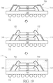
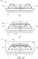
- FIG. 17 to FIG. 20 are schematic diagrams showing methods for forming package-on-package (PoP) according to various embodiments of the invention, wherein like numeral numbers designate like elements, regions, or layers.
- a bottom package 600 is provided.
- the bottom package 600 comprises a first semiconductor die 620 mounted on a substrate 610.
- a plurality of solder balls 611 may be mounted on a lower surface of the substrate 610.
- the first semiconductor die 620 may be encapsulated by a first molding compound 630.
- Through mold vias 640 may be provided in the first molding compound 630.
- the first semiconductor die 620 is electrically connected to the substrate 610 through bonding wires in the figures, it is understood that the semiconductor die 620 may be a flip chip in other embodiments.
- a printing process such as a screen printing process or a 3D printing process may be performed to print conductive traces 644 such as bonding fingers on the first molding compound 630.
- the printed conductive traces 644 are electrically connected to the through mold vias 640, respectively.
- the printed conductive traces 644 may be subjected to a curing process.
- a conductive layer such as Pt, Ag, or the like may be provided on the printed conductive traces 644.
- a second semiconductor die 650 is then mounted on the first molding compound 630.
- bonding wires 652 are formed to electrically connect the second semiconductor die 650 to the conductive traces 644.
- the second semiconductor die 650 may be encapsulated by a second molding compound 660, thereby forming a package-on-package 6.
- a bottom package 600 is provided.
- the bottom package 600 comprises a first semiconductor die 620 mounted on a substrate 610.
- a plurality of solder balls 611 may be mounted on a lower surface of the substrate 610.
- the first semiconductor die 620 may be encapsulated by a first molding compound 630.
- Through mold vias 640 may be provided in the first molding compound 630.
- first semiconductor die 620 is electrically connected to the substrate 610 through bonding wires in this figure, it is understood that the first semiconductor die 620 may be a flip chip in other embodiments.
- a printing process such as a screen printing process or a 3D printing process may be performed to print conductive traces 644 including bond pads 644a on the first molding compound 630.
- the printed conductive traces 644 are electrically connected to the through mold vias 640, respectively.
- the printed conductive traces 644 may be subjected to a curing process .
- a conductive layer such as Pt, Ag, or the like may be provided on the printed conductive traces 644.
- a second semiconductor die 650 is then bonded on the bond pads 644a in a flip chip configuration. Subsequently, the second semiconductor die 650 may be encapsulated by a second molding compound 660, thereby forming a package-on-package 6a.
- a bottom package 700 is provided.
- the bottom package 700 comprises a first semiconductor die 720 mounted on a substrate 710.
- a plurality of solder balls 711 may be mounted on a lower surface of the substrate 710.
- the first semiconductor die 720 may be encapsulated by a first molding compound 730.
- first semiconductor die 720 is electrically connected to the substrate 710 through bonding wires in this figure, it is understood that the first semiconductor die 720 may be a flip chip in other embodiments.
- a printing process such as a screen printing process or a 3D printing process may be performed to print conductive traces 740 such as bonding fingers on the top surface of the first molding compound 730.
- the conductive traces 740 may extend to the oblique sidewall of the first molding compound 730.
- the printed conductive traces 740 may be electrically connected to the conductive traces on or in the substrate 710.
- the printed conductive traces 740 may be subjected to a curing process.
- a conductive layer such as Pt, Ag, or the like may be provided on the printed conductive traces 740.
- a second semiconductor die 750 is then mounted on the first molding compound 730.
- bonding wires 752 are formed to electrically connect the semiconductor die 750 to the conductive traces 740.
- the second semiconductor die 750 may be encapsulated by a second molding compound 760, thereby forming a package-on-package 7.
- the bottom package 700 comprises a first semiconductor die 720 mounted on a substrate 710.
- a plurality of solder balls 711 may be mounted on a lower surface of the substrate 710.
- the first semiconductor die 720 may be encapsulated by a first molding compound 730.
- first semiconductor die 720 is electrically connected to the substrate 710 through bonding wires in this figure, it is understood that the first semiconductor die 720 may be a flip chip in other embodiments.
- a printing process such as a screen printing process or a 3D printing process may be performed to print conductive traces 740 including bond pads 740a on the top surface of the first molding compound 730.
- the conductive traces 740 may extend to the oblique sidewall of the first molding compound 730.
- the printed conductive traces 740 may be electrically connected to the conductive traces on the substrate 710.
- the printed conductive traces 740 may be subjected to a curing process.
- a conductive layer such as Pt, Ag, or the like may be provided on the printed conductive traces 740.
- a second semiconductor die 750 is then bonded on the bond pads 740a in a flip chip configuration. Subsequently, the second semiconductor die 750 may be encapsulated by a second molding compound 760, thereby forming a package-on-package 7a.
- FIG. 21 is a schematic diagram showing a semiconductor chip package according to another embodiment of the invention.
- the semiconductor chip package 8 comprises a semiconductor die 820 mounted on a substrate 810 such as a package substrate.
- a plurality of solder balls 811 may be mounted on a lower surface of the substrate 810.
- the semiconductor die 820 may be encapsulated by a molding compound 830.
- the semiconductor die 820 is electrically connected to the substrate 810 through bonding wires in this figure, it is understood that the semiconductor die 820 may be a flip chip in other embodiments.
- a plurality of heat-dissipating features 840 are embedded in the top surface of the molding compound 830.
- trenches are formed by laser marking laser in the top surface of the molding compound 830, conductive paste such as copper paste is then printed onto the top surface of the molding compound 830 and fills the trenches.
- the trenches formed in the top surface of the molding compound 830 are laser marking trenches and may comprise various patterns, letters or numbers so as to exhibit certain information such as trademarks or model.
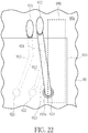
- FIG. 22 is a schematic top view partially showing a layout of a substrate according to another embodiment of the invention.
- the substrate may be a package substrate, a printed circuit board, or a printed wiring board.
- a plurality of conductive traces is formed on a top surface 90a of the substrate 90.
- the traces 911 and 912 are covered with a solder mask 910.
- the trace 911 interconnects a via 921 to a bonding finger 931 disposed outbound of the solder mask 910.
- the trace 912 may interconnect a via 922 to a via 924.
- the trace 912, the via 922, and the via 924 are covered with the solder mask 910.
- a solder mask opening 910a is formed in the solder mask 910 to expose a via 923.
- a conductive trace 913 is disposed over the solder mask 910 to electrically connect the bonding finger 932 to the via 923.
- the conductive trace 913 may be printed over the solder mask 910 by using a screen printing process or a 3D printing method.
- the conductive trace 913 may comprise conductive paste such as copper paste and may be subjected to a curing process. By providing such trace-over-solder mask configuration, a region 950 under the solder mask 910 may be spared so as to increase the routing flexibility of the substrate 90.
Landscapes
- Internal Circuitry In Semiconductor Integrated Circuit Devices (AREA)
- Die Bonding (AREA)
- Structures Or Materials For Encapsulating Or Coating Semiconductor Devices Or Solid State Devices (AREA)
Abstract
Description
- This application is a continuation-in-part of
U. S. application Ser. No. 15/063,433 filed March 7, 2016 , which itself claims the priority fromU. S. provisional application No. 62/161,591 filed May 14, 2015 U. S. provisional application No. 62/190, 401 filed July 9, 2015 U. S. provisional application No. 62/442,473 filed January 5, 2017 U. S. provisional application No. 62/445,278 filed January 12, 2017 - The present invention relates to interconnects of integrated circuits and semiconductor chip packages.
- An integrated circuit (IC) die is a small device formed on a semiconductor wafer, such as a silicon wafer. Such a die is typically cut from the wafer and attached to a substrate for interconnect redistribution. Bond pads on the die are then electrically connected to the leads on the carrier via wire bonding. The die and the bonding wires are then encapsulated with a molding compound such that a package is formed.
- Typically, the leads encapsulated in the package are redistributed in a network of conductors within the carrier and end in an array of terminal points outside the package. Manufacturers have been stacking two or more die within a single package. Such devices are sometimes referred to as stacked multichip packages.
- One stacked multichip package is generally illustrated in
FIG. 1 . In this configuration afirst die 11 is mounted on asubstrate 10. Asecond die 12 may then be adhesively secured to the top surface of thefirst die 11 thereby creating a stacked die configuration. Thesecond die 12 partially overlaps with thefirst die 11 when viewed from the above.Bonding wires first die 11 and thesecond die 12 to the respective bond fingers on thesubstrate 10 using conventional wire bonder. Anencapsulant material 20 is molded over thesubstrate 10 to provide an encapsulant cap. - As known in the art, a stand-off stitch bonding process typically comprises placing a flat-topped bump on an active integrated circuit (IC) pad such as an aluminum pad, and then reverse bonding from the substrate or package back to the flat-topped ball bump. However, it is difficult to form the
wire bond 18 on the bond pads of thesecond die 12 adjacent to the overhangingside edge 12a. The stress incurred by the wire bonder may cause peeling between thefirst die 11 and thesecond die 12 and reduce the production yield. - It is one objective of the claimed invention to provide an improved semiconductor chip package and a fabrication method thereof in order to solve the above-mentioned prior art problems.
- According to one aspect of the invention, a semiconductor chip package is defined in
independent claim 1, which includes a substrate; a semiconductor die mounted on the substrate, wherein the semiconductor die comprises a bond pad disposed on an active surface of the semiconductor die, and a passivation layer covering perimeter of the bond pad, wherein a bond pad opening in the passivation layer exposes a central area of the bond pad; a conductive paste post printed on the exposed central area of the bond pad; and a bonding wire secured to a top surface of the conductive paste post. The conductive paste post preferably comprises copper paste. - According to another aspect of the invention, a semiconductor chip package is defined in
independent claim 6, which includes a substrate; a semiconductor die mounted on the substrate, wherein the semiconductor die comprises a bond pad disposed on an active surface of the semiconductor die, and a passivation layer covering perimeter of the bond pad, wherein a bond pad opening in the passivation layer exposes a central area of the bond pad; a conductive paste post printed on the exposed central area of the bond pad; a conductive trace printed on the passivation layer and being electrically connected to the conductive paste post; a redistributed bond pad printed on the passivation layer, wherein the redistributed bond pad is electrically connected to the conductive paste post through the conductive trace; and a bonding wire secured to a top surface of the redistributed bond pad. - According to still another aspect of the invention, a method for forming a substrate is disclosed. A carrier is provided. A solder mask is coated on the carrier. The solder mask is patterned, thereby forming a plurality of openings in the solder mask. A first conductive paste is printed into the openings, thereby forming a first circuit layer. A dielectric layer is coated on the first circuit layer. The dielectric layer is patterned, thereby forming via openings in the dielectric layer. A second conductive paste is printed into the via openings and on the dielectric layer, thereby forming a second circuit layer.
- According to still another aspect of the invention, a package-on-package is disclosed and defined in
independent claim 10. The package-on-package includes a bottom package comprising a first semiconductor die mounted on a substrate, and a plurality of solder balls mounted on a lower surface of the substrate. The first semiconductor die is encapsulated by a first molding compound. Conductive traces are printed on the first molding compound. A second semiconductor die is mounted on the first molding compound. - According to still another aspect of the invention, a semiconductor chip package includes a semiconductor die mounted on a substrate; a plurality of solder balls mounted on a lower surface of the substrate; a molding compound encapsulating the semiconductor die; and a plurality of heat-dissipating features embedded in the top surface of the molding compound. The heat-dissipating features are composed of conductive paste.
- According to still another aspect of the invention, a substrate includes a plurality of conductive traces is formed on a top surface of the substrate; a solder mask covering the plurality of conductive traces; a bonding finger disposed outbound of the solder mask; a solder mask opening in the solder mask to expose a via in the substrate; and a conductive trace printed over the solder mask to electrically connect the bonding finger to the via.
- These and other objectives of the present invention will no doubt become obvious to those of ordinary skill in the art after reading the following detailed description of the preferred embodiment that is illustrated in the various figures and drawings.
- The accompanying drawings are included to provide a further understanding of the invention, and are incorporated in and constitute a part of this specification. The drawings illustrate embodiments of the invention and, together with the description, serve to explain the principles of the invention. In the drawings:
-
FIG. 1 is a schematic, cross-sectional diagram showing a conventional stacked multichip package; -
FIG. 2 to FIG. 4 are schematic, cross-sectional diagrams showing a conductive paste post on a bond pad for stand-off stitch bonding process in accordance with one embodiment of the invention; -
FIG. 5 andFIG. 6 show exemplary semiconductor chip packages incorporating the conductive paste post as depicted inFIG. 4 ; -
FIG. 7 to FIG. 10 are schematic, cross-sectional diagrams showing various embodiments in accordance with the present invention; -
FIG. 11 to FIG. 14 are schematic, cross-sectional diagrams showing a method for forming a substrate in accordance with one embodiment of the invention; -
FIG. 15 is a schematic diagram showing a tape automated bonding (TAB) method for fabricating a semiconductor chip package in accordance with one embodiment of the invention; -
FIG. 16 is a schematic diagram showing the processing of the semiconductor chip package fabricated inFIG. 15 ; -
FIG. 17 to FIG. 20 are schematic diagrams showing methods for forming package-on-package (PoP) according to various embodiments of the invention; -
FIG. 21 is a schematic diagram showing a semiconductor chip package according to another embodiment of the invention; and -
FIG. 22 is a schematic top view partially showing a layout of a substrate according to another embodiment of the invention. - In the following detailed description of embodiments of the invention, reference is made to the accompanying drawings, which form a part hereof, and in which is shown by way of illustration specific preferred embodiments in which the disclosure may be practiced.
- These embodiments are described in sufficient detail to enable those skilled in the art to practice them, and it is to be understood that other embodiments may be utilized and that mechanical, chemical, electrical, and procedural changes may be made without departing from the spirit and scope of the present disclosure. The following detailed description is, therefore, not to be taken in a limiting sense, and the scope of embodiments of the present invention is defined only by the appended claims.
- Please refer to
FIG. 2 to FIG .4. FIG. 2 to FIG. 4 are schematic, cross-sectional diagrams showing a conductive paste post on a bond pad for stand-off stitch bonding process in accordance with one embodiment of the invention. As shown inFIG. 2 and FIG. 3 , asemiconductor die 120 having abond pad 122 formed thereon is provided. Although only onebond pad 122 is illustrated in this figure, it is understood that the semiconductor die 120 may comprise a plurality of bond pads distributed on the active surface of the semiconductor die 120. For example, thebond pad 122 may be an aluminum bond pad. - Preferably, a
passivation layer 124 such as a polyimide layer may be formed on the semiconductor die 120 and cover the perimeter of thebond pad 122. Preferably, abond pad opening 124a in thepassivation layer 124 exposes a central area of thebond pad 122. - Preferably, a
conductive paste post 130 is printed on the exposed central area of thebond pad 122. For example, theconductive paste post 130 may comprise copper paste, but is not limited thereto. Theconductive paste post 130 may be formed by using screen-printing processes. Alternatively, theconductive paste post 130 may be formed by using 3D printing processes. Theconductive paste post 130 functions as a buffer to prevent aluminum extrusion. - Compared to the conventional flat-topped ball bump formed during a conventional stand-off stitch bonding process, the
conductive paste post 130 has a flattertop surface 130a. The flattertop surface 130a of theconductive paste post 130 provides higher reliability and better performance of the package devices. - Preferably, for example, the copper paste may comprise epoxy resin such as a thermosetting epoxy resin, and copper powder or silver-coated copper balls as filler, but is not limited thereto. After printing the
conductive paste post 130 on thebond pad 122, theconductive paste post 130 may be subjected to a curing process. Preferably, theconductive paste post 130 may be cured by thermal processes or ultraviolet (UV) light. - Optionally, the
top surface 130a of theconductive paste post 130 may be subjected to an etching process to expose more metal filler, thereby reducing the contact resistance. Preferably, aconductive layer 131 having low resistance, for example, Pt or Au, may be coated on thetop surface 130a of theconductive paste post 130. - The
conductive paste post 130 may completely fill up thebond pad opening 124a, as shown inFIG. 2 . InFIG. 2 , the peripheral sidewall of theconductive paste post 130 is in direct contact with thepassivation layer 124. Alternatively, theconductive paste post 130 does not completely fill up thebond pad opening 124a, as shown inFIG. 3 . InFIG. 3 , the peripheral sidewall of theconductive paste post 130 is not in direct contact with thepassivation layer 124. Agap 132 may be formed between the peripheral sidewall of theconductive paste post 130 and thepassivation layer 124. -
FIG. 4 shows theconductive paste post 130 after a bonding wire is bonded thereon. As shown inFIG. 4 , a wire bonding process such as a stand-off stitch bonding process may be performed to secure abonding wire 180 on thetop surface 130a of theconductive paste post 130. Preferably, theconductive paste post 130 replaces the conventional flat-topped ball bump formed during a conventional stand-off stitch bonding process. Further, theconductive paste post 130 may be printed on the semiconductor die 120 prior to the wire bonding process. Therefore, the stress exerted on the overhanging side edge of the top die as depicted inFIG. 1 may be reduced or avoided. The throughput (UPH or unit per hour) of the wire bonding process is also improved. - Because of the resilient property of the
conductive paste post 130, theconductive paste post 130 quickly recovers its shape after thebonding wire 180 is formed. The shorting between the adjacent bond pads may be avoided. Therefore, smaller bond pad opening and bond pad pitch may be employed. -
FIG. 5 shows an exemplarysemiconductor chip package 1 incorporating the conductive paste post as depicted inFIG. 4 , wherein like numeral numbers designate like elements, regions, or layers. As shown inFIG. 5 , thesemiconductor chip package 1 comprises asecond die 120 mounted on afirst die 110. Thesecond die 120 is adhesively secured to the top surface of thefirst die 110 thereby creating a stacked die configuration. Thesecond die 120 partially overlaps with thefirst die 110 when viewed from the above. Anencapsulant material 200 such as an epoxy molding compound is molded over thesubstrate 100 to provide an encapsulant cap. -
Bonding wires first die 110 and thesecond die 120 to therespective bond fingers substrate 100 using a wire bonder. Thesubstrate 100 may be a package substrate, but is not limited thereto. Thebonding wire 180 may be secured to thebond finger 104 on thesubstrate 100 and then reverse bonded to theconductive paste post 130 on thesecond die 120. -
FIG. 6 shows an exemplarysemiconductor chip package 2 incorporating the conductive paste post as depicted inFIG. 4 , wherein like numeral numbers designate like elements, regions, or layers. As shown inFIG. 6 , thesemiconductor chip package 2 comprises asingle die 120 mounted on thesubstrate 100.Bonding wires 180 are formed to electrically connect thedie 120 to therespective bond fingers 104 on thesubstrate 100 using a wire bonder. Thesubstrate 100 may be a package substrate, but is not limited thereto. Thebonding wire 180 may be secured to thebond finger 104 on thesubstrate 100 and then reverse bonded to theconductive paste post 130 on thedie 120. - It is understood that the package structures shown in
FIG. 5 andFIG. 6 are for illustration purposes only. Other package structures may be employed without departing from the spirit or scope of the present invention. - Please refer to
FIG. 7 to FIG. 10. FIG. 7 to FIG. 10 are schematic, cross-sectional diagrams showing various embodiments in accordance with the present invention, wherein like numeral numbers designate like elements, regions, or layers. The redistribution layer (RDL) structures shown inFIG. 7 to FIG. 10 may be applicable to the semiconductor chip packages as set forth inFIG. 5 andFIG. 6 . - As shown in
FIG. 7 , likewise, asemiconductor die 120 having abond pad 122 formed thereon is provided. Although only onebond pad 122 is illustrated in this figure, it is understood that the semiconductor die 120 may comprise a plurality of bond pads distributed on the active surface of the semiconductor die 120. For example, thebond pad 122 may be an aluminum bond pad. - Preferably, a
passivation layer 124 such as a polyimide layer may be formed on the semiconductor die 120 and cover the perimeter of thebond pad 122. Preferably, abond pad opening 124a in thepassivation layer 124 exposes a central area of thebond pad 122. - Preferably, a
conductive paste post 130 is printed on the exposed central area of thebond pad 122. For example, theconductive paste post 130 may comprise copper paste, but is not limited thereto. Theconductive paste post 130 may be formed by using screen-printing processes. Alternatively, theconductive paste post 130 may be formed by using 3D printing processes. - Preferably, a
conductive trace 136 is printed on thepassivation layer 124. Theconductive trace 136 is electrically connected to theconductive paste post 130. Theconductive trace 136 may comprise copper paste, but is not limited thereto. Preferably, theconductive paste post 130 and theconductive trace 136 may be printed by using the same printing process. - Preferably, a redistributed
bond pad 138 is also printed on thepassivation layer 124. The redistributedbond pad 138 is electrically connected to theconductive paste post 130 through theconductive trace 136. The redistributedbond pad 138 is thicker than theconductive trace 136. - The
conductive paste post 130, theconductive trace 136, and the redistributedbond pad 138 may be printed by using the same printing process, and may be subjected to a curing process. Theconductive paste post 130 is structurally integral with theconductive trace 136 and the redistributedbond pad 138. Theconductive paste post 130, theconductive trace 136, and the redistributedbond pad 138 constitute aredistribution layer structure 300. - As shown in
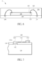
FIG. 8 , asemiconductor die 120 having abond pad 122 formed thereon is provided. Although only onebond pad 122 is illustrated in this figure, it is understood that the semiconductor die 120 may comprise a plurality of bond pads distributed on the active surface of the semiconductor die 120. For example, thebond pad 122 may be an aluminum bond pad. - Preferably, a
passivation layer 124 such as a polyimide layer may be formed on the semiconductor die 120 and cover the perimeter of thebond pad 122. Preferably, thebond pad opening 124a exposes a central area of thebond pad 122. - Likewise, a
conductive paste post 130, aconductive trace 136, and a redistributedbond pad 138 are printed onto the semiconductor die 120 as described inFIG. 7 . An insulatinglayer 140 may be formed on the semiconductor die 120. Preferably, the insulatinglayer 140 may comprise a molding compound, but is not limited thereto. The insulatinglayer 140 covers theconductive paste post 130, theconductive trace 136, and the redistributedbond pad 138. Anopening 140a may be formed in the insulatinglayer 140 to partially expose the redistributedbond pad 138. Abonding wire 180 may be secured to the exposed redistributedbond pad 138. - As shown in
FIG. 9 , asemiconductor die 120 having abond pad 122 formed thereon is provided. Although only onebond pad 122 is illustrated in this figure, it is understood that the semiconductor die 120 may comprise a plurality of bond pads distributed on the active surface of the semiconductor die 120. For example, thebond pad 122 may be an aluminum bond pad. - Preferably, a
passivation layer 124 such as a polyimide layer may be formed on the semiconductor die 120 and cover the perimeter of thebond pad 122. Preferably, thebond pad opening 124a exposes a central area of thebond pad 122. - A
conductive paste post 130, aconductive trace 136, and a redistributedbond pad 138 are printed onto the semiconductor die 120 as described inFIG. 7 . An insulatinglayer 140 may be formed on the semiconductor die 120. Preferably, the insulatinglayer 140 may comprise a molding compound, but is not limited thereto. The insulatinglayer 140 covers theconductive paste post 130, theconductive trace 136, and the redistributedbond pad 138. The insulatinglayer 140 is subjected to a polishing process to expose the redistributedbond pad 138. Abonding wire 180 may be secured to the exposed redistributedbond pad 138. - As shown in
FIG. 10 , the difference between the structure ofFIG. 10 and thestructure 2 ofFIG. 8 is that the structure ofFIG. 10 further comprises a printedpassive element 150 on thepassivation layer 124. Preferably, thepassive element 150 may comprise copper paste as the composition used to form theconductive paste post 130, theconductive trace 136, and the redistributedbond pad 138. Thepassive element 150 may be a resistor, a capacitor, or an inductor, but is not limited thereto. - Please refer to
FIG. 11 to FIG. 14. FIG. 11 to FIG. 14 are schematic, cross-sectional diagrams showing a method for forming asubstrate 400 in accordance with one embodiment of the invention. Thesubstrate 400 may be an interposer substrate, a package substrate, or a circuit board. - As shown in
FIG. 11 , a layer ofsolder mask 420 is coated on acarrier 410. Subsequently, thesolder mask 420 may be patterned by using a lithographic process, thereby forming a plurality ofopenings 420a. Preferably, thecarrier 410 may be a plastic substrate or a flexible substrate, but is not limited thereto. - As shown in
FIG. 12 , a printing process is performed to print a conductive paste such as copper paste into theopenings 420a, thereby forming afirst circuit layer 430. Preferably, for example, thefirst circuit layer 430 may comprise ball grid array (BGA) ball pads and interconnect traces. Preferably, the printing process may comprise screen-printing process, but is not limited thereto. Thefirst circuit layer 430 may be subjected to a curing process. - As shown in
FIG. 13 , adielectric layer 440 is then coated on thefirst circuit layer 430. Preferably, thedielectric layer 440 may comprise polyimide, ABF (Ajinomoto Buildup Film) or the like, but is not limited thereto. A lithographic process may be performed to pattern thedielectric layer 440, thereby forming viaopenings 440a in thedielectric layer 440. The viaopenings 440a partially expose thefirst circuit layer 430 respectively. - As shown in
FIG. 14 , a printing process is performed to print a conductive paste such as copper paste into the viaopenings 440a and on thedielectric layer 440, thereby forming asecond circuit layer 450. Thesecond circuit layer 450 comprises viaelements 450a for electrically connecting thesecond circuit layer 450 to thefirst circuit layer 430. It is understood that the steps as depicted throughFIG. 11 to FIG. 14 may be repeated to form a desired number of interconnect layers in the interposer substrate. - Please refer to
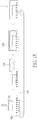
FIG. 15. FIG. 15 is a schematic diagram showing a tape automated bonding (TAB) method for fabricating a semiconductor chip package in accordance with one embodiment of the invention.FIG. 16 is a schematic diagram showing the processing of the semiconductor chip package fabricated inFIG. 15 . - As shown in
FIG. 15 , thesubstrate 400 such as an interposer substrate or a package substrate may be pre-fabricated on theTAB tape 510, for example, by the steps depicted throughFIG. 11 to FIG. 14 . TheTAB tape 510 may be composed of polyimide, but is not limited thereto. At the first station, aflip chip 520 such as a solder bumped chip or die may be bonded on thesubstrate 400. - After the chip placement and bonding, the chip assembly is then subjected to a curing and solder reflow process at the second station to cure the copper paste of the
substrate 400 and reflow the solder joints between theflip chip 520 and thesubstrate 400. For example, an infrared (IR)reflow device 530 may be used during the curing process, but is not limited thereto. - Thereafter, a molding process is performed at the third station. A
molding compound 540 is applied. Themolding compound 540 covers the attachedflip chip 520 and the and the top surface of thesubstrate 400. Themolding compound 540 may be subjected to a curing process. Themolding compound 540 may comprise a mixture of epoxy and silica fillers, but not limited thereto. After the molding process, thesemiconductor chip package 5 is detached from theTAB tape 510. - As shown in
FIG. 16 , after the detachment of thesemiconductor chip package 5 from theTAB tape 510, the exposed lower surfaces (ball pads) of thefirst circuit layer 430 may be covered with asurface finish layer 460 such as a Ni/Au layer or a ASOP layer. Subsequently, connection elements such as ball grid array (BGA) balls (not shown) may be formed on the ball pads. -
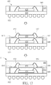
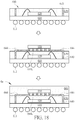
FIG. 17 to FIG. 20 are schematic diagrams showing methods for forming package-on-package (PoP) according to various embodiments of the invention, wherein like numeral numbers designate like elements, regions, or layers. - As shown in
FIG. 17 , abottom package 600 is provided. Thebottom package 600 comprises a first semiconductor die 620 mounted on asubstrate 610. A plurality ofsolder balls 611 may be mounted on a lower surface of thesubstrate 610. The first semiconductor die 620 may be encapsulated by afirst molding compound 630. Through mold vias 640 may be provided in thefirst molding compound 630. - Although the first semiconductor die 620 is electrically connected to the
substrate 610 through bonding wires in the figures, it is understood that the semiconductor die 620 may be a flip chip in other embodiments. - Subsequently, a printing process such as a screen printing process or a 3D printing process may be performed to print
conductive traces 644 such as bonding fingers on thefirst molding compound 630. The printedconductive traces 644 are electrically connected to the throughmold vias 640, respectively. After the printing process, the printedconductive traces 644 may be subjected to a curing process. Optionally, a conductive layer such as Pt, Ag, or the like may be provided on the printed conductive traces 644. - A second semiconductor die 650 is then mounted on the
first molding compound 630. Preferably,bonding wires 652 are formed to electrically connect the second semiconductor die 650 to the conductive traces 644. Subsequently, the second semiconductor die 650 may be encapsulated by asecond molding compound 660, thereby forming a package-on-package 6. - As shown in
FIG. 18 , likewise, abottom package 600 is provided. Thebottom package 600 comprises a first semiconductor die 620 mounted on asubstrate 610. A plurality ofsolder balls 611 may be mounted on a lower surface of thesubstrate 610. The first semiconductor die 620 may be encapsulated by afirst molding compound 630. Through mold vias 640 may be provided in thefirst molding compound 630. - Although the first semiconductor die 620 is electrically connected to the
substrate 610 through bonding wires in this figure, it is understood that the first semiconductor die 620 may be a flip chip in other embodiments. - Subsequently, a printing process such as a screen printing process or a 3D printing process may be performed to print
conductive traces 644 including bond pads 644a on thefirst molding compound 630. The printedconductive traces 644 are electrically connected to the throughmold vias 640, respectively. After the printing process, the printedconductive traces 644 may be subjected to a curing process . Optionally, a conductive layer such as Pt, Ag, or the like may be provided on the printed conductive traces 644. - A second semiconductor die 650 is then bonded on the bond pads 644a in a flip chip configuration. Subsequently, the second semiconductor die 650 may be encapsulated by a
second molding compound 660, thereby forming a package-on-package 6a. - As shown in
FIG. 19 , abottom package 700 is provided. Thebottom package 700 comprises a first semiconductor die 720 mounted on asubstrate 710. A plurality ofsolder balls 711 may be mounted on a lower surface of thesubstrate 710. The first semiconductor die 720 may be encapsulated by afirst molding compound 730. - Although the first semiconductor die 720 is electrically connected to the
substrate 710 through bonding wires in this figure, it is understood that the first semiconductor die 720 may be a flip chip in other embodiments. - Subsequently, a printing process such as a screen printing process or a 3D printing process may be performed to print
conductive traces 740 such as bonding fingers on the top surface of thefirst molding compound 730. The conductive traces 740 may extend to the oblique sidewall of thefirst molding compound 730. The printedconductive traces 740 may be electrically connected to the conductive traces on or in thesubstrate 710. After the printing process, the printedconductive traces 740 may be subjected to a curing process. Optionally, a conductive layer such as Pt, Ag, or the like may be provided on the printed conductive traces 740. - A second semiconductor die 750 is then mounted on the
first molding compound 730. Preferably,bonding wires 752 are formed to electrically connect the semiconductor die 750 to the conductive traces 740. Subsequently, the second semiconductor die 750 may be encapsulated by asecond molding compound 760, thereby forming a package-on-package 7. - As shown in
FIG. 20 , likewise, abottom package 700 is provided. Thebottom package 700 comprises a first semiconductor die 720 mounted on asubstrate 710. A plurality ofsolder balls 711 may be mounted on a lower surface of thesubstrate 710. The first semiconductor die 720 may be encapsulated by afirst molding compound 730. - Although the first semiconductor die 720 is electrically connected to the
substrate 710 through bonding wires in this figure, it is understood that the first semiconductor die 720 may be a flip chip in other embodiments. - Subsequently, a printing process such as a screen printing process or a 3D printing process may be performed to print
conductive traces 740 includingbond pads 740a on the top surface of thefirst molding compound 730. The conductive traces 740 may extend to the oblique sidewall of thefirst molding compound 730. The printedconductive traces 740 may be electrically connected to the conductive traces on thesubstrate 710. After the printing process, the printedconductive traces 740 may be subjected to a curing process. Optionally, a conductive layer such as Pt, Ag, or the like may be provided on the printed conductive traces 740. - A second semiconductor die 750 is then bonded on the
bond pads 740a in a flip chip configuration. Subsequently, the second semiconductor die 750 may be encapsulated by asecond molding compound 760, thereby forming a package-on-package 7a. - Please refer to
FIG. 21. FIG. 21 is a schematic diagram showing a semiconductor chip package according to another embodiment of the invention. As shown inFIG. 21 , the semiconductor chip package 8 comprises asemiconductor die 820 mounted on asubstrate 810 such as a package substrate. A plurality ofsolder balls 811 may be mounted on a lower surface of thesubstrate 810. The semiconductor die 820 may be encapsulated by amolding compound 830. - Although the semiconductor die 820 is electrically connected to the
substrate 810 through bonding wires in this figure, it is understood that the semiconductor die 820 may be a flip chip in other embodiments. - A plurality of heat-dissipating
features 840 are embedded in the top surface of themolding compound 830. To form the heat-dissipatingfeatures 840, first, trenches are formed by laser marking laser in the top surface of themolding compound 830, conductive paste such as copper paste is then printed onto the top surface of themolding compound 830 and fills the trenches. The trenches formed in the top surface of themolding compound 830 are laser marking trenches and may comprise various patterns, letters or numbers so as to exhibit certain information such as trademarks or model. -
FIG. 22 is a schematic top view partially showing a layout of a substrate according to another embodiment of the invention. The substrate may be a package substrate, a printed circuit board, or a printed wiring board. - As shown in
FIG. 22 , a plurality of conductive traces is formed on atop surface 90a of thesubstrate 90. For the sake of simplicity, only twotraces traces solder mask 910. For example, thetrace 911 interconnects a via 921 to abonding finger 931 disposed outbound of thesolder mask 910. Thetrace 912 may interconnect a via 922 to a via 924. In this embodiment, thetrace 912, the via 922, and the via 924 are covered with thesolder mask 910. Asolder mask opening 910a is formed in thesolder mask 910 to expose a via 923. - A
conductive trace 913 is disposed over thesolder mask 910 to electrically connect thebonding finger 932 to thevia 923. Theconductive trace 913 may be printed over thesolder mask 910 by using a screen printing process or a 3D printing method. Theconductive trace 913 may comprise conductive paste such as copper paste and may be subjected to a curing process. By providing such trace-over-solder mask configuration, aregion 950 under thesolder mask 910 may be spared so as to increase the routing flexibility of thesubstrate 90. - Those skilled in the art will readily observe that numerous modifications and alterations of the device and method may be made while retaining the teachings of the invention. Accordingly, the above disclosure should be construed as limited only by the metes and bounds of the appended claims.
Claims (15)
- A semiconductor chip package (1; 2), comprising:a substrate (100);a semiconductor die (120) mounted on the substrate (100), wherein the semiconductor die (120) comprises a bond pad (122) disposed on an active surface of the semiconductor die (120), and a passivation layer (124) covering perimeter of the bond pad (122), wherein a bond pad opening (124a) in the passivation layer (124) exposes a central area of the bond pad (122);a conductive paste post (130) printed on the exposed central area of the bond pad (122); anda bonding wire (180) secured to a top surface (130a) of the conductive paste post (130).
- The semiconductor chip package according to claim 1, wherein the conductive paste post (130) comprises copper paste
wherein preferably the copper paste comprises epoxy resin and copper powder or silver-coated copper balls as filler. - The semiconductor chip package according to claim 1 or 2, wherein the conductive paste post (130) completely fills up the bond pad opening (124a), wherein a peripheral sidewall of the conductive paste post (130) is in direct contact with the passivation layer (124), or
wherein the conductive paste post (130) does not completely fill up the bond pad opening (124a), wherein a peripheral sidewall of the conductive paste post (130) is not in direct contact with the passivation layer (124). - The semiconductor chip package according to any one of claims 1 to 3 further comprising a conductive layer coated on the top surface of the conductive paste post (130), and/or
further comprising an encapsulant material molded over the substrate. - The semiconductor chip package according to any one of claims 1 to 4, wherein the passivation layer (124) comprises a polyimide layer, and/or
wherein the bond pad (122) is an aluminum bond pad. - A semiconductor chip package, comprising:a substrate;a semiconductor die (120) mounted on the substrate, wherein the semiconductor die (120) comprises a bond pad (122) disposed on an active surface of the semiconductor die (120) , and a passivation layer (124) covering perimeter of the bond pad (122), wherein a bond pad opening (124a) in the passivation layer (124) exposes a central area of the bond pad (122);a conductive paste post (130) printed on the exposed central area of the bond pad (122);a conductive trace (136) printed on the passivation layer (124) and being electrically connected to the conductive paste post (130);a redistributed bond pad (138) printed on the passivation layer (124), wherein the redistributed bond pad (138) is electrically connected to the conductive paste post (130) through the conductive trace (136); anda bonding wire (180) secured to a top surface of the redistributed bond pad (138).
- The semiconductor chip package according to claim 6, wherein the conductive paste post (130) is structurally integral with the conductive trace (136) and the redistributed bond pad (138).
- The semiconductor chip package according to claim 6 or 7, further comprising an insulating layer (140) on the passivation layer (124), and wherein the insulating layer (140) covers the conductive paste post (130), the conductive trace (136), and the redistributed bond pad (138) , and wherein the insulating layer (140) comprises an opening (140a) exposing the redistributed bond pad (138),
wherein preferably the insulating layer comprises a molding compound. - The semiconductor chip package according to any one of claims 6 to 8 further comprising a passive element printed on the passivation layer (124).
- A package-on-package (6), comprising:a bottom package (600) comprising a first semiconductor die (620) mounted on a substrate (610), and a plurality of solder balls (611) mounted on a lower surface of the substrate (610), wherein the first semiconductor die (620) is encapsulated by a first molding compound (630);conductive traces (644) printed on the first molding compound (630); anda second semiconductor die (650) mounted on the first molding compound (630).
- The package-on-package according to claim 10, wherein the first semiconductor die (620) is electrically connected to the substrate (610) through bonding wires, and/or
wherein the first semiconductor die (620) is a flip chip. - The package-on-package according to claim 10 or 11, wherein the conductive traces (644) comprise bonding fingers,
and preferably further comprising bonding wires (652) electrically connecting the second semiconductor die (650) to the bonding fingers. - The package-on-package according to any one of claims 10 to 12, further comprising a second molding compound (660) encapsulating the second semiconductor die (650).
- The package-on-package according to any one of claims 10 to 13, wherein the conductive traces (644) comprise bond pads (644a) on the first molding compound (630).
- The package-on-package according to any one of claims 10 to 14, further comprising through mold vias (640) in the first molding compound (630),
wherein preferably the conductive traces (644) are electrically connected to the through mold vias (640), respectively.
Applications Claiming Priority (3)
| Application Number | Priority Date | Filing Date | Title |
|---|---|---|---|
| US201762442473P | 2017-01-05 | 2017-01-05 | |
| US201762445278P | 2017-01-12 | 2017-01-12 | |
| US15/701,456 US10685943B2 (en) | 2015-05-14 | 2017-09-12 | Semiconductor chip package with resilient conductive paste post and fabrication method thereof |
Publications (2)
| Publication Number | Publication Date |
|---|---|
| EP3346492A2 true EP3346492A2 (en) | 2018-07-11 |
| EP3346492A3 EP3346492A3 (en) | 2018-08-08 |
Family
ID=60162119
Family Applications (1)
| Application Number | Title | Priority Date | Filing Date |
|---|---|---|---|
| EP17197972.7A Withdrawn EP3346492A3 (en) | 2017-01-05 | 2017-10-24 | Semiconductor chip package and fabrication method thereof |
Country Status (3)
| Country | Link |
|---|---|
| EP (1) | EP3346492A3 (en) |
| CN (1) | CN108281408A (en) |
| TW (1) | TW201826477A (en) |
Cited By (3)
| Publication number | Priority date | Publication date | Assignee | Title |
|---|---|---|---|---|
| US10685943B2 (en) | 2015-05-14 | 2020-06-16 | Mediatek Inc. | Semiconductor chip package with resilient conductive paste post and fabrication method thereof |
| US11444019B2 (en) | 2020-04-06 | 2022-09-13 | Qualcomm Incorporated | Package comprising a substrate with interconnect routing over solder resist layer and an integrated device coupled to the substrate and method for manufacturing the package |
| EP4322213A1 (en) * | 2022-08-08 | 2024-02-14 | Azurewave Technologies, Inc. | Chip package structure and package module thereof |
Families Citing this family (7)
| Publication number | Priority date | Publication date | Assignee | Title |
|---|---|---|---|---|
| CN109872982A (en) * | 2019-03-08 | 2019-06-11 | 东莞记忆存储科技有限公司 | Semiconductor multilayer crystal grain stacking module and welding method thereof |
| CN112151463B (en) * | 2019-06-28 | 2026-01-09 | 意法半导体公司 | Semiconductor packages with cavities in the die pads used to reduce voids in the solder. |
| KR102685892B1 (en) * | 2019-08-20 | 2024-07-19 | 에스케이하이닉스 주식회사 | Semiconductor package including stacked semiconductor chips |
| US10978419B1 (en) * | 2019-10-14 | 2021-04-13 | Nanya Technology Corporation | Semiconductor package and manufacturing method thereof |
| US11296065B2 (en) * | 2020-06-15 | 2022-04-05 | Taiwan Semiconductor Manufacturing Co., Ltd. | Semiconductor packages and methods of forming same |
| TWI822016B (en) * | 2022-04-28 | 2023-11-11 | 元太科技工業股份有限公司 | Display device |
| US12525161B2 (en) | 2022-04-28 | 2026-01-13 | E Ink Holdings Inc. | Narrow border reflective display device |
Family Cites Families (10)
| Publication number | Priority date | Publication date | Assignee | Title |
|---|---|---|---|---|
| JPH0252443A (en) * | 1988-08-17 | 1990-02-22 | Mitsubishi Electric Corp | Wire bonding |
| JPH08107123A (en) * | 1994-10-04 | 1996-04-23 | Hitachi Ltd | Method of manufacturing semiconductor integrated circuit device, manufacturing apparatus thereof, and semiconductor integrated circuit device |
| US7633765B1 (en) * | 2004-03-23 | 2009-12-15 | Amkor Technology, Inc. | Semiconductor package including a top-surface metal layer for implementing circuit features |
| US7176580B1 (en) * | 2003-10-24 | 2007-02-13 | Joseph Fjelstad | Structures and methods for wire bonding over active, brittle and low K dielectric areas of an IC chip |
| JP5123633B2 (en) * | 2007-10-10 | 2013-01-23 | ルネサスエレクトロニクス株式会社 | Semiconductor devices and connecting materials |
| KR20100124161A (en) * | 2009-05-18 | 2010-11-26 | 주식회사 하이닉스반도체 | Fabricating method for semiconductor package |
| US20120228768A1 (en) * | 2011-03-07 | 2012-09-13 | Reza Argenty Pagaila | Integrated circuit packaging system using b-stage polymer and method of manufacture thereof |
| KR20140064053A (en) * | 2012-11-19 | 2014-05-28 | 삼성전자주식회사 | Semiconductor package having redistribution layer |
| JP6122290B2 (en) * | 2011-12-22 | 2017-04-26 | 三星電子株式会社Samsung Electronics Co.,Ltd. | Semiconductor package having a rewiring layer |
| JP6437246B2 (en) * | 2014-08-28 | 2018-12-12 | ルネサスエレクトロニクス株式会社 | Semiconductor device and manufacturing method thereof |
-
2017
- 2017-10-24 EP EP17197972.7A patent/EP3346492A3/en not_active Withdrawn
- 2017-12-08 CN CN201711303574.6A patent/CN108281408A/en not_active Withdrawn
- 2017-12-11 TW TW106143338A patent/TW201826477A/en unknown
Non-Patent Citations (1)
| Title |
|---|
| None |
Cited By (3)
| Publication number | Priority date | Publication date | Assignee | Title |
|---|---|---|---|---|
| US10685943B2 (en) | 2015-05-14 | 2020-06-16 | Mediatek Inc. | Semiconductor chip package with resilient conductive paste post and fabrication method thereof |
| US11444019B2 (en) | 2020-04-06 | 2022-09-13 | Qualcomm Incorporated | Package comprising a substrate with interconnect routing over solder resist layer and an integrated device coupled to the substrate and method for manufacturing the package |
| EP4322213A1 (en) * | 2022-08-08 | 2024-02-14 | Azurewave Technologies, Inc. | Chip package structure and package module thereof |
Also Published As
| Publication number | Publication date |
|---|---|
| EP3346492A3 (en) | 2018-08-08 |
| CN108281408A (en) | 2018-07-13 |
| TW201826477A (en) | 2018-07-16 |
Similar Documents
| Publication | Publication Date | Title |
|---|---|---|
| US9165878B2 (en) | Semiconductor packages and methods of packaging semiconductor devices | |
| US10685943B2 (en) | Semiconductor chip package with resilient conductive paste post and fabrication method thereof | |
| US10128211B2 (en) | Thin fan-out multi-chip stacked package structure and manufacturing method thereof | |
| US10276553B2 (en) | Chip package structure and manufacturing method thereof | |
| JP5661225B2 (en) | Semiconductor device packaging method | |
| US6518089B2 (en) | Flip chip semiconductor device in a molded chip scale package (CSP) and method of assembly | |
| US6667546B2 (en) | Ball grid array semiconductor package and substrate without power ring or ground ring | |
| US6921980B2 (en) | Integrated semiconductor circuit including electronic component connected between different component connection portions | |
| US8058100B2 (en) | Method for fabricating chip scale package structure with metal pads exposed from an encapsulant | |
| CN100358118C (en) | Semiconductor device and manufacturing method thereof | |
| US9040361B2 (en) | Chip scale package with electronic component received in encapsulant, and fabrication method thereof | |
| US20080182398A1 (en) | Varied Solder Mask Opening Diameters Within a Ball Grid Array Substrate | |
| CN108281408A (en) | Semiconductor chip package and stack package | |
| KR20080020069A (en) | Semiconductor package and manufacturing method | |
| US9907186B1 (en) | Electronic package structure and method for fabricating the same | |
| US20250155105A1 (en) | Semiconductor device and manufacturing method thereof | |
| JP2009094434A (en) | Semiconductor device and manufacturing method thereof | |
| US20160104652A1 (en) | Package structure and method of fabricating the same | |
| JP4626063B2 (en) | Manufacturing method of semiconductor device | |
| TWI483320B (en) | Semiconductor package structure and manufacturing method thereof | |
| TWI590349B (en) | Chip package and chip packaging process | |
| US20250070071A1 (en) | Semiconductor device and semiconductor device fabrication method | |
| CN117995787A (en) | Packaging structure of embedded sensing chip and its manufacturing method | |
| CN119480852A (en) | Semiconductor package and method for forming a semiconductor package | |
| JP2022047632A (en) | Wiring board, semiconductor device and method for manufacturing the same |
Legal Events
| Date | Code | Title | Description |
|---|---|---|---|
| PUAI | Public reference made under article 153(3) epc to a published international application that has entered the european phase |
Free format text: ORIGINAL CODE: 0009012 |
|
| STAA | Information on the status of an ep patent application or granted ep patent |
Free format text: STATUS: THE APPLICATION HAS BEEN PUBLISHED |
|
| PUAL | Search report despatched |
Free format text: ORIGINAL CODE: 0009013 |
|
| AK | Designated contracting states |
Kind code of ref document: A2 Designated state(s): AL AT BE BG CH CY CZ DE DK EE ES FI FR GB GR HR HU IE IS IT LI LT LU LV MC MK MT NL NO PL PT RO RS SE SI SK SM TR |
|
| AX | Request for extension of the european patent |
Extension state: BA ME |
|
| AK | Designated contracting states |
Kind code of ref document: A3 Designated state(s): AL AT BE BG CH CY CZ DE DK EE ES FI FR GB GR HR HU IE IS IT LI LT LU LV MC MK MT NL NO PL PT RO RS SE SI SK SM TR |
|
| AX | Request for extension of the european patent |
Extension state: BA ME |
|
| RIC1 | Information provided on ipc code assigned before grant |
Ipc: H01L 23/498 20060101ALI20180704BHEP Ipc: H01L 21/60 20060101ALI20180704BHEP Ipc: H01L 25/10 20060101ALI20180704BHEP Ipc: H01L 23/544 20060101ALI20180704BHEP Ipc: H01L 23/433 20060101ALI20180704BHEP Ipc: H01L 23/31 20060101ALI20180704BHEP Ipc: H01L 23/49 20060101AFI20180704BHEP Ipc: H01L 23/373 20060101ALI20180704BHEP Ipc: H05K 1/09 20060101ALI20180704BHEP Ipc: H01L 23/482 20060101ALI20180704BHEP |
|
| STAA | Information on the status of an ep patent application or granted ep patent |
Free format text: STATUS: REQUEST FOR EXAMINATION WAS MADE |
|
| 17P | Request for examination filed |
Effective date: 20190128 |
|
| RBV | Designated contracting states (corrected) |
Designated state(s): AL AT BE BG CH CY CZ DE DK EE ES FI FR GB GR HR HU IE IS IT LI LT LU LV MC MK MT NL NO PL PT RO RS SE SI SK SM TR |
|
| STAA | Information on the status of an ep patent application or granted ep patent |
Free format text: STATUS: EXAMINATION IS IN PROGRESS |
|
| 17Q | First examination report despatched |
Effective date: 20201125 |
|
| P01 | Opt-out of the competence of the unified patent court (upc) registered |
Effective date: 20230607 |
|
| STAA | Information on the status of an ep patent application or granted ep patent |
Free format text: STATUS: THE APPLICATION IS DEEMED TO BE WITHDRAWN |
|
| 18D | Application deemed to be withdrawn |
Effective date: 20231108 |