EP3335828B1 - Verfahren zur herstellung eines verbundkörpers und nach diesem verfahren hergestellter verbundkörper - Google Patents
Verfahren zur herstellung eines verbundkörpers und nach diesem verfahren hergestellter verbundkörper Download PDFInfo
- Publication number
- EP3335828B1 EP3335828B1 EP17201231.2A EP17201231A EP3335828B1 EP 3335828 B1 EP3335828 B1 EP 3335828B1 EP 17201231 A EP17201231 A EP 17201231A EP 3335828 B1 EP3335828 B1 EP 3335828B1
- Authority
- EP
- European Patent Office
- Prior art keywords
- bonding material
- compound
- bonded body
- carbon
- bonded
- Prior art date
- Legal status (The legal status is an assumption and is not a legal conclusion. Google has not performed a legal analysis and makes no representation as to the accuracy of the status listed.)
- Active
Links
Images


Classifications
-
- B—PERFORMING OPERATIONS; TRANSPORTING
- B32—LAYERED PRODUCTS
- B32B—LAYERED PRODUCTS, i.e. PRODUCTS BUILT-UP OF STRATA OF FLAT OR NON-FLAT, e.g. CELLULAR OR HONEYCOMB, FORM
- B32B15/00—Layered products comprising a layer of metal
- B32B15/04—Layered products comprising a layer of metal comprising metal as the main or only constituent of a layer, which is next to another layer of the same or of a different material
-
- B—PERFORMING OPERATIONS; TRANSPORTING
- B32—LAYERED PRODUCTS
- B32B—LAYERED PRODUCTS, i.e. PRODUCTS BUILT-UP OF STRATA OF FLAT OR NON-FLAT, e.g. CELLULAR OR HONEYCOMB, FORM
- B32B7/00—Layered products characterised by the relation between layers; Layered products characterised by the relative orientation of features between layers, or by the relative values of a measurable parameter between layers, i.e. products comprising layers having different physical, chemical or physicochemical properties; Layered products characterised by the interconnection of layers
- B32B7/04—Interconnection of layers
- B32B7/10—Interconnection of layers at least one layer having inter-reactive properties
-
- B—PERFORMING OPERATIONS; TRANSPORTING
- B23—MACHINE TOOLS; METAL-WORKING NOT OTHERWISE PROVIDED FOR
- B23K—SOLDERING OR UNSOLDERING; WELDING; CLADDING OR PLATING BY SOLDERING OR WELDING; CUTTING BY APPLYING HEAT LOCALLY, e.g. FLAME CUTTING; WORKING BY LASER BEAM
- B23K35/00—Rods, electrodes, materials, or media, for use in soldering, welding, or cutting
- B23K35/22—Rods, electrodes, materials, or media, for use in soldering, welding, or cutting characterised by the composition or nature of the material
- B23K35/24—Selection of soldering or welding materials proper
- B23K35/26—Selection of soldering or welding materials proper with the principal constituent melting at less than 400°C
- B23K35/262—Sn as the principal constituent
-
- B—PERFORMING OPERATIONS; TRANSPORTING
- B32—LAYERED PRODUCTS
- B32B—LAYERED PRODUCTS, i.e. PRODUCTS BUILT-UP OF STRATA OF FLAT OR NON-FLAT, e.g. CELLULAR OR HONEYCOMB, FORM
- B32B1/00—Layered products having a non-planar shape
-
- B—PERFORMING OPERATIONS; TRANSPORTING
- B32—LAYERED PRODUCTS
- B32B—LAYERED PRODUCTS, i.e. PRODUCTS BUILT-UP OF STRATA OF FLAT OR NON-FLAT, e.g. CELLULAR OR HONEYCOMB, FORM
- B32B15/00—Layered products comprising a layer of metal
- B32B15/04—Layered products comprising a layer of metal comprising metal as the main or only constituent of a layer, which is next to another layer of the same or of a different material
- B32B15/043—Layered products comprising a layer of metal comprising metal as the main or only constituent of a layer, which is next to another layer of the same or of a different material of metal
-
- B—PERFORMING OPERATIONS; TRANSPORTING
- B32—LAYERED PRODUCTS
- B32B—LAYERED PRODUCTS, i.e. PRODUCTS BUILT-UP OF STRATA OF FLAT OR NON-FLAT, e.g. CELLULAR OR HONEYCOMB, FORM
- B32B15/00—Layered products comprising a layer of metal
- B32B15/20—Layered products comprising a layer of metal comprising aluminium or copper
-
- B—PERFORMING OPERATIONS; TRANSPORTING
- B32—LAYERED PRODUCTS
- B32B—LAYERED PRODUCTS, i.e. PRODUCTS BUILT-UP OF STRATA OF FLAT OR NON-FLAT, e.g. CELLULAR OR HONEYCOMB, FORM
- B32B37/00—Methods or apparatus for laminating, e.g. by curing or by ultrasonic bonding
- B32B37/14—Methods or apparatus for laminating, e.g. by curing or by ultrasonic bonding characterised by the properties of the layers
-
- B—PERFORMING OPERATIONS; TRANSPORTING
- B32—LAYERED PRODUCTS
- B32B—LAYERED PRODUCTS, i.e. PRODUCTS BUILT-UP OF STRATA OF FLAT OR NON-FLAT, e.g. CELLULAR OR HONEYCOMB, FORM
- B32B7/00—Layered products characterised by the relation between layers; Layered products characterised by the relative orientation of features between layers, or by the relative values of a measurable parameter between layers, i.e. products comprising layers having different physical, chemical or physicochemical properties; Layered products characterised by the interconnection of layers
- B32B7/04—Interconnection of layers
- B32B7/12—Interconnection of layers using interposed adhesives or interposed materials with bonding properties
-
- B—PERFORMING OPERATIONS; TRANSPORTING
- B32—LAYERED PRODUCTS
- B32B—LAYERED PRODUCTS, i.e. PRODUCTS BUILT-UP OF STRATA OF FLAT OR NON-FLAT, e.g. CELLULAR OR HONEYCOMB, FORM
- B32B9/00—Layered products comprising a layer of a particular substance not covered by groups B32B11/00 - B32B29/00
- B32B9/005—Layered products comprising a layer of a particular substance not covered by groups B32B11/00 - B32B29/00 comprising one layer of ceramic material, e.g. porcelain, ceramic tile
- B32B9/007—Layered products comprising a layer of a particular substance not covered by groups B32B11/00 - B32B29/00 comprising one layer of ceramic material, e.g. porcelain, ceramic tile comprising carbon, e.g. graphite, composite carbon
-
- B—PERFORMING OPERATIONS; TRANSPORTING
- B32—LAYERED PRODUCTS
- B32B—LAYERED PRODUCTS, i.e. PRODUCTS BUILT-UP OF STRATA OF FLAT OR NON-FLAT, e.g. CELLULAR OR HONEYCOMB, FORM
- B32B9/00—Layered products comprising a layer of a particular substance not covered by groups B32B11/00 - B32B29/00
- B32B9/04—Layered products comprising a layer of a particular substance not covered by groups B32B11/00 - B32B29/00 comprising such particular substance as the main or only constituent of a layer, which is next to another layer of the same or of a different material
- B32B9/041—Layered products comprising a layer of a particular substance not covered by groups B32B11/00 - B32B29/00 comprising such particular substance as the main or only constituent of a layer, which is next to another layer of the same or of a different material of metal
-
- C—CHEMISTRY; METALLURGY
- C22—METALLURGY; FERROUS OR NON-FERROUS ALLOYS; TREATMENT OF ALLOYS OR NON-FERROUS METALS
- C22C—ALLOYS
- C22C13/00—Alloys based on tin
-
- B—PERFORMING OPERATIONS; TRANSPORTING
- B23—MACHINE TOOLS; METAL-WORKING NOT OTHERWISE PROVIDED FOR
- B23K—SOLDERING OR UNSOLDERING; WELDING; CLADDING OR PLATING BY SOLDERING OR WELDING; CUTTING BY APPLYING HEAT LOCALLY, e.g. FLAME CUTTING; WORKING BY LASER BEAM
- B23K2103/00—Materials to be soldered, welded or cut
- B23K2103/08—Non-ferrous metals or alloys
-
- B—PERFORMING OPERATIONS; TRANSPORTING
- B32—LAYERED PRODUCTS
- B32B—LAYERED PRODUCTS, i.e. PRODUCTS BUILT-UP OF STRATA OF FLAT OR NON-FLAT, e.g. CELLULAR OR HONEYCOMB, FORM
- B32B2250/00—Layers arrangement
- B32B2250/03—3 layers
-
- B—PERFORMING OPERATIONS; TRANSPORTING
- B32—LAYERED PRODUCTS
- B32B—LAYERED PRODUCTS, i.e. PRODUCTS BUILT-UP OF STRATA OF FLAT OR NON-FLAT, e.g. CELLULAR OR HONEYCOMB, FORM
- B32B2307/00—Properties of the layers or laminate
- B32B2307/30—Properties of the layers or laminate having particular thermal properties
- B32B2307/302—Conductive
-
- B—PERFORMING OPERATIONS; TRANSPORTING
- B32—LAYERED PRODUCTS
- B32B—LAYERED PRODUCTS, i.e. PRODUCTS BUILT-UP OF STRATA OF FLAT OR NON-FLAT, e.g. CELLULAR OR HONEYCOMB, FORM
- B32B2307/00—Properties of the layers or laminate
- B32B2307/50—Properties of the layers or laminate having particular mechanical properties
- B32B2307/54—Yield strength; Tensile strength
-
- B—PERFORMING OPERATIONS; TRANSPORTING
- B32—LAYERED PRODUCTS
- B32B—LAYERED PRODUCTS, i.e. PRODUCTS BUILT-UP OF STRATA OF FLAT OR NON-FLAT, e.g. CELLULAR OR HONEYCOMB, FORM
- B32B2307/00—Properties of the layers or laminate
- B32B2307/50—Properties of the layers or laminate having particular mechanical properties
- B32B2307/546—Flexural strength; Flexion stiffness
-
- B—PERFORMING OPERATIONS; TRANSPORTING
- B32—LAYERED PRODUCTS
- B32B—LAYERED PRODUCTS, i.e. PRODUCTS BUILT-UP OF STRATA OF FLAT OR NON-FLAT, e.g. CELLULAR OR HONEYCOMB, FORM
- B32B2307/00—Properties of the layers or laminate
- B32B2307/70—Other properties
- B32B2307/708—Isotropic
-
- B—PERFORMING OPERATIONS; TRANSPORTING
- B32—LAYERED PRODUCTS
- B32B—LAYERED PRODUCTS, i.e. PRODUCTS BUILT-UP OF STRATA OF FLAT OR NON-FLAT, e.g. CELLULAR OR HONEYCOMB, FORM
- B32B2307/00—Properties of the layers or laminate
- B32B2307/70—Other properties
- B32B2307/732—Dimensional properties
-
- B—PERFORMING OPERATIONS; TRANSPORTING
- B32—LAYERED PRODUCTS
- B32B—LAYERED PRODUCTS, i.e. PRODUCTS BUILT-UP OF STRATA OF FLAT OR NON-FLAT, e.g. CELLULAR OR HONEYCOMB, FORM
- B32B2457/00—Electrical equipment
-
- H—ELECTRICITY
- H10—SEMICONDUCTOR DEVICES; ELECTRIC SOLID-STATE DEVICES NOT OTHERWISE PROVIDED FOR
- H10W—GENERIC PACKAGES, INTERCONNECTIONS, CONNECTORS OR OTHER CONSTRUCTIONAL DETAILS OF DEVICES COVERED BY CLASS H10
- H10W40/00—Arrangements for thermal protection or thermal control
- H10W40/01—Manufacture or treatment
- H10W40/03—Manufacture or treatment of arrangements for cooling
- H10W40/037—Assembling together parts thereof
-
- H—ELECTRICITY
- H10—SEMICONDUCTOR DEVICES; ELECTRIC SOLID-STATE DEVICES NOT OTHERWISE PROVIDED FOR
- H10W—GENERIC PACKAGES, INTERCONNECTIONS, CONNECTORS OR OTHER CONSTRUCTIONAL DETAILS OF DEVICES COVERED BY CLASS H10
- H10W40/00—Arrangements for thermal protection or thermal control
- H10W40/20—Arrangements for cooling
- H10W40/25—Arrangements for cooling characterised by their materials
-
- H—ELECTRICITY
- H10—SEMICONDUCTOR DEVICES; ELECTRIC SOLID-STATE DEVICES NOT OTHERWISE PROVIDED FOR
- H10W—GENERIC PACKAGES, INTERCONNECTIONS, CONNECTORS OR OTHER CONSTRUCTIONAL DETAILS OF DEVICES COVERED BY CLASS H10
- H10W40/00—Arrangements for thermal protection or thermal control
- H10W40/20—Arrangements for cooling
- H10W40/25—Arrangements for cooling characterised by their materials
- H10W40/255—Arrangements for cooling characterised by their materials having a laminate or multilayered structure, e.g. direct bond copper [DBC] ceramic substrates
Definitions
- the invention relates to a manufacturing method of bonded body and a bonded body obtained by using the same.
- a ceramic-carbon composite which has a plurality of carbon particles and a ceramics portion is known as a bonding material for bonding a carbon material and another member ( Japanese Patent Unexamined Publication No. 2012-246172 ).
- aluminum nitride or silicon carbide is used in the ceramics portion of the ceramic-carbon composite.
- the ceramic-carbon composite can be bonded to a metal material by being baked, for example, through heating at 1700°C to 2100°C and pressing.
- a bonded body which is configured from graphite and is to be bonded to a copper plate or the like by using an insert material which is configured from silver, copper, and titanium is also known ( Japanese Patent No. 5930604 ).
- a manufacturing method of a bonded body is provided as defined in claim 1.
- a bonded body is provided as defined in claim 2.
- an object of the disclosure is to provide a bonding material which can fix members having any shape to each other, particularly can be bonded to a carbon material, and can form a junction having flexibility.
- a bonding material includes at least 0.1 wt% to at most 5 wt% of at least one element (compound-formable element) which may form a compound along with tin and carbon, and Sn as the main component of a remainder.
- At least one element (compound-formable element) which may form a compound along with tin and carbon” in the disclosure means any element for forming a compound along with tin and carbon.
- the content percentage (wt%) of the compound-formable element in the bonding material indicates a percentage of the sum of the weights of the two kinds or more of compound-formable elements included in the bonding material, to the total weight of the bonding material.
- the main component means an element having highest abundance percentage among elements in the bonding material.
- a compound-formable element includes at least one of titanium, zirconium, and vanadium.
- a first member and a second member are prepared, and the first member and the second member are bonded to each other by using the bonding material.
- a bonded body is provided.
- the first member and “the second member” mean bonded members which are fixed to each other by the bonding material.
- At least one of the first member and the second member is a carbon material.
- a compound layer configured from a compound of the compound-formable element, tin, and carbon is formed at an interface between the bonding material and the carbon material.
- the carbon material means a bonded member which is fixed by the bonding material, has any shape, and is made of carbon.
- all of the first member and the second member are carbon materials.
- the compound layer configured from a compound of the compound-formable element, tin, and carbon is formed at the interface between the bonding material and the carbon material.
- a bonded body according to the exemplary embodiment is a bonded body which includes a first member, a second member, and a junction provided between the first member and the second member.
- Each of the first member and the second member is a carbon material, and a compound layer including the compound-formable element is formed at an interface between the carbon material and the junction.
- the bonded body according to the exemplary embodiment is a bonded body which includes a first member, a second member, and a junction provided between the first member and the second member.
- all of the first member and the second member are carbon materials, and the compound layer including the compound-formable element is provided at the interface between the carbon material and the junction.
- the compound-formable element includes at least one of titanium, zirconium, and vanadium.
- the bonding material as the exemplary embodiment of the disclosure will be described with reference to the drawings.
- the bonding material is an alloy which contains at least 0.1 wt% to at most 5 wt% of a compound-formable element and tin as the main component of the remainder.
- the compound-formable element is not particularly limited so long as the element is an element which can form a compound along with both of tin and carbon.
- the element is an element which can form a compound along with both of tin and carbon.
- titanium, zirconium, and vanadium may be used.
- the content of the compound-formable element in the bonding material is equal to or greater than 0.1 wt%.
- the bonded member is a carbon material
- the sufficient amount of a compound is formed at an interface between a junction and the bonded member (first member and second member). Accordingly, favorable bonding with high tensile strength can be performed at the interface between the junction and the bonded member.
- the content of the compound-formable element in the bonding material is equal to or smaller than 5 wt%.
- the remainder of the bonding material is configured from only tin.
- the bonding material is a two-element alloys configured from the one kind of compound-formable element and tin as the main component.
- the remainder of the bonding material may be configured from plural kinds of elements which includes tin as the main component.
- the bonding material is a multi-element alloy configured from the compound-formable element and the plural kinds of elements which includes tin as the main component.
- first member 101, second member 102, and bonding material 103 are prepared.
- First member 101 and second member 102 are carbon materials which are fixed to each other by the bonding material.
- first member 101 and second member 102 are carbon materials.
- a member fixed by the bonding material may be a member formed by copper, nickel, aluminum, or the like.
- the reason that the various types of bonded members as described above may be obtained is because tin as the main component of bonding material 103 may cause an interface reaction with various types of metal.
- First member 101 and second member 102 may be any carbon materials. For example, a highly-aligned graphite sheet, an expanded graphite sheet, and an isotropic graphite may be used. However, it is not limited thereto.
- first member 101 and second member 102 have heat conductivity of 400 W/m ⁇ K or greater. Since first member 101 and second member 102 have such heat conductivity, it is possible to use a bonded body to be formed, as a heat spreader.
- first member 101 and second member 102 preferably have a vertical length of 200 mm or smaller, a horizontal length of 200 mm or smaller, and a thickness of 0.5 mm or smaller. However, it is not limited thereto, and first member 101 and second member 102 may have various kinds of dimensions.
- the shape of bonding material 103 is a film shape.
- the thickness of bonding material 103 is preferably equal to or greater than 0.01 mm. Since the bonding material has such a thickness, first member 101 and second member 102 can be bonded to each other without a gap.
- first member 101, second member 102, and bonding material 103 illustrated in FIG. 1A so as to cause a junction which is to be obtained to have a desired thickness
- hot pressing is performed on first member 101, second member 102, and bonding material 103 under an atmosphere of nitrogen over some time.
- cooling is performed.
- bonded body 104 which includes first member 101, second member 102, and a junction is formed.
- the junction is configured by bonding material layer 106 and compound layer 105.
- a temperature for performing the hot pressing is variously selected in accordance with the type and the percentage of an element contained in the bonding material. However, this temperature may be equal to or higher than a melting point of bonding material 103, and, is 250°C to 1500°C.
- a time for performing the hot pressing is variously selected in accordance with the type and the percentage of an element contained in the bonding material. However, for example, 10 minutes may be provided.
- the junction is formed by performing hot pressing on bonding material 103, and is configured from bonding material layer 106 and compound layer 105.
- Compound layer 105 is a portion of the junction, and is provided at an interface between the first member 101 and the junction and between the second member 102 and the junction.
- Compound layer 105 is configured from a compound of the compound-formable element, tin, and carbon. Since such compound layer 105 is provided at the junction, first member 101 and second member 102 are significantly firmly bonded to each other at an atomic level by the junction, and thus it is possible to improve strength of bonded body 104.
- Concentration of the compound-formable element in compound layer 105 is higher than concentration of the compound-formable element in bonding material 103. This is because the compound-formable element contained in bonding material 103 is thickened toward compound layer 105 when bonded body 104 is formed.
- a composition of compound layer 105 is variously selected in accordance with the type and the percentage of an element contained in bonding material 103. However, it is preferable that compound layer 105 includes about 50 wt% to 80 wt% of the compound-formable element, 1 wt% to 15 wt% of tin, and 5 wt% to 49 wt% of carbon.
- the thickness of compound layer 105 is 0.1 ⁇ m to 10 ⁇ m, and preferably 0.1 ⁇ m to 6 ⁇ m. Since the thickness of compound layer 105 is equal to or greater than 0.1 ⁇ m, the bonded member and the junction are bonded to each other by the sufficient amount of the compound which includes the compound-formable element, tin, and carbon. Thus, bonded body 104 has favorable bonding properties with high tensile strength. Since the thickness of compound layer 105 is equal to or smaller than 10 ⁇ m, compound layer 105 follows deformation of the bonded body 104. Thus, it is difficult to damage bonded body 104.
- Bonding material layer 106 is a portion of the junction. At this portion, a situation in which the element included in first member 101 and second member 102 is diffused toward bonding material 103 when bonded body 104 is formed, does not occur. Compound-formable element contained in bonding material 103 is thickened toward compound layer 105 when bonded body 104 is formed. Therefore, the concentration of tin in bonding material layer 106 is further higher than the concentration of tin in bonding material 103 which includes tin as the main component. As described above, since bonding material layer 106 includes tin which is metal having the Young modulus of 61 GPa, as the main component, bonding material layer 106 is much softer than general ceramics. Since such bonding material layer 106 is provided at the junction, first member 101 and second member 102 are bonded to each other by the flexible junction, and thus it is possible to effectively reduce the degree of damage such as cracks in bonded body 104.
- the bonded body in the disclosure was manufactured as will be described in the following Examples 1 to 12.
- Highly-aligned graphite which had a vertical length of 200 mm, a horizontal length of 200 mm, and a thickness of 0.1 mm was used in first member 101 and second member 102.
- the film was processed to have a vertical length of 200 mm, a horizontal length of 200 mm, and a thickness of 0.01 mm.
- bonding material 103 was disposed between first member 101 and second member 102. Then, while pressing pressure was controlled in a heating furnace so as to cause the thickness of junction 107 to be 0.01 mm, hot pressing was performed at 550°C for 10 minutes. Finally, natural cooling was performed, and thereby bonded body 104 was manufactured.
- Bonded body 104 was manufactured under conditions similar to those in Example 1 except that a film obtained by performing processing with an alloy which contains 2 wt% of titanium as the compound-formable element and tin as the remainder was used as bonding material 103.
- the film was processed to have a vertical length of 200 mm, a horizontal length of 200 mm, and a thickness of 0.01 mm.
- first member 101 and second member 102 The same as those in Example 1 were used as first member 101 and second member 102.
- the film was processed to have a vertical length of 200 mm, a horizontal length of 200 mm, and a thickness of 0.015 mm.
- bonding material 103 was disposed between first member 101 and second member 102. Then, while pressing pressure was controlled in a heating furnace so as to cause the thickness of the junction to be 0.015 mm, hot pressing was performed at 550°C for 10 minutes. Finally, natural cooling was performed, and thereby bonded body 104 was manufactured.
- Bonded body 104 was manufactured under conditions similar to those in Example 1 except that highly-aligned graphite which had a vertical length of 200 mm, a horizontal length of 200 mm, and a thickness of 0.5 mm was used in first member 101 and second member 102.
- Bonded body 104 was manufactured under conditions similar to those in Example 4 except that a film obtained by performing processing with an alloy which contains 1 wt% of titanium as the compound-formable element and tin as the remainder was used as bonding material 103.
- the film was processed to have a vertical length of 200 mm, a horizontal length of 200 mm, and a thickness of 0.01 mm.
- Bonded body 104 was manufactured under conditions similar to those in Example 4 except that a film obtained by performing processing with an alloy which contains 5 wt% of titanium as the compound-formable element and tin as the remainder was used as bonding material 103.
- the film was processed to have a vertical length of 200 mm, a horizontal length of 200 mm, and a thickness of 0.01 mm.
- Bonded body 104 was manufactured under conditions similar to those in Example 1 except that a film obtained by performing processing with an alloy which contains 0.1 wt% of zirconium as the compound-formable element and tin as the remainder was used as bonding material 103.
- the film was processed to have a vertical length of 200 mm, a horizontal length of 200 mm, and a thickness of 0.01 mm.
- first member 101 and second member 102 The same as those in Example 4 were used as first member 101 and second member 102.
- the film was processed to have a vertical length of 200 mm, a horizontal length of 200 mm, and a thickness of 0.015 mm.
- bonding material 103 was disposed between first member 101 and second member 102. Then, while pressing pressure was controlled in a heating furnace so as to cause the thickness of the junction to be 0.015 mm, hot pressing was performed at 550°C for 10 minutes. Finally, natural cooling was performed, and thereby bonded body 104 was manufactured.
- Bonded body 104 was manufactured under conditions similar to those in Example 1 except that a film obtained by performing processing with an alloy which contains 0.5 wt% of titanium and 0.5 wt% of zirconium as the compound-formable element, and tin as the remainder was used as bonding material 103.
- the film was processed to have a vertical length of 200 mm, a horizontal length of 200 mm, and a thickness of 0.01 mm.
- Bonded body 104 was manufactured under conditions similar to those in Example 1 except that a film obtained by performing processing with an alloy which contains 0.05 wt% of titanium and 0.05 wt% of vanadium as the compound-formable element, and tin as the remainder was used as bonding material 103.
- the film was processed to have a vertical length of 200 mm, a horizontal length of 200 mm, and a thickness of 0.01 mm.
- Bonded body 104 was manufactured under conditions similar to those in Example 3 except that a film obtained by performing processing with an alloy which contains 2.5 wt% of zirconium and 2.5 wt% of vanadium as the compound-formable element, and tin as the remainder was used as bonding material 103.
- the film was processed to have a vertical length of 200 mm, a horizontal length of 200 mm, and a thickness of 0.015 mm.
- Bonded body 104 was manufactured under conditions similar to those in Example 1 except that a film obtained by performing processing with an alloy which contains 1 wt% of titanium, 1 wt% of zirconium, and 1 wt% of vanadium as the compound-formable element, and tin as the remainder was used as bonding material 103.
- the film was processed to have a vertical length of 200 mm, a horizontal length of 200 mm, and a thickness of 0.01 mm.
- Bonded body 104 was manufactured under conditions similar to those in Example 1 except that a film obtained by performing processing with an alloy which contains 0.05 wt% of titanium as the compound-formable element and tin as the remainder was used as bonding material 103.
- the film was processed to have a vertical length of 200 mm, a horizontal length of 200 mm, and a thickness of 0.01 mm.
- Bonded body 104 was manufactured under conditions similar to those in Example 3 except that a film obtained by performing processing with an alloy which contains 5.5 wt% of titanium as the compound-formable element and tin as the remainder was used as bonding material 103.
- the film was processed to have a vertical length of 200 mm, a horizontal length of 200 mm, and a thickness of 0.015 mm.
- FIG. 2A illustrates an electron microscope image of a section of the bonded body manufactured in Example 1 in the disclosure. It is understood that first member 101 and bonding material layer 106 are reliably bonded to each other, because one compound layer 105 is substantially uniformly formed at the interface between first member 101 and bonding material layer 106.
- FIG. 2B is a diagram obtained by plotting an element analysis result for a portion corresponding to a broken line indicated by L in FIG. 2A , on the electron microscope image. It was detected that the percentage of tin (Sn) was highest in bonding material layer 106.
- Compound layer 105 of bonded body 104 had a thickness of 0.4 ⁇ m.
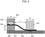
- Heating element 305 is provided in upper fixing jig 302, and an input temperature is measured by thermocouple 306 for measuring an input temperature at an interface between heating element 305 and bonded body sample 303.
- temperature control of the heating element was performed such that the input temperature of the thermocouple 306 for measuring an input temperature was set to be 55°C.
- the temperature of bonded body sample 303, which was increased by transfer of heat from heating element 305 was measured by thermocouple 307 for measuring a transfer temperature, and the measured temperature was used as a transfer temperature.
- Heat conductivity was evaluated by calculating a difference between the transfer temperature and the input temperature.
- a test was performed while holding jig 304 was cooled at a flow rate of 1 liter/min by using water of 25°C.
- An object having a width of 10 mm, a depth of 10 mm, and a height of 2 mm was used as fixing jig 302.
- An object having a width of 10 mm, a depth of 10 mm, and a height of 15 mm was used as holding jig 304.
- a distance L between an end portion of fixing jig 302 and an end portion of holding jig 304 was 15 mm.
- An object having a width of 5 mm, a depth of 5 mm, and a height of 3 mm was used as heating element 305. Heating element 305 was installed at the center of upper fixing jig 302 on the lower surface.
- Thermocouple 306 for measuring an input temperature was installed on the surface at the center of heating element 305 on the lower surface.
- Thermocouple 307 for measuring a transfer temperature was installed so as to interpose bonded body sample 303 between the center of holding jig 304 on the lower surface and thermocouple 307 for measuring a transfer temperature.
- Table 1 shows the thickness of the compound layer in each of Examples 1 to 12 and Comparative Examples 1 to 4, the composition ratio of the compound layer, and test results and evaluation results of heat conductivity and flexibility, which were obtained by the above test and the above observation.
- the heat conductivity was determined based on a decrease rate of the heat conductivity.
- the highly-aligned graphite in Comparative Example 1 has the same thickness as the sum of the thickness of first member 101 and second member 102 in Example 1.
- a case where the decrease rate was equal to or smaller than 10% was set to be "A”.
- a case where the decrease rate was greater than 10% and smaller than 16% was set to be “B”.
- a case where the decrease rate was equal to or greater than 16% was set to be "C”.
- the determination is "A”
- the bonded body has sufficient heat dissipation properties and does not cause degradation of performance of a CPU even when being used as a heat dissipation member, in a product.
- the determination is "B”
- degradation of performance of a CPU does not occur, but the temperature is increased.
- a CPU is not operated because it is not possible to dissipate generated heat.
- Example 1 Thickness (mm) of bonded member First element Content (wt%) of first element Thickness ( ⁇ m) of compound layer Composition ratio of compound layer First element/tin/carbon (wt%/wt%/wt%) Temperature difference (°C) Decrease rate (%) Heat conductivity Flexibility
- Example 1 0.1 Titanium 0.1 0.4 55/10/35 12.7 5.8 A ⁇
- Example 2 0.1 Titanium 2 6 68/5/27 13 8.3 A ⁇
- Example 3 0.1 Titanium 5 10 80/1/19 13.5 12.5 B ⁇
- Example 4 0.5 Titanium 0.1 0.1 50/15/35 3.2 6.7 A ⁇
- Example 5 0.5 Titanium 1 3 64/7/29 3.3 10 A ⁇
- Example 6 0.5 Titanium 5 9 80/5/15/15 3.4 13.3 B ⁇
- Example 7 0.1 Zirconium 0.1 0.3 53/13/34 12.9 7.5
- Example 8 0.5 Vanadium 5 10 80/3/17 3.4 13.3 B ⁇
- Example 9 0.1 Titanium
- the thickness of the bonded member was 0.1 mm, and the titanium content of the bonding material was at least 0.1 wt% to at most 5 wt%.
- the temperature difference of such a bonded body was 12.7°C to 13.5°C and the decrease rate was 5.8% to 12.5%. This was a result which was substantially equivalent to the temperature difference of 12°C in Comparative Example 1 in which the bonding material was not used and only a carbon material was used. Thus, favorable heat transferability was obtained. Even in a case of the result obtained by observing the section, cracks were not viewed in the bonding material layer or the compound layer.
- the thickness of the bonded member was 0.5 mm, and the titanium content of the bonding material was at least 0.1 wt% to at most 5 wt%.
- the temperature difference of such a bonded body was 3.2°C to 3.4°C and the decrease rate was 6.7% to 13.3%. This was a result which was substantially equivalent to the temperature difference of 3°C in Comparative Example 2 in which the bonding material was not used and only a carbon material was used. Thus, favorable heat transferability was obtained. Even in a case of the result obtained by observing the section, cracks were not viewed in the bonding material layer or the compound layer.
- the thickness of the bonded member was 0.1 mm, and the titanium content of the bonding material was 0.05 wt% in Comparative Example 3 and 5.5 wt% in Comparative Example 4.
- the temperature difference of the bonded body was 17°C in Comparative Example 3 and 16°C in Comparative Example 4.
- the decrease rate was 41.7% in Comparative Example 3 and 33.3% in Comparative Example 4.
- the bonding material had multiple voids without being wet by the carbon material.
- it is considered that the heat conductivity in Comparative Example 3 is largely decreased in comparison to that in Comparative Example 1.
- Comparative Example 4 as the result obtained by observing the section, cracks were not viewed.
- compound layer 105 is formed to exceed 11 ⁇ m.
- the thickness of the bonding material layer including much Sn is small, flexibility of the junction is lost, and cracks occur. It is considered that the heat conductivity is largely reduced because cracks occur.
- Example 7 In the bonded body in Example 7, 0.1 wt% of zirconium as the compound-formable element was used, and the thickness of the bonded member was 0.1 mm. The temperature difference of such a bonded body was 12.9°C and the decrease rate was 7.5%. This was a result which was substantially equivalent to the temperature difference of 12°C in Comparative Example 1 in which the bonding material was not used and only a carbon material was used. Thus, favorable heat transferability was obtained. Cracks were not viewed in the bonding material or a bonding layer even from the result obtained by observing the section.
- Example 8 In the bonded body in Example 8, 5 wt% of vanadium as the compound-formable element was used, and the thickness of the bonded member was 0.5 mm. The temperature difference of such a bonded body was 3.4°C and the decrease rate was 13.3%. This was a result which was substantially equivalent to the temperature difference of 3°C in Comparative Example 2 in which the bonding material was not used and only a carbon material was used. Thus, favorable heat transferability was obtained. Cracks were not viewed in the bonding material or a bonding layer even from the result obtained by observing the section.
- the junction provided by the bonding material in the disclosure is firm, has heat dissipation properties, and has flexibility. Thus, it is possible to be also used in a heat generated portion in a semiconductor, industrial equipment, and the like.
Landscapes
- Engineering & Computer Science (AREA)
- Chemical & Material Sciences (AREA)
- Mechanical Engineering (AREA)
- Ceramic Engineering (AREA)
- Materials Engineering (AREA)
- Metallurgy (AREA)
- Organic Chemistry (AREA)
- Ceramic Products (AREA)
- Laminated Bodies (AREA)
Claims (3)
- Verfahren zur Herstellung eines Verbundkörpers (104), wobei das Verfahren umfasst:einen Schritt des Herstellens eines ersten Elements (101), eines zweiten Elements (102) und eines filmförmigen Bindungsmaterials (103),wobei jedes von dem ersten Element (101) und dem zweiten Element (102) ein Kohlenstoffmaterial ist und wobei das filmförmige Bindungsmaterial (103) mindestens 0,1 Gew.-% bis höchstens 5 Gew.-% von mindestens einem Element umfasst, das gemeinsam mit Zinn und Kohlenstoff eine Verbindung bilden kann,wobei Elemente, die gemeinsam mit Zinn und Kohlenstoff eine Verbindung bilden können, ausgewählt werden aus der Gruppe, die besteht aus Ti, V und Zr, undwobei die Gesamtmenge von Elementen, die gemeinsam mit Zinn und Kohlenstoff eine Verbindung bilden können, mindestens 0,1 Gew.-% bis höchstens 5 Gew.-% beträgt, bezogen auf das Gesamtgewicht des filmförmigen Bindungsmaterials (103); und Sn als einzigen Rests;einen Schritt des Verbindens des ersten Elements (101) und des zweiten Elements (102) miteinander, wobei der Verbindungsschritt umfasst:Anordnen des filmförmigen Bindungsmaterials (103) zwischen dem ersten Element (101) und dem zweiten Element (102) ;Heißpressen auf dem ersten Element (101), dem zweiten Element (102) und dem Bindungsmaterial (103) unter einer Stickstoffatmosphäre bei 250 °C oder höher und 1500 °C oder niedriger während einer geeigneten Zeit;und dann Kühlen;dadurch Bilden eines Übergangs (107), der durch eine Bindungsmaterialschicht (106) und eine Verbindungsschicht (105) ausgestaltet ist,wobei die Verbindungsschicht (105) aus einer Verbindung des mindestens einen Elements, Zinn und Kohlenstoff an einer Grenzfläche zwischen dem ersten Element (101) und der Bindungsmaterialschicht (106) und einer Grenzfläche zwischen dem zweiten Element (102) und der Bindungsmaterialschicht (106) ausgestaltet ist.
- Verbundkörper (104), der durch das Verfahren nach Anspruch 1 erhältlich ist, umfassend:ein erstes Element (101);ein zweites Element (102); undeinen Übergang (107), der zwischen dem ersten Element (101) und dem zweiten Element (102) bereitgestellt ist,wobei jedes von dem ersten Element (101) und dem zweiten Element (102) ein Kohlenstoffmaterial ist,wobei der Übergang (107) umfasst:eine Bindungsmaterialschicht (106),eine erste Verbindungsschicht (105), die an einer Grenzfläche zwischen dem ersten Element (101) und der Bindungsmaterialschicht (106) gebildet ist,eine zweite Verbindungsschicht (105), die an einer Grenzfläche zwischen dem zweiten Element (102) und der Bindungsmaterialschicht (106) gebildet ist,wobei der Übergang (107) mindestens eines von Titan, Zirconium und Vanadium als ein verbindungsbildbares Element und Sn als eine Hauptkomponente enthält, undwobei die erste und die zweite Verbindungsschicht (105) eine Konzentration des verbindungsbildbaren Elements aufweisen, die höher als die Konzentration des verbindungsbildbaren Elements in der Bindungsmaterialschicht (106) ist.
- Verbundkörper nach Anspruch 2,
wobei jede von der ersten und der zweiten Verbindungschicht (105) eine Dicke von einschließlich 0,1 µm bis 10 µm aufweist.
Applications Claiming Priority (1)
| Application Number | Priority Date | Filing Date | Title |
|---|---|---|---|
| JP2016237027A JP6799790B2 (ja) | 2016-12-06 | 2016-12-06 | 接合材とそれにより得られる接合体と接合体の製造方法 |
Publications (2)
| Publication Number | Publication Date |
|---|---|
| EP3335828A1 EP3335828A1 (de) | 2018-06-20 |
| EP3335828B1 true EP3335828B1 (de) | 2025-01-01 |
Family
ID=60569558
Family Applications (1)
| Application Number | Title | Priority Date | Filing Date |
|---|---|---|---|
| EP17201231.2A Active EP3335828B1 (de) | 2016-12-06 | 2017-11-13 | Verfahren zur herstellung eines verbundkörpers und nach diesem verfahren hergestellter verbundkörper |
Country Status (4)
| Country | Link |
|---|---|
| US (1) | US20180154612A1 (de) |
| EP (1) | EP3335828B1 (de) |
| JP (1) | JP6799790B2 (de) |
| CN (1) | CN108155161B (de) |
Families Citing this family (3)
| Publication number | Priority date | Publication date | Assignee | Title |
|---|---|---|---|---|
| JP2018093119A (ja) * | 2016-12-06 | 2018-06-14 | パナソニックIpマネジメント株式会社 | ヒートシンク |
| US11476399B2 (en) | 2017-11-29 | 2022-10-18 | Panasonic Intellectual Property Management Co., Ltd. | Jointing material, fabrication method for semiconductor device using the jointing material, and semiconductor device |
| CN113508462B (zh) * | 2019-09-02 | 2024-09-20 | 株式会社东芝 | 接合体、电路基板及半导体装置 |
Citations (2)
| Publication number | Priority date | Publication date | Assignee | Title |
|---|---|---|---|---|
| US4797328A (en) * | 1986-02-19 | 1989-01-10 | Degussa Aktiengesellschaft | Soft-solder alloy for bonding ceramic articles |
| JPH0195893A (ja) * | 1987-10-08 | 1989-04-13 | Seiko Instr & Electron Ltd | ろう材 |
Family Cites Families (12)
| Publication number | Priority date | Publication date | Assignee | Title |
|---|---|---|---|---|
| US3484210A (en) * | 1964-10-19 | 1969-12-16 | Henry J Pinter | Alloy coated carbon and graphite members having conductors soldered thereto |
| US3361561A (en) * | 1964-10-19 | 1968-01-02 | George E Schick | Alloys for soldering conductors to carbon and graphite |
| JPS5930604B2 (ja) | 1974-10-24 | 1984-07-27 | 石川島播磨重工業株式会社 | 都市ごみ空気輸送システムにおける圧力検出制御方法 |
| DE19526822C2 (de) * | 1995-07-15 | 1998-07-02 | Euromat Gmbh | Lotlegierung, Verwendung der Lotlegierung und Verfahren zum Verbinden von Werkstücken durch Löten |
| JP4151859B2 (ja) * | 1998-10-09 | 2008-09-17 | 第一高周波工業株式会社 | スパッタリング用ターゲット板の接合方法 |
| JP2000326088A (ja) * | 1999-03-16 | 2000-11-28 | Nippon Sheet Glass Co Ltd | 無鉛ハンダ |
| JP2001058287A (ja) * | 1999-06-11 | 2001-03-06 | Nippon Sheet Glass Co Ltd | 無鉛ハンダ |
| CA2340393A1 (en) * | 1999-06-11 | 2000-12-21 | Katsuaki Suganuma | Lead-free solder |
| US20140086670A1 (en) * | 2011-05-27 | 2014-03-27 | Toyo Tanso Co., Ltd. | Joint of metal material and ceramic-carbon composite material, method for producing same, carbon material joint, jointing material for carbon material joint, and method for producing carbon material joint |
| JP2012246172A (ja) | 2011-05-27 | 2012-12-13 | Toyo Tanso Kk | 金属材とセラミックス−炭素複合材との接合体及びその製造方法 |
| GB201312388D0 (en) * | 2013-07-10 | 2013-08-21 | Cambridge Entpr Ltd | Materials and methods for soldering and soldered products |
| US20150118514A1 (en) * | 2013-10-30 | 2015-04-30 | Teledyne Scientific & Imaging, Llc. | High Performance Thermal Interface System With Improved Heat Spreading and CTE Compliance |
-
2016
- 2016-12-06 JP JP2016237027A patent/JP6799790B2/ja active Active
-
2017
- 2017-11-13 EP EP17201231.2A patent/EP3335828B1/de active Active
- 2017-11-20 US US15/817,344 patent/US20180154612A1/en not_active Abandoned
- 2017-12-04 CN CN201711258638.5A patent/CN108155161B/zh active Active
Patent Citations (2)
| Publication number | Priority date | Publication date | Assignee | Title |
|---|---|---|---|---|
| US4797328A (en) * | 1986-02-19 | 1989-01-10 | Degussa Aktiengesellschaft | Soft-solder alloy for bonding ceramic articles |
| JPH0195893A (ja) * | 1987-10-08 | 1989-04-13 | Seiko Instr & Electron Ltd | ろう材 |
Also Published As
| Publication number | Publication date |
|---|---|
| JP2018090460A (ja) | 2018-06-14 |
| JP6799790B2 (ja) | 2020-12-16 |
| CN108155161A (zh) | 2018-06-12 |
| CN108155161B (zh) | 2023-03-28 |
| US20180154612A1 (en) | 2018-06-07 |
| EP3335828A1 (de) | 2018-06-20 |
Similar Documents
| Publication | Publication Date | Title |
|---|---|---|
| US10485112B2 (en) | Ceramic circuit substrate and method for producing ceramic circuit substrate | |
| US9188397B2 (en) | Dense composite material, method for producing the same, and component for semiconductor production equipment | |
| US11570890B2 (en) | Ceramic circuit board and module using same | |
| EP3335828B1 (de) | Verfahren zur herstellung eines verbundkörpers und nach diesem verfahren hergestellter verbundkörper | |
| CN109690760B (zh) | 散热板及其制造方法 | |
| KR102326618B1 (ko) | 구리판 부착 절연 기판용 구리판재 및 그 제조 방법 | |
| JP7273374B2 (ja) | 複合材料、及び複合材料の製造方法 | |
| EP3712935A1 (de) | Wärmeableitplatte und verfahren zu ihrer herstellung | |
| EP3553817A1 (de) | Verbundelement, wärmeableitungselement, halbleiterbauelement und verfahren zur herstellung eines verbundelements | |
| JP7196193B2 (ja) | 放熱部材 | |
| EP3109222A1 (de) | Keramikleiterplatte | |
| WO2020209121A1 (ja) | 接合基板及び接合基板の製造方法 | |
| WO2019189329A1 (ja) | ヒートシンク付き絶縁回路基板 | |
| EP3104406B1 (de) | Leistungsmodul | |
| JP2018162518A (ja) | ベーパーチャンバー用銅合金板及びベーパーチャンバー | |
| EP3872204A1 (de) | Verbundelement | |
| JP6590322B2 (ja) | グラファイトとシリコンとの結合体及びその製造方法 | |
| JP6066644B2 (ja) | セラミックス接合体の製造方法 | |
| JP2007142126A (ja) | 複合材料及び半導体搭載用放熱基板、及びそれを用いたセラミックパッケージ | |
| CN111682002A (zh) | 散热板 | |
| KR20230164796A (ko) | 복합재료 및 이 복합재료를 포함하는 방열부품 | |
| JP4244210B2 (ja) | アルミニウム−セラミックス複合体及びその製造方法 | |
| Leveugle et al. | Free standing thermal interface material based on vertical arrays composites | |
| US20230260868A1 (en) | Bonded body, ceramic-copper circuit board, and semiconductor device | |
| EP4043203B1 (de) | Verbundsubstrat und verfahren zu seiner herstellung und schaltungssubstrat und verfahren zu seiner herstellung |
Legal Events
| Date | Code | Title | Description |
|---|---|---|---|
| PUAI | Public reference made under article 153(3) epc to a published international application that has entered the european phase |
Free format text: ORIGINAL CODE: 0009012 |
|
| STAA | Information on the status of an ep patent application or granted ep patent |
Free format text: STATUS: THE APPLICATION HAS BEEN PUBLISHED |
|
| AK | Designated contracting states |
Kind code of ref document: A1 Designated state(s): AL AT BE BG CH CY CZ DE DK EE ES FI FR GB GR HR HU IE IS IT LI LT LU LV MC MK MT NL NO PL PT RO RS SE SI SK SM TR |
|
| AX | Request for extension of the european patent |
Extension state: BA ME |
|
| STAA | Information on the status of an ep patent application or granted ep patent |
Free format text: STATUS: REQUEST FOR EXAMINATION WAS MADE |
|
| 17P | Request for examination filed |
Effective date: 20181102 |
|
| RBV | Designated contracting states (corrected) |
Designated state(s): AL AT BE BG CH CY CZ DE DK EE ES FI FR GB GR HR HU IE IS IT LI LT LU LV MC MK MT NL NO PL PT RO RS SE SI SK SM TR |
|
| STAA | Information on the status of an ep patent application or granted ep patent |
Free format text: STATUS: EXAMINATION IS IN PROGRESS |
|
| 17Q | First examination report despatched |
Effective date: 20190206 |
|
| GRAP | Despatch of communication of intention to grant a patent |
Free format text: ORIGINAL CODE: EPIDOSNIGR1 |
|
| STAA | Information on the status of an ep patent application or granted ep patent |
Free format text: STATUS: GRANT OF PATENT IS INTENDED |
|
| INTG | Intention to grant announced |
Effective date: 20240611 |
|
| RIC1 | Information provided on ipc code assigned before grant |
Ipc: H01L 21/48 20060101ALN20240531BHEP Ipc: H01L 23/373 20060101ALN20240531BHEP Ipc: B32B 15/20 20060101ALI20240531BHEP Ipc: B32B 15/04 20060101ALI20240531BHEP Ipc: B32B 9/04 20060101ALI20240531BHEP Ipc: B32B 7/12 20060101ALI20240531BHEP Ipc: B32B 7/10 20060101ALI20240531BHEP Ipc: B32B 1/00 20060101ALI20240531BHEP Ipc: B32B 9/00 20060101ALI20240531BHEP Ipc: B23K 103/08 20060101ALI20240531BHEP Ipc: C22C 13/00 20060101ALI20240531BHEP Ipc: B23K 35/26 20060101AFI20240531BHEP |
|
| GRAS | Grant fee paid |
Free format text: ORIGINAL CODE: EPIDOSNIGR3 |
|
| GRAA | (expected) grant |
Free format text: ORIGINAL CODE: 0009210 |
|
| STAA | Information on the status of an ep patent application or granted ep patent |
Free format text: STATUS: THE PATENT HAS BEEN GRANTED |
|
| AK | Designated contracting states |
Kind code of ref document: B1 Designated state(s): AL AT BE BG CH CY CZ DE DK EE ES FI FR GB GR HR HU IE IS IT LI LT LU LV MC MK MT NL NO PL PT RO RS SE SI SK SM TR |
|
| REG | Reference to a national code |
Ref country code: GB Ref legal event code: FG4D |
|
| REG | Reference to a national code |
Ref country code: DE Ref legal event code: R096 Ref document number: 602017087055 Country of ref document: DE |
|
| REG | Reference to a national code |
Ref country code: CH Ref legal event code: EP |
|
| REG | Reference to a national code |
Ref country code: IE Ref legal event code: FG4D |
|
| REG | Reference to a national code |
Ref country code: LT Ref legal event code: MG9D |
|
| REG | Reference to a national code |
Ref country code: NL Ref legal event code: MP Effective date: 20250101 |
|
| REG | Reference to a national code |
Ref country code: AT Ref legal event code: MK05 Ref document number: 1755735 Country of ref document: AT Kind code of ref document: T Effective date: 20250101 |
|
| PG25 | Lapsed in a contracting state [announced via postgrant information from national office to epo] |
Ref country code: NL Free format text: LAPSE BECAUSE OF FAILURE TO SUBMIT A TRANSLATION OF THE DESCRIPTION OR TO PAY THE FEE WITHIN THE PRESCRIBED TIME-LIMIT Effective date: 20250101 |
|
| PG25 | Lapsed in a contracting state [announced via postgrant information from national office to epo] |
Ref country code: FI Free format text: LAPSE BECAUSE OF FAILURE TO SUBMIT A TRANSLATION OF THE DESCRIPTION OR TO PAY THE FEE WITHIN THE PRESCRIBED TIME-LIMIT Effective date: 20250101 |
|
| PG25 | Lapsed in a contracting state [announced via postgrant information from national office to epo] |
Ref country code: PL Free format text: LAPSE BECAUSE OF FAILURE TO SUBMIT A TRANSLATION OF THE DESCRIPTION OR TO PAY THE FEE WITHIN THE PRESCRIBED TIME-LIMIT Effective date: 20250101 |
|
| PG25 | Lapsed in a contracting state [announced via postgrant information from national office to epo] |
Ref country code: ES Free format text: LAPSE BECAUSE OF FAILURE TO SUBMIT A TRANSLATION OF THE DESCRIPTION OR TO PAY THE FEE WITHIN THE PRESCRIBED TIME-LIMIT Effective date: 20250101 |
|
| PG25 | Lapsed in a contracting state [announced via postgrant information from national office to epo] |
Ref country code: NO Free format text: LAPSE BECAUSE OF FAILURE TO SUBMIT A TRANSLATION OF THE DESCRIPTION OR TO PAY THE FEE WITHIN THE PRESCRIBED TIME-LIMIT Effective date: 20250401 Ref country code: IS Free format text: LAPSE BECAUSE OF FAILURE TO SUBMIT A TRANSLATION OF THE DESCRIPTION OR TO PAY THE FEE WITHIN THE PRESCRIBED TIME-LIMIT Effective date: 20250501 |
|
| PG25 | Lapsed in a contracting state [announced via postgrant information from national office to epo] |
Ref country code: HR Free format text: LAPSE BECAUSE OF FAILURE TO SUBMIT A TRANSLATION OF THE DESCRIPTION OR TO PAY THE FEE WITHIN THE PRESCRIBED TIME-LIMIT Effective date: 20250101 |
|
| PG25 | Lapsed in a contracting state [announced via postgrant information from national office to epo] |
Ref country code: PT Free format text: LAPSE BECAUSE OF FAILURE TO SUBMIT A TRANSLATION OF THE DESCRIPTION OR TO PAY THE FEE WITHIN THE PRESCRIBED TIME-LIMIT Effective date: 20250502 Ref country code: LV Free format text: LAPSE BECAUSE OF FAILURE TO SUBMIT A TRANSLATION OF THE DESCRIPTION OR TO PAY THE FEE WITHIN THE PRESCRIBED TIME-LIMIT Effective date: 20250101 |
|
| PG25 | Lapsed in a contracting state [announced via postgrant information from national office to epo] |
Ref country code: BG Free format text: LAPSE BECAUSE OF FAILURE TO SUBMIT A TRANSLATION OF THE DESCRIPTION OR TO PAY THE FEE WITHIN THE PRESCRIBED TIME-LIMIT Effective date: 20250101 Ref country code: GR Free format text: LAPSE BECAUSE OF FAILURE TO SUBMIT A TRANSLATION OF THE DESCRIPTION OR TO PAY THE FEE WITHIN THE PRESCRIBED TIME-LIMIT Effective date: 20250402 |
|
| PG25 | Lapsed in a contracting state [announced via postgrant information from national office to epo] |
Ref country code: AT Free format text: LAPSE BECAUSE OF FAILURE TO SUBMIT A TRANSLATION OF THE DESCRIPTION OR TO PAY THE FEE WITHIN THE PRESCRIBED TIME-LIMIT Effective date: 20250101 |
|
| PG25 | Lapsed in a contracting state [announced via postgrant information from national office to epo] |
Ref country code: CZ Free format text: LAPSE BECAUSE OF FAILURE TO SUBMIT A TRANSLATION OF THE DESCRIPTION OR TO PAY THE FEE WITHIN THE PRESCRIBED TIME-LIMIT Effective date: 20250101 |
|
| PG25 | Lapsed in a contracting state [announced via postgrant information from national office to epo] |
Ref country code: SE Free format text: LAPSE BECAUSE OF FAILURE TO SUBMIT A TRANSLATION OF THE DESCRIPTION OR TO PAY THE FEE WITHIN THE PRESCRIBED TIME-LIMIT Effective date: 20250101 |
|
| REG | Reference to a national code |
Ref country code: DE Ref legal event code: R097 Ref document number: 602017087055 Country of ref document: DE |
|
| PG25 | Lapsed in a contracting state [announced via postgrant information from national office to epo] |
Ref country code: SM Free format text: LAPSE BECAUSE OF FAILURE TO SUBMIT A TRANSLATION OF THE DESCRIPTION OR TO PAY THE FEE WITHIN THE PRESCRIBED TIME-LIMIT Effective date: 20250101 |
|
| PG25 | Lapsed in a contracting state [announced via postgrant information from national office to epo] |
Ref country code: DK Free format text: LAPSE BECAUSE OF FAILURE TO SUBMIT A TRANSLATION OF THE DESCRIPTION OR TO PAY THE FEE WITHIN THE PRESCRIBED TIME-LIMIT Effective date: 20250101 |
|
| PG25 | Lapsed in a contracting state [announced via postgrant information from national office to epo] |
Ref country code: IT Free format text: LAPSE BECAUSE OF FAILURE TO SUBMIT A TRANSLATION OF THE DESCRIPTION OR TO PAY THE FEE WITHIN THE PRESCRIBED TIME-LIMIT Effective date: 20250101 |
|
| PG25 | Lapsed in a contracting state [announced via postgrant information from national office to epo] |
Ref country code: EE Free format text: LAPSE BECAUSE OF FAILURE TO SUBMIT A TRANSLATION OF THE DESCRIPTION OR TO PAY THE FEE WITHIN THE PRESCRIBED TIME-LIMIT Effective date: 20250101 |
|
| PG25 | Lapsed in a contracting state [announced via postgrant information from national office to epo] |
Ref country code: RO Free format text: LAPSE BECAUSE OF FAILURE TO SUBMIT A TRANSLATION OF THE DESCRIPTION OR TO PAY THE FEE WITHIN THE PRESCRIBED TIME-LIMIT Effective date: 20250101 |
|
| PG25 | Lapsed in a contracting state [announced via postgrant information from national office to epo] |
Ref country code: SK Free format text: LAPSE BECAUSE OF FAILURE TO SUBMIT A TRANSLATION OF THE DESCRIPTION OR TO PAY THE FEE WITHIN THE PRESCRIBED TIME-LIMIT Effective date: 20250101 |
|
| PLBE | No opposition filed within time limit |
Free format text: ORIGINAL CODE: 0009261 |
|
| STAA | Information on the status of an ep patent application or granted ep patent |
Free format text: STATUS: NO OPPOSITION FILED WITHIN TIME LIMIT |
|
| 26N | No opposition filed |
Effective date: 20251002 |
|
| PGFP | Annual fee paid to national office [announced via postgrant information from national office to epo] |
Ref country code: DE Payment date: 20251119 Year of fee payment: 9 |