EP3334566B1 - Wafer chuck featuring reduced friction support surface - Google Patents
Wafer chuck featuring reduced friction support surface Download PDFInfo
- Publication number
- EP3334566B1 EP3334566B1 EP16837531.9A EP16837531A EP3334566B1 EP 3334566 B1 EP3334566 B1 EP 3334566B1 EP 16837531 A EP16837531 A EP 16837531A EP 3334566 B1 EP3334566 B1 EP 3334566B1
- Authority
- EP
- European Patent Office
- Prior art keywords
- wafer
- wafer chuck
- scratches
- chuck
- friction
- Prior art date
- Legal status (The legal status is an assumption and is not a legal conclusion. Google has not performed a legal analysis and makes no representation as to the accuracy of the status listed.)
- Active
Links
- 235000012431 wafers Nutrition 0.000 description 68
- 238000000034 method Methods 0.000 description 14
- 230000003746 surface roughness Effects 0.000 description 14
- 239000004065 semiconductor Substances 0.000 description 6
- 238000001459 lithography Methods 0.000 description 5
- 239000000463 material Substances 0.000 description 5
- 238000004519 manufacturing process Methods 0.000 description 4
- HBMJWWWQQXIZIP-UHFFFAOYSA-N silicon carbide Chemical compound [Si+]#[C-] HBMJWWWQQXIZIP-UHFFFAOYSA-N 0.000 description 4
- 229910010271 silicon carbide Inorganic materials 0.000 description 4
- 238000013461 design Methods 0.000 description 3
- 238000005498 polishing Methods 0.000 description 3
- 239000000758 substrate Substances 0.000 description 3
- VYPSYNLAJGMNEJ-UHFFFAOYSA-N Silicium dioxide Chemical compound O=[Si]=O VYPSYNLAJGMNEJ-UHFFFAOYSA-N 0.000 description 2
- 238000012545 processing Methods 0.000 description 2
- XUIMIQQOPSSXEZ-UHFFFAOYSA-N Silicon Chemical compound [Si] XUIMIQQOPSSXEZ-UHFFFAOYSA-N 0.000 description 1
- 238000005299 abrasion Methods 0.000 description 1
- 239000000919 ceramic Substances 0.000 description 1
- 239000002131 composite material Substances 0.000 description 1
- 230000001010 compromised effect Effects 0.000 description 1
- 238000011109 contamination Methods 0.000 description 1
- 238000001816 cooling Methods 0.000 description 1
- 230000001419 dependent effect Effects 0.000 description 1
- 238000009826 distribution Methods 0.000 description 1
- 230000005670 electromagnetic radiation Effects 0.000 description 1
- PCHJSUWPFVWCPO-UHFFFAOYSA-N gold Chemical compound [Au] PCHJSUWPFVWCPO-UHFFFAOYSA-N 0.000 description 1
- 239000010931 gold Substances 0.000 description 1
- 229910052737 gold Inorganic materials 0.000 description 1
- 230000003116 impacting effect Effects 0.000 description 1
- 238000011065 in-situ storage Methods 0.000 description 1
- 238000007373 indentation Methods 0.000 description 1
- 229910044991 metal oxide Inorganic materials 0.000 description 1
- 150000004706 metal oxides Chemical class 0.000 description 1
- 238000012986 modification Methods 0.000 description 1
- 230000004048 modification Effects 0.000 description 1
- 230000003287 optical effect Effects 0.000 description 1
- 238000006748 scratching Methods 0.000 description 1
- 230000002393 scratching effect Effects 0.000 description 1
- 229910052710 silicon Inorganic materials 0.000 description 1
- 239000010703 silicon Substances 0.000 description 1
- 235000012239 silicon dioxide Nutrition 0.000 description 1
- 239000000377 silicon dioxide Substances 0.000 description 1
- 238000003860 storage Methods 0.000 description 1
- 238000012360 testing method Methods 0.000 description 1
- 238000012876 topography Methods 0.000 description 1
Images


Classifications
-
- H—ELECTRICITY
- H01—ELECTRIC ELEMENTS
- H01L—SEMICONDUCTOR DEVICES NOT COVERED BY CLASS H10
- H01L21/00—Processes or apparatus adapted for the manufacture or treatment of semiconductor or solid state devices or of parts thereof
- H01L21/67—Apparatus specially adapted for handling semiconductor or electric solid state devices during manufacture or treatment thereof; Apparatus specially adapted for handling wafers during manufacture or treatment of semiconductor or electric solid state devices or components ; Apparatus not specifically provided for elsewhere
- H01L21/683—Apparatus specially adapted for handling semiconductor or electric solid state devices during manufacture or treatment thereof; Apparatus specially adapted for handling wafers during manufacture or treatment of semiconductor or electric solid state devices or components ; Apparatus not specifically provided for elsewhere for supporting or gripping
- H01L21/687—Apparatus specially adapted for handling semiconductor or electric solid state devices during manufacture or treatment thereof; Apparatus specially adapted for handling wafers during manufacture or treatment of semiconductor or electric solid state devices or components ; Apparatus not specifically provided for elsewhere for supporting or gripping using mechanical means, e.g. chucks, clamps or pinches
- H01L21/68714—Apparatus specially adapted for handling semiconductor or electric solid state devices during manufacture or treatment thereof; Apparatus specially adapted for handling wafers during manufacture or treatment of semiconductor or electric solid state devices or components ; Apparatus not specifically provided for elsewhere for supporting or gripping using mechanical means, e.g. chucks, clamps or pinches the wafers being placed on a susceptor, stage or support
- H01L21/68735—Apparatus specially adapted for handling semiconductor or electric solid state devices during manufacture or treatment thereof; Apparatus specially adapted for handling wafers during manufacture or treatment of semiconductor or electric solid state devices or components ; Apparatus not specifically provided for elsewhere for supporting or gripping using mechanical means, e.g. chucks, clamps or pinches the wafers being placed on a susceptor, stage or support characterised by edge profile or support profile
-
- B—PERFORMING OPERATIONS; TRANSPORTING
- B24—GRINDING; POLISHING
- B24B—MACHINES, DEVICES, OR PROCESSES FOR GRINDING OR POLISHING; DRESSING OR CONDITIONING OF ABRADING SURFACES; FEEDING OF GRINDING, POLISHING, OR LAPPING AGENTS
- B24B37/00—Lapping machines or devices; Accessories
- B24B37/11—Lapping tools
- B24B37/12—Lapping plates for working plane surfaces
- B24B37/14—Lapping plates for working plane surfaces characterised by the composition or properties of the plate materials
-
- B—PERFORMING OPERATIONS; TRANSPORTING
- B24—GRINDING; POLISHING
- B24B—MACHINES, DEVICES, OR PROCESSES FOR GRINDING OR POLISHING; DRESSING OR CONDITIONING OF ABRADING SURFACES; FEEDING OF GRINDING, POLISHING, OR LAPPING AGENTS
- B24B37/00—Lapping machines or devices; Accessories
- B24B37/11—Lapping tools
- B24B37/12—Lapping plates for working plane surfaces
- B24B37/16—Lapping plates for working plane surfaces characterised by the shape of the lapping plate surface, e.g. grooved
-
- B—PERFORMING OPERATIONS; TRANSPORTING
- B24—GRINDING; POLISHING
- B24B—MACHINES, DEVICES, OR PROCESSES FOR GRINDING OR POLISHING; DRESSING OR CONDITIONING OF ABRADING SURFACES; FEEDING OF GRINDING, POLISHING, OR LAPPING AGENTS
- B24B37/00—Lapping machines or devices; Accessories
- B24B37/27—Work carriers
- B24B37/30—Work carriers for single side lapping of plane surfaces
-
- G—PHYSICS
- G03—PHOTOGRAPHY; CINEMATOGRAPHY; ANALOGOUS TECHNIQUES USING WAVES OTHER THAN OPTICAL WAVES; ELECTROGRAPHY; HOLOGRAPHY
- G03F—PHOTOMECHANICAL PRODUCTION OF TEXTURED OR PATTERNED SURFACES, e.g. FOR PRINTING, FOR PROCESSING OF SEMICONDUCTOR DEVICES; MATERIALS THEREFOR; ORIGINALS THEREFOR; APPARATUS SPECIALLY ADAPTED THEREFOR
- G03F7/00—Photomechanical, e.g. photolithographic, production of textured or patterned surfaces, e.g. printing surfaces; Materials therefor, e.g. comprising photoresists; Apparatus specially adapted therefor
- G03F7/70—Microphotolithographic exposure; Apparatus therefor
- G03F7/70691—Handling of masks or workpieces
- G03F7/707—Chucks, e.g. chucking or un-chucking operations or structural details
-
- H—ELECTRICITY
- H01—ELECTRIC ELEMENTS
- H01L—SEMICONDUCTOR DEVICES NOT COVERED BY CLASS H10
- H01L21/00—Processes or apparatus adapted for the manufacture or treatment of semiconductor or solid state devices or of parts thereof
- H01L21/67—Apparatus specially adapted for handling semiconductor or electric solid state devices during manufacture or treatment thereof; Apparatus specially adapted for handling wafers during manufacture or treatment of semiconductor or electric solid state devices or components ; Apparatus not specifically provided for elsewhere
- H01L21/683—Apparatus specially adapted for handling semiconductor or electric solid state devices during manufacture or treatment thereof; Apparatus specially adapted for handling wafers during manufacture or treatment of semiconductor or electric solid state devices or components ; Apparatus not specifically provided for elsewhere for supporting or gripping
- H01L21/687—Apparatus specially adapted for handling semiconductor or electric solid state devices during manufacture or treatment thereof; Apparatus specially adapted for handling wafers during manufacture or treatment of semiconductor or electric solid state devices or components ; Apparatus not specifically provided for elsewhere for supporting or gripping using mechanical means, e.g. chucks, clamps or pinches
- H01L21/68714—Apparatus specially adapted for handling semiconductor or electric solid state devices during manufacture or treatment thereof; Apparatus specially adapted for handling wafers during manufacture or treatment of semiconductor or electric solid state devices or components ; Apparatus not specifically provided for elsewhere for supporting or gripping using mechanical means, e.g. chucks, clamps or pinches the wafers being placed on a susceptor, stage or support
- H01L21/6875—Apparatus specially adapted for handling semiconductor or electric solid state devices during manufacture or treatment thereof; Apparatus specially adapted for handling wafers during manufacture or treatment of semiconductor or electric solid state devices or components ; Apparatus not specifically provided for elsewhere for supporting or gripping using mechanical means, e.g. chucks, clamps or pinches the wafers being placed on a susceptor, stage or support characterised by a plurality of individual support members, e.g. support posts or protrusions
-
- H—ELECTRICITY
- H01—ELECTRIC ELEMENTS
- H01L—SEMICONDUCTOR DEVICES NOT COVERED BY CLASS H10
- H01L21/00—Processes or apparatus adapted for the manufacture or treatment of semiconductor or solid state devices or of parts thereof
- H01L21/67—Apparatus specially adapted for handling semiconductor or electric solid state devices during manufacture or treatment thereof; Apparatus specially adapted for handling wafers during manufacture or treatment of semiconductor or electric solid state devices or components ; Apparatus not specifically provided for elsewhere
- H01L21/683—Apparatus specially adapted for handling semiconductor or electric solid state devices during manufacture or treatment thereof; Apparatus specially adapted for handling wafers during manufacture or treatment of semiconductor or electric solid state devices or components ; Apparatus not specifically provided for elsewhere for supporting or gripping
- H01L21/687—Apparatus specially adapted for handling semiconductor or electric solid state devices during manufacture or treatment thereof; Apparatus specially adapted for handling wafers during manufacture or treatment of semiconductor or electric solid state devices or components ; Apparatus not specifically provided for elsewhere for supporting or gripping using mechanical means, e.g. chucks, clamps or pinches
- H01L21/68714—Apparatus specially adapted for handling semiconductor or electric solid state devices during manufacture or treatment thereof; Apparatus specially adapted for handling wafers during manufacture or treatment of semiconductor or electric solid state devices or components ; Apparatus not specifically provided for elsewhere for supporting or gripping using mechanical means, e.g. chucks, clamps or pinches the wafers being placed on a susceptor, stage or support
- H01L21/68757—Apparatus specially adapted for handling semiconductor or electric solid state devices during manufacture or treatment thereof; Apparatus specially adapted for handling wafers during manufacture or treatment of semiconductor or electric solid state devices or components ; Apparatus not specifically provided for elsewhere for supporting or gripping using mechanical means, e.g. chucks, clamps or pinches the wafers being placed on a susceptor, stage or support characterised by a coating or a hardness or a material
-
- B—PERFORMING OPERATIONS; TRANSPORTING
- B23—MACHINE TOOLS; METAL-WORKING NOT OTHERWISE PROVIDED FOR
- B23B—TURNING; BORING
- B23B31/00—Chucks; Expansion mandrels; Adaptations thereof for remote control
- B23B31/02—Chucks
- B23B31/24—Chucks characterised by features relating primarily to remote control of the gripping means
- B23B31/28—Chucks characterised by features relating primarily to remote control of the gripping means using electric or magnetic means in the chuck
-
- B—PERFORMING OPERATIONS; TRANSPORTING
- B23—MACHINE TOOLS; METAL-WORKING NOT OTHERWISE PROVIDED FOR
- B23B—TURNING; BORING
- B23B31/00—Chucks; Expansion mandrels; Adaptations thereof for remote control
- B23B31/02—Chucks
- B23B31/24—Chucks characterised by features relating primarily to remote control of the gripping means
- B23B31/30—Chucks characterised by features relating primarily to remote control of the gripping means using fluid-pressure means in the chuck
- B23B31/307—Vacuum chucks
Definitions
- the present disclosure relates to a method for processing a chuck that handles semiconductor wafers, and a chuck prepared or resulting from such a method.
- the processed chuck features reduced friction between itself and the wafer, permitting the wafer to settle to a "flat" condition.
- the silicon wafers upon which are to be manufactured the microprocessor chips must be precisely placed in the processing machines.
- the wafers typically are handled by vacuum handling equipment.
- the wafers droop, ever-so-slightly under their own weight.
- the drooping wafer "wants" to flatten out, but may be hindered from doing so by friction between the wafer and chuck. This is sometimes referred to as a "stickiness" problem.
- Metal oxides are notable in this regard, and silicon dioxide is no exception.
- This particular engineering solution may take the form of designing a plurality of "plateaus" of uniform height, typically regularly spaced, into the wafer. These plateaus exist in many geometries, and go by many names including pins, burls, mesas, bumps, proud lands, proud rings, etc.
- the pins help in reducing the friction so that the wafer can move laterally across the pins as it flattens out upon settling on the pins.
- the pins help to reduce wafer sticking, but further improvements in this regard are needed.
- wafers lie flat against the support surface(s) of the chuck. Otherwise, the circuit pattern images that are projected onto the wafer may be out-of-focus. Furthermore, wafer lithography may involve multiple exposures, with re-location of the wafer between exposures. Thus, it is critical that there be a way to precisely re-align the wafer on the chuck relative to its first positioning so that the subsequent exposures will take place in the correct position on the wafer.
- NL 1 031 985 C2 discloses a method for manufacturing a device for supporting a substrate during the manufacture of semiconductor components, which device comprises a substantially flat plate having an upper surface, on which the substrate is to be positioned, the upper surface of which plate initially has a flat surface, whilst at least that part of said upper surface on which the substrate is to be positioned has a surface roughness.
- the surface roughness is formed contactless by pulsed electromagnetic radiation in the initial flat surface of the upper surface of the flat plate.
- the surface roughness is more in the form of a specific texture.
- the consists of a pattern of evenly distributed indentations, which are separated from each other by an upright material edge. It is also possible to realize a different texture form in the upper surface.
- ridges may function as supporting edges, for example, whilst the grooves present therebetween may function to pass a process gas therethrough, for example for cooling purposes.
- wafer chucks are never perfectly flat and often have a slight curvature in a random manner, such as orientations that are upwards (bowl) or downwards (dome) in shape.
- Figure 1 shows the various possibilities between the wafer and chuck for orientations that are flat, curved up, or curved down.
- wafers When wafers are located on the wafer chuck that have picked up a curvature due to normal process, they are required to return to the original clamping location by settling to flat. As discussed earlier, the wafer is required to relax in a manner that is predominately radial.
- the friction between two opposing and contacting surfaces depends not only on the roughness of the surfaces, but also on the contour or "shape" or topography of the roughness. For example, if the roughness has a directionality, the friction likely will also possess a directionality.
- the top or (a) plot is a profilometer trace of surface roughness for aligned grooves (a "ruling").
- the second (b) plot shows the slope of the surface roughness of the first plot.
- the third (c) plot is a map of friction force. The second and third plots show that friction force is proportional to the slope of the roughness.
- the top graph shows that friction will be least where a contacting surface is moving front-to-back (along axis 21), will be greater when the contacting surface is moving right-to-left (along axis 23), and will be greatest when the contacting surface is moving left-to-right (along axis 25), due to the directionality and asymmetry of the roughness in the bottom surface.
- the current designs are limited in that as the surface area is reduced by making more and more scratches, under this condition the wafer chuck becomes more susceptible to wear due to the higher localized pressure and reduced bearing area. The rougher the surface, the greater the likelihood of increased wear.
- the instant disclosure addresses these issues, and provides a solution.
- Grinding, lapping and polishing basically work by making scratches in the body being ground, lapped or polished.
- the scratches typically are linear.
- the scratches gives rise to a directionality component of friction: the friction coefficient is less in the direction along the scratch than in a direction orthogonal, or across, the scratch.
- a typical pin's bearing surface is fabricated by methods such as grinding, lapping or polishing, which intentionally generate random scratches in the surface where the wafer is in contact. These scratches in the surface are aligned in a more or less random manner; therefore, there is no preferential direction with less friction.
- a typical lapped pin is shown below in Figure 3 . When the data are clipped to show just the bearing surface where the wafer contacts the wafer chuck, the randomness of the scratching is more evident as shown in Figure 4 . Figure Cartesian space and the slope in the X and Y orthogonal directions is plotted.
- the tool here used to accomplish lapping is termed a "treatment tool".
- the treatment tool may have about the same hardness as the chuck, or at least the chuck surface that supports a wafer.
- One way to accomplish this is to fabricate the treatment tool from the same, or similar material as used to fabricate the chuck or chuck support surface.
- a popular choice in such materials is a ceramic such as silicon carbide (SiC), which may be in the form of a SiC-containing composite material such as reaction bonded SiC (“RB-SiC").
- the treatment tool typically features a flat surface (or one that appears flat visually) that is intended to mechanically or physically contact the surface of the work piece, for example, a wafer chuck.
- the treatment tool may be shaped as a ring or annulus. The tool is moved over the chuck surface while in physical contact with it, thus removing material by abrasion.
- the treatment tool is 27 mm in diameter.
- the contact surface appears to be a flat disc, but in reality it has a slight toroidal shape so that when it is brought into contact with the flat surface, the area of contact is not that of a disc but instead is a circle or annulus. If the contacting surface of the treatment tool is shaped as an annulus or ring, it, too, may feature a slightly toroidal shape.
- a wafer surface is populated with dies, or regions where a microprocessor will be formed by lithography.
- the size of a die may range from about 3 millimeters to about 28 millimeters.
- the size, diameter, or "effective diameter" of the treatment tool may be scaled to correspond to the die size on the wafer that is to undergo lithography. Thus, where the die size is 28 mm long, a 28 mm diameter lapping tool would be appropriate.
- the lapping that was carried out according to the instant disclosure made use of a 28 millimeter toroidal-shaped SiC-containing treatment tool under a dead weight load of about 180 grams, and operated at an average velocity of about 3 meters per minute. Visually, the treatment tool appeared disc-shaped; however, the edge and center regions of the disc were elevated away from flat to give the treatment tool a slightly toroidal shape.
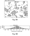
- Figure 5 features histograms showing the slope of the surface roughness in X ( Figures 5B ) and Y ( Figures 5D ) directions.
- the images ( Figures 5A and 5C ) above each histogram ( Figures 5B and 5D ) are photomicrographs of the surfaces where the surface roughness was measured.
- the RMS slope of surface roughness in the X-direction was 7.22 microns per millimeter.
- the RMS slope of surface roughness in the Y-direction, orthogonal to the X-direction was 7.24 microns per millimeter. Thus, the slopes are about the same, indicating a lack of directionality to the surface roughness.
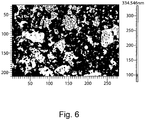
- the movement of the treatment tool was modified to see if the tool could impart a directionality to the surface roughness.
- the final strokes or passes of the treatment tool were made along a specific axis, namely, the Y-axis.
- the scratches imparted by the tool have a directionality, as seen in the photomicrograph that is Figure 6 .
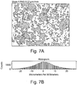
- Figures 7A-7D further document and quantify this directionality.
- Figures 7A and 7C are optical photomicrographs corresponding to the histograms of Figures 7B and 7D .
- the histograms report the distribution of slopes of the surface elevation.
- the slope in the Y-direction, along the direction of lapping was about the same as before, for the randomized lapping situation.
- the RMS slope in the X-direction, orthogonal to the Y-direction was much higher, at 9.26 microns per millimeter. Since frictional force is proportional to the slope of the elevation, the friction in the X-direction is expected to be greater than the friction in the Y-direction.
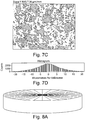
- a method to generate the features is by traveling across the wafer chuck through the center, as shown in Figure 8 . This may take compensation by changing the velocity and or the pressure to minimize the variation in the radial direction of the material that is removed.
- an alternate means to generate scratches that are very nearly radial is to have the final passes of the treatment tool describe a multi-pointed star pattern, with the next point of the star to be formed immediately after its adjacent star point.
- the treatment tool in its final passes takes a zig-zag path along the circumference of the wafer chuck, with the zigs and zags being toward and away from the center. In this way, the scratches formed by the treatment tool in its final passes will be close to radial directions.
- This design solves the stickiness problem by making small marks (e.g., scratches) on the bearing surface in a direction such that the surface is less restrictive and allows the wafer to relax.
- the preferred method to generate these scratches is a with a small tool lap, this lap can be more or less annular in shape to conformally "float" over the surface, thus minimally impacting gross curvature.
- One technique for accomplishing this behavior is to arrange that the treatment tool be minimally constrained in its attachment to its holder in the lapping machine, for example, by means of a ball-and-socket joint.
- the instant disclosure can be used in new wafer chucks that have not yet been placed in service. It can be used to repair wafer chucks that have already seen service. Furthermore, the repair of wafer chucks can take place in-situ; that is, without having to remove the wafer chuck from the lithography machine.
Description
- The present disclosure relates to a method for processing a chuck that handles semiconductor wafers, and a chuck prepared or resulting from such a method. The processed chuck features reduced friction between itself and the wafer, permitting the wafer to settle to a "flat" condition.
- As Moore's Law pushes semiconductor feature sizes smaller and smaller, the need for highly precise wafer handling components grows. The difficulty in achieving the required precision also grows. For instance, the silicon wafers upon which are to be manufactured the microprocessor chips must be precisely placed in the processing machines. The wafers typically are handled by vacuum handling equipment. The wafers droop, ever-so-slightly under their own weight. When lowered to a wafer chuck, the drooping wafer "wants" to flatten out, but may be hindered from doing so by friction between the wafer and chuck. This is sometimes referred to as a "stickiness" problem. Metal oxides are notable in this regard, and silicon dioxide is no exception. Among the efforts to solve, or at least ameliorate, this problem, have been to minimize the contact area between the wafer and the chuck. This particular engineering solution may take the form of designing a plurality of "plateaus" of uniform height, typically regularly spaced, into the wafer. These plateaus exist in many geometries, and go by many names including pins, burls, mesas, bumps, proud lands, proud rings, etc. The pins help in reducing the friction so that the wafer can move laterally across the pins as it flattens out upon settling on the pins. The pins help to reduce wafer sticking, but further improvements in this regard are needed.
- It is critical that wafers lie flat against the support surface(s) of the chuck. Otherwise, the circuit pattern images that are projected onto the wafer may be out-of-focus. Furthermore, wafer lithography may involve multiple exposures, with re-location of the wafer between exposures. Thus, it is critical that there be a way to precisely re-align the wafer on the chuck relative to its first positioning so that the subsequent exposures will take place in the correct position on the wafer.
-
NL 1 031 985 C2 - An invention is set out in the independent claim.
- Why are wafers not flat to begin with? When wafers are processed and by inherent limitations of the manufacture they are not flat. Often, processes performed in the front end semiconductor line add films to the wafer, which results in more or less curved wafers. This curvature can be any direction, upward or downwards. The majority of the departure from flat is in curvature and deformation is as a sphere and or cylindrical shape.
- Additionally, wafer chucks are never perfectly flat and often have a slight curvature in a random manner, such as orientations that are upwards (bowl) or downwards (dome) in shape.
Figure 1 shows the various possibilities between the wafer and chuck for orientations that are flat, curved up, or curved down. - When wafers are located on the wafer chuck that have picked up a curvature due to normal process, they are required to return to the original clamping location by settling to flat. As discussed earlier, the wafer is required to relax in a manner that is predominately radial.
- In semiconductor lithography, often there is a need for multiple exposures, but with the wafer being moved between exposures. When a shape mismatch occurs between the wafer and chuck, the wafer needs to slide and relax a very small amount to realign with a previously generated pattern. If the wafer chuck roughness is in such a manner that the wafer is unable to relax to the natural state (by sliding), then a second or subsequent pattern is misaligned; hence overlay becomes compromised.
- The friction between two opposing and contacting surfaces depends not only on the roughness of the surfaces, but also on the contour or "shape" or topography of the roughness. For example, if the roughness has a directionality, the friction likely will also possess a directionality.
- This is demonstrated below in
Figure 2 , with three graphs presented by Bharat Bhushan in his paper entitled, "Micro/Nanotribology and Micro-Nanomechanics of Magnetic Storage Devices", which is found between pages 1137 and 1197 in the reference book, Nanotribology and Nanomechanics, published by Springer Berlin Heidelberg in 2008. The top or (a) plot is a profilometer trace of surface roughness for aligned grooves (a "ruling"). The second (b) plot shows the slope of the surface roughness of the first plot. The third (c) plot is a map of friction force. The second and third plots show that friction force is proportional to the slope of the roughness. The top graph shows that friction will be least where a contacting surface is moving front-to-back (along axis 21), will be greater when the contacting surface is moving right-to-left (along axis 23), and will be greatest when the contacting surface is moving left-to-right (along axis 25), due to the directionality and asymmetry of the roughness in the bottom surface. - The current designs are limited in that as the surface area is reduced by making more and more scratches, under this condition the wafer chuck becomes more susceptible to wear due to the higher localized pressure and reduced bearing area. The rougher the surface, the greater the likelihood of increased wear.
- The instant disclosure addresses these issues, and provides a solution.
- Grinding, lapping and polishing basically work by making scratches in the body being ground, lapped or polished. The scratches typically are linear. The scratches gives rise to a directionality component of friction: the friction coefficient is less in the direction along the scratch than in a direction orthogonal, or across, the scratch.
- In a wafer handling/chucking situation, one wants the wafer to settle on the chuck, which involves the outer regions of the wafer moving radially with respect to the chuck. One can reduce friction in the radial direction by giving the lapping scratches a preferred orientation, namely, radial. This can be achieved by making the final passes of the lapping tool move predominantly in radial directions.
-
-
Figures 1A-1H shows various possibilities between the wafer and chuck for orientations that are flat, curved up, or curved down. -
Figure 2 : (a) surface roughness map, (b) slope of the roughness profile taken in the sample sliding direction (the horizontal axis), and (c) friction force map for a gold-coated ruling at a normal load of 155nN. -
Figure 3 : Typical pin surface showing residual scratches from the manufacturing process. -
Figure 4 : This shows the surface that is to be in contact with the wafer. -
Figure 5 showing slope plots indicating that the surface was more or less randomly scratched in the region where contact is made with the wafer. Specifically,Figures 5A and 5B are image and histogram corresponding to slope in the X direction, andFigures 5C and 5D are image and histogram corresponding to slope in the Y direction. -
Figure 6 shows a pin surface that has been final lapped along the Y-axis. -
Figure 7 shows the slope plot corresponding to the pin ofFigure 6 . Specifically,Figures 7A and 7B are image and histogram corresponding to slope in the X direction, andFigures 7C and 7D are image and histogram corresponding to slope in the Y direction. -
Figure 8 shows the generation of radial scratches to minimize the roughness along the settling direction of the wafer. Specifically,Figure 8A is a perspective view, andFigure 8B is a top or plan view of the radial scratches in a wafer chuck. - Grinding, lapping and polishing basically work by making scratches in the body being ground, lapped or polished. The scratches typically are linear. The scratches gives rise to a directionality component of friction: the friction coefficient is less in the direction along the scratch than in a direction orthogonal, or across, the scratch.
- Current techniques for lapping wafer chucks use a randomly generated roughness in a 'bearing' geometry (plateau) whereby the top contact region is minimized and the top surface roughness, commonly identified as "Spq", is maximized. This technique recognizes that the forces required to overcome the friction are proportional to the slope of the roughness. Steeper slopes generate more resistance to sliding.
- A typical pin's bearing surface is fabricated by methods such as grinding, lapping or polishing, which intentionally generate random scratches in the surface where the wafer is in contact. These scratches in the surface are aligned in a more or less random manner; therefore, there is no preferential direction with less friction. A typical lapped pin is shown below in
Figure 3 . When the data are clipped to show just the bearing surface where the wafer contacts the wafer chuck, the randomness of the scratching is more evident as shown inFigure 4 . Figure Cartesian space and the slope in the X and Y orthogonal directions is plotted. - The tool here used to accomplish lapping is termed a "treatment tool". In one embodiment, the treatment tool may have about the same hardness as the chuck, or at least the chuck surface that supports a wafer. One way to accomplish this is to fabricate the treatment tool from the same, or similar material as used to fabricate the chuck or chuck support surface. A popular choice in such materials is a ceramic such as silicon carbide (SiC), which may be in the form of a SiC-containing composite material such as reaction bonded SiC ("RB-SiC").
- The treatment tool typically features a flat surface (or one that appears flat visually) that is intended to mechanically or physically contact the surface of the work piece, for example, a wafer chuck. In another embodiment, the treatment tool may be shaped as a ring or annulus. The tool is moved over the chuck surface while in physical contact with it, thus removing material by abrasion.
- In one embodiment, the treatment tool is 27 mm in diameter. Visually, the contact surface appears to be a flat disc, but in reality it has a slight toroidal shape so that when it is brought into contact with the flat surface, the area of contact is not that of a disc but instead is a circle or annulus. If the contacting surface of the treatment tool is shaped as an annulus or ring, it, too, may feature a slightly toroidal shape.
- A wafer surface is populated with dies, or regions where a microprocessor will be formed by lithography. The size of a die may range from about 3 millimeters to about 28 millimeters. The size, diameter, or "effective diameter" of the treatment tool may be scaled to correspond to the die size on the wafer that is to undergo lithography. Thus, where the die size is 28 mm long, a 28 mm diameter lapping tool would be appropriate.
- The lapping that was carried out according to the instant disclosure made use of a 28 millimeter toroidal-shaped SiC-containing treatment tool under a dead weight load of about 180 grams, and operated at an average velocity of about 3 meters per minute. Visually, the treatment tool appeared disc-shaped; however, the edge and center regions of the disc were elevated away from flat to give the treatment tool a slightly toroidal shape.
-
Figure 5 features histograms showing the slope of the surface roughness in X (Figures 5B ) and Y (Figures 5D ) directions. The images (Figures 5A and5C ) above each histogram (Figures 5B and5D ) are photomicrographs of the surfaces where the surface roughness was measured. The RMS slope of surface roughness in the X-direction was 7.22 microns per millimeter. The RMS slope of surface roughness in the Y-direction, orthogonal to the X-direction, was 7.24 microns per millimeter. Thus, the slopes are about the same, indicating a lack of directionality to the surface roughness. - Next, the movement of the treatment tool was modified to see if the tool could impart a directionality to the surface roughness. Specifically, the final strokes or passes of the treatment tool were made along a specific axis, namely, the Y-axis. Certainly, the scratches imparted by the tool have a directionality, as seen in the photomicrograph that is
Figure 6 . -
Figures 7A-7D further document and quantify this directionality. Again,Figures 7A and7C are optical photomicrographs corresponding to the histograms ofFigures 7B and7D . The histograms report the distribution of slopes of the surface elevation. At an RMS of 7.26 microns per millimeter, the slope in the Y-direction, along the direction of lapping, was about the same as before, for the randomized lapping situation. Significantly, the RMS slope in the X-direction, orthogonal to the Y-direction, was much higher, at 9.26 microns per millimeter. Since frictional force is proportional to the slope of the elevation, the friction in the X-direction is expected to be greater than the friction in the Y-direction. - A method to generate the features is by traveling across the wafer chuck through the center, as shown in
Figure 8 . This may take compensation by changing the velocity and or the pressure to minimize the variation in the radial direction of the material that is removed. - If the treatment tool is constrained such that it cannot pass through the center of a wafer chuck, then an alternate means to generate scratches that are very nearly radial is to have the final passes of the treatment tool describe a multi-pointed star pattern, with the next point of the star to be formed immediately after its adjacent star point. In other words, the treatment tool in its final passes, takes a zig-zag path along the circumference of the wafer chuck, with the zigs and zags being toward and away from the center. In this way, the scratches formed by the treatment tool in its final passes will be close to radial directions.
- The results of the lapping tests corresponding to
Figures 5A through 7D indicate that a directionality can be imparted to the lapping process, that the slope of the surface elevation or surface roughness can be engineered and specifically, can be given a directionality. The results also suggest that the forces required to overcome friction between two surfaces can be given a directionality, and specifically suggest that the friction force orthogonal to the lapping direction will be greater than the friction force parallel to the lapping direction. Since wafers settling on a wafer chuck need to "relax" radially (that is, in radial directions), this suggests the lapping, or at least the final strokes of a lapping operation, should take place in radial directions along the wafer chuck support surface. - This design solves the stickiness problem by making small marks (e.g., scratches) on the bearing surface in a direction such that the surface is less restrictive and allows the wafer to relax.
- The preferred method to generate these scratches is a with a small tool lap, this lap can be more or less annular in shape to conformally "float" over the surface, thus minimally impacting gross curvature. One technique for accomplishing this behavior is to arrange that the treatment tool be minimally constrained in its attachment to its holder in the lapping machine, for example, by means of a ball-and-socket joint.
- When a surface is treated with a tool in a final lap along a specific axis, the roughness becomes larger in the slope of the opposing axis.
- What is proposed is a design whereby the slope of the interface surface between the wafer chuck and the wafer, along the direction of sliding is minimal (for a wafer chuck this is radial) yet the area remains constant, thus maintaining a nominal resistance to wear.
- The instant disclosure can be used in new wafer chucks that have not yet been placed in service. It can be used to repair wafer chucks that have already seen service. Furthermore, the repair of wafer chucks can take place in-situ; that is, without having to remove the wafer chuck from the lithography machine.
- Although much of the forgoing discussion has focused on articles and devices for chucking semiconductor wafers, one of ordinary skill in the art will recognize other related applications where the techniques and articles disclosed in the instant patent application will be useful, for example, in other fields and industries where one desires to engineer a low friction surface, or to engineer a surface whose friction is anisotropic, that is, direction-dependent.
- An artisan of ordinary skill will appreciate that various modifications may be made to the disclosure herein described without departing from the scope of the disclosure. The invention is defined by the appended claims.
Claims (9)
- A wafer chuck comprising a surface configured to support a wafer, said surface being processed tribologically such as to minimize the slope of the roughness of said surface as measured in a radial direction,wherein said surface comprises scratches oriented predominantly radially,wherein said surface has a lower coefficient of friction in a radial direction than in a circumferential direction.
- The wafer chuck of claim 1, wherein said surface comprises a center.
- The wafer chuck of claim 2, wherein said scratches pass through said center of said surface.
- The wafer chuck of claim 2, wherein said scratches do not pass through said center, and wherein said scratches form a zig-zag path along a circumference of said wafer chuck such that said scratches are close to radial directions.
- The wafer chuck of any preceding claim, wherein said surface comprises scratches in a star-shaped pattern, the star comprising at least eight points.
- The wafer chuck of any preceding claim, wherein said surface comprises a plurality of pins.
- The wafer chuck of any preceding claim, wherein said scratches are linear.
- The wafer chuck of any preceding claim, wherein said support surface comprises SiC.
- The wafer chuck of any preceding claim, wherein said surface comprises a plurality of pins, and said scratches are in a bearing surface of said pins.
Applications Claiming Priority (2)
| Application Number | Priority Date | Filing Date | Title |
|---|---|---|---|
| US201562205425P | 2015-08-14 | 2015-08-14 | |
| PCT/US2016/046436 WO2017030873A1 (en) | 2015-08-14 | 2016-08-10 | Wafer chuck featuring reduced friction support surface |
Publications (3)
| Publication Number | Publication Date |
|---|---|
| EP3334566A1 EP3334566A1 (en) | 2018-06-20 |
| EP3334566A4 EP3334566A4 (en) | 2019-06-19 |
| EP3334566B1 true EP3334566B1 (en) | 2021-11-24 |
Family
ID=58050865
Family Applications (1)
| Application Number | Title | Priority Date | Filing Date |
|---|---|---|---|
| EP16837531.9A Active EP3334566B1 (en) | 2015-08-14 | 2016-08-10 | Wafer chuck featuring reduced friction support surface |
Country Status (4)
| Country | Link |
|---|---|
| US (1) | US10790181B2 (en) |
| EP (1) | EP3334566B1 (en) |
| JP (1) | JP7041051B2 (en) |
| WO (1) | WO2017030873A1 (en) |
Families Citing this family (1)
| Publication number | Priority date | Publication date | Assignee | Title |
|---|---|---|---|---|
| US20210405539A1 (en) * | 2018-11-05 | 2021-12-30 | Asml Holding N.V. | A method to manufacture nano ridges in hard ceramic coatings |
Family Cites Families (51)
| Publication number | Priority date | Publication date | Assignee | Title |
|---|---|---|---|---|
| US4551192A (en) | 1983-06-30 | 1985-11-05 | International Business Machines Corporation | Electrostatic or vacuum pinchuck formed with microcircuit lithography |
| US4692836A (en) * | 1983-10-31 | 1987-09-08 | Toshiba Kikai Kabushiki Kaisha | Electrostatic chucks |
| US5342068A (en) * | 1993-08-26 | 1994-08-30 | Texas Instruments Incorporated | Laminar flow vacuum chuck |
| JPH07171747A (en) | 1993-12-21 | 1995-07-11 | Ricoh Co Ltd | Grinding and polishing device |
| US5692873A (en) | 1995-03-31 | 1997-12-02 | Motorola, Inc. | Apparatus for holding a piece of semiconductor |
| JPH0936070A (en) | 1995-07-21 | 1997-02-07 | Nippon Steel Corp | Polishing device of semiconductor wafer |
| JPH09191015A (en) * | 1996-01-11 | 1997-07-22 | Canon Inc | Heat treatment device |
| JPH1071562A (en) * | 1996-05-10 | 1998-03-17 | Canon Inc | Mechano-chemical polishing device and method |
| KR100264228B1 (en) | 1996-05-10 | 2000-12-01 | 미다라이 후지오 | Chemical mechanical polishing apparatus and method |
| US6217655B1 (en) | 1997-01-31 | 2001-04-17 | Applied Materials, Inc. | Stand-off pad for supporting a wafer on a substrate support chuck |
| US6063202A (en) * | 1997-09-26 | 2000-05-16 | Novellus Systems, Inc. | Apparatus for backside and edge exclusion of polymer film during chemical vapor deposition |
| JP2000061842A (en) | 1998-08-18 | 2000-02-29 | Toshiba Mach Co Ltd | Polishing device |
| US6215642B1 (en) | 1999-03-11 | 2001-04-10 | Nikon Corporation Of Japan | Vacuum compatible, deformable electrostatic chuck with high thermal conductivity |
| US6264467B1 (en) * | 1999-04-14 | 2001-07-24 | Applied Materials, Inc. | Micro grooved support surface for reducing substrate wear and slip formation |
| US6439986B1 (en) * | 1999-10-12 | 2002-08-27 | Hunatech Co., Ltd. | Conditioner for polishing pad and method for manufacturing the same |
| US6353271B1 (en) | 1999-10-29 | 2002-03-05 | Euv, Llc | Extreme-UV scanning wafer and reticle stages |
| EP1291910B1 (en) | 2000-01-28 | 2007-01-10 | Hitachi Tokyo Electronics Co., Ltd. | Wafer chuck, exposure system, and method of manufacturing semiconductor device |
| JP2002057209A (en) | 2000-06-01 | 2002-02-22 | Tokyo Electron Ltd | Single-wafer processing apparatus and single-wafer processing method |
| JP3859937B2 (en) | 2000-06-02 | 2006-12-20 | 住友大阪セメント株式会社 | Electrostatic chuck |
| US6717159B2 (en) | 2000-10-18 | 2004-04-06 | Nikon Corporation | Low distortion kinematic reticle support |
| KR100422444B1 (en) | 2001-05-29 | 2004-03-12 | 삼성전자주식회사 | wafer spacing support apparatus installed on electro static chuck and method for fabricating same |
| KR20120045040A (en) | 2002-12-20 | 2012-05-08 | 맷슨 테크날러지 캐나다 인코퍼레이티드 | Method for supporting a workpiece |
| KR100753302B1 (en) * | 2004-03-25 | 2007-08-29 | 이비덴 가부시키가이샤 | Vacuum chuck, suction board, polishing device, and method for manufacturing of semiconductor wafer |
| US7150677B2 (en) | 2004-09-22 | 2006-12-19 | Mitsubishi Materials Corporation | CMP conditioner |
| JP4049172B2 (en) | 2005-07-13 | 2008-02-20 | 住友電気工業株式会社 | Wafer holder for wafer prober and wafer prober equipped with the same |
| JP4756583B2 (en) | 2005-08-30 | 2011-08-24 | 株式会社東京精密 | Polishing pad, pad dressing evaluation method, and polishing apparatus |
| TWI327761B (en) * | 2005-10-07 | 2010-07-21 | Rohm & Haas Elect Mat | Method for making semiconductor wafer and wafer holding article |
| US8057633B2 (en) * | 2006-03-28 | 2011-11-15 | Tokyo Electron Limited | Post-etch treatment system for removing residue on a substrate |
| WO2007145505A1 (en) * | 2006-06-12 | 2007-12-21 | Xycarb Ceramics B.V. | Method for manufacturing a device for supporting a substrate during the manufacture of semiconductor components, as well as such a device |
| NL1031985C2 (en) * | 2006-06-12 | 2007-12-13 | Xycarb Ceramics B V | Method for manufacturing device for supporting substrate during semiconductor manufacture, involves forming surface roughness on upper surface of plate by electromagnetic radiation without disturbing initial flat surface of plate |
| US20080100812A1 (en) | 2006-10-26 | 2008-05-01 | Nikon Corporation | Immersion lithography system and method having a wafer chuck made of a porous material |
| JP5099476B2 (en) | 2006-12-28 | 2012-12-19 | 株式会社ニコン | Cleaning apparatus and cleaning system, pattern forming apparatus, cleaning method and exposure method, and device manufacturing method |
| JP4864757B2 (en) | 2007-02-14 | 2012-02-01 | 東京エレクトロン株式会社 | Substrate mounting table and surface treatment method thereof |
| JP5018249B2 (en) | 2007-06-04 | 2012-09-05 | 株式会社ニコン | Cleaning device, cleaning method, exposure apparatus, and device manufacturing method |
| JP5428171B2 (en) | 2008-03-12 | 2014-02-26 | 東ソー株式会社 | Polishing method |
| JP2010153407A (en) | 2008-12-23 | 2010-07-08 | Nikon Corp | Cleaning method and device, and exposure method and device |
| JP5402391B2 (en) * | 2009-01-27 | 2014-01-29 | 信越化学工業株式会社 | Method for processing synthetic quartz glass substrate for semiconductor |
| NL2004153A (en) | 2009-02-24 | 2010-08-25 | Asml Netherlands Bv | Lithographic apparatus, a method for removing material of one or more protrusions on a support surface, and an article support system. |
| US20100330890A1 (en) | 2009-06-30 | 2010-12-30 | Zine-Eddine Boutaghou | Polishing pad with array of fluidized gimballed abrasive members |
| JP5810517B2 (en) | 2010-12-02 | 2015-11-11 | 富士電機株式会社 | Adsorption device and adsorption method |
| JP2013095973A (en) | 2011-11-02 | 2013-05-20 | Tocalo Co Ltd | Member for semiconductor manufacturing device |
| JP6282980B2 (en) * | 2011-12-16 | 2018-02-21 | ブルックス オートメーション インコーポレイテッド | Transport device |
| WO2013113569A1 (en) | 2012-02-03 | 2013-08-08 | Asml Netherlands B.V. | Substrate holder and method of manufacturing a substrate holder |
| JP6085152B2 (en) | 2012-11-22 | 2017-02-22 | 日本特殊陶業株式会社 | Vacuum chuck |
| US20140184003A1 (en) | 2012-12-31 | 2014-07-03 | Cascade Microtech, Inc. | Systems and methods for rotational alignment of a device under test |
| JP6034717B2 (en) | 2013-02-22 | 2016-11-30 | 株式会社荏原製作所 | Method for obtaining sliding distance distribution on polishing member of dresser, method for obtaining sliding vector distribution on polishing member of dresser, and polishing apparatus |
| JP2014128877A (en) | 2014-03-03 | 2014-07-10 | Femutekku:Kk | Surface processing apparatus and method |
| WO2015165653A1 (en) * | 2014-04-30 | 2015-11-05 | Asml Netherlands B.V. | Support table for a lithographic apparatus, lithographic apparatus and device manufacturing method |
| JP2016058675A (en) | 2014-09-12 | 2016-04-21 | 株式会社東芝 | Polishing device and polishing method of semiconductor wafer |
| CN107206567B (en) * | 2014-11-23 | 2020-12-29 | M丘比德技术公司 | Wafer pin chuck manufacture and repair |
| EP3262677A1 (en) | 2015-02-23 | 2018-01-03 | M Cubed Technologies Inc. | Film electrode for electrostatic chuck |
-
2016
- 2016-08-10 WO PCT/US2016/046436 patent/WO2017030873A1/en active Application Filing
- 2016-08-10 EP EP16837531.9A patent/EP3334566B1/en active Active
- 2016-08-10 US US15/567,935 patent/US10790181B2/en active Active
- 2016-08-10 JP JP2018507638A patent/JP7041051B2/en active Active
Also Published As
| Publication number | Publication date |
|---|---|
| WO2017030873A1 (en) | 2017-02-23 |
| JP2018526822A (en) | 2018-09-13 |
| EP3334566A1 (en) | 2018-06-20 |
| EP3334566A4 (en) | 2019-06-19 |
| US10790181B2 (en) | 2020-09-29 |
| US20180122684A1 (en) | 2018-05-03 |
| JP7041051B2 (en) | 2022-03-23 |
Similar Documents
| Publication | Publication Date | Title |
|---|---|---|
| US10242905B2 (en) | Wafer pin chuck fabrication and repair | |
| TW415912B (en) | Conveying device for thin disk-like articles | |
| JP2022174267A (en) | Bonding device of substrate and method | |
| US10964560B2 (en) | Substrate chuck and substrate bonding system including the same | |
| CN105372933B (en) | Rectangular substrate for imprint lithography and method of making | |
| TWI720208B (en) | Laminating device and laminating method | |
| KR102127547B1 (en) | Metallic polishing pad and production method therefor | |
| US8695990B2 (en) | Wafer flattening apparatus and method | |
| EP3334566B1 (en) | Wafer chuck featuring reduced friction support surface | |
| KR20210091295A (en) | Wafer manufacturing method and wafer | |
| US9744641B2 (en) | Wafer polishing apparatus | |
| TWI459504B (en) | Systems and methods providing an air zone for a chucking stage | |
| EP3334564B1 (en) | Method for deterministic finishing of a chuck surface | |
| US20040123951A1 (en) | Retaining ring having reduced wear and contamination rate for a polishing head of a CMP tool | |
| CN213845245U (en) | Optimized substrate holder assembly for vertically holding semiconductor wafers | |
| EP3334560B1 (en) | Method for removing contamination from a chuck surface | |
| CN214237744U (en) | Fixing device for chamfering machine and chamfering machine | |
| US20190232458A1 (en) | CMP groove processing positioning method and positioning device | |
| JP2018526822A5 (en) | ||
| CN115104182A (en) | Apparatus, system and method for providing a fixture chuck | |
| JP2022534384A (en) | Polishing platen and method of manufacturing polishing platen |
Legal Events
| Date | Code | Title | Description |
|---|---|---|---|
| STAA | Information on the status of an ep patent application or granted ep patent |
Free format text: STATUS: THE INTERNATIONAL PUBLICATION HAS BEEN MADE |
|
| PUAI | Public reference made under article 153(3) epc to a published international application that has entered the european phase |
Free format text: ORIGINAL CODE: 0009012 |
|
| STAA | Information on the status of an ep patent application or granted ep patent |
Free format text: STATUS: REQUEST FOR EXAMINATION WAS MADE |
|
| 17P | Request for examination filed |
Effective date: 20180313 |
|
| AK | Designated contracting states |
Kind code of ref document: A1 Designated state(s): AL AT BE BG CH CY CZ DE DK EE ES FI FR GB GR HR HU IE IS IT LI LT LU LV MC MK MT NL NO PL PT RO RS SE SI SK SM TR |
|
| AX | Request for extension of the european patent |
Extension state: BA ME |
|
| DAV | Request for validation of the european patent (deleted) | ||
| DAX | Request for extension of the european patent (deleted) | ||
| A4 | Supplementary search report drawn up and despatched |
Effective date: 20190522 |
|
| RIC1 | Information provided on ipc code assigned before grant |
Ipc: B24B 37/30 20120101ALI20190516BHEP Ipc: B24B 37/16 20120101ALI20190516BHEP Ipc: B24B 37/14 20120101AFI20190516BHEP Ipc: G03F 7/20 20060101ALI20190516BHEP Ipc: H01L 21/687 20060101ALI20190516BHEP Ipc: H01L 21/683 20060101ALI20190516BHEP |
|
| GRAP | Despatch of communication of intention to grant a patent |
Free format text: ORIGINAL CODE: EPIDOSNIGR1 |
|
| STAA | Information on the status of an ep patent application or granted ep patent |
Free format text: STATUS: GRANT OF PATENT IS INTENDED |
|
| INTG | Intention to grant announced |
Effective date: 20210709 |
|
| GRAS | Grant fee paid |
Free format text: ORIGINAL CODE: EPIDOSNIGR3 |
|
| GRAA | (expected) grant |
Free format text: ORIGINAL CODE: 0009210 |
|
| STAA | Information on the status of an ep patent application or granted ep patent |
Free format text: STATUS: THE PATENT HAS BEEN GRANTED |
|
| AK | Designated contracting states |
Kind code of ref document: B1 Designated state(s): AL AT BE BG CH CY CZ DE DK EE ES FI FR GB GR HR HU IE IS IT LI LT LU LV MC MK MT NL NO PL PT RO RS SE SI SK SM TR |
|
| REG | Reference to a national code |
Ref country code: GB Ref legal event code: FG4D |
|
| REG | Reference to a national code |
Ref country code: AT Ref legal event code: REF Ref document number: 1449489 Country of ref document: AT Kind code of ref document: T Effective date: 20211215 |
|
| REG | Reference to a national code |
Ref country code: DE Ref legal event code: R096 Ref document number: 602016066646 Country of ref document: DE |
|
| REG | Reference to a national code |
Ref country code: IE Ref legal event code: FG4D |
|
| REG | Reference to a national code |
Ref country code: LT Ref legal event code: MG9D |
|
| REG | Reference to a national code |
Ref country code: NL Ref legal event code: MP Effective date: 20211124 |
|
| REG | Reference to a national code |
Ref country code: AT Ref legal event code: MK05 Ref document number: 1449489 Country of ref document: AT Kind code of ref document: T Effective date: 20211124 |
|
| PG25 | Lapsed in a contracting state [announced via postgrant information from national office to epo] |
Ref country code: RS Free format text: LAPSE BECAUSE OF FAILURE TO SUBMIT A TRANSLATION OF THE DESCRIPTION OR TO PAY THE FEE WITHIN THE PRESCRIBED TIME-LIMIT Effective date: 20211124 Ref country code: LT Free format text: LAPSE BECAUSE OF FAILURE TO SUBMIT A TRANSLATION OF THE DESCRIPTION OR TO PAY THE FEE WITHIN THE PRESCRIBED TIME-LIMIT Effective date: 20211124 Ref country code: FI Free format text: LAPSE BECAUSE OF FAILURE TO SUBMIT A TRANSLATION OF THE DESCRIPTION OR TO PAY THE FEE WITHIN THE PRESCRIBED TIME-LIMIT Effective date: 20211124 Ref country code: BG Free format text: LAPSE BECAUSE OF FAILURE TO SUBMIT A TRANSLATION OF THE DESCRIPTION OR TO PAY THE FEE WITHIN THE PRESCRIBED TIME-LIMIT Effective date: 20220224 Ref country code: AT Free format text: LAPSE BECAUSE OF FAILURE TO SUBMIT A TRANSLATION OF THE DESCRIPTION OR TO PAY THE FEE WITHIN THE PRESCRIBED TIME-LIMIT Effective date: 20211124 |
|
| PG25 | Lapsed in a contracting state [announced via postgrant information from national office to epo] |
Ref country code: IS Free format text: LAPSE BECAUSE OF FAILURE TO SUBMIT A TRANSLATION OF THE DESCRIPTION OR TO PAY THE FEE WITHIN THE PRESCRIBED TIME-LIMIT Effective date: 20220324 Ref country code: SE Free format text: LAPSE BECAUSE OF FAILURE TO SUBMIT A TRANSLATION OF THE DESCRIPTION OR TO PAY THE FEE WITHIN THE PRESCRIBED TIME-LIMIT Effective date: 20211124 Ref country code: PT Free format text: LAPSE BECAUSE OF FAILURE TO SUBMIT A TRANSLATION OF THE DESCRIPTION OR TO PAY THE FEE WITHIN THE PRESCRIBED TIME-LIMIT Effective date: 20220324 Ref country code: PL Free format text: LAPSE BECAUSE OF FAILURE TO SUBMIT A TRANSLATION OF THE DESCRIPTION OR TO PAY THE FEE WITHIN THE PRESCRIBED TIME-LIMIT Effective date: 20211124 Ref country code: NO Free format text: LAPSE BECAUSE OF FAILURE TO SUBMIT A TRANSLATION OF THE DESCRIPTION OR TO PAY THE FEE WITHIN THE PRESCRIBED TIME-LIMIT Effective date: 20220224 Ref country code: NL Free format text: LAPSE BECAUSE OF FAILURE TO SUBMIT A TRANSLATION OF THE DESCRIPTION OR TO PAY THE FEE WITHIN THE PRESCRIBED TIME-LIMIT Effective date: 20211124 Ref country code: LV Free format text: LAPSE BECAUSE OF FAILURE TO SUBMIT A TRANSLATION OF THE DESCRIPTION OR TO PAY THE FEE WITHIN THE PRESCRIBED TIME-LIMIT Effective date: 20211124 Ref country code: HR Free format text: LAPSE BECAUSE OF FAILURE TO SUBMIT A TRANSLATION OF THE DESCRIPTION OR TO PAY THE FEE WITHIN THE PRESCRIBED TIME-LIMIT Effective date: 20211124 Ref country code: GR Free format text: LAPSE BECAUSE OF FAILURE TO SUBMIT A TRANSLATION OF THE DESCRIPTION OR TO PAY THE FEE WITHIN THE PRESCRIBED TIME-LIMIT Effective date: 20220225 Ref country code: ES Free format text: LAPSE BECAUSE OF FAILURE TO SUBMIT A TRANSLATION OF THE DESCRIPTION OR TO PAY THE FEE WITHIN THE PRESCRIBED TIME-LIMIT Effective date: 20211124 |
|
| PG25 | Lapsed in a contracting state [announced via postgrant information from national office to epo] |
Ref country code: SM Free format text: LAPSE BECAUSE OF FAILURE TO SUBMIT A TRANSLATION OF THE DESCRIPTION OR TO PAY THE FEE WITHIN THE PRESCRIBED TIME-LIMIT Effective date: 20211124 Ref country code: SK Free format text: LAPSE BECAUSE OF FAILURE TO SUBMIT A TRANSLATION OF THE DESCRIPTION OR TO PAY THE FEE WITHIN THE PRESCRIBED TIME-LIMIT Effective date: 20211124 Ref country code: RO Free format text: LAPSE BECAUSE OF FAILURE TO SUBMIT A TRANSLATION OF THE DESCRIPTION OR TO PAY THE FEE WITHIN THE PRESCRIBED TIME-LIMIT Effective date: 20211124 Ref country code: EE Free format text: LAPSE BECAUSE OF FAILURE TO SUBMIT A TRANSLATION OF THE DESCRIPTION OR TO PAY THE FEE WITHIN THE PRESCRIBED TIME-LIMIT Effective date: 20211124 Ref country code: DK Free format text: LAPSE BECAUSE OF FAILURE TO SUBMIT A TRANSLATION OF THE DESCRIPTION OR TO PAY THE FEE WITHIN THE PRESCRIBED TIME-LIMIT Effective date: 20211124 Ref country code: CZ Free format text: LAPSE BECAUSE OF FAILURE TO SUBMIT A TRANSLATION OF THE DESCRIPTION OR TO PAY THE FEE WITHIN THE PRESCRIBED TIME-LIMIT Effective date: 20211124 |
|
| REG | Reference to a national code |
Ref country code: DE Ref legal event code: R097 Ref document number: 602016066646 Country of ref document: DE |
|
| PLBE | No opposition filed within time limit |
Free format text: ORIGINAL CODE: 0009261 |
|
| STAA | Information on the status of an ep patent application or granted ep patent |
Free format text: STATUS: NO OPPOSITION FILED WITHIN TIME LIMIT |
|
| PG25 | Lapsed in a contracting state [announced via postgrant information from national office to epo] |
Ref country code: AL Free format text: LAPSE BECAUSE OF FAILURE TO SUBMIT A TRANSLATION OF THE DESCRIPTION OR TO PAY THE FEE WITHIN THE PRESCRIBED TIME-LIMIT Effective date: 20211124 |
|
| 26N | No opposition filed |
Effective date: 20220825 |
|
| PG25 | Lapsed in a contracting state [announced via postgrant information from national office to epo] |
Ref country code: SI Free format text: LAPSE BECAUSE OF FAILURE TO SUBMIT A TRANSLATION OF THE DESCRIPTION OR TO PAY THE FEE WITHIN THE PRESCRIBED TIME-LIMIT Effective date: 20211124 |
|
| PG25 | Lapsed in a contracting state [announced via postgrant information from national office to epo] |
Ref country code: MC Free format text: LAPSE BECAUSE OF FAILURE TO SUBMIT A TRANSLATION OF THE DESCRIPTION OR TO PAY THE FEE WITHIN THE PRESCRIBED TIME-LIMIT Effective date: 20211124 |
|
| REG | Reference to a national code |
Ref country code: CH Ref legal event code: PL |
|
| GBPC | Gb: european patent ceased through non-payment of renewal fee |
Effective date: 20220810 |
|
| PG25 | Lapsed in a contracting state [announced via postgrant information from national office to epo] |
Ref country code: LU Free format text: LAPSE BECAUSE OF NON-PAYMENT OF DUE FEES Effective date: 20220810 Ref country code: LI Free format text: LAPSE BECAUSE OF NON-PAYMENT OF DUE FEES Effective date: 20220831 Ref country code: CH Free format text: LAPSE BECAUSE OF NON-PAYMENT OF DUE FEES Effective date: 20220831 |
|
| REG | Reference to a national code |
Ref country code: BE Ref legal event code: MM Effective date: 20220831 |
|
| PG25 | Lapsed in a contracting state [announced via postgrant information from national office to epo] |
Ref country code: IT Free format text: LAPSE BECAUSE OF FAILURE TO SUBMIT A TRANSLATION OF THE DESCRIPTION OR TO PAY THE FEE WITHIN THE PRESCRIBED TIME-LIMIT Effective date: 20211124 |
|
| P01 | Opt-out of the competence of the unified patent court (upc) registered |
Effective date: 20230514 |
|
| PG25 | Lapsed in a contracting state [announced via postgrant information from national office to epo] |
Ref country code: IE Free format text: LAPSE BECAUSE OF NON-PAYMENT OF DUE FEES Effective date: 20220810 Ref country code: FR Free format text: LAPSE BECAUSE OF NON-PAYMENT OF DUE FEES Effective date: 20220831 |
|
| PG25 | Lapsed in a contracting state [announced via postgrant information from national office to epo] |
Ref country code: BE Free format text: LAPSE BECAUSE OF NON-PAYMENT OF DUE FEES Effective date: 20220831 |
|
| PG25 | Lapsed in a contracting state [announced via postgrant information from national office to epo] |
Ref country code: GB Free format text: LAPSE BECAUSE OF NON-PAYMENT OF DUE FEES Effective date: 20220810 |
|
| PGFP | Annual fee paid to national office [announced via postgrant information from national office to epo] |
Ref country code: DE Payment date: 20230613 Year of fee payment: 8 |
|
| PG25 | Lapsed in a contracting state [announced via postgrant information from national office to epo] |
Ref country code: HU Free format text: LAPSE BECAUSE OF FAILURE TO SUBMIT A TRANSLATION OF THE DESCRIPTION OR TO PAY THE FEE WITHIN THE PRESCRIBED TIME-LIMIT; INVALID AB INITIO Effective date: 20160810 |