EP3334564B1 - Method for deterministic finishing of a chuck surface - Google Patents
Method for deterministic finishing of a chuck surface Download PDFInfo
- Publication number
- EP3334564B1 EP3334564B1 EP16837526.9A EP16837526A EP3334564B1 EP 3334564 B1 EP3334564 B1 EP 3334564B1 EP 16837526 A EP16837526 A EP 16837526A EP 3334564 B1 EP3334564 B1 EP 3334564B1
- Authority
- EP
- European Patent Office
- Prior art keywords
- support surface
- treatment tools
- tool
- treatment
- tools
- Prior art date
- Legal status (The legal status is an assumption and is not a legal conclusion. Google has not performed a legal analysis and makes no representation as to the accuracy of the status listed.)
- Active
Links
- 238000000034 method Methods 0.000 title claims description 30
- 238000007788 roughening Methods 0.000 claims description 11
- 239000000463 material Substances 0.000 claims description 7
- 238000004140 cleaning Methods 0.000 claims description 5
- 238000005498 polishing Methods 0.000 description 32
- 235000012431 wafers Nutrition 0.000 description 23
- HBMJWWWQQXIZIP-UHFFFAOYSA-N silicon carbide Chemical compound [Si+]#[C-] HBMJWWWQQXIZIP-UHFFFAOYSA-N 0.000 description 15
- 229910010271 silicon carbide Inorganic materials 0.000 description 13
- 239000004065 semiconductor Substances 0.000 description 8
- 239000000758 substrate Substances 0.000 description 8
- 230000009471 action Effects 0.000 description 4
- 239000002131 composite material Substances 0.000 description 4
- 230000003287 optical effect Effects 0.000 description 4
- 230000008569 process Effects 0.000 description 4
- 230000003595 spectral effect Effects 0.000 description 4
- 230000003746 surface roughness Effects 0.000 description 4
- XUIMIQQOPSSXEZ-UHFFFAOYSA-N Silicon Chemical compound [Si] XUIMIQQOPSSXEZ-UHFFFAOYSA-N 0.000 description 3
- 230000008859 change Effects 0.000 description 3
- 229910052710 silicon Inorganic materials 0.000 description 3
- 239000010703 silicon Substances 0.000 description 3
- 239000000126 substance Substances 0.000 description 3
- 238000011109 contamination Methods 0.000 description 2
- 230000007547 defect Effects 0.000 description 2
- 239000004744 fabric Substances 0.000 description 2
- 238000009499 grossing Methods 0.000 description 2
- 238000003754 machining Methods 0.000 description 2
- 230000007246 mechanism Effects 0.000 description 2
- 230000009467 reduction Effects 0.000 description 2
- 238000007493 shaping process Methods 0.000 description 2
- 229910002601 GaN Inorganic materials 0.000 description 1
- 229910001218 Gallium arsenide Inorganic materials 0.000 description 1
- 238000005299 abrasion Methods 0.000 description 1
- 239000000919 ceramic Substances 0.000 description 1
- 238000010586 diagram Methods 0.000 description 1
- 238000009826 distribution Methods 0.000 description 1
- 239000012636 effector Substances 0.000 description 1
- 238000007519 figuring Methods 0.000 description 1
- 238000010884 ion-beam technique Methods 0.000 description 1
- 238000001459 lithography Methods 0.000 description 1
- 238000004519 manufacturing process Methods 0.000 description 1
- 238000010002 mechanical finishing Methods 0.000 description 1
- 239000011347 resin Substances 0.000 description 1
- 229920005989 resin Polymers 0.000 description 1
- 229910052594 sapphire Inorganic materials 0.000 description 1
- 239000010980 sapphire Substances 0.000 description 1
- 238000011179 visual inspection Methods 0.000 description 1
Images


Classifications
-
- B—PERFORMING OPERATIONS; TRANSPORTING
- B24—GRINDING; POLISHING
- B24B—MACHINES, DEVICES, OR PROCESSES FOR GRINDING OR POLISHING; DRESSING OR CONDITIONING OF ABRADING SURFACES; FEEDING OF GRINDING, POLISHING, OR LAPPING AGENTS
- B24B37/00—Lapping machines or devices; Accessories
- B24B37/04—Lapping machines or devices; Accessories designed for working plane surfaces
- B24B37/042—Lapping machines or devices; Accessories designed for working plane surfaces operating processes therefor
-
- B—PERFORMING OPERATIONS; TRANSPORTING
- B23—MACHINE TOOLS; METAL-WORKING NOT OTHERWISE PROVIDED FOR
- B23B—TURNING; BORING
- B23B31/00—Chucks; Expansion mandrels; Adaptations thereof for remote control
- B23B31/02—Chucks
- B23B31/021—Faceplates
-
- B—PERFORMING OPERATIONS; TRANSPORTING
- B24—GRINDING; POLISHING
- B24B—MACHINES, DEVICES, OR PROCESSES FOR GRINDING OR POLISHING; DRESSING OR CONDITIONING OF ABRADING SURFACES; FEEDING OF GRINDING, POLISHING, OR LAPPING AGENTS
- B24B27/00—Other grinding machines or devices
- B24B27/0076—Other grinding machines or devices grinding machines comprising two or more grinding tools
-
- B—PERFORMING OPERATIONS; TRANSPORTING
- B24—GRINDING; POLISHING
- B24B—MACHINES, DEVICES, OR PROCESSES FOR GRINDING OR POLISHING; DRESSING OR CONDITIONING OF ABRADING SURFACES; FEEDING OF GRINDING, POLISHING, OR LAPPING AGENTS
- B24B37/00—Lapping machines or devices; Accessories
- B24B37/11—Lapping tools
- B24B37/20—Lapping pads for working plane surfaces
- B24B37/26—Lapping pads for working plane surfaces characterised by the shape of the lapping pad surface, e.g. grooved
-
- B—PERFORMING OPERATIONS; TRANSPORTING
- B23—MACHINE TOOLS; METAL-WORKING NOT OTHERWISE PROVIDED FOR
- B23B—TURNING; BORING
- B23B2231/00—Details of chucks, toolholder shanks or tool shanks
- B23B2231/02—Features of shanks of tools not relating to the operation performed by the tool
Definitions
- the present disclosure relates to the use of a unique treatment tool in a deterministic manner for grinding, lapping, polishing or roughening the surface of a work piece such as a chuck for supporting semiconductor wafers.
- Chucks such as pin chucks, are used to hold flat components for processing.
- the most common use is to hold wafers (Si, SiC, GaAs, GaN, Sapphire, other) during processing to yield a semiconductor device.
- Other uses include holding substrates during the fabrication of flat panel displays, solar cells and other such manufactured products.
- These chucking components are known by many names, including wafer chucks, wafer tables, wafer handling devices, etc.
- pins on these devices are to provide minimum chuck-to-substrate contact. Minimum contact reduces contamination and enhances the ability to maintain high flatness.
- the pin tops need to have low wear in use to maximize life and precision. The pin tops also need to possess low friction so the substrate easily slides on and off, and lies flat on the pins.
- a pin chuck consists of a rigid body with a plurality of pins on the surface on which the substrate to be processed (e.g., Si wafer) rests.
- the pins exist in many geometries, and go by many names including burls, mesas, bumps, proud lands, proud rings, etc.
- the surface that supports whatever is to be chucked (e.g., a semiconductor wafer) needs to be flat to a very high degree of precision.
- the flatness is measured in nanometers (nm).
- deterministically correct for the errors There are common techniques to deterministically correct for the errors by using a smaller tool and generating a mathematical "hit" map to locally remove more or less material.
- Some techniques for this deterministic correction include, but not limited to, Ion Beam Figuring (IBF), Magneto Rheological Finishing (MRF), and computer controlled polishing (CCP).
- IBF Ion Beam Figuring
- MRF Magneto Rheological Finishing
- CCP computer controlled polishing
- the phrase "deterministic correction” means that figure, elevation or roughness data as measured for example, by an interferometer or profilometer, is fed into a finishing machine such as a lapping machine, and the machine processes only those areas of the work piece that are in error and need processing (e.g., grinding, lapping or texturing). The machine does not automatically treat the entire surface of the work piece.
- the disclosure addresses these issues, and provides a solution.
- US 6 179 695 B1 discloses a chemical mechanical polishing apparatus and method for precisely and efficiently polishing a substrate such as a wafer or the like.
- the disclosure relates to the apparatus for polishing the surface of an object while supplying an abrasive between the surface to be polished and a polishing surface of a polishing tool brought in contact with the surface to be polished with a predetermined polishing pressure.
- the polishing tool includes a multiplex ring-shaped pad including a plurality of coaxially disposed ring-shaped polishing pads having different diameters, and coaxially disposed cylindrical shafts for holding corresponding ones of the plurality of ring-shaped polishing pads.
- the rotation speed or the processing pressure of a polishing tool contacting the defect portion can be set to be greater than the rotation speeds of other polishing tools.
- the polished surface of the substrate can be uniformly flattened.
- Figure 11 of US 6 179 695 B1 shows a driving mechanism for moving the surface of the object to be polished relative to the multiplex ring-shaped pad for the rotating table.
- the polishing tool unit is brought into contact with a part of the surface of the wafer, so that the surface to be polished can be entirely or partially polished using the polishing tool unit in contact with the surface to be polished.
- the surface to be polished can be entirely or partially polished.
- US 2003/045208 A1 discloses a chemical mechanical polishing method and system using retractable polishing pads.
- Figure 2A of US 2003/045208 A1 shows four polishing pads. Each polishing pad is coupled to a respective spindle at end of spindle. Each polishing pad rotates with respect to a central axis of its respective spindle in directions generally indicated by arrows. Polishing pads are extended or retracted along central axes in directions generally indicated by arrows. Such movement brings polishing pads into contact with silicon wafer.
- Technical advantages of particular embodiments of this disclosure include a chemical mechanical polishing device that allows for the polishing of a silicon wafer by multiple polishing pads at one time. Each polishing pad may isolate and polish a particular area of the silicon wafer.
- WO 2015/002199 A1 discloses a polishing pad, and especially one for polishing the back surface of a semiconductor wafer.
- the polishing pad comprises a resin-impregnated polishing cloth having a polishing cloth base impregnated with a resin and silicon carbide.
- the treatment tool may have a contacting surface configured such that when this contacting or treatment surface is brought into contact with a flat surface, for example, of that of a wafer chuck, the are of contact may be in the form of a circle, ring, or annulus.
- the contacting surface of the treatment tool may be slightly toroid-shaped, even though it may appear flat using a mere visual inspection.
- the treatment tool may have about the same hardness as the work piece (e.g., the wafer chuck) that is being finished.
- the treatment tool, or at least the contacting surface is made from silicon carbide (SiC), or contains SiC, for example, in the form of a composite material such as reaction-bonded SiC.
- Embodiments of the disclosure provide for a method for finishing the support surface of a chuck according to claim 1.
- a novel treatment tool is used in a deterministic manner to process (e.g., grind, lap, polish, roughen or clean) a work piece such as the support surface of a wafer chuck.
- the treatment tool features a surface of uniform elevation configured to contact and abrade the surface of the work piece as the treatment tool passes over it.
- the treatment tool may have about the same hardness as the work piece.
- the treatment tool may have the appearance of a disc. Alternatively, it may appear as an annulus, ring or toroid. If shaped as an annulus or ring or toroid, the space inside or within the annular space may contain a second treatment tool. Further, the treatment tool may feature a plurality of rings or toroids gathered or assembled together, and collectively defining a common flat surface.
- the treatment tool is 27 mm in diameter.
- the contact surface appears to be a flat disc, but in reality it has a slight toroidal shape so that when it is brought into contact with the flat surface, the area of contact is not that of a disc but instead is a circle or annulus.
- the same treatment tool may be used in cleaning, profiling and roughening modes, depending upon how the tool is used. For example, given a 27mm diameter tool fabricated from reaction bonded silicon carbide, for cleaning debris off of a wafer chuck of similar hardness, a dead weight loading of 5-50 grams, and a tool velocity of 5-30 mm/sec may be used. For profiling (e.g., flattening) a surface, the loading may be 100-175 grams, and the tool velocity may be 20-50 mm/sec. For imparting surface roughness, the tool loading may be in excess of 150 grams, and the tool velocity relative to the surface being processed may be 20-50 mm/sec.
- the treatment tool may be provided in different sizes (diameter or effective diameter), depending on the size of the features or region on the work piece to be processed. For example, a smaller diameter treatment tool (for example, about 10 mm) may be used to treat recessed regions on a wafer chuck, such as the vacuum seal ring on a vacuum chuck.
- a plurality of such treatment tools are provided. At least two, and typically all of the tools of the plurality are used simultaneously.
- the tools process the support surface mechanically, that is, by removing material via abrasion.
- the tools may be moved as a group. Each tool is allowed to "float" on the surface, that is, to seek its own conformity with the surface.
- the pressure that each tool applies against the support surface may be controlled independently of the other tools in the plurality.
- the tool, or at least the flat surface of the tool may be shaped as a ring or annulus.
- Tools may be arranged concentrically, that is, along a common axis that is normal to the flat surface. Tools may also be arranged as a cluster, with no common axis that is normal to the flat surface.
- the processing of the support surface may be performed deterministically, that is, by programming the finishing to respond to a "hit" map of the elevation or roughness/smoothness of the support surface.
- a treatment tool is used in a deterministic environment.
- the treatment tool (i) is smaller in diameter or 'effective diameter" than the diameter of the work piece (e.g., wafer chuck), and (ii) shaped as a toroid, or having a surface configured to physically contact the work piece that is ring or annulus-shaped.
- a treatment tool is used in a deterministic environment, with the treatment tool having a surface configured to physically contact the work piece, with that contacting surface having a hardness that is about the same as the hardness of the work piece surface.
- the treatment tool or at least the flat contacting surface, is made from silicon carbide (SiC), or contains SiC, for example, in the form of a composite material such as reaction-bonded SiC.
- the treatment tool is part of a machine.
- the machine receives data or information from an instrument such as an interferometer or profilometer.
- the data may be "figure" or elevation, or surface roughness information, expressed as a function of location on the surface of the chuck.
- This form of the data may be mathematically derived using the tool foot print or influence into a "hit map", as it shows which locations are too high or too low or of the wrong surface roughness, and therefore it indicates to the machine which regions need to be processed by the treatment tool.
- the machine may then instruct the treatment tool to process those regions necessary to achieve the desired figure and roughness.
- the hit map may permit the machine to ignore regions on the chuck that do not require attention, thereby saving time.
- Power Spectral Density is a measure of the amplitude of the deviations from the intended or desired elevation or profile of a surface.
- Spatial Frequency is a measure of the periodicity of these deviations; that is, how often do they occur in a given distance.
- elevation data for a surface before and after mechanical finishing treatment that the "after" curve is below the "before” curve indicates that the deviations in elevation are being reduced; that is, the profile of the surface is closer to what is desired. In this case, flatness is desired, and the treatment shows that the work piece is getting flatter.
- a lower power spectral density is desirable, which for this example, demonstrates that the part is getting flatter.
- the periods where the change occurred is nominally in and about 18 mm and smaller, corresponding to a spatial frequency of about 0.06 (cycle) per mm (or 0.06 1/mm).
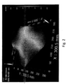
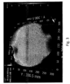
- Figures 2 and 3 are interferometer images that show these elevation deviations in gray scale as a function of location or position on the surface.
- Figure 2 shows the targeted spatial frequencies that need to be removed, that is, reduced in elevation error.
- Figure 3 shows the same part as in Figure 2 with a low spatial frequency removed. That is, errors of a long periodicity or long wavelength (on the order of the diameter of the surface) have been removed; the overall flatness of the surface has been improved. This region is where some applications are the most sensitive.
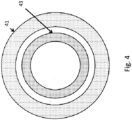
- FIG. 4 what is shown is a top view of a drawing showing concentric tools of different diameter, each independently configured with pressure to float over surface to fulfill a specific function, shape, flatten or roughen for example.
- flattening will be performed before roughening, and will typically involve a greater amount of material being removed than does roughening.
- This illustration depicts the outer concentric tool 41 performing the flattening operation, and the inner concentric tool 43 performing the roughening operation.
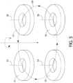
- Figure 5 depicts a top view of a drawing of a plurality of treatment tools 51, 53, 55, 57 arranged in non-concentric fashion.
- the arrangement is termed a "cluster", showing two or more tools that are non concentric performing independent actions of shaping of different spatial frequency ranges or texturing (roughening/smoothing).
- the cluster is mounted to a rotatable shaft ⁇ ("theta") that rotates on its longitudinal axis, termed the "theta" axis.
- Each tool is mounted to an axis 52, 54, 56, 58, which do not have to be parallel to one another, but are each attached to central axis ⁇ .
- Rotation of the cluster allows the action to appear as one larger tool head moving along path 59 with a designed function by the sum of the independent members of the cluster. All tools are free to "float" (conformally) on the surface, for example, by being minimally constrained in their attachment to their respective axes, for instance, by means of a ball-and-socket joint.
- This example demonstrates a localized roughness change, and is made with reference to Figures 6A and 6B .
- Figure 6A is an optical photomicrograph of a ground and polished composite material flat surface prior to its treatment with a tool to deterministically roughen the surface. Both the treatment tool and the surface being processed have about the same hardness and each is fabricated from reaction bonded SiC (RBSC).
- RBSC reaction bonded SiC
- the treatment tool is 27 mm in diameter. By outward appearance, it is a disc, but in reality it has a slight toroidal shape so that when it is brought into contact with the flat surface, the area of contact is not that of a disc but instead is a circle or annulus.
- a dead weight loading of at least 150 grams is applied to the treatment tool. The tool is moved across the surface to be treated at a velocity in the range of 20-50 mm/sec.
- Figure 6B is an optical photomicrograph of the same region of the ground and polished RBSC composite material flat surface of Figure 6A , but following its treatment with the treatment tool operating in surface roughening mode.
- the three black arrows in each photomicrograph point to specific SiC grains. By comparing the appearance of the SiC grains near the tops of corresponding arrows, one can see changes in the grains. These changes are gouges or pits introduced into the grains as a result of the motion of the treatment tool over the flat surface.
- this Example shows that the treatment tool of the disclosure can be used in a mode to impart localized surface roughness to a target surface being treated.
Description
- The present disclosure relates to the use of a unique treatment tool in a deterministic manner for grinding, lapping, polishing or roughening the surface of a work piece such as a chuck for supporting semiconductor wafers.
- Chucks, such as pin chucks, are used to hold flat components for processing. The most common use is to hold wafers (Si, SiC, GaAs, GaN, Sapphire, other) during processing to yield a semiconductor device. Other uses include holding substrates during the fabrication of flat panel displays, solar cells and other such manufactured products. These chucking components are known by many names, including wafer chucks, wafer tables, wafer handling devices, etc.
- The use of pins on these devices is to provide minimum chuck-to-substrate contact. Minimum contact reduces contamination and enhances the ability to maintain high flatness. The pin tops need to have low wear in use to maximize life and precision. The pin tops also need to possess low friction so the substrate easily slides on and off, and lies flat on the pins.
- A pin chuck consists of a rigid body with a plurality of pins on the surface on which the substrate to be processed (e.g., Si wafer) rests. The pins exist in many geometries, and go by many names including burls, mesas, bumps, proud lands, proud rings, etc.
- Regardless of whether the chuck is of the "pin" type or not, the surface that supports whatever is to be chucked (e.g., a semiconductor wafer) needs to be flat to a very high degree of precision. In the case of semiconductor lithography, the flatness is measured in nanometers (nm).
- Methods of flattening are often limited by the flatness of the equipment used such as a flat lap or over arm configuration. With harder and harder materials like ceramics, and in particular SiC and reaction bonded SiC (sometimes referred to here as "RBSC" or "RBSiC"), the uniformity of the lap conditions tend to dominate the cause for non uniformity. These conditions are properties like media, swarf (e.g., contamination or debris), velocity and pressure distribution.
- There are common techniques to deterministically correct for the errors by using a smaller tool and generating a mathematical "hit" map to locally remove more or less material. Some techniques for this deterministic correction include, but not limited to, Ion Beam Figuring (IBF), Magneto Rheological Finishing (MRF), and computer controlled polishing (CCP). As used herein, the phrase "deterministic correction" means that figure, elevation or roughness data as measured for example, by an interferometer or profilometer, is fed into a finishing machine such as a lapping machine, and the machine processes only those areas of the work piece that are in error and need processing (e.g., grinding, lapping or texturing). The machine does not automatically treat the entire surface of the work piece.
- For tools, particularly used in semiconductor handling, the flatness is critical; however, unlike optical surfaces, which require control of a wide range of spatial frequencies, these applications require control over only a narrow range of spatial frequencies.
- The issue with using known deterministic techniques is the tool size is often fixed over a narrow range of spatial frequencies (<10mm), and the tool needs to be traversed over a substantially large substrate (450mm), thus consuming massive amounts of processing and machining time.
- The disclosure addresses these issues, and provides a solution.
-
US 6 179 695 B1 discloses a chemical mechanical polishing apparatus and method for precisely and efficiently polishing a substrate such as a wafer or the like. According to one aspect, the disclosure relates to the apparatus for polishing the surface of an object while supplying an abrasive between the surface to be polished and a polishing surface of a polishing tool brought in contact with the surface to be polished with a predetermined polishing pressure. The polishing tool includes a multiplex ring-shaped pad including a plurality of coaxially disposed ring-shaped polishing pads having different diameters, and coaxially disposed cylindrical shafts for holding corresponding ones of the plurality of ring-shaped polishing pads. Furthermore, by arranging the system such that the rotation speed and the processing pressure of each of the plurality of polishing tools can be changed, if a local defect, such as a projection or the like, is present on the surface to be polished of the substrate, the rotation speed or the processing pressure of a polishing tool contacting the defect portion can be set to be greater than the rotation speeds of other polishing tools. As such, the polished surface of the substrate can be uniformly flattened. Figure 11 ofUS 6 179 695 B1 shows a driving mechanism for moving the surface of the object to be polished relative to the multiplex ring-shaped pad for the rotating table. The polishing tool unit is brought into contact with a part of the surface of the wafer, so that the surface to be polished can be entirely or partially polished using the polishing tool unit in contact with the surface to be polished. Alternatively, by providing the driving mechanism for the multiplex ring-shaped pad and moving the multiplex ring-shaped pad, the surface to be polished can be entirely or partially polished. -
US 2003/045208 A1 discloses a chemical mechanical polishing method and system using retractable polishing pads. Figure 2A ofUS 2003/045208 A1 shows four polishing pads. Each polishing pad is coupled to a respective spindle at end of spindle. Each polishing pad rotates with respect to a central axis of its respective spindle in directions generally indicated by arrows. Polishing pads are extended or retracted along central axes in directions generally indicated by arrows. Such movement brings polishing pads into contact with silicon wafer. Technical advantages of particular embodiments of this disclosure include a chemical mechanical polishing device that allows for the polishing of a silicon wafer by multiple polishing pads at one time. Each polishing pad may isolate and polish a particular area of the silicon wafer. -
WO 2015/002199 A1 discloses a polishing pad, and especially one for polishing the back surface of a semiconductor wafer. The polishing pad comprises a resin-impregnated polishing cloth having a polishing cloth base impregnated with a resin and silicon carbide. - Aspects of the invention are set out in the independent claims.
- In a deterministic setting for finishing the support surface of a chuck such as a wafer chuck, the treatment tool may have a contacting surface configured such that when this contacting or treatment surface is brought into contact with a flat surface, for example, of that of a wafer chuck, the are of contact may be in the form of a circle, ring, or annulus. Thus, the contacting surface of the treatment tool may be slightly toroid-shaped, even though it may appear flat using a mere visual inspection. The treatment tool may have about the same hardness as the work piece (e.g., the wafer chuck) that is being finished. In one embodiment, the treatment tool, or at least the contacting surface, is made from silicon carbide (SiC), or contains SiC, for example, in the form of a composite material such as reaction-bonded SiC.
- Embodiments of the disclosure provide for a method for finishing the support surface of a chuck according to
claim 1. -
-
Figure 1 is a power spectral density plot showing the reduction in amplitude of the spatial frequencies nominally associated with an annular tool of 18mm diameter. -
Figure 2 : This figure shows a typical part with global curvature in predominately the form of a sphere and saddle shape. These are the features that need to be eliminated. -
Figure 3 : This shows the same part as inFigure 2 with a low spatial frequency removed. This region is where some applications are the most sensitive. -
Figure 4 : Diagram showing concentric tools of different diameter, each independently configured with pressure to float over surface to fulfill a specific function: shape, flatten or roughen for example. -
Figure 5 : An option showing a cluster of two or more tools that are non-concentric performing independent actions of shaping of different spatial frequency ranges or texturing (roughening/smoothing). Rotation of the cluster allows the action to appear as one larger tool head with a designed function by the sum of the independent members of the cluster. All tools are free to float on the surface. -
Figures 6A and 6B are optical photomicrographs of a ground and polished reaction bonded silicon carbide flat surface before and after treatment with a tool operated in "surface roughening" mode. - In a first aspect of the disclosure, a novel treatment tool is used in a deterministic manner to process (e.g., grind, lap, polish, roughen or clean) a work piece such as the support surface of a wafer chuck. The treatment tool features a surface of uniform elevation configured to contact and abrade the surface of the work piece as the treatment tool passes over it. The treatment tool may have about the same hardness as the work piece. Visually, the treatment tool may have the appearance of a disc. Alternatively, it may appear as an annulus, ring or toroid. If shaped as an annulus or ring or toroid, the space inside or within the annular space may contain a second treatment tool. Further, the treatment tool may feature a plurality of rings or toroids gathered or assembled together, and collectively defining a common flat surface.
- In one embodiment, the treatment tool is 27 mm in diameter. Visually, the contact surface appears to be a flat disc, but in reality it has a slight toroidal shape so that when it is brought into contact with the flat surface, the area of contact is not that of a disc but instead is a circle or annulus.
- The same treatment tool may be used in cleaning, profiling and roughening modes, depending upon how the tool is used. For example, given a 27mm diameter tool fabricated from reaction bonded silicon carbide, for cleaning debris off of a wafer chuck of similar hardness, a dead weight loading of 5-50 grams, and a tool velocity of 5-30 mm/sec may be used. For profiling (e.g., flattening) a surface, the loading may be 100-175 grams, and the tool velocity may be 20-50 mm/sec. For imparting surface roughness, the tool loading may be in excess of 150 grams, and the tool velocity relative to the surface being processed may be 20-50 mm/sec.
- The treatment tool may be provided in different sizes (diameter or effective diameter), depending on the size of the features or region on the work piece to be processed. For example, a smaller diameter treatment tool (for example, about 10 mm) may be used to treat recessed regions on a wafer chuck, such as the vacuum seal ring on a vacuum chuck.
- According to a first aspect of the disclosed method for mechanically finishing the support surface of a chuck, instead of a single treatment tool having a flat operating or processing surface, a plurality of such treatment tools are provided. At least two, and typically all of the tools of the plurality are used simultaneously. The tools process the support surface mechanically, that is, by removing material via abrasion. The tools may be moved as a group. Each tool is allowed to "float" on the surface, that is, to seek its own conformity with the surface. The pressure that each tool applies against the support surface may be controlled independently of the other tools in the plurality. The tool, or at least the flat surface of the tool, may be shaped as a ring or annulus. Tools may be arranged concentrically, that is, along a common axis that is normal to the flat surface. Tools may also be arranged as a cluster, with no common axis that is normal to the flat surface. The processing of the support surface may be performed deterministically, that is, by programming the finishing to respond to a "hit" map of the elevation or roughness/smoothness of the support surface.
- According to a second aspect of the disclosure, a treatment tool is used in a deterministic environment. According to the invention, the treatment tool (i) is smaller in diameter or 'effective diameter" than the diameter of the work piece (e.g., wafer chuck), and (ii) shaped as a toroid, or having a surface configured to physically contact the work piece that is ring or annulus-shaped.
- According to a third aspect of the disclosure, a treatment tool is used in a deterministic environment, with the treatment tool having a surface configured to physically contact the work piece, with that contacting surface having a hardness that is about the same as the hardness of the work piece surface. In one embodiment, the treatment tool, or at least the flat contacting surface, is made from silicon carbide (SiC), or contains SiC, for example, in the form of a composite material such as reaction-bonded SiC.
- In a deterministic setting or environment, the treatment tool is part of a machine. The machine receives data or information from an instrument such as an interferometer or profilometer. The data may be "figure" or elevation, or surface roughness information, expressed as a function of location on the surface of the chuck. This form of the data may be mathematically derived using the tool foot print or influence into a "hit map", as it shows which locations are too high or too low or of the wrong surface roughness, and therefore it indicates to the machine which regions need to be processed by the treatment tool. The machine may then instruct the treatment tool to process those regions necessary to achieve the desired figure and roughness. The hit map may permit the machine to ignore regions on the chuck that do not require attention, thereby saving time.
- The disclosure embodiments will now be further described with specific reference to the attached drawings.
- Referring first to
Figure 1 , what is shown is a plot of Power Spectral Density as a function of Spatial Frequency. Power Spectral Density is a measure of the amplitude of the deviations from the intended or desired elevation or profile of a surface. Spatial Frequency is a measure of the periodicity of these deviations; that is, how often do they occur in a given distance. What is plotted is elevation data for a surface before and after mechanical finishing treatment. That the "after" curve is below the "before" curve indicates that the deviations in elevation are being reduced; that is, the profile of the surface is closer to what is desired. In this case, flatness is desired, and the treatment shows that the work piece is getting flatter. - A lower power spectral density is desirable, which for this example, demonstrates that the part is getting flatter. The periods where the change occurred is nominally in and about 18 mm and smaller, corresponding to a spatial frequency of about 0.06 (cycle) per mm (or 0.06 1/mm).
-
Figures 2 and3 are interferometer images that show these elevation deviations in gray scale as a function of location or position on the surface.Figure 2 shows the targeted spatial frequencies that need to be removed, that is, reduced in elevation error.Figure 3 shows the same part as inFigure 2 with a low spatial frequency removed. That is, errors of a long periodicity or long wavelength (on the order of the diameter of the surface) have been removed; the overall flatness of the surface has been improved. This region is where some applications are the most sensitive. - Referring now to
Figure 4 , what is shown is a top view of a drawing showing concentric tools of different diameter, each independently configured with pressure to float over surface to fulfill a specific function, shape, flatten or roughen for example. Here, flattening will be performed before roughening, and will typically involve a greater amount of material being removed than does roughening. This illustration depicts the outerconcentric tool 41 performing the flattening operation, and the innerconcentric tool 43 performing the roughening operation. -
Figure 5 depicts a top view of a drawing of a plurality oftreatment tools axis path 59 with a designed function by the sum of the independent members of the cluster. All tools are free to "float" (conformally) on the surface, for example, by being minimally constrained in their attachment to their respective axes, for instance, by means of a ball-and-socket joint. - The disclosure will now be further described with reference to the following Example.
- This example demonstrates a localized roughness change, and is made with reference to
Figures 6A and 6B . -
Figure 6A is an optical photomicrograph of a ground and polished composite material flat surface prior to its treatment with a tool to deterministically roughen the surface. Both the treatment tool and the surface being processed have about the same hardness and each is fabricated from reaction bonded SiC (RBSC). - The treatment tool is 27 mm in diameter. By outward appearance, it is a disc, but in reality it has a slight toroidal shape so that when it is brought into contact with the flat surface, the area of contact is not that of a disc but instead is a circle or annulus. A dead weight loading of at least 150 grams is applied to the treatment tool. The tool is moved across the surface to be treated at a velocity in the range of 20-50 mm/sec.
-
Figure 6B is an optical photomicrograph of the same region of the ground and polished RBSC composite material flat surface ofFigure 6A , but following its treatment with the treatment tool operating in surface roughening mode. The three black arrows in each photomicrograph point to specific SiC grains. By comparing the appearance of the SiC grains near the tops of corresponding arrows, one can see changes in the grains. These changes are gouges or pits introduced into the grains as a result of the motion of the treatment tool over the flat surface. - Thus, this Example shows that the treatment tool of the disclosure can be used in a mode to impart localized surface roughness to a target surface being treated.
- Although much of the forgoing discussion has focused on articles and devices for chucking semiconductor wafers, one of ordinary skill in the art will recognize other related applications where the techniques and articles disclosed in the instant patent application will be useful, for example, in other aspects of semiconductor wafer handling such as Vacuum Wafer Chucks, Wafer Arms, End Effectors, Retical Clamps and Susceptors.
- What is proposed is to use mechanical techniques to flatten one or more narrow band of spatial frequencies using one or more tools, which may be annular or ring-shaped or toroidal. The ability to use several tools simultaneously allows for dramatic reduction in machining time.
- Expanding a little further on this last point, in this aspect of the disclosure where multiple tools are used simultaneously, since the applied pressure on each tool can be independently controlled, and since pressure is highly relevant to the mode in which the tool operates, e.g., cleaning versus profiling versus roughening, one tool can be loaded so as to perform in one mode, e.g., cleaning, while another tool is loaded to perform in a different mode, e.g., flattening or profiling. It may also be possible to differentiate modes of operation based upon velocity of the tool relative to the surface being treated. For example, in the embodiment in which treatment tools are arranged concentrically, if the tools are rotating with the same angular velocity, the outer tool will trace out a larger circumference than will the inner tool; thus, its surface velocity will be greater than that of the inner tool.
Claims (15)
- A method for finishing the support surface of a chuck, comprising:(a) providing a plurality of treatment tools each comprising a surface configured to contact and pass over said support surface, said configured surface comprising a slightly toroidal shape and being configured such that when the configured surface is brought into contact with a flat surface, the area of contact is in the form of a circle;(b) contacting said slightly toroidal shaped surface of each of said treatment tools to said support surface; and(c) flattening said support surface with a first one of said plurality of treatment tools and roughening said support surface with a second one of said plurality of treatment tools by moving the first and second ones of said plurality of treatment tools at independent applied pressures over at least a portion of said chuck support surface to be finished;(d) wherein said applied pressure of each of said plurality of treatment tools against said support surface is independent of that of the others of said plurality of treatment tools, and controllable;(e) and further wherein a diameter of said support surface is larger than an effective diameter of said plurality of treatment tools.
- The method of claim 1, wherein said plurality of treatment tools are arranged concentrically (41, 43).
- The method of claim 1, wherein said plurality of treatment tools are arranged as a cluster (51, 53, 55, 57) that do not share a common axis (52, 54, 56, 58) that is normal to said flat surface.
- The method of claim 1, wherein said moving comprises removing material from said support surface to engineer an elevation of said support surface to a desired profile.
- The method of claim 1, wherein said moving comprises removing material from said support surface to engineer a desired roughness or smoothness of said support surface.
- The method of claim 4 or claim 5, wherein said removing of material is performed deterministically.
- A method for finishing the support surface of a chuck, comprising: providing a machine comprising a plurality of treatment tools according to claim 1; providing information to said machine concerning one or more regions on the support surface that require correction; whereby said machine uses said inputted information to treat substantially only those regions of said support surface that require correction.
- The method of claim 7, wherein said correction comprises cleaning said support surface.
- The method of claim 7, wherein each of said treatment tools has about the same hardness as said support surface.
- The method of claim 7, wherein said inputted information instructs said machine to correct a figure or elevation of said region.
- The method of claim 7, wherein said inputted information instructs said machine to correct a texture of said region.
- The method of claim 7, wherein said surface configured to contact said support surface comprises SiC.
- The method of claim 7, further comprising: simultaneously moving at least two of said plurality of treatment tools at an applied pressure over at least a portion of said chuck support surface to be finished.
- The method of claim 1 or claim 7, wherein the or each treatment tool is attached to the or a machine by a minimally constrained attachment such that said configured surface of said treatment tool is configured to conformally contact said support surface.
- The method of claim 14, wherein said minimally constrained attachment comprises a ball-and-socket joint.
Applications Claiming Priority (2)
| Application Number | Priority Date | Filing Date | Title |
|---|---|---|---|
| US201562205643P | 2015-08-14 | 2015-08-14 | |
| PCT/US2016/046335 WO2017030867A2 (en) | 2015-08-14 | 2016-08-10 | Method for deterministic finishing of a chuck surface |
Publications (3)
| Publication Number | Publication Date |
|---|---|
| EP3334564A2 EP3334564A2 (en) | 2018-06-20 |
| EP3334564A4 EP3334564A4 (en) | 2019-07-17 |
| EP3334564B1 true EP3334564B1 (en) | 2023-11-15 |
Family
ID=58050895
Family Applications (1)
| Application Number | Title | Priority Date | Filing Date |
|---|---|---|---|
| EP16837526.9A Active EP3334564B1 (en) | 2015-08-14 | 2016-08-10 | Method for deterministic finishing of a chuck surface |
Country Status (4)
| Country | Link |
|---|---|
| US (1) | US10953513B2 (en) |
| EP (1) | EP3334564B1 (en) |
| JP (1) | JP7032307B2 (en) |
| WO (1) | WO2017030867A2 (en) |
Families Citing this family (3)
| Publication number | Priority date | Publication date | Assignee | Title |
|---|---|---|---|---|
| EP3334560B1 (en) * | 2015-08-14 | 2023-09-13 | M Cubed Technologies Inc. | Method for removing contamination from a chuck surface |
| CN111699439A (en) * | 2018-02-06 | 2020-09-22 | Asml荷兰有限公司 | Systems, devices, and methods for repairing a substrate support |
| US20210263418A1 (en) * | 2018-07-27 | 2021-08-26 | Asml Netherlands B.V. | Tool for modifying a support surface |
Family Cites Families (37)
| Publication number | Priority date | Publication date | Assignee | Title |
|---|---|---|---|---|
| JPH06252113A (en) * | 1993-02-26 | 1994-09-09 | Matsushita Electric Ind Co Ltd | Method for flattening semiconductor substrate |
| JPH07171747A (en) | 1993-12-21 | 1995-07-11 | Ricoh Co Ltd | Grinding and polishing device |
| JPH0936070A (en) | 1995-07-21 | 1997-02-07 | Nippon Steel Corp | Polishing device of semiconductor wafer |
| JP3664188B2 (en) * | 1995-12-08 | 2005-06-22 | 株式会社東京精密 | Surface processing method and apparatus |
| JP3850924B2 (en) * | 1996-02-15 | 2006-11-29 | 財団法人国際科学振興財団 | Chemical mechanical polishing apparatus and chemical mechanical polishing method |
| JPH1071562A (en) * | 1996-05-10 | 1998-03-17 | Canon Inc | Mechano-chemical polishing device and method |
| KR100264228B1 (en) * | 1996-05-10 | 2000-12-01 | 미다라이 후지오 | Chemical mechanical polishing apparatus and method |
| US6162112A (en) * | 1996-06-28 | 2000-12-19 | Canon Kabushiki Kaisha | Chemical-mechanical polishing apparatus and method |
| JPH11138426A (en) * | 1997-11-11 | 1999-05-25 | Tokyo Electron Ltd | Polishing device |
| JP2968784B1 (en) * | 1998-06-19 | 1999-11-02 | 日本電気株式会社 | Polishing method and apparatus used therefor |
| US6439986B1 (en) | 1999-10-12 | 2002-08-27 | Hunatech Co., Ltd. | Conditioner for polishing pad and method for manufacturing the same |
| JP3859937B2 (en) | 2000-06-02 | 2006-12-20 | 住友大阪セメント株式会社 | Electrostatic chuck |
| US6991524B1 (en) * | 2000-07-07 | 2006-01-31 | Disc Go Technologies Inc. | Method and apparatus for reconditioning digital discs |
| US20030045208A1 (en) * | 2001-09-06 | 2003-03-06 | Neidrich Jason M. | System and method for chemical mechanical polishing using retractable polishing pads |
| US20040116058A1 (en) * | 2002-12-13 | 2004-06-17 | Eastman Kodak Company | Sub-aperture compliant toroidal polishing element |
| US7118446B2 (en) * | 2003-04-04 | 2006-10-10 | Strasbaugh, A California Corporation | Grinding apparatus and method |
| US7150677B2 (en) | 2004-09-22 | 2006-12-19 | Mitsubishi Materials Corporation | CMP conditioner |
| JP4756583B2 (en) | 2005-08-30 | 2011-08-24 | 株式会社東京精密 | Polishing pad, pad dressing evaluation method, and polishing apparatus |
| JP5099476B2 (en) | 2006-12-28 | 2012-12-19 | 株式会社ニコン | Cleaning apparatus and cleaning system, pattern forming apparatus, cleaning method and exposure method, and device manufacturing method |
| JP5018249B2 (en) | 2007-06-04 | 2012-09-05 | 株式会社ニコン | Cleaning device, cleaning method, exposure apparatus, and device manufacturing method |
| JP2009060035A (en) | 2007-09-03 | 2009-03-19 | Shinko Electric Ind Co Ltd | Electrostatic chuck member, its manufacturing method, and electrostatic chuck apparatus |
| JP2009160700A (en) | 2008-01-08 | 2009-07-23 | Disco Abrasive Syst Ltd | Polishing device |
| TWI475594B (en) | 2008-05-19 | 2015-03-01 | Entegris Inc | Electrostatic chuck |
| CN102084466B (en) | 2008-07-01 | 2013-09-11 | 应用材料公司 | Modular base-plate semiconductor polisher architecture |
| JP2010153407A (en) | 2008-12-23 | 2010-07-08 | Nikon Corp | Cleaning method and device, and exposure method and device |
| US8588956B2 (en) | 2009-01-29 | 2013-11-19 | Tayyab Ishaq Suratwala | Apparatus and method for deterministic control of surface figure during full aperture polishing |
| NL2004153A (en) | 2009-02-24 | 2010-08-25 | Asml Netherlands Bv | Lithographic apparatus, a method for removing material of one or more protrusions on a support surface, and an article support system. |
| US20100330890A1 (en) | 2009-06-30 | 2010-12-30 | Zine-Eddine Boutaghou | Polishing pad with array of fluidized gimballed abrasive members |
| JP2012028697A (en) * | 2010-07-27 | 2012-02-09 | Toshiba Corp | Device and method for cleaning |
| US10035237B2 (en) * | 2011-11-02 | 2018-07-31 | The Boeing Company | Robotic end effector including multiple abrasion tools |
| CN109298602B (en) | 2012-02-03 | 2021-10-15 | Asml荷兰有限公司 | Substrate holder and lithographic apparatus |
| JP6085152B2 (en) | 2012-11-22 | 2017-02-22 | 日本特殊陶業株式会社 | Vacuum chuck |
| JP6324958B2 (en) * | 2013-07-02 | 2018-05-16 | 富士紡ホールディングス株式会社 | Polishing pad and manufacturing method thereof |
| JP6109010B2 (en) * | 2013-08-14 | 2017-04-05 | 株式会社ディスコ | Grinding equipment |
| JP2014128877A (en) | 2014-03-03 | 2014-07-10 | Femutekku:Kk | Surface processing apparatus and method |
| US10875153B2 (en) * | 2014-10-17 | 2020-12-29 | Applied Materials, Inc. | Advanced polishing pad materials and formulations |
| JP2017537480A (en) | 2014-11-23 | 2017-12-14 | エム キューブド テクノロジーズM Cubed Technologies | Manufacture and repair of wafer pin chuck |
-
2016
- 2016-08-10 JP JP2018507627A patent/JP7032307B2/en active Active
- 2016-08-10 US US15/568,424 patent/US10953513B2/en active Active
- 2016-08-10 WO PCT/US2016/046335 patent/WO2017030867A2/en active Application Filing
- 2016-08-10 EP EP16837526.9A patent/EP3334564B1/en active Active
Also Published As
| Publication number | Publication date |
|---|---|
| JP7032307B2 (en) | 2022-03-08 |
| EP3334564A4 (en) | 2019-07-17 |
| EP3334564A2 (en) | 2018-06-20 |
| WO2017030867A3 (en) | 2017-03-30 |
| US20180154496A1 (en) | 2018-06-07 |
| WO2017030867A2 (en) | 2017-02-23 |
| JP2018525834A (en) | 2018-09-06 |
| US10953513B2 (en) | 2021-03-23 |
Similar Documents
| Publication | Publication Date | Title |
|---|---|---|
| US10242905B2 (en) | Wafer pin chuck fabrication and repair | |
| US11623319B2 (en) | Machine for finishing a work piece, and having a highly controllable treatment tool | |
| JP5402391B2 (en) | Method for processing synthetic quartz glass substrate for semiconductor | |
| JP2018531503A6 (en) | Machine with highly controllable processing tools for finishing workpieces | |
| EP3334564B1 (en) | Method for deterministic finishing of a chuck surface | |
| KR101908359B1 (en) | Double-headed grinding device and method for double-headed grinding of workpieces | |
| KR20190011677A (en) | Wafer processing method | |
| JP6271339B2 (en) | Grinding and polishing equipment | |
| WO2015182316A1 (en) | Substrate-processing device | |
| EP3334560B1 (en) | Method for removing contamination from a chuck surface | |
| US20220143779A1 (en) | Polishing head with local wafer pressure | |
| US11660721B2 (en) | Dual loading retaining ring | |
| US6821190B1 (en) | Static pad conditioner | |
| JP2001096456A (en) | Polishing head | |
| KR20170087300A (en) | Edge grinding apparatus |
Legal Events
| Date | Code | Title | Description |
|---|---|---|---|
| STAA | Information on the status of an ep patent application or granted ep patent |
Free format text: STATUS: THE INTERNATIONAL PUBLICATION HAS BEEN MADE |
|
| PUAI | Public reference made under article 153(3) epc to a published international application that has entered the european phase |
Free format text: ORIGINAL CODE: 0009012 |
|
| STAA | Information on the status of an ep patent application or granted ep patent |
Free format text: STATUS: REQUEST FOR EXAMINATION WAS MADE |
|
| 17P | Request for examination filed |
Effective date: 20180313 |
|
| AK | Designated contracting states |
Kind code of ref document: A2 Designated state(s): AL AT BE BG CH CY CZ DE DK EE ES FI FR GB GR HR HU IE IS IT LI LT LU LV MC MK MT NL NO PL PT RO RS SE SI SK SM TR |
|
| AX | Request for extension of the european patent |
Extension state: BA ME |
|
| DAV | Request for validation of the european patent (deleted) | ||
| DAX | Request for extension of the european patent (deleted) | ||
| A4 | Supplementary search report drawn up and despatched |
Effective date: 20190619 |
|
| RIC1 | Information provided on ipc code assigned before grant |
Ipc: H01L 21/304 20060101ALI20190613BHEP Ipc: B24B 7/22 20060101AFI20190613BHEP Ipc: B24B 27/00 20060101ALI20190613BHEP Ipc: B24B 37/26 20120101ALI20190613BHEP |
|
| STAA | Information on the status of an ep patent application or granted ep patent |
Free format text: STATUS: EXAMINATION IS IN PROGRESS |
|
| 17Q | First examination report despatched |
Effective date: 20200604 |
|
| STAA | Information on the status of an ep patent application or granted ep patent |
Free format text: STATUS: EXAMINATION IS IN PROGRESS |
|
| STAA | Information on the status of an ep patent application or granted ep patent |
Free format text: STATUS: EXAMINATION IS IN PROGRESS |
|
| GRAP | Despatch of communication of intention to grant a patent |
Free format text: ORIGINAL CODE: EPIDOSNIGR1 |
|
| STAA | Information on the status of an ep patent application or granted ep patent |
Free format text: STATUS: GRANT OF PATENT IS INTENDED |
|
| P01 | Opt-out of the competence of the unified patent court (upc) registered |
Effective date: 20230514 |
|
| INTG | Intention to grant announced |
Effective date: 20230530 |
|
| GRAS | Grant fee paid |
Free format text: ORIGINAL CODE: EPIDOSNIGR3 |
|
| GRAA | (expected) grant |
Free format text: ORIGINAL CODE: 0009210 |
|
| STAA | Information on the status of an ep patent application or granted ep patent |
Free format text: STATUS: THE PATENT HAS BEEN GRANTED |
|
| AK | Designated contracting states |
Kind code of ref document: B1 Designated state(s): AL AT BE BG CH CY CZ DE DK EE ES FI FR GB GR HR HU IE IS IT LI LT LU LV MC MK MT NL NO PL PT RO RS SE SI SK SM TR |
|
| REG | Reference to a national code |
Ref country code: CH Ref legal event code: EP Ref country code: GB Ref legal event code: FG4D |
|
| REG | Reference to a national code |
Ref country code: DE Ref legal event code: R096 Ref document number: 602016084178 Country of ref document: DE |
|
| REG | Reference to a national code |
Ref country code: IE Ref legal event code: FG4D |
|
| REG | Reference to a national code |
Ref country code: NL Ref legal event code: FP |
|
| REG | Reference to a national code |
Ref country code: LT Ref legal event code: MG9D |
|
| PG25 | Lapsed in a contracting state [announced via postgrant information from national office to epo] |
Ref country code: GR Free format text: LAPSE BECAUSE OF FAILURE TO SUBMIT A TRANSLATION OF THE DESCRIPTION OR TO PAY THE FEE WITHIN THE PRESCRIBED TIME-LIMIT Effective date: 20240216 |
|
| PG25 | Lapsed in a contracting state [announced via postgrant information from national office to epo] |
Ref country code: IS Free format text: LAPSE BECAUSE OF FAILURE TO SUBMIT A TRANSLATION OF THE DESCRIPTION OR TO PAY THE FEE WITHIN THE PRESCRIBED TIME-LIMIT Effective date: 20240315 |
|
| PG25 | Lapsed in a contracting state [announced via postgrant information from national office to epo] |
Ref country code: LT Free format text: LAPSE BECAUSE OF FAILURE TO SUBMIT A TRANSLATION OF THE DESCRIPTION OR TO PAY THE FEE WITHIN THE PRESCRIBED TIME-LIMIT Effective date: 20231115 |
|
| REG | Reference to a national code |
Ref country code: AT Ref legal event code: MK05 Ref document number: 1631351 Country of ref document: AT Kind code of ref document: T Effective date: 20231115 |