EP3334539B1 - Transducteurs ultrasonores micro-usinés capacitifs avec augmentation de la sécurité du patient - Google Patents
Transducteurs ultrasonores micro-usinés capacitifs avec augmentation de la sécurité du patient Download PDFInfo
- Publication number
- EP3334539B1 EP3334539B1 EP16750834.0A EP16750834A EP3334539B1 EP 3334539 B1 EP3334539 B1 EP 3334539B1 EP 16750834 A EP16750834 A EP 16750834A EP 3334539 B1 EP3334539 B1 EP 3334539B1
- Authority
- EP
- European Patent Office
- Prior art keywords
- probe
- cmut
- ultrasound
- array probe
- cells
- Prior art date
- Legal status (The legal status is an assumption and is not a legal conclusion. Google has not performed a legal analysis and makes no representation as to the accuracy of the status listed.)
- Active
Links
- 239000000523 sample Substances 0.000 claims description 53
- 238000002604 ultrasonography Methods 0.000 claims description 43
- 239000000758 substrate Substances 0.000 claims description 21
- 239000000872 buffer Substances 0.000 claims description 16
- XUIMIQQOPSSXEZ-UHFFFAOYSA-N Silicon Chemical compound [Si] XUIMIQQOPSSXEZ-UHFFFAOYSA-N 0.000 claims description 4
- 239000003990 capacitor Substances 0.000 claims description 4
- 229910052710 silicon Inorganic materials 0.000 claims description 4
- 239000010703 silicon Substances 0.000 claims description 4
- 239000000853 adhesive Substances 0.000 claims description 2
- 230000001070 adhesive effect Effects 0.000 claims description 2
- 230000003287 optical effect Effects 0.000 claims description 2
- 239000012528 membrane Substances 0.000 description 35
- 210000004027 cell Anatomy 0.000 description 33
- 239000000463 material Substances 0.000 description 9
- 238000000034 method Methods 0.000 description 9
- 238000003384 imaging method Methods 0.000 description 7
- 230000033001 locomotion Effects 0.000 description 7
- 230000017531 blood circulation Effects 0.000 description 6
- 230000008878 coupling Effects 0.000 description 6
- 238000010168 coupling process Methods 0.000 description 6
- 238000005859 coupling reaction Methods 0.000 description 6
- 230000008569 process Effects 0.000 description 6
- 238000002592 echocardiography Methods 0.000 description 5
- 238000011002 quantification Methods 0.000 description 4
- 229910052581 Si3N4 Inorganic materials 0.000 description 3
- 210000004369 blood Anatomy 0.000 description 3
- 239000008280 blood Substances 0.000 description 3
- 210000000170 cell membrane Anatomy 0.000 description 3
- 238000004519 manufacturing process Methods 0.000 description 3
- HQVNEWCFYHHQES-UHFFFAOYSA-N silicon nitride Chemical compound N12[Si]34N5[Si]62N3[Si]51N64 HQVNEWCFYHHQES-UHFFFAOYSA-N 0.000 description 3
- 230000005540 biological transmission Effects 0.000 description 2
- 238000001514 detection method Methods 0.000 description 2
- 238000010586 diagram Methods 0.000 description 2
- 238000005259 measurement Methods 0.000 description 2
- 150000004767 nitrides Chemical class 0.000 description 2
- 230000009467 reduction Effects 0.000 description 2
- 239000004065 semiconductor Substances 0.000 description 2
- 230000035945 sensitivity Effects 0.000 description 2
- 238000000926 separation method Methods 0.000 description 2
- 230000035939 shock Effects 0.000 description 2
- 239000002033 PVDF binder Substances 0.000 description 1
- VYPSYNLAJGMNEJ-UHFFFAOYSA-N Silicium dioxide Chemical compound O=[Si]=O VYPSYNLAJGMNEJ-UHFFFAOYSA-N 0.000 description 1
- 238000009825 accumulation Methods 0.000 description 1
- 210000003484 anatomy Anatomy 0.000 description 1
- 230000008901 benefit Effects 0.000 description 1
- 238000005513 bias potential Methods 0.000 description 1
- 210000000601 blood cell Anatomy 0.000 description 1
- 230000003139 buffering effect Effects 0.000 description 1
- 229910010293 ceramic material Inorganic materials 0.000 description 1
- 238000005229 chemical vapour deposition Methods 0.000 description 1
- 239000003086 colorant Substances 0.000 description 1
- 238000013329 compounding Methods 0.000 description 1
- 238000005336 cracking Methods 0.000 description 1
- 238000002059 diagnostic imaging Methods 0.000 description 1
- 230000000694 effects Effects 0.000 description 1
- 230000008030 elimination Effects 0.000 description 1
- 238000003379 elimination reaction Methods 0.000 description 1
- CWAFVXWRGIEBPL-UHFFFAOYSA-N ethoxysilane Chemical compound CCO[SiH3] CWAFVXWRGIEBPL-UHFFFAOYSA-N 0.000 description 1
- 238000001914 filtration Methods 0.000 description 1
- PCHJSUWPFVWCPO-UHFFFAOYSA-N gold Chemical group [Au] PCHJSUWPFVWCPO-UHFFFAOYSA-N 0.000 description 1
- 239000011810 insulating material Substances 0.000 description 1
- 230000001788 irregular Effects 0.000 description 1
- 238000002955 isolation Methods 0.000 description 1
- 238000004518 low pressure chemical vapour deposition Methods 0.000 description 1
- 230000014759 maintenance of location Effects 0.000 description 1
- 238000001465 metallisation Methods 0.000 description 1
- 210000000056 organ Anatomy 0.000 description 1
- 230000002093 peripheral effect Effects 0.000 description 1
- 238000000623 plasma-assisted chemical vapour deposition Methods 0.000 description 1
- 229910021420 polycrystalline silicon Inorganic materials 0.000 description 1
- 229920000642 polymer Polymers 0.000 description 1
- 229920002981 polyvinylidene fluoride Polymers 0.000 description 1
- 230000001681 protective effect Effects 0.000 description 1
- 230000004044 response Effects 0.000 description 1
- 229910052814 silicon oxide Inorganic materials 0.000 description 1
- 238000004544 sputter deposition Methods 0.000 description 1
- 238000003860 storage Methods 0.000 description 1
- 239000000126 substance Substances 0.000 description 1
- 230000002463 transducing effect Effects 0.000 description 1
- 239000011800 void material Substances 0.000 description 1
- 238000004804 winding Methods 0.000 description 1
Images


Classifications
-
- B—PERFORMING OPERATIONS; TRANSPORTING
- B06—GENERATING OR TRANSMITTING MECHANICAL VIBRATIONS IN GENERAL
- B06B—METHODS OR APPARATUS FOR GENERATING OR TRANSMITTING MECHANICAL VIBRATIONS OF INFRASONIC, SONIC, OR ULTRASONIC FREQUENCY, e.g. FOR PERFORMING MECHANICAL WORK IN GENERAL
- B06B1/00—Methods or apparatus for generating mechanical vibrations of infrasonic, sonic, or ultrasonic frequency
- B06B1/02—Methods or apparatus for generating mechanical vibrations of infrasonic, sonic, or ultrasonic frequency making use of electrical energy
- B06B1/0292—Electrostatic transducers, e.g. electret-type
-
- A—HUMAN NECESSITIES
- A61—MEDICAL OR VETERINARY SCIENCE; HYGIENE
- A61B—DIAGNOSIS; SURGERY; IDENTIFICATION
- A61B8/00—Diagnosis using ultrasonic, sonic or infrasonic waves
- A61B8/12—Diagnosis using ultrasonic, sonic or infrasonic waves in body cavities or body tracts, e.g. by using catheters
-
- A—HUMAN NECESSITIES
- A61—MEDICAL OR VETERINARY SCIENCE; HYGIENE
- A61B—DIAGNOSIS; SURGERY; IDENTIFICATION
- A61B8/00—Diagnosis using ultrasonic, sonic or infrasonic waves
- A61B8/44—Constructional features of the ultrasonic, sonic or infrasonic diagnostic device
- A61B8/4483—Constructional features of the ultrasonic, sonic or infrasonic diagnostic device characterised by features of the ultrasound transducer
-
- G—PHYSICS
- G01—MEASURING; TESTING
- G01N—INVESTIGATING OR ANALYSING MATERIALS BY DETERMINING THEIR CHEMICAL OR PHYSICAL PROPERTIES
- G01N29/00—Investigating or analysing materials by the use of ultrasonic, sonic or infrasonic waves; Visualisation of the interior of objects by transmitting ultrasonic or sonic waves through the object
- G01N29/22—Details, e.g. general constructional or apparatus details
- G01N29/24—Probes
- G01N29/2406—Electrostatic or capacitive probes, e.g. electret or cMUT-probes
-
- B—PERFORMING OPERATIONS; TRANSPORTING
- B06—GENERATING OR TRANSMITTING MECHANICAL VIBRATIONS IN GENERAL
- B06B—METHODS OR APPARATUS FOR GENERATING OR TRANSMITTING MECHANICAL VIBRATIONS OF INFRASONIC, SONIC, OR ULTRASONIC FREQUENCY, e.g. FOR PERFORMING MECHANICAL WORK IN GENERAL
- B06B2201/00—Indexing scheme associated with B06B1/0207 for details covered by B06B1/0207 but not provided for in any of its subgroups
- B06B2201/50—Application to a particular transducer type
- B06B2201/51—Electrostatic transducer
-
- B—PERFORMING OPERATIONS; TRANSPORTING
- B06—GENERATING OR TRANSMITTING MECHANICAL VIBRATIONS IN GENERAL
- B06B—METHODS OR APPARATUS FOR GENERATING OR TRANSMITTING MECHANICAL VIBRATIONS OF INFRASONIC, SONIC, OR ULTRASONIC FREQUENCY, e.g. FOR PERFORMING MECHANICAL WORK IN GENERAL
- B06B2201/00—Indexing scheme associated with B06B1/0207 for details covered by B06B1/0207 but not provided for in any of its subgroups
- B06B2201/70—Specific application
- B06B2201/76—Medical, dental
Definitions
- This invention relates to medical diagnostic ultrasonic imaging and, in particular, to ultrasonic transducer probes which use capacitive micromachined ultrasonic transducers (CMUTs).
- CMUTs capacitive micromachined ultrasonic transducers
- ultrasonic transducers are formed of piezoelectric ceramic materials such as PZT or of piezoelectric polymers such as PVDF. Recently it has been shown that transducers can be made by semiconductor processes. Such transducers are formed of tiny semiconductor cells in which a vibrating membrane generates and receives the ultrasonic energy and are referred to as micromachined ultrasonic transducers (MUTs.) Two such transducer types are those which utilize a piezoelectric material on the membrane called piezoelectric micromachined ultrasonic transducers (PMUTs) and those which utilize a capacitive effect between a conductive membrane and another electrode called capacitive micromachined ultrasonic transducers (CMUTs.) Individual transducer elements may be formed of dozens or hundreds of such MUT cells operating in unison.
- each MUT cell only produces or responds to a small amount of acoustic energy.
- a DC bias voltage is applied across the two electrodes to bias the moving membrane electrode into close proximity with the other electrode. This will enable a relatively smaller signal to vibrate the membrane on transmit, and a small ultrasound signal to develop a relatively large capacitive variation on receive.
- a high DC bias voltage is applied to the moving membrane electrode at the top of the CMUT, and the other electrode on the base of the CMUT is grounded to provide this biasing potential.
- the array is covered with an insulating material such as an acoustic lens which separates the high voltage on the membrane electrodes from the skin of the patient during use of a CMUT ultrasound probe.
- an insulating material such as an acoustic lens which separates the high voltage on the membrane electrodes from the skin of the patient during use of a CMUT ultrasound probe.
- the lens material can become worn during use and can possibly develop surface cracks in the material with age. A crack which is deep enough to reach the membrane electrodes can thus expose the patient to the hazard of a high voltage. Accordingly it is desirable to employ measures which protect the patient from this possible hazard and improve the patient safety of a CMUT probe.
- the bias voltage of an ultrasonic CMUT cell array is applied with a low voltage or ground coupled to the top membrane electrodes of the array and a high voltage coupled to the bottom electrode.
- a control integrated circuit is located below the bottom electrode and the electronics of this circuit is electrically floated relative to the electronics of the ultrasound system to which the CMUT probe is connected.
- a level shifter is used which prevents DC coupling through the signal lines and causes the signals in the probe to be referenced to a floating electrical baseline.
- CMUTs were initially constructed to operate in what is now known as a suspended or "uncollapsed" mode.
- FIGURE 1 a typical uncollapsed CMUT transducer cell 10 is shown in cross-section.
- the CMUT transducer cell 10 is fabricated along with a plurality of similar adjacent cells on a substrate 12 such as silicon.
- a diaphragm or membrane 14 which may be made of silicon nitride is supported above the substrate by an insulating support 16 which may be made of silicon oxide or silicon nitride.
- the cavity 18 between the membrane and the substrate may be air or gas-filled or wholly or partially evacuated.
- a conductive film or layer 20 such as gold forms an electrode on the diaphragm, and a similar film or layer 22 forms an electrode on the substrate. These two electrodes, separated by the dielectric cavity 18, form a capacitance.
- an acoustic signal causes the membrane 14 to vibrate the variation in the capacitance can be detected, thereby transducing the acoustic wave into a corresponding electrical signal.
- an a.c. signal applied across the electrodes 20,22 will modulate the capacitance, causing the membrane to move and thereby transmit an acoustic signal.
- a DC bias voltage V B from a DC bias voltage supply is also applied across the electrodes, drawing the membrane and its top electrode 20 into close proximity with the floor of the cavity of the cell to increase sensitivity.
- FIGURE 2 is a schematic cross-section of a CMUT cell which is operated in the collapsed mode.
- the CMUT cell includes a substrate layer 12 such as silicon, a substrate electrode 22, a membrane layer 14, and a membrane electrode ring 28.
- the electrode 22 is circularly configured and embedded in the substrate layer 12.
- the membrane layer 14 is fixed relative to the top face of the substrate layer 12 and configured/ dimensioned so as to define a spherical or cylindrical cavity 18 between the membrane layer 14 and the substrate layer 12.
- the cell and its cavity 18 may define alternative geometries.
- cavity 18 could define a rectangular and/or square cross-section, a hexagonal cross-section, an elliptical cross-section, or an irregular cross-section.
- the bottom electrode 22 is typically insulated on its cavity-facing surface with an additional layer (not pictured).
- a preferred insulating layer is an oxide-nitride-oxide (ONO) dielectric layer formed above the substrate electrode and below the membrane electrode.
- ONO-dielectric layer advantageously reduced charge accumulation on the electrodes which leads to device instability and drift and reduction in acoustic output pressure.
- the fabrication of ONO-dielectric layers on a CMUT is discussed in detail in European patent application no. 08305553.3 by Klootwijk et al., filed September 16, 2008 and entitled "Capacitive micromachined ultrasound transducer.” Use of the ONO-dielectric layer is desirable with collapsed mode CMUT, which are more susceptible to charge retention than are uncollapsed device.
- the disclosed components may be fabricated from CMOS compatible materials, e . g ., Al, Ti, nitrides (e.g., silicon nitride), oxides (various grades), tetra ethyl oxysilane (TEOS), poly-silicon and the like.
- CMOS compatible materials e . g ., Al, Ti, nitrides (e.g., silicon nitride), oxides (various grades), tetra ethyl oxysilane (TEOS), poly-silicon and the like.
- CMOS compatible materials e . g ., Al, Ti, nitrides (e.g., silicon nitride), oxides (various grades), tetra ethyl oxysilane (TEOS), poly-silicon and the like.
- the oxide and nitride layers may be formed by chemical vapor deposition and the metallization (electrode) layer put down
- Exemplary techniques for producing the disclosed cavity 18 involve defining the cavity in an initial portion of the membrane layer 14 before adding a top face of the membrane layer 14. Other fabrication details may be found in US Pat. 6,328,697 (Fraser ). In the exemplary embodiment depicted in FIGURE 2 , the diameter of the cylindrical cavity 18 is larger than the diameter of the circularly configured electrode plate 22. Electrode ring 28 may have the same outer diameter as the circularly configured electrode plate 22, although such conformance is not required. Thus, in an exemplary embodiment of the present invention, the electrode ring 28 is fixed relative to the top face of the membrane layer 14 so as to align with the electrode plate 22 below.
- the CMUT cell membrane layer is biased to a collapsed state, in which the membrane 14 is in contact with the floor of the cavity 18. This is accomplished by applying a DC bias voltage to the two electrodes as indicated by voltage V B applied to the electrode ring 28 and a reference potential (ground) applied to the substrate electrode 22.
- V B voltage
- V B reference potential
- the bottom electrode is not grounded but coupled to a DC reference potential and the a.c. drive signal for the cell (as well as received signals) are applied to and received at the bottom electrode.
- This electrode arrangement improves patient safety by moving a high voltage potential of the relatively high DC bias voltage further away from the patient-facing side.
- FIGURE 2 illustrates why this is not necessary.
- the center of the membrane is in contact with the floor of the cavity 18.
- the center of the membrane 14 does not move during operation of the CMUT. Rather, it is the peripheral area of the membrane 14 which moves, that which is above the remaining open void of the cavity 18 and below the ring electrode.
- the membrane electrode 28 By forming the membrane electrode 28 as a ring, the charge of the upper plate of the capacitance of the device is located above the area of the CMUT which exhibits the motion and capacitive variation when the CMUT is operating as a transducer.
- the coupling coefficient of the CMUT transducer is improved.
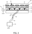
- FIGURE 3 illustrates a CMUT transducer probe 100' connected to an ultrasound system represented at 150 in the drawing. Shown in this illustration is an array of four CMUT cells 10 with a common top electrode 20 and individual bottom electrodes 22 for each CMUT cell. Dielectric 16 supports the top electrodes and membranes across the cavity 18 of each cell which allows the membranes and top electrodes to move in response to an applied DC bias voltage V B and received ultrasonic energy. A DC bias voltage H+ (V B ) is applied to the common electrode 20 to bias the top electrodes in the desired proximity with the floors of the cavities 18.
- V B DC bias voltage
- the exact value of the DC bias voltage required to bring the membrane in the proximity of the cavity floor (into a pre-collapsed or collapsed state) may depend on the CMUT's cell exact design and dimensions.
- the CMUT cells, having an average diameter of about 70 micrometer, may require an application of the DC bias voltage of around 150 V in order to bring the cell membrane in the proximity of the cell floor. Therefore, a range of voltages within which the CMUT array may operate can be a range of the relatively high DC bias voltages being above 50V or even above 100-150V.
- a lens 68 or other insulative covering protects the patient from direct contact with the high voltage of the DC bias.
- the CMUT cells are fabricated on a substrate 70 of an ASIC of control integrated circuitry 72 for the CMUT cells.
- the bottom electrodes 22 of the CMUT cells are electrically connected to the circuitry of the ASIC by vias 74 through the top surface of the substrate 70.
- the CMUT can be formed on its own substrate 12 and connected to a separate ASIC through any of a number of techniques known to those skilled in the art such as flip chip connection, conductive adhesives, or through silicon vias.
- the ASIC circuitry of the CMUT probe is connected to the ultrasound system 150 by a cable 80 which has one end coupled to the ASIC circuitry and the other end coupled by a probe connector to ultrasound system 150.
- the ultrasound system controls the transducer (probe) electronics of the ASIC through analog or digital control lines 82, which transmit control signals to the array, in the cable and receives ultrasound signals through analog or digital signal lines 84, which transmit ultrasound signals from the array.
- the shielding 86 of the cable 80 is coupled to the ASIC so that the reference potential of the ASIC is the same ground reference as that of the ultrasound system.
- FIGURE 3 illustrates the problem addressed by the present invention, which is that a crack 30 has developed in the insulating lens material 68, extending from the patientcontacting upper surface of the lens to the CMUTs below and their top electrodes 20 which are biased to the high voltage H+ suppled from the DC bias voltage supply 140, which is usually around 100 volts. This means that the patient is exposed to the high voltage through the acoustic couplants commonly used with the probe and the hazard of a high voltage shock.
- FIGURE 4 illustrates the same CMUT probe 100' and ultrasound system 150 configuration but with the bias voltage V B applied for improved patient safety in accordance with the present invention.
- a low voltage which does not pose a shock hazard or ground is coupled to the top membrane electrodes as shown in the drawing.
- the high voltage side of the bias potential is then applied at the bottom electrodes of the CMUT cells as shown by the H+ supply 140 connection to the ASIC circuitry 72 (probe electronics).
- the ASIC circuitry 72 probe electronics
- control signals are coupled between the ultrasound system 150 and the ASIC circuitry by level shifters, which provide DC isolation in the control signal lines and shift the signal baseline to that of the electrically floating ASIC circuitry.
- level shifters 90 are used to make the shifted signal coupling through the digital control lines 82, and are also used to couple analog signals such as received ultrasound signals through the signal lines 84.
- level shifters are adapted to shift a baseline of the control signal from a relatively low or reference voltage to a range of the relatively high DC bias voltage, which is coupled to the bottom electrodes of the CMUT cells. Further, these level shifters are adapted to shift a baseline of the ultrasound signals provided by the probe circuitry 72 (ASIC) from the high voltage potential to the range of the relatively low voltage potential (which can be the reference potential of the ultrasound system).
- ASIC probe circuitry 72
- the ASIC electronics 72 is operated by electrically floating it relative to the high potential of the bias voltage, and there is no DC coupling of control through the probe cable 80 to the ASIC electronics, which instead are level shifted to the reference high voltage on the ASIC circuitry.
- the baseline of the ultrasound signals transmitted to the ultrasound system is shifted to the range of the relatively low voltages, within which the system is arranged to operate.
- level shifters provide a further decoupling of the ultrasound system electronics from the high DC voltages of the probe.
- a combination of the level shifters with the floating probes electronics provides not only improved patience safety but also a simplified electrical arrangement.
- the range of the relatively high DC bias voltage has the relatively high DC bias voltage located in its middle and expands into increasing and reduced voltage values with respect to the relatively high DC bias voltage.
- the range can be 25% or 20%, preferably 5% of a total voltage difference between the relatively low (or reference voltage) and the relatively high DC bias voltage.
- the range of the relatively low voltages can be in the order of 5 to 20 V; or 0 to 10 V; while the range of the relatively high DC relatively high DC bias voltage can be 50 to 70 V; or 100 to 160 V.
- the level shifter(s) 90 can be located at the connector end of the probe cable in the connector enclosure, in the handle of the probe, or integrated into the electronics behind the CMUT array as is the ASIC electronics.
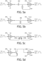
- FIGURES 5a-5d illustrate several level shifter configurations suitable for use for level shifters 90 in FIGURE 4 for shifting the level of digital signals.
- FIGURE 5a shows a pulse from 1.8v digital circuitry being applied to the input of a buffer amplifier 200, which is referenced between 0v for a grounded ultrasound system and a 1.8v supply.
- the output signals of the buffer amplifier are capacitively coupled by a capacitor 204 to the input of a second buffer amplifier 202, which is referenced between 100v and 101.8v.
- the output signals of buffer amplifier 202 are the same as the original input signals, but now referenced to 100v (the voltage of the H+ bias supply in this example) for the 1.8v signal amplitude, which is now at 101.8v.
- This circuit accomplishes level shifting using a capacitor 204.
- FIGURE 5b illustrates another level shifter configuration which uses a transformer 206.
- the primary winding of the transformer is driven by buffer amplifier 200 and the secondary signal is stepped up to a 100v reference level.
- buffer amplifier 202 will again produce the original 1.8v digital pulse but now varying between 101.8v and the 100v reference level.
- FIGURE 5c illustrates an optical level shifter configuration, this one using a pair of photo diodes 208.
- Photo diode 208a is driven by buffer amplifier 200 to emit a pulse of light, which is received by photo diode 208b.
- the electrical signal of receiving photo diode 208b is referenced to 100v by operation of the buffer amplifier 202 referenced between 100v and 101.8v, which is again the amplitude variation of the output signal referenced to 100v.
- FIGURE 5d illustrates another level shifter configuration, this time using a transistor 210 and taking advantage of the high input impedance at the base (with use of a bipolar junction transistor) or gate (with use of a FET) electrode of the transistor.
- the illustrated transistor is driven by the buffer amplifier 200 with its output collector (or drain in the FET case) electrode coupled to the 101.8v supply for buffer amplifier 202.
- the buffer amplifier 202 again produces a 1.8v output signal referenced to 100v (100v ⁇ 101.8v).
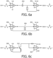
- FIGURES 6a, 6b and 6c illustrate several of the level shifter configurations of FIGURE 5 , this time being used for level shifting an analog signal.
- the input signal is an analog signal varying about a 0.9v reference level.
- the output buffer amplifier 202 produces the same 1.8v peak-to-peak analog signal as the input signal but now baselined to 100.9v, varying between a maximum excursion of 100v and 101.8v in each example.
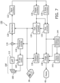
- FIGURE 7 illustrates in block diagram form an ultrasonic diagnostic imaging system 150 suitable for use with a CMUT array probe of the present invention.
- a CMUT array 100 is located on the tip of a catheter or distal end of an ultrasound probe 100', together with a microbeamformer ASIC 112.
- the microbeamformer ASIC 112 may comprise control integrated circuitry 72 for the CMUT cells.
- the CMUT array 100 can be a one- or a twodimensional array of MUT transducer elements capable of scanning in a 2D plane or in three dimensions for 3D imaging.
- Microbeamformers are capable of at least partial beamforming of the signals received by groups or "patches" of transducer elements as described in US Pats. 5,997,479 (Savord et al.
- the microbeamformer is coupled to transmit/receive (T/R) switches 116 which switch between transmission and reception and protect the main system beamformer 120 from high energy transmit signals when a microbeamformer is not used and a transducer array is operated directly by the main system beamformer.
- T/R transmit/receive
- the transmission of ultrasonic beams from the CMUT transducer array 100 under control of the microbeamformer ASIC 112 is directed by a transducer controller 118 coupled to the T/R switch and the main system beamformer 120, which receives input from the user's operation of the user interface or control panel 38.
- the transducer controller 118 also controls a circuit 104 for the DC bias applied from the DC bias supply 140 to the CMUT cells which biases the cell membranes 14 as described above to a partially or fully collapsed state for operation of the CMUTs in the desired mode of operation.
- the partially beamformed signals produced by the microbeamformer 112 on receive are coupled to a main beamformer 120 where partially beamformed signals from individual patches of transducer elements are combined into a fully beamformed signal.
- the main beamformer 120 may have 128 channels, each of which receives a partially beamformed signal from a patch of dozens or hundreds of CMUT transducer cells. In this way the signals received by thousands of transducer elements of a CMUT transducer array can contribute efficiently to a single beamformed signal.
- the acoustic signals received from rows of CMUT cells are processed into beams from an image plane in front of the rows of cells to form a scanned 2D image.
- the beamformed signals are coupled to a signal processor 122.
- the signal processor 122 can process the received echo signals in various ways, such as bandpass filtering, decimation, I and Q component separation, and harmonic signal separation which acts to separate linear and nonlinear signals so as to enable the identification of nonlinear echo signals returned from tissue and microbubbles.
- the signal processor may also perform additional signal enhancement such as speckle reduction, signal compounding, and noise elimination.
- the bandpass filter in the signal processor can be a tracking filter, with its passband sliding from a higher frequency band to a lower frequency band as echo signals are received from increasing depths, thereby rejecting the noise at higher frequencies from greater depths where these frequencies are devoid of anatomical information.
- the processed signals are coupled to a B mode processor 126 and a Doppler processor 128.
- the B mode processor 126 employs amplitude detection for the imaging of structures in the body such as the tissue of organs and vessels in the body.
- B mode images of structure of the body may be formed in either the harmonic mode or the fundamental mode or a combination of both as described in US Pat. 6,283,919 (Roundhill et al. ) and US Pat. 6,458,083 (Jago et al. )
- the Doppler processor 128 processes temporally distinct signals from tissue movement and blood flow for the detection of the motion of substances such as the flow of blood cells in the image field.
- the Doppler processor typically includes a wall filter with parameters which may be set to pass and/or reject echoes returned from selected types of materials in the body.
- the wall filter can be set to have a passband characteristic which passes signal of relatively low amplitude from higher velocity materials while rejecting relatively strong signals from lower or zero velocity material.
- This passband characteristic will pass signals from flowing blood while rejecting signals from nearby stationary or slowing moving objects such as the wall of the heart.
- An inverse characteristic would pass signals from moving tissue of the heart while rejecting blood flow signals for what is referred to as tissue Doppler imaging, detecting and depicting the motion of tissue.
- the Doppler processor receives and processes a sequence of temporally discrete echo signals from different points in an image field, the sequence of echoes from a particular point referred to as an ensemble.
- An ensemble of echoes received in rapid succession over a relatively short interval can be used to estimate the Doppler shift frequency of flowing blood, with the correspondence of the Doppler frequency to velocity indicating the blood flow velocity.
- An ensemble of echoes received over a longer period of time is used to estimate the velocity of slower flowing blood or slowly moving tissue.
- the structural and motion signals produced by the B mode and Doppler processors are coupled to a scan converter 132 and a multiplanar reformatter 144.
- the scan converter arranges the echo signals in the spatial relationship from which they were received into a desired image format. For instance, the scan converter may arrange the echo signal into a two dimensional (2D) sector-shaped format, or a pyramidal three dimensional (3D) image.
- the scan converter can overlay a B mode structural image with colors corresponding to motion at points in the image field corresponding with their Doppler-estimated velocities to produce a color Doppler image which depicts the motion of tissue and blood flow in the image field.
- the multiplanar reformatter will convert echoes which are received from points in a common plane in a volumetric region of the body into an ultrasonic image of that plane, as described in US Pat. 6,443,896 (Detmer ).
- a volume renderer 142 converts the echo signals of a 3D data set into a projected 3D image as viewed from a given reference point as described in US Pat. 6,530,885 (Entrekin et al. )
- the 2D or 3D images are coupled from the scan converter 32, multiplanar reformatter 44, and volume renderer 142 to an image processor 130 for further enhancement, buffering and temporary storage for display on an image display 40.
- the blood flow velocity values produced by the Doppler processor 128 are coupled to a flow quantification processor 134.
- the flow quantification processor produces measure of different flow conditions such as the volume rate of blood flow.
- the flow quantification processor may receive input from the user control panel 38, such as the point in the anatomy of an image where a measurement is to be made.
- Output data from the flow quantification processor is coupled to a graphics processor 136 for the reproduction of measurement values with the image on the display 40.
- the graphics processor 136 can also generate graphic overlays for display with the ultrasound images. These graphic overlays can contain standard identifying information such as patient name, date and time of the image, imaging parameters, and the like. For these purposes the graphics processor receives input from the user interface 38, such as a typed patient name.
- the user interface is also coupled to the transducer controller 118 to control the generation of ultrasound signals from the transducer array 100 and hence the images produced by the transducer array and the ultrasound system.
- the user interface is also coupled to the multiplanar reformatter 144 for selection and control of a display of multiple multiplanar reformatted (MPR) images which may be used to perform quantified measures in the image field of the MPR images.
- MPR multiplanar reformatted
Claims (14)
- Transducteur ultrasonore capacitif micro-usiné, CMUT, sonde en réseau (100') avec une sécurité améliorée pour le patient, ladite sonde (100') pouvant être connectée à un système à ultrasons (150) fonctionnant dans une gamme de tensions relativement basses, dans laquelle ladite sonde (100') comprend:un substrat (70);une pluralité de cellules CMUT (10) situées sur le substrat (70), chaque cellule ayant une électrode supérieure (20) orientée vers le patient et une électrode inférieure (22), une électronique de sonde (72) couplée aux cellules CMUT (10) et conçue pour fournir des signaux de commande aux cellules (10) et des signaux ultrasonores en provenance des cellules (10) ;dans lequel, une tension de référence relativement faible est couplée aux électrodes supérieures (20) des cellules CMUT (10); etune tension de polarisation CC relativement élevée est couplée aux électrodes inférieures (22) des cellules CMUT (10), la tension de polarisation CC relativement élevée étant supérieure à la tension de référence relativement faible;la sonde (100') comprend en outre un câble de sonde (80) ayant une première extrémité couplée à l'électronique de la sonde (72) et une deuxième extrémité pouvant être couplée au système à ultrasons (150) et ayant une ou plusieurs des lignes suivantes une ligne de signal de commande (82) et une ligne de signal ultrasonore (84), dans lequel chaque ligne de signal de commande (82) est adaptée pour transmettre les signaux de commande du système à ultrasons (150) à l'électronique de la sonde (72) et chaque ligne de signal ultrasonore (84) est adaptée pour transmettre les signaux d'ultrasons de l'électronique de la sonde (72) au système à ultrasons (150); etun ou plusieurs décalages de niveau (90) couplés à une ou plusieurs lignes de signal de commande (82) et à une ligne de signal ultrasonore (84), un ou plusieurs décalages de niveau (90) étant adaptés pour déplacer une ligne de base du signal de commande vers une plage de tension de polarisation CC relativement élevée et pour déplacer une ligne de base du signal ultrasonore vers une plage de tensions relativement faibles caractérisé en ce fait que l'électronique de la sonde (72) est conçue pour flotter électriquement à un potentiel de tension élevé de la tension de polarisation continue relativement élevée par rapport au potentiel de masse du système ultrasonore.
- Sonde en réseau CMUT (100') de la revendication 1, dans laquelle le ou les décalages de niveau (90) comprennent en outre un décalage de niveau capacitif, un décalage de niveau de transformateur, un décalage de niveau optique ou un décalage de niveau de transistor.
- Sonde en réseau CMUT (100') selon la revendication 2, dans laquelle l'électronique de la sonde (72) comprend en outre des circuits ASIC.
- Sonde en réseau CMUT (100') selon la revendication 3, dans laquelle le circuit ASIC est situé sur le substrat (70) .
- Sonde en réseau CMUT (100') selon la revendication 3, comprenant en outre un deuxième substrat, dans lequel le circuit ASIC est situé sur le deuxième substrat.
- Sonde en réseau CMUT (100') selon la revendication 5, dans laquelle le circuit ASIC et son substrat sont liés aux cellules CMUT (10) et à leur substrat (70) par une connexion de puce Hip, un adhésif conducteur ou des vias en silicium (74).
- Sonde en réseau CMUT (100') selon la revendication 2, dans laquelle le ou les décalages de niveau (90) comprennent en outre un premier et un deuxième tampons (200, 202) interposés par un condensateur (204), un premier et un deuxième tampons (200, 202) interposés par un transformateur (206), un premier et un deuxième tampons (200, 202) interposés par des photodiodes (208a, 208b), ou un premier et un deuxième tampons (200, 202) interposés par un transistor (210).
- Sonde en réseau CMUT (100') selon la revendication 1, dans laquelle un ou plusieurs décalages de niveau (90) sont situés à la deuxième extrémité du câble (80).
- Sonde en réseau CMUT (100') selon la revendication 1, dans laquelle un ou plusieurs décalages de niveau (90) sont situés dans une poignée de la sonde CMUT (100').
- Sonde en réseau CMUT (100') selon la revendication 9, dans laquelle un ou plusieurs décalages de niveau (90) sont intégrés dans l'électronique de la sonde (72).
- Sonde en réseau CMUT (100') selon la revendication 1, dans laquelle la ligne de signal ultrasonore (84) comprend en outre une ligne de signal analogique.
- Sonde en réseau CMUT (100') selon la revendication 1, dans laquelle la tension de polarisation CC élevée comprend en outre une alimentation de polarisation CC couplée entre l'électronique de la sonde (72) et la masse.
- Sonde en réseau CMUT (100') selon la revendication 1, comprenant en outre un revêtement isolant recouvrant les électrodes supérieures orientées vers le patient (20) de la pluralité de cellules CMUT (10).
- Sonde en réseau CMUT (100') selon la revendication 13, dans laquelle le revêtement isolant comprend en outre une lentille acoustique.
Applications Claiming Priority (3)
| Application Number | Priority Date | Filing Date | Title |
|---|---|---|---|
| US201562203533P | 2015-08-11 | 2015-08-11 | |
| EP15183223 | 2015-09-01 | ||
| PCT/EP2016/069136 WO2017025598A1 (fr) | 2015-08-11 | 2016-08-11 | Transducteurs à ultrasons micro-usinés capacitifs permettant une meilleure sécurité du patient |
Publications (2)
| Publication Number | Publication Date |
|---|---|
| EP3334539A1 EP3334539A1 (fr) | 2018-06-20 |
| EP3334539B1 true EP3334539B1 (fr) | 2023-06-14 |
Family
ID=54072672
Family Applications (1)
| Application Number | Title | Priority Date | Filing Date |
|---|---|---|---|
| EP16750834.0A Active EP3334539B1 (fr) | 2015-08-11 | 2016-08-11 | Transducteurs ultrasonores micro-usinés capacitifs avec augmentation de la sécurité du patient |
Country Status (5)
| Country | Link |
|---|---|
| US (1) | US11213855B2 (fr) |
| EP (1) | EP3334539B1 (fr) |
| JP (2) | JP7094217B2 (fr) |
| CN (1) | CN107921477B (fr) |
| WO (1) | WO2017025598A1 (fr) |
Families Citing this family (3)
| Publication number | Priority date | Publication date | Assignee | Title |
|---|---|---|---|---|
| JP7026111B2 (ja) * | 2016-06-20 | 2022-02-25 | バタフライ ネットワーク,インコーポレイテッド | 微細加工超音波トランスデューサのための電気接点配置 |
| CN109561876A (zh) * | 2018-10-24 | 2019-04-02 | 深圳市汇顶科技股份有限公司 | 超声换能器及其制造方法 |
| US20220313205A1 (en) * | 2021-04-05 | 2022-10-06 | GE Precision Healthcare LLC | Methods and systems for an invasive deployable device |
Family Cites Families (35)
| Publication number | Priority date | Publication date | Assignee | Title |
|---|---|---|---|---|
| US6283919B1 (en) | 1996-11-26 | 2001-09-04 | Atl Ultrasound | Ultrasonic diagnostic imaging with blended tissue harmonic signals |
| US6458083B1 (en) | 1996-11-26 | 2002-10-01 | Koninklijke Philips Electronics N.V. | Ultrasonic harmonic imaging with adaptive image formation |
| US6530887B1 (en) * | 1996-12-24 | 2003-03-11 | Teratech Corporation | Ultrasound probe with integrated electronics |
| US6013032A (en) | 1998-03-13 | 2000-01-11 | Hewlett-Packard Company | Beamforming methods and apparatus for three-dimensional ultrasound imaging using two-dimensional transducer array |
| US5997479A (en) | 1998-05-28 | 1999-12-07 | Hewlett-Packard Company | Phased array acoustic systems with intra-group processors |
| US6530885B1 (en) | 2000-03-17 | 2003-03-11 | Atl Ultrasound, Inc. | Spatially compounded three dimensional ultrasonic images |
| US6443901B1 (en) | 2000-06-15 | 2002-09-03 | Koninklijke Philips Electronics N.V. | Capacitive micromachined ultrasonic transducers |
| US6443896B1 (en) | 2000-08-17 | 2002-09-03 | Koninklijke Philips Electronics N.V. | Method for creating multiplanar ultrasonic images of a three dimensional object |
| US6468216B1 (en) | 2000-08-24 | 2002-10-22 | Kininklijke Philips Electronics N.V. | Ultrasonic diagnostic imaging of the coronary arteries |
| US6583671B2 (en) * | 2000-12-01 | 2003-06-24 | Sony Corporation | Stable AGC transimpedance amplifier with expanded dynamic range |
| JP2007527285A (ja) * | 2004-02-27 | 2007-09-27 | ジョージア テック リサーチ コーポレイション | 多要素電極cmut素子及び製作方法 |
| JP4477631B2 (ja) | 2004-06-11 | 2010-06-09 | オリンパス株式会社 | 超音波プローブ装置及び超音波診断装置 |
| RU2404711C2 (ru) * | 2005-04-25 | 2010-11-27 | Конинклейке Филипс Электроникс Н.В. | Способ и устройство для непрерывной визуализации посредством системы ультразвукового преобразователя |
| US8366616B2 (en) * | 2005-05-09 | 2013-02-05 | Hitachi Medical Corporation | Ultrasonic diagnostic apparatus |
| JP2007244687A (ja) * | 2006-03-16 | 2007-09-27 | Matsushita Electric Ind Co Ltd | 超音波診断装置 |
| WO2008054395A1 (fr) * | 2006-11-03 | 2008-05-08 | Research Triangle Institute | Sondes d'imagerie à ultrasons améliorées utilisant des transducteurs piézoélectriques en mode courbure |
| JP5408935B2 (ja) | 2007-09-25 | 2014-02-05 | キヤノン株式会社 | 電気機械変換素子及びその製造方法 |
| JP5159290B2 (ja) | 2007-12-20 | 2013-03-06 | 株式会社東芝 | 超音波診断装置および超音波プローブ |
| CN102159334A (zh) | 2008-09-16 | 2011-08-17 | 皇家飞利浦电子股份有限公司 | 电容性微机械加工的超声换能器 |
| EP2269746B1 (fr) * | 2009-07-02 | 2014-05-14 | Nxp B.V. | Capteur capacitif en mode réduit |
| US8638148B2 (en) * | 2009-10-07 | 2014-01-28 | Fairchild Semiconductor Corporation | Edge rate control |
| JP5947511B2 (ja) * | 2011-09-08 | 2016-07-06 | キヤノン株式会社 | 電気機械変換装置 |
| WO2014013394A1 (fr) | 2012-07-18 | 2014-01-23 | Koninklijke Philips N.V. | Dispositif d'attaque et procédé d'attaque pour attaquer une charge, en particulier un transducteur à ultrasons |
| US9479162B2 (en) | 2012-11-28 | 2016-10-25 | Analog Devices, Inc. | Apparatus and methods for ultrasound probes |
| US20140257107A1 (en) * | 2012-12-28 | 2014-09-11 | Volcano Corporation | Transducer Assembly for an Imaging Device |
| JP6234073B2 (ja) * | 2013-06-07 | 2017-11-22 | キヤノン株式会社 | 静電容量型トランスデューサの駆動装置、及び被検体情報取得装置 |
| JP5855050B2 (ja) * | 2013-07-10 | 2016-02-09 | キヤノン株式会社 | トランスデューサ、被検体情報取得装置 |
| US9592030B2 (en) | 2013-07-23 | 2017-03-14 | Butterfly Network, Inc. | Interconnectable ultrasound transducer probes and related methods and apparatus |
| CN105492129B (zh) * | 2013-08-27 | 2019-07-02 | 皇家飞利浦有限公司 | 双模式cmut换能器 |
| JP6189167B2 (ja) * | 2013-10-10 | 2017-08-30 | 株式会社日立製作所 | 超音波探触子およびそれを用いた超音波診断装置 |
| WO2016008833A1 (fr) * | 2014-07-16 | 2016-01-21 | Koninklijke Philips N.V. | Puces de transducteurs d'ultrasons micro-usinés capacitifs tuilées avec uniformité de pas |
| WO2016091624A1 (fr) * | 2014-12-11 | 2016-06-16 | Koninklijke Philips N.V. | Dispositif de transducteur d'ultrasons micro-usiné capacitif à deux bornes |
| JP6425994B2 (ja) * | 2014-12-24 | 2018-11-21 | キヤノンメディカルシステムズ株式会社 | 超音波診断装置 |
| JP6472313B2 (ja) * | 2015-04-16 | 2019-02-20 | キヤノン株式会社 | 探触子及び情報取得装置 |
| US20180028150A1 (en) | 2016-07-29 | 2018-02-01 | Canon Kabushiki Kaisha | Ultrasonic probe and subject information acquisition apparatus |
-
2016
- 2016-08-11 CN CN201680046679.5A patent/CN107921477B/zh active Active
- 2016-08-11 US US15/750,604 patent/US11213855B2/en active Active
- 2016-08-11 EP EP16750834.0A patent/EP3334539B1/fr active Active
- 2016-08-11 WO PCT/EP2016/069136 patent/WO2017025598A1/fr active Application Filing
- 2016-08-11 JP JP2018505003A patent/JP7094217B2/ja active Active
-
2022
- 2022-04-28 JP JP2022074781A patent/JP7268223B2/ja active Active
Also Published As
| Publication number | Publication date |
|---|---|
| JP7094217B2 (ja) | 2022-07-01 |
| JP2022105543A (ja) | 2022-07-14 |
| US20190015871A1 (en) | 2019-01-17 |
| JP2018522667A (ja) | 2018-08-16 |
| CN107921477B (zh) | 2020-04-10 |
| WO2017025598A1 (fr) | 2017-02-16 |
| JP7268223B2 (ja) | 2023-05-02 |
| US11213855B2 (en) | 2022-01-04 |
| CN107921477A (zh) | 2018-04-17 |
| EP3334539A1 (fr) | 2018-06-20 |
Similar Documents
| Publication | Publication Date | Title |
|---|---|---|
| US11097312B2 (en) | Capacitive micromachined ultrasonic transducers with increased lifetime | |
| EP2400893B1 (fr) | Cmut pré-affaissé conservant l'affaissement mécanique | |
| JP7268223B2 (ja) | 増大された患者安全性を持つ容量性マイクロマシン超音波トランスデューサ | |
| JP5432467B2 (ja) | 超音波システム用の送受波回路 | |
| US10898924B2 (en) | Tiled CMUT dies with pitch uniformity | |
| US20160199030A1 (en) | Dual mode cmut transducer | |
| CN110997165B (zh) | 电容式微机械超声换能器(cmut)设备和控制方法 | |
| JP2019522925A (ja) | 広帯域超音波トランスジューサ | |
| JP7427027B2 (ja) | 容量性微細加工超音波トランスデューサ(cmut)デバイス | |
| WO2015028945A2 (fr) | Commande de fréquence variable de transducteur cmut à mode effondré | |
| WO2015028949A2 (fr) | Système d'imagerie ultrasonore à transducteur capacitif ultrasonore micro-usiné pour une imagerie à large plage de fréquences | |
| WO2017149421A1 (fr) | Réseau de transducteurs ultrasonores cmut à profondeur de champ améliorée | |
| CN106660072B (zh) | 具有节距均匀性的平铺的cmut切片 | |
| EP3334540B1 (fr) | Transducteurs ultrasonores capacitifs micro-usinés avec protection de surintensité |
Legal Events
| Date | Code | Title | Description |
|---|---|---|---|
| STAA | Information on the status of an ep patent application or granted ep patent |
Free format text: STATUS: THE INTERNATIONAL PUBLICATION HAS BEEN MADE |
|
| PUAI | Public reference made under article 153(3) epc to a published international application that has entered the european phase |
Free format text: ORIGINAL CODE: 0009012 |
|
| STAA | Information on the status of an ep patent application or granted ep patent |
Free format text: STATUS: REQUEST FOR EXAMINATION WAS MADE |
|
| 17P | Request for examination filed |
Effective date: 20180312 |
|
| AK | Designated contracting states |
Kind code of ref document: A1 Designated state(s): AL AT BE BG CH CY CZ DE DK EE ES FI FR GB GR HR HU IE IS IT LI LT LU LV MC MK MT NL NO PL PT RO RS SE SI SK SM TR |
|
| AX | Request for extension of the european patent |
Extension state: BA ME |
|
| DAV | Request for validation of the european patent (deleted) | ||
| DAX | Request for extension of the european patent (deleted) | ||
| RAP1 | Party data changed (applicant data changed or rights of an application transferred) |
Owner name: KONINKLIJKE PHILIPS N.V. |
|
| STAA | Information on the status of an ep patent application or granted ep patent |
Free format text: STATUS: EXAMINATION IS IN PROGRESS |
|
| 17Q | First examination report despatched |
Effective date: 20210507 |
|
| STAA | Information on the status of an ep patent application or granted ep patent |
Free format text: STATUS: EXAMINATION IS IN PROGRESS |
|
| GRAP | Despatch of communication of intention to grant a patent |
Free format text: ORIGINAL CODE: EPIDOSNIGR1 |
|
| STAA | Information on the status of an ep patent application or granted ep patent |
Free format text: STATUS: GRANT OF PATENT IS INTENDED |
|
| INTG | Intention to grant announced |
Effective date: 20230119 |
|
| GRAS | Grant fee paid |
Free format text: ORIGINAL CODE: EPIDOSNIGR3 |
|
| GRAA | (expected) grant |
Free format text: ORIGINAL CODE: 0009210 |
|
| STAA | Information on the status of an ep patent application or granted ep patent |
Free format text: STATUS: THE PATENT HAS BEEN GRANTED |
|
| AK | Designated contracting states |
Kind code of ref document: B1 Designated state(s): AL AT BE BG CH CY CZ DE DK EE ES FI FR GB GR HR HU IE IS IT LI LT LU LV MC MK MT NL NO PL PT RO RS SE SI SK SM TR |
|
| REG | Reference to a national code |
Ref country code: CH Ref legal event code: EP |
|
| REG | Reference to a national code |
Ref country code: DE Ref legal event code: R096 Ref document number: 602016080341 Country of ref document: DE |
|
| REG | Reference to a national code |
Ref country code: AT Ref legal event code: REF Ref document number: 1578844 Country of ref document: AT Kind code of ref document: T Effective date: 20230715 |
|
| REG | Reference to a national code |
Ref country code: DE Ref legal event code: R084 Ref document number: 602016080341 Country of ref document: DE |
|
| REG | Reference to a national code |
Ref country code: LT Ref legal event code: MG9D |
|
| REG | Reference to a national code |
Ref country code: NL Ref legal event code: MP Effective date: 20230614 |
|
| PG25 | Lapsed in a contracting state [announced via postgrant information from national office to epo] |
Ref country code: SE Free format text: LAPSE BECAUSE OF FAILURE TO SUBMIT A TRANSLATION OF THE DESCRIPTION OR TO PAY THE FEE WITHIN THE PRESCRIBED TIME-LIMIT Effective date: 20230614 Ref country code: NO Free format text: LAPSE BECAUSE OF FAILURE TO SUBMIT A TRANSLATION OF THE DESCRIPTION OR TO PAY THE FEE WITHIN THE PRESCRIBED TIME-LIMIT Effective date: 20230914 Ref country code: ES Free format text: LAPSE BECAUSE OF FAILURE TO SUBMIT A TRANSLATION OF THE DESCRIPTION OR TO PAY THE FEE WITHIN THE PRESCRIBED TIME-LIMIT Effective date: 20230614 |
|
| PGFP | Annual fee paid to national office [announced via postgrant information from national office to epo] |
Ref country code: GB Payment date: 20230822 Year of fee payment: 8 |
|
| REG | Reference to a national code |
Ref country code: AT Ref legal event code: MK05 Ref document number: 1578844 Country of ref document: AT Kind code of ref document: T Effective date: 20230614 |
|
| PG25 | Lapsed in a contracting state [announced via postgrant information from national office to epo] |
Ref country code: RS Free format text: LAPSE BECAUSE OF FAILURE TO SUBMIT A TRANSLATION OF THE DESCRIPTION OR TO PAY THE FEE WITHIN THE PRESCRIBED TIME-LIMIT Effective date: 20230614 Ref country code: NL Free format text: LAPSE BECAUSE OF FAILURE TO SUBMIT A TRANSLATION OF THE DESCRIPTION OR TO PAY THE FEE WITHIN THE PRESCRIBED TIME-LIMIT Effective date: 20230614 Ref country code: LV Free format text: LAPSE BECAUSE OF FAILURE TO SUBMIT A TRANSLATION OF THE DESCRIPTION OR TO PAY THE FEE WITHIN THE PRESCRIBED TIME-LIMIT Effective date: 20230614 Ref country code: LT Free format text: LAPSE BECAUSE OF FAILURE TO SUBMIT A TRANSLATION OF THE DESCRIPTION OR TO PAY THE FEE WITHIN THE PRESCRIBED TIME-LIMIT Effective date: 20230614 Ref country code: HR Free format text: LAPSE BECAUSE OF FAILURE TO SUBMIT A TRANSLATION OF THE DESCRIPTION OR TO PAY THE FEE WITHIN THE PRESCRIBED TIME-LIMIT Effective date: 20230614 Ref country code: GR Free format text: LAPSE BECAUSE OF FAILURE TO SUBMIT A TRANSLATION OF THE DESCRIPTION OR TO PAY THE FEE WITHIN THE PRESCRIBED TIME-LIMIT Effective date: 20230915 |
|
| PGFP | Annual fee paid to national office [announced via postgrant information from national office to epo] |
Ref country code: DE Payment date: 20230828 Year of fee payment: 8 |
|
| PG25 | Lapsed in a contracting state [announced via postgrant information from national office to epo] |
Ref country code: FI Free format text: LAPSE BECAUSE OF FAILURE TO SUBMIT A TRANSLATION OF THE DESCRIPTION OR TO PAY THE FEE WITHIN THE PRESCRIBED TIME-LIMIT Effective date: 20230614 |
|
| PG25 | Lapsed in a contracting state [announced via postgrant information from national office to epo] |
Ref country code: SK Free format text: LAPSE BECAUSE OF FAILURE TO SUBMIT A TRANSLATION OF THE DESCRIPTION OR TO PAY THE FEE WITHIN THE PRESCRIBED TIME-LIMIT Effective date: 20230614 |
|
| PG25 | Lapsed in a contracting state [announced via postgrant information from national office to epo] |
Ref country code: IS Free format text: LAPSE BECAUSE OF FAILURE TO SUBMIT A TRANSLATION OF THE DESCRIPTION OR TO PAY THE FEE WITHIN THE PRESCRIBED TIME-LIMIT Effective date: 20231014 |
|
| PG25 | Lapsed in a contracting state [announced via postgrant information from national office to epo] |
Ref country code: SM Free format text: LAPSE BECAUSE OF FAILURE TO SUBMIT A TRANSLATION OF THE DESCRIPTION OR TO PAY THE FEE WITHIN THE PRESCRIBED TIME-LIMIT Effective date: 20230614 Ref country code: SK Free format text: LAPSE BECAUSE OF FAILURE TO SUBMIT A TRANSLATION OF THE DESCRIPTION OR TO PAY THE FEE WITHIN THE PRESCRIBED TIME-LIMIT Effective date: 20230614 Ref country code: RO Free format text: LAPSE BECAUSE OF FAILURE TO SUBMIT A TRANSLATION OF THE DESCRIPTION OR TO PAY THE FEE WITHIN THE PRESCRIBED TIME-LIMIT Effective date: 20230614 Ref country code: PT Free format text: LAPSE BECAUSE OF FAILURE TO SUBMIT A TRANSLATION OF THE DESCRIPTION OR TO PAY THE FEE WITHIN THE PRESCRIBED TIME-LIMIT Effective date: 20231016 Ref country code: IS Free format text: LAPSE BECAUSE OF FAILURE TO SUBMIT A TRANSLATION OF THE DESCRIPTION OR TO PAY THE FEE WITHIN THE PRESCRIBED TIME-LIMIT Effective date: 20231014 Ref country code: EE Free format text: LAPSE BECAUSE OF FAILURE TO SUBMIT A TRANSLATION OF THE DESCRIPTION OR TO PAY THE FEE WITHIN THE PRESCRIBED TIME-LIMIT Effective date: 20230614 Ref country code: CZ Free format text: LAPSE BECAUSE OF FAILURE TO SUBMIT A TRANSLATION OF THE DESCRIPTION OR TO PAY THE FEE WITHIN THE PRESCRIBED TIME-LIMIT Effective date: 20230614 Ref country code: AT Free format text: LAPSE BECAUSE OF FAILURE TO SUBMIT A TRANSLATION OF THE DESCRIPTION OR TO PAY THE FEE WITHIN THE PRESCRIBED TIME-LIMIT Effective date: 20230614 |
|
| PG25 | Lapsed in a contracting state [announced via postgrant information from national office to epo] |
Ref country code: PL Free format text: LAPSE BECAUSE OF FAILURE TO SUBMIT A TRANSLATION OF THE DESCRIPTION OR TO PAY THE FEE WITHIN THE PRESCRIBED TIME-LIMIT Effective date: 20230614 |
|
| PG25 | Lapsed in a contracting state [announced via postgrant information from national office to epo] |
Ref country code: MC Free format text: LAPSE BECAUSE OF FAILURE TO SUBMIT A TRANSLATION OF THE DESCRIPTION OR TO PAY THE FEE WITHIN THE PRESCRIBED TIME-LIMIT Effective date: 20230614 |
|
| REG | Reference to a national code |
Ref country code: DE Ref legal event code: R097 Ref document number: 602016080341 Country of ref document: DE |
|
| REG | Reference to a national code |
Ref country code: CH Ref legal event code: PL |
|
| PG25 | Lapsed in a contracting state [announced via postgrant information from national office to epo] |
Ref country code: MC Free format text: LAPSE BECAUSE OF FAILURE TO SUBMIT A TRANSLATION OF THE DESCRIPTION OR TO PAY THE FEE WITHIN THE PRESCRIBED TIME-LIMIT Effective date: 20230614 |
|
| PG25 | Lapsed in a contracting state [announced via postgrant information from national office to epo] |
Ref country code: LU Free format text: LAPSE BECAUSE OF NON-PAYMENT OF DUE FEES Effective date: 20230811 |
|
| PLBE | No opposition filed within time limit |
Free format text: ORIGINAL CODE: 0009261 |
|
| STAA | Information on the status of an ep patent application or granted ep patent |
Free format text: STATUS: NO OPPOSITION FILED WITHIN TIME LIMIT |
|
| PG25 | Lapsed in a contracting state [announced via postgrant information from national office to epo] |
Ref country code: LU Free format text: LAPSE BECAUSE OF NON-PAYMENT OF DUE FEES Effective date: 20230811 Ref country code: DK Free format text: LAPSE BECAUSE OF FAILURE TO SUBMIT A TRANSLATION OF THE DESCRIPTION OR TO PAY THE FEE WITHIN THE PRESCRIBED TIME-LIMIT Effective date: 20230614 Ref country code: CH Free format text: LAPSE BECAUSE OF NON-PAYMENT OF DUE FEES Effective date: 20230831 |
|
| PG25 | Lapsed in a contracting state [announced via postgrant information from national office to epo] |
Ref country code: SI Free format text: LAPSE BECAUSE OF FAILURE TO SUBMIT A TRANSLATION OF THE DESCRIPTION OR TO PAY THE FEE WITHIN THE PRESCRIBED TIME-LIMIT Effective date: 20230614 |