EP3333623A1 - Anzeigevorrichtung - Google Patents
Anzeigevorrichtung Download PDFInfo
- Publication number
- EP3333623A1 EP3333623A1 EP17205754.9A EP17205754A EP3333623A1 EP 3333623 A1 EP3333623 A1 EP 3333623A1 EP 17205754 A EP17205754 A EP 17205754A EP 3333623 A1 EP3333623 A1 EP 3333623A1
- Authority
- EP
- European Patent Office
- Prior art keywords
- cable
- display device
- display unit
- display panel
- source pcb
- Prior art date
- Legal status (The legal status is an assumption and is not a legal conclusion. Google has not performed a legal analysis and makes no representation as to the accuracy of the status listed.)
- Granted
Links
Images


Classifications
-
- G—PHYSICS
- G02—OPTICS
- G02F—OPTICAL DEVICES OR ARRANGEMENTS FOR THE CONTROL OF LIGHT BY MODIFICATION OF THE OPTICAL PROPERTIES OF THE MEDIA OF THE ELEMENTS INVOLVED THEREIN; NON-LINEAR OPTICS; FREQUENCY-CHANGING OF LIGHT; OPTICAL LOGIC ELEMENTS; OPTICAL ANALOGUE/DIGITAL CONVERTERS
- G02F1/00—Devices or arrangements for the control of the intensity, colour, phase, polarisation or direction of light arriving from an independent light source, e.g. switching, gating or modulating; Non-linear optics
- G02F1/01—Devices or arrangements for the control of the intensity, colour, phase, polarisation or direction of light arriving from an independent light source, e.g. switching, gating or modulating; Non-linear optics for the control of the intensity, phase, polarisation or colour
- G02F1/13—Devices or arrangements for the control of the intensity, colour, phase, polarisation or direction of light arriving from an independent light source, e.g. switching, gating or modulating; Non-linear optics for the control of the intensity, phase, polarisation or colour based on liquid crystals, e.g. single liquid crystal display cells
- G02F1/133—Constructional arrangements; Operation of liquid crystal cells; Circuit arrangements
- G02F1/1333—Constructional arrangements; Manufacturing methods
- G02F1/133308—Support structures for LCD panels, e.g. frames or bezels
-
- H—ELECTRICITY
- H04—ELECTRIC COMMUNICATION TECHNIQUE
- H04N—PICTORIAL COMMUNICATION, e.g. TELEVISION
- H04N5/00—Details of television systems
- H04N5/64—Constructional details of receivers, e.g. cabinets or dust covers
- H04N5/655—Construction or mounting of chassis, e.g. for varying the elevation of the tube
-
- G—PHYSICS
- G09—EDUCATION; CRYPTOGRAPHY; DISPLAY; ADVERTISING; SEALS
- G09F—DISPLAYING; ADVERTISING; SIGNS; LABELS OR NAME-PLATES; SEALS
- G09F9/00—Indicating arrangements for variable information in which the information is built-up on a support by selection or combination of individual elements
- G09F9/30—Indicating arrangements for variable information in which the information is built-up on a support by selection or combination of individual elements in which the desired character or characters are formed by combining individual elements
- G09F9/35—Indicating arrangements for variable information in which the information is built-up on a support by selection or combination of individual elements in which the desired character or characters are formed by combining individual elements being liquid crystals
-
- G—PHYSICS
- G02—OPTICS
- G02F—OPTICAL DEVICES OR ARRANGEMENTS FOR THE CONTROL OF LIGHT BY MODIFICATION OF THE OPTICAL PROPERTIES OF THE MEDIA OF THE ELEMENTS INVOLVED THEREIN; NON-LINEAR OPTICS; FREQUENCY-CHANGING OF LIGHT; OPTICAL LOGIC ELEMENTS; OPTICAL ANALOGUE/DIGITAL CONVERTERS
- G02F1/00—Devices or arrangements for the control of the intensity, colour, phase, polarisation or direction of light arriving from an independent light source, e.g. switching, gating or modulating; Non-linear optics
- G02F1/01—Devices or arrangements for the control of the intensity, colour, phase, polarisation or direction of light arriving from an independent light source, e.g. switching, gating or modulating; Non-linear optics for the control of the intensity, phase, polarisation or colour
- G02F1/13—Devices or arrangements for the control of the intensity, colour, phase, polarisation or direction of light arriving from an independent light source, e.g. switching, gating or modulating; Non-linear optics for the control of the intensity, phase, polarisation or colour based on liquid crystals, e.g. single liquid crystal display cells
- G02F1/133—Constructional arrangements; Operation of liquid crystal cells; Circuit arrangements
- G02F1/1333—Constructional arrangements; Manufacturing methods
- G02F1/1345—Conductors connecting electrodes to cell terminals
- G02F1/13452—Conductors connecting driver circuitry and terminals of panels
-
- G—PHYSICS
- G09—EDUCATION; CRYPTOGRAPHY; DISPLAY; ADVERTISING; SEALS
- G09F—DISPLAYING; ADVERTISING; SIGNS; LABELS OR NAME-PLATES; SEALS
- G09F9/00—Indicating arrangements for variable information in which the information is built-up on a support by selection or combination of individual elements
- G09F9/30—Indicating arrangements for variable information in which the information is built-up on a support by selection or combination of individual elements in which the desired character or characters are formed by combining individual elements
- G09F9/33—Indicating arrangements for variable information in which the information is built-up on a support by selection or combination of individual elements in which the desired character or characters are formed by combining individual elements being semiconductor devices, e.g. diodes
-
- H—ELECTRICITY
- H04—ELECTRIC COMMUNICATION TECHNIQUE
- H04N—PICTORIAL COMMUNICATION, e.g. TELEVISION
- H04N5/00—Details of television systems
- H04N5/64—Constructional details of receivers, e.g. cabinets or dust covers
-
- H—ELECTRICITY
- H05—ELECTRIC TECHNIQUES NOT OTHERWISE PROVIDED FOR
- H05K—PRINTED CIRCUITS; CASINGS OR CONSTRUCTIONAL DETAILS OF ELECTRIC APPARATUS; MANUFACTURE OF ASSEMBLAGES OF ELECTRICAL COMPONENTS
- H05K1/00—Printed circuits
- H05K1/02—Details
- H05K1/14—Structural association of two or more printed circuits
- H05K1/141—One or more single auxiliary printed circuits mounted on a main printed circuit, e.g. modules, adapters
-
- H—ELECTRICITY
- H05—ELECTRIC TECHNIQUES NOT OTHERWISE PROVIDED FOR
- H05K—PRINTED CIRCUITS; CASINGS OR CONSTRUCTIONAL DETAILS OF ELECTRIC APPARATUS; MANUFACTURE OF ASSEMBLAGES OF ELECTRICAL COMPONENTS
- H05K1/00—Printed circuits
- H05K1/02—Details
- H05K1/14—Structural association of two or more printed circuits
- H05K1/147—Structural association of two or more printed circuits at least one of the printed circuits being bent or folded, e.g. by using a flexible printed circuit
-
- H—ELECTRICITY
- H05—ELECTRIC TECHNIQUES NOT OTHERWISE PROVIDED FOR
- H05K—PRINTED CIRCUITS; CASINGS OR CONSTRUCTIONAL DETAILS OF ELECTRIC APPARATUS; MANUFACTURE OF ASSEMBLAGES OF ELECTRICAL COMPONENTS
- H05K5/00—Casings, cabinets or drawers for electric apparatus
- H05K5/0017—Casings, cabinets or drawers for electric apparatus with operator interface units
-
- H—ELECTRICITY
- H05—ELECTRIC TECHNIQUES NOT OTHERWISE PROVIDED FOR
- H05K—PRINTED CIRCUITS; CASINGS OR CONSTRUCTIONAL DETAILS OF ELECTRIC APPARATUS; MANUFACTURE OF ASSEMBLAGES OF ELECTRICAL COMPONENTS
- H05K5/00—Casings, cabinets or drawers for electric apparatus
- H05K5/02—Details
-
- H—ELECTRICITY
- H05—ELECTRIC TECHNIQUES NOT OTHERWISE PROVIDED FOR
- H05K—PRINTED CIRCUITS; CASINGS OR CONSTRUCTIONAL DETAILS OF ELECTRIC APPARATUS; MANUFACTURE OF ASSEMBLAGES OF ELECTRICAL COMPONENTS
- H05K7/00—Constructional details common to different types of electric apparatus
- H05K7/02—Arrangements of circuit components or wiring on supporting structure
-
- H—ELECTRICITY
- H10—SEMICONDUCTOR DEVICES; ELECTRIC SOLID-STATE DEVICES NOT OTHERWISE PROVIDED FOR
- H10K—ORGANIC ELECTRIC SOLID-STATE DEVICES
- H10K59/00—Integrated devices, or assemblies of multiple devices, comprising at least one organic light-emitting element covered by group H10K50/00
- H10K59/10—OLED displays
- H10K59/12—Active-matrix OLED [AMOLED] displays
-
- H—ELECTRICITY
- H10—SEMICONDUCTOR DEVICES; ELECTRIC SOLID-STATE DEVICES NOT OTHERWISE PROVIDED FOR
- H10K—ORGANIC ELECTRIC SOLID-STATE DEVICES
- H10K59/00—Integrated devices, or assemblies of multiple devices, comprising at least one organic light-emitting element covered by group H10K50/00
- H10K59/80—Constructional details
- H10K59/87—Passivation; Containers; Encapsulations
- H10K59/871—Self-supporting sealing arrangements
- H10K59/8721—Metallic sealing arrangements
-
- H—ELECTRICITY
- H10—SEMICONDUCTOR DEVICES; ELECTRIC SOLID-STATE DEVICES NOT OTHERWISE PROVIDED FOR
- H10K—ORGANIC ELECTRIC SOLID-STATE DEVICES
- H10K59/00—Integrated devices, or assemblies of multiple devices, comprising at least one organic light-emitting element covered by group H10K50/00
- H10K59/80—Constructional details
- H10K59/87—Passivation; Containers; Encapsulations
- H10K59/871—Self-supporting sealing arrangements
- H10K59/8722—Peripheral sealing arrangements, e.g. adhesives, sealants
Definitions
- Embodiments of the present disclosure relate to an ultra-thin display device.
- Efforts to maximize an output region of a display device and minimize the thickness of the display device have been continued.
- the type of the display device is changed from a CRT type into an OLED (Organic Light Emitting Diode) or LCD (Liquid Crystal Diode) type
- the thickness of the display device has been decreased.
- Efforts to lessen the thickness of the OLED or LCD display device are being also continued.
- a wall-mount display device can be realized by the thickness decreasing and weight lightening of the device.
- the wall-mount display device is mounted on the wall so as to somewhat release restriction on the mount height of the display device.
- a display device for a television configured to receive a broadcasting signal transmitted from a broadcasting station and output contents tends to requires additional components. For that, the volume of the display device has to be increased inevitably.
- an ultra-thin display device including a display unit which may be installed in close contact with the wall.
- the ultra-thin display device independently includes the display unit in which the least components for outputting an image on a display panel are loaded and an AV box in which the other components are loaded.
- Such the ultra-thin display device may be easily realized by the OLED display device which requires no auxiliary backlight unit.
- an object of the present invention is to address the above-noted and other problems and the problem of the thickness of the ultra-thin display device.
- Embodiments of the present disclosure may provide a display device comprising a display unit comprising a display panel; an AV box configured to form an electric control unit; and a first cable configured to electrically connect the display unit with the AV box, wherein the display unit comprises a source PCB provided in an upper end of a rear surface of the display panel; a second cable configured to connect the upper end of the rear surface of the display panel with an upper end of the source PCB; an interface board provided in a lower end of the source PCB and electrically connected with the source PCB; a third cable configured to connect one side of the interface board with the source PCB; and a module cover configured to cover the rear surface of the display panel, and the first cable is configured to connect the other side of the interface board with the AV box.
- the display unit comprises a source PCB provided in an upper end of a rear surface of the display panel; a second cable configured to connect the upper end of the rear surface of the display panel with an upper end of the source PCB; an interface board provided in a lower
- a hole may be formed in one area of the module cover, and the first cable may be drawn out from a lower end of the display unit via the hole to be connected with the AV box.
- the first cable may not be overlapped with the source PCB in a direction along the thickness of the display unit.
- the first cable may comprise an area with a first width and a longitudinally extended line from the area of the first cable, with the first width, is overlapped with the source PCB in a direction along the thickness of the display unit.
- the second cable may be provided as COF (Chip On Film).
- the first cable may not be overlapped with the second cable in a direction along the thickness of the display unit.
- One side of the second cable may be connected with an upper end of the display panel and a predetermined region of the second cable may be wound to connect the other side with the source PCB.
- the display panel may comprise a transparent substrate; a first electrode provided in a rear surface of the transparent substrate; an organic light emitting layer provided in a rear surface of the first electrode; and a lower electrode provided in a rear surface of the organic light emitting layer, wherein the second cable is coupled to the rear surface of the transparent substrate.
- the display panel may further comprise a metal sheet provided in the rearmost surface; and an adhesive material disposed between the source PCB and a rear surface of the metal sheet.
- An inner surface of the module cover may have a recessed area corresponding toe the source PCB, the second cable and the interface board.
- the module cover may have a recessed area recessed from a rear surface forwardly, corresponding to the first cable.
- the thickness of the display unit may become reduced more and more toward the lower end.
- An outer surface of the module cover may have an inclined surface inclined with respect to a front surface of the display panel.
- An outer surface of the module cover may have a step-like shaped area recessed inwardly toward the lower end.
- the AV box may comprise a controller; a main board in which the controller is loaded; and a power supply unit configured to supply an electric power.
- the display device may further comprise a rail provided in a rear surface of the display panel and guide vertical movement of the interface board, wherein the first cable is movable into or out from the display unit by the movement of the interface board.
- the ultra-thin display device has following effects.
- the display device is capable of minimizing the thickness of the support portion while realizing the swivel structure.
- the display device is cable of dispersing the heat generated in the display unit.
- Efforts to maximize an output region of a display device and minimize the thickness of the display device have been continued.
- the type of the display device is changed from a CRT type into an OLED (Organic Light Emitting Diode) or LCD (Liquid Crystal Diode) type
- the thickness of the display device has been decreased.
- Efforts to lessen the thickness of the OLED or LCD display device are being also continued.
- a wall-mount display device can be realized by the thickness decreasing and weight lightening of the device.
- the wall-mount display device is mounted on the wall so as to somewhat release restriction on the mount height of the display device.
- a display device for a television configured to receive a broadcasting signal transmitted from a broadcasting station and output contents tends to requires additional components. For that, the volume of the display device has to be increased inevitably.
- an ultra-thin display device including a display unit which may be installed in close contact with the wall.
- the ultra-thin display device independently includes the display unit in which the least components for outputting an image on a display panel are loaded and an AV box in which the other components are loaded.
- Such the ultra-thin display device may be easily realized by the OLED display device which requires no auxiliary backlight unit.
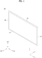
- FIG. 1 is a diagram illustrating a structure of a display unit 100 related to the present disclosure.
- the display unit 100 may be defined as one body directly including a display panel 110.
- the display unit 100 may include a first long side (LSI); a second long side (LS2), a first short side (SS1) adjacent to the LS1 and LS2; and a second short side (SS2) which is opposite to SS1.
- LSI first long side
- LS2 second long side
- SS1 first short side
- SS2 second short side
- SS1 may refer to a first side area and SS2 refer to a second side area opposite to the first side area.
- LS1 may refer to a third side area located between the first and second side areas, adjacent to them.
- LS2 may refer to a fourth side area located between the first and second side areas, opposite to the third side area.
- LS1 and LS2 are longer than SS1 and SS2. However, LS1 and LS2 may be almost equally long as SS1 and SS2.
- a first direction (DR1) may be a direction parallel with the long sides of the display unit 100 (LSI and LS2).
- a second direction (DR2) may be a direction parallel with the short sides (SS1 and SS2) of the display unit 100.
- a third direction (DR3) may be a direction perpendicular to the first direction (DR1) and/or the second direction (DR2).
- DR1 and DR2 may be collectively called the horizontal directions.
- DR3 may be called the vertical direction.
- FIG. 2 is a diagram illustrating one embodiment of a display device 10 in accordance with the present disclosure.
- the display device 10 may independently include the display unit 100 and the AV box 210.
- the display unit 100 and the AV box 210 may exchange or transceive electrical signals.
- the AV box 210 may load electronic components for driving the display device therein.
- the electronic components may include a battery functioning as a power supply unit; a main board; a wireless communication module; and a speaker.
- the physical separation of the display unit 100 and the AV box 210 may result in the display unit 100 and the AV box 210 being spaced a preset distance from each other.
- the AV box 210 may be mounted on the floor and the display unit 100 may be mounted or attached to the wall 300, so that a user can focus more on an output region of the display unit 100.
- the display unit 100 and the AV box 210 may transceive signals via wire or wirelessly.
- the wire using configuration is defined as a first cable 220. Such the connection will be described in detail later.
- the display unit 100 and the AV box 210 may tranceive signals with each other wirelessly as shown in FIG. 2(b) .
- FIG. 3 is an exploded perspective diagram illustrating the display unit 100 in accordance with the present disclosure.
- the display panel 110 is provided on a front surface of the display unit 100 and configured to display an image.
- the display panel 110 is controlled to divide the image into a plurality of pixels which emit lights with hue saturation intensity, respectively, to output the image.
- the display panel 110 may be a rectangular flat display. As one alternative example, it may be a curved display.
- the display panel 110 may have a different configuration according as whether the display device 10 is the OLED type or LCD type.
- the display panel 110 may include a metal sheet 116 provided in the rearmost side.
- the display panel provided only as it is has a low strength level enough to cause panel bending and damage and the metal sheet 116 is employed to supplement or compensate the strength.
- a source PCB 120 may be provided in a rear surface of the display. Signal wires for transmitting digital video data and timing control signals of the main board or interface board 130 may be located in the source PCB 120.
- the interface board 130 is electrically connected with the source PCB 120 and components for transmitting a signal to the source PCB 120 are loaded in the interface board 130.
- the interface board 130 may be provided as PCB (Printed Circuit Board).
- the interface board 130 has a reception interface IC loaded therein to receive a signal from a transmission interface IC provided in the AV box 220 and transmit the signal to the source PCB 120.
- the module cover 140 is provided to cover the rear surface of the display panel 110 and directly attached to the display panel 110.
- the module cover 140 may support the rear surface of the display panel 110 and define the rear exterior of the display unit 100.
- the module cover 140 may cover a rear surface of the source PCB 120.
- a PCB cover configured to expose the source PCB 120 may additionally cover the source PCB 120 to define the rear exterior of the display unit 100 (not shown).
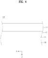
- FIG. 4 is a cross sectional diagram illustrating one region of a display panel. 110.
- the display panel 110 of the display device 10 in accordance with the present disclosure may be the OLED type display.
- the display panel 110 may include a transparent substrate 111; an upper electrode 112; an organic light emitting layer 113; and a lower electrode 114.
- the transparent substrate 111, the upper electrode 112, the organic light emitting layer 113 and the lower electrode 114 may be formed sequentially.
- the transparent substrate 11 and the upper electrode 112 may include a transparent material.
- the lower electrode 114 may include an opaque material.
- the embodiments of the present disclosure are not limited thereto and the may include a transparent material (for example, ITO and the like). In this instance, light may be emitted from one surface of the lower electrode 114.
- a light shade plate may be further formed behind the lower electrode 114.
- the OLED display device 10 configured as mentioned above may require no auxiliary light sources and is able to reduce the volume and weight of the display device 10. Also, the OLED display device 10 has a faster reaction speed than the LCD display device 10, so that it may have an advantage of no afterimage when displaying an image.
- the metal sheet 116 disposed in the rearmost surface of the display panel 110 is not technically the component which affects the image output but a part of the display panel 110 for easy description sake.
- FIG. 5 is a cross sectional diagram illustrating one region of the display unit 100.
- the display panel 110 and the module cover 140 may be attached to the display device 10 in accordance with the present disclosure by using an adhesive sheet 115.
- the adhesive sheet 115 may include a double adhesive tape having both sides which are adhesive.
- the adhesive sheet 115 may have an auxiliary thickness so that foreign substances might come into a gap between the display panel 110 and the module cover 140.
- a sealing member 1151 may side-seal at least one side of the adhesive sheet 115 as shown in FIG. 5 (a) .
- the sealing member 1151 may shield a predetermined region of the adhesive sheet 115 and a predetermined portion of the display panel 110 simultaneously.
- a frame 1152 shown in FIG. 5 (b) may be inserted in a predetermined region of the adhesive sheet 115.
- the frame 1152 may be in contact with some region of the adhesive sheet 115 and bending, with one end extended toward the display panel 110. Accordingly, the frame 1152 may shield the predetermined region of the display panel 110.
- a middle cabinet 1153 shown in FIG. 5 (c) may be disposed between the display panel 110 and the module cover 140.
- the middle cabinet 1153 is configured to guide the coupling position of the display panel 110.
- the middle cabinet 1153 may include a flange 1154 inserted between the display panel 110 and the module cover 140.
- a body of the middle cabinet 1153 may be configured to shield a predetermined region of the display panel 110 and a predetermined region of the module cover 140 simultaneously.
- the flange 1154 of the middle cabinet 1153 may be spaced a preset distance apart from the adhesive sheet 115. Accordingly, the adhesive sheet 115 need not be located in the overall region of the display panel 110 so as to reduce the amount of the adhesive sheet 115 needed when the display device 10 is manufactured.
- an edge of the module cover 140 shown in FIG. 5 (d) may bend toward the display panel 110. Since the edge of the module cover 140 is bending, a predetermined region of the adhesive sheet 115 may be shielded from the outside.
- the manufacturing process of the display device 10 can be simplified and the production cost can be lowered.
- the edge of the module cover 140 may be spaced a preset distance apart from the adhesive sheet 115 so that the adhesive sheet 115 may not be provided in the entire region of the display panel 110 to reduce the amount of the adhesive sheet 115.
- the structures located in a lateral surface of the adhesive sheet 115 are omitted when describing following embodiments for easy description sake.
- the structures located in the lateral surface of the adhesive sheet 115 may be applicable to the other following embodiments.
- FIG. 6 is a diagram illustrating a state where the source PCB 120 is connected with the display pane 110 via a second cable 121.
- the source PCB 120 is electrically connected with the display panel 120 to transmit or receive a signal.
- the second cable 121 connects the source PCB 120 with the display panel 110.
- a plurality of second cables 121 may be provided to connect plural points of the source PCB 120 with plural points of the display panel 110.
- the points located in the display panel 110 connected with the second cable 121 may be some of non-display area (N/A) in which no pixels are provided.
- the second cable 121 may be provided as a flexible cable, for example, FPC.
- the drive unit 122 may be provided on a substrate as COG (Chip On Glass) or on the second cable 121 as COF (Chip On Film)
- FIG. 7 is a sectional view illustrating the region where the source PCB 120 and the display panel 110 are connected with each other via the second cable 121.
- the source PCB 120 may be arranged on the rear surface of the display panel 110 to minimize a bezel area of the display unit 100.
- the source PCB 120 may be fixed to the display panel 110, especially, the metal sheet 116 by an adhesive material 123.
- a holder or rest structure independently provided without the adhesive material 123 so as to prevent the second cable 121 from being damaged by the movement generated between the source PCB 120 and the display panel 110.
- the end of the second cable 121 connected with the display panel 110 may be defined as one side 1211 and the other end connected with the source PCB 120 as the other side 1212.
- An area between one region1211 and the other region 1212 of the second cabinet 121 may be defined as a middle side 1213.
- the one side 1211 of the second cable 121 is connected with the display panel 110 from outside toward inside with respect to a second direction.
- the other side 1212 of the second cable 121 is also connected with the source PCB 120 from outside toward inside.
- That connection facilitates at least one area of the middle side 1213 of the second cable 121 to be wounded.
- the second cable 121 is bending in a 'U' shape to connect the display panel 110 and the source PCB 120.
- connection The characteristic of that connection is defined as forward bonding.
- the forward bonding is the connection not penetrating the other components but avoiding them, so as to result in no electrical loss. Accordingly, it is proper to use that connection in the large-inch display device 10.
- the second cable 121 provided in the U-shaped forward bonding may occupy a space of a thickness (T1) with respect to a third direction, in other words, a direction along the thickness of the display unit 100. It is necessary that the width between the rear surface of the display panel 110 and an inner surface of the module cover 140 should be secured to be as large as T1 or more, because there is great concern about damage to the second cable 121 which might be caused by an external force in a direction along the width.
- the thickness (T2) of the source PCB 120 which occupies the rear surface of the display panel 110 may be larger than the thickness (T1) of the second cable 121.
- the width between the rear surface of the display panel 110 and the inner surface of the module cover 140 has to be secured to be as large as T2 or more.
- the thickness of the display unit 100 may be influenced by the space (T1) occupied by the second cable 121 or the space (T2) occupied by the source PCB 120.
- the forward bonding may be influenced more by the space (T1) occupied by the second cable 121.
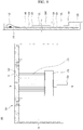
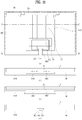
- FIG. 8 includes a rear view of the display unit 100 and a sectional diagram along A-A'.
- the rear view shows a state including no module cover 140 and the sectional view shows a state having the module cover 140.
- the source PCB 120 may be located in a lower end of the rear surface of the display panel 110.
- An interface board 130 connected with the source PCB 120 may be located in an upper area of the source PCB 120 of the rear surface of the display panel 110.
- the second cable121 may connect a lower end of the source PCB 120 and a lower end of the display panel 110 with each other, using the forward bonding mentioned above.
- the first cable 220 is configured to electrically connect the AV box 210 with the interface board 130, to transmit an electrical signal to the AV box 210, the interface board 130, a third cable 131, the source PCB 120, the second cable 121 and the display panel 110 in order or in reverse order.
- the first cable 220 connected with the interface board 130 has to come out from one side of the display unit 100 to be connected with the AV box 210.
- the AV box 220 is located under the display unit 100 so that the first cable 220 may come out from a lower end of the display unit 100.
- the first cable 220 may be exhausted from an outside, especially, an outer end of the display unit 100 via a hole 142 formed in the module cover 140.
- the first cable 220 may be exhausted from the outside, especially, the outer end of the display unit 100 via a slit 143 formed between the module cover 140 and a back cover 141 covering the hole 142 of the module cover 140.
- the second cable 121, the module cover 140 and the first cable 220 are overlapped or the source PCB 120, the module cover 140 and the first cable 220 are overlapped.
- Such the structure may end up with the increase of the thickness.
- the thickness of the display unit 100 may be increased more.
- FIG. 9 includes a rear view of the display unit 100 and a sectional diagram along B-B'.
- the source PCB 120 may be located in an upper end of the display unit 100.
- the source PCB 120 may be provided in an upper end of the rear surface of the display panel 110 and the interface board 130 may be located in the rear surface of the display panel 110, under the source PCB 120.
- the second cable 121 may be connected with the upper end of the display panel 110 and the upper end of the source PCB 120 by the forward bonding mentioned above.
- the interface board 130 is connected with the source PCB 120 via the third cable 131.
- the third cable 131 may be connected to one side of the interface 130. Especially, the side may be an upper end of the interface board 130.
- the first cable 220 may be connected with the other side of the interface board 130.
- the other side may be a lower end of the interface board 130.
- the first cable 220 connected with the other side of the interface board 130 may be drawn out from the lower end of the display unit 100 and connected with the AV box 210.
- the first cable 220 may not be overlapped with the source PCB 120 or itself in any areas.
- the width between the rear surface of the display panel 110 and the inner surface of the module cover 140 may be uniformly distributed, so as to reduce the overall thickness of the display unit 100.
- the module cover 140 may be configured to cover the rear surface of the display panel 110 as well as the area having the second cable 121 and the source PCB 120. To facilitate the connecting or disconnecting of the first cable 220 to or from the display unit 100, the module cover 140 may include an opening 142 for exposing at least predetermined area of the interface board 130 to the rear surface.
- the back cover 141 may be provided to cover the opening 142 not to expose the rear surface of the interface board 130 to the rear surface of the display unit 100. In other words, even the connection area between the first cable 220 and the interface board 130 may be covered with the back cover 141 so as to define the clean exterior.
- the first cable 220 may be drawn out from the lower end of the display unit 100 along the outside of the module cover 140 via the slit 143 formed between the module cover 140 and the back cover 141.
- the increase of the thickness enabled by the arrangement shown in FIG. 9 may be on the premise that a virtual line of the first cable having a first width will meet the second cable 121 or the source PCB 120.
- the arrangement divided along both directions of the source PCB 120 and the interface board 130 as shown in FIG. 9 may not only bring the minimized thickness but also simplify the shape of the module cover 140 and enhance the freedom of the arrangement.
- first cable 220 and the second cable 121 or the first cable 220 and the source PCB 120 are spaced a preset distance apart from each other or not overlapped with each other, so that the heat generated from the components may be dispersed to the overall area of the display unit 100 enough to enhance the heat radiation efficiency.
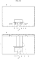
- FIG. 10 (a) is a rear view illustrating that the display unit 100 shown in FIG. 8 includes the module cover 140 and
- FIG. 10 (b) is a rear view illustrating that the display unit 100 shown in FIG. 9 includes the module cover 140.
- the hole 142 is configured to expose a first connection contact point 132 between the interface board 130 and the first cable 220.
- the hole 142 is configured to expose the third cable 131 and a second connection contact point 133 between the third cable 131 and the interface board 130 to the rear surface.
- the hole 142 is configured to expose only the first connection contact point 132 connecting the first cable 220 with the interface board 130, not the second connection contact point 133 connecting the third interface board 130 with the third cable 131. Accordingly, the exposure of the connection area between the cable and the interface which might be subject to the external force or shock can be minimized to enhance the reliability.
- the third cable 131 may be also exposed via the hole 142 as shown in FIG. 10 (a) . However, the third cable 131 is not exposed in the embodiment shown in FIG. 10 (b) so as to minimize the exposure area.
- FIG. 11 includes a rear view and a sectional view of the display unit 100.
- FIG. 11 (a) is a rear view of the display unit 100 in accordance with the present disclosure.
- the inner surface 1401 of the module cover 140 may have a recessed area 1402 formed in a corresponding portion to the components provided in the rear surface of the display panel 110.
- the corresponding components may include the source PCB 120, the second cable 121, the interface board 130 and the like.
- FIG. 11 (b) and FIG. 11(c) are sectional views along C-C' direction shown in FIG. 11 (a) .
- the module cover 140 has the recessed area 1402 formed in the inner surface 1401 so that the overall rigidity thereof could be lowered but it has an outer surface 1404 which still has a flat shape so as to prevent the display unit 100 from becoming thick in the overall area. Moreover, the lowered rigidity of the recessed area may be compensated by the rigidity of the relatively thick module cover area.
- the recessed area 1402 is formed while the overall area of the module cover 140 is uniformly thick. Accordingly, not only the inner surface 1401 but also the outer surface 1404 of the module cover 140 may have a curved shape. Such a shape may be realized by a forming, beading or pressing process, not the NC process, so as lower the production cost.
- the thickest area of the display unit 100 may equal and the other area is thinner in the embodiment shown in FIG. 11(c) enough to have versatility in the corresponding area.
- FIG. 11(d) is a sectional diagram of FIG. 11 (a) along D-D'.
- the outer surface 1404 of the module cover 140 may have a recessed area 1403 which is recessed from the rear surface forwardly, corresponding to the first cable 220.
- the recessed area 1403 seems to accommodate the first cable 220 so that the first cable 220 can be arranged in the outer surface 1404 of the module cover 140 only to minimize the increase of the thickness.
- An outer peripheral area 1405 surrounds the first cable 220 so as to minimize the possibility of damage to the first cable 220 caused by the external force. Also, the possibility of drawing the first cable 220 connected with the interface board 130 out via the lower end of the display unit 100 may be provided (see FIG. 12 ).
- FIGS. 12 and 13 are vertically-cross sectional views illustrating one embodiment of a display unit 100.
- the components provided in the rear surface of the display panel 110 are characterized in that they get thinner along a downward direction by the embodiment having the source PCV 120 provided above the rear surface of the display panel and the interface board 130 provided under the rear surface. Considering the characteristic, a different-thickness display unit 100 having the thickness between the rear surface of the module cover 140 and the front surface of the display unit 100 which gets lowered in a downward direction may be realized.
- the module cover 140 may have a step-like shape which gets more recessed downwardly.
- the module cover 140 may have a shape in which the gap between the inner surface of the module cover 140 and the rear surface 1101 of the display panel 110 becomes reduced from the upper end toward the lower end like T3, T4 and T5 sequentially.
- the outer surface 1404 of the module cover 140 may have a step-like shape of which the thickness gets more reduced downwardly.
- an inclined surface may be formed to make the display unit 100 become thinner and thinner downwardly.
- the inclined surface may have an inclination angle (G1).
- the inclination angle means the relation between the inner surface 1401 of the module cover 140 and the rear surface 1101 of the display panel 110.
- the thickness of the entire display unit 110 in other words, the front surface 1102 of the display panel and the outer surface 1404 of the module cover 140 may form the inclined surface.
- the display unit 100 When having the inclined surface, the display unit 100 may be inclinedly mounted in close contact with the wall.
- the slope of the rear surface of the module cover 140 with respect to the front surface of the display unit 100 is not so large. Even though the display unit is attached in close contact with the vertical wall 300, there is no big problem in the user's viewing.
- FIG. 14 is a rear view illustrating a further embodiment of a display unit 100.
- the embodiment of the display unit may realize the structure configured to move the interface board 130 vertically to move in or out with respect to the display unit.
- FIG. 14 (a) shows a state where the interface board 130 is moved to the lower end and FIG. 14 (b) shows a state where the interface board 130 is moved to the upper end.
- the vertically variable width of the interface board 130 becomes broad. Using that, the vertical location of the interface board 130 may be adjusted and the first cable 220 connected with the interface board 130 may be retractable with respect to the display unit 100 effectively.
- the vertical location of the interface board 130 may be adjusted to prevent the first cable 220 exposed outside the display unit 100 from getting stretched long unnecessarily.
- the interface board 130 may be movable along a rail 150 vertically.
- the rail 150 may hold both sides of the interface board 130 and the interface board 130 may be vertically sliding while being inserted in both sides of the rail 150.
- the rail 150 may include a fixing portion 151 defining an entire passage; and a moving portion 152 moving along the fixing portion 151, so that the moving portion 152 may be fixed to both sides of the interface board 130 to move the interface board 130 there along.
- the external shock or force applied to the interface board 130 may be minimized and damage to the interface board 130 may be prevented, compared with the moving structure configured to directly move the interface board 130.
- the third cable 131 may be unwounded or spread or partially overlapped along the vertical movement of the interface board 130. However, the thickness of the third cable 131 is sufficiently thin by approximately 0.1mm to secure a spare space even it is overlapped.
- FIG. 15 is a diagram illustrating the rear surface of the display unit 100 shown in FIG. 14 .
- a longitudinally expanded open area 144 may be provided in the module cover 140 to expose the connection area between the interface board 130 and the first cable 220 sufficiently.
Landscapes
- Physics & Mathematics (AREA)
- Engineering & Computer Science (AREA)
- Microelectronics & Electronic Packaging (AREA)
- Nonlinear Science (AREA)
- General Physics & Mathematics (AREA)
- Crystallography & Structural Chemistry (AREA)
- Chemical & Material Sciences (AREA)
- Optics & Photonics (AREA)
- Mathematical Physics (AREA)
- Multimedia (AREA)
- Signal Processing (AREA)
- Theoretical Computer Science (AREA)
- Devices For Indicating Variable Information By Combining Individual Elements (AREA)
Applications Claiming Priority (1)
| Application Number | Priority Date | Filing Date | Title |
|---|---|---|---|
| KR1020160168588A KR102655477B1 (ko) | 2016-12-12 | 2016-12-12 | 디스플레이 장치 |
Publications (2)
| Publication Number | Publication Date |
|---|---|
| EP3333623A1 true EP3333623A1 (de) | 2018-06-13 |
| EP3333623B1 EP3333623B1 (de) | 2021-04-21 |
Family
ID=60654708
Family Applications (1)
| Application Number | Title | Priority Date | Filing Date |
|---|---|---|---|
| EP17205754.9A Active EP3333623B1 (de) | 2016-12-12 | 2017-12-06 | Anzeigevorrichtung |
Country Status (4)
| Country | Link |
|---|---|
| US (1) | US10595426B2 (de) |
| EP (1) | EP3333623B1 (de) |
| KR (1) | KR102655477B1 (de) |
| CN (1) | CN108230941B (de) |
Cited By (1)
| Publication number | Priority date | Publication date | Assignee | Title |
|---|---|---|---|---|
| EP3764414A4 (de) * | 2018-07-12 | 2021-12-29 | LG Electronics, Inc. | Anzeigevorrichtung |
Families Citing this family (6)
| Publication number | Priority date | Publication date | Assignee | Title |
|---|---|---|---|---|
| CN110011686B (zh) * | 2018-01-03 | 2022-02-22 | 富顶精密组件(深圳)有限公司 | 无线通信互连系统及其壁挂式套件 |
| KR102654718B1 (ko) * | 2018-07-31 | 2024-04-08 | 삼성디스플레이 주식회사 | 커넥터 및 이를 포함하는 디스플레이 장치 |
| WO2020241942A1 (ko) | 2019-05-31 | 2020-12-03 | 엘지전자 주식회사 | 디스플레이 장치 |
| CN110796957B (zh) * | 2019-11-26 | 2022-01-04 | 武汉华星光电半导体显示技术有限公司 | 一种柔性显示面板及显示装置 |
| KR102293476B1 (ko) * | 2020-05-26 | 2021-08-26 | 엘지전자 주식회사 | 디스플레이 장치 |
| WO2022045405A1 (ko) * | 2020-08-28 | 2022-03-03 | 엘지전자 주식회사 | 디스플레이 디바이스 |
Citations (5)
| Publication number | Priority date | Publication date | Assignee | Title |
|---|---|---|---|---|
| US6307530B1 (en) * | 1997-07-01 | 2001-10-23 | Samsung Electronics Co., Ltd. | LCD monitor having partitioned circuit section |
| EP1455377A2 (de) * | 2003-03-05 | 2004-09-08 | Pioneer Corporation | Anzeigevorrichtung für Flachplattentyp |
| US20100302494A1 (en) * | 2009-05-29 | 2010-12-02 | Ju-Young Lee | Liquid crystal display device |
| EP2343958A2 (de) * | 2010-01-07 | 2011-07-13 | Samsung Electronics Co., Ltd. | Anzeigevorrichtung |
| KR20130077090A (ko) * | 2011-12-29 | 2013-07-09 | 삼성전자주식회사 | 디스플레이 장치 |
Family Cites Families (4)
| Publication number | Priority date | Publication date | Assignee | Title |
|---|---|---|---|---|
| KR20110055337A (ko) * | 2009-11-18 | 2011-05-25 | 삼성전자주식회사 | 디스플레이장치 |
| CA2826014C (en) * | 2011-02-17 | 2016-01-12 | Millson Custom Solutions Inc. | Mounting apparatus for an audio/video system and related methods and systems |
| US20130135528A1 (en) * | 2011-11-29 | 2013-05-30 | Funai Electric Co., Ltd. | Broadcasting Receiver and Television Set |
| JP6282832B2 (ja) * | 2013-10-01 | 2018-02-21 | 株式会社ジャパンディスプレイ | 有機el表示装置 |
-
2016
- 2016-12-12 KR KR1020160168588A patent/KR102655477B1/ko active Active
-
2017
- 2017-11-17 US US15/816,836 patent/US10595426B2/en active Active
- 2017-12-06 EP EP17205754.9A patent/EP3333623B1/de active Active
- 2017-12-12 CN CN201711317264.XA patent/CN108230941B/zh active Active
Patent Citations (5)
| Publication number | Priority date | Publication date | Assignee | Title |
|---|---|---|---|---|
| US6307530B1 (en) * | 1997-07-01 | 2001-10-23 | Samsung Electronics Co., Ltd. | LCD monitor having partitioned circuit section |
| EP1455377A2 (de) * | 2003-03-05 | 2004-09-08 | Pioneer Corporation | Anzeigevorrichtung für Flachplattentyp |
| US20100302494A1 (en) * | 2009-05-29 | 2010-12-02 | Ju-Young Lee | Liquid crystal display device |
| EP2343958A2 (de) * | 2010-01-07 | 2011-07-13 | Samsung Electronics Co., Ltd. | Anzeigevorrichtung |
| KR20130077090A (ko) * | 2011-12-29 | 2013-07-09 | 삼성전자주식회사 | 디스플레이 장치 |
Cited By (2)
| Publication number | Priority date | Publication date | Assignee | Title |
|---|---|---|---|---|
| EP3764414A4 (de) * | 2018-07-12 | 2021-12-29 | LG Electronics, Inc. | Anzeigevorrichtung |
| US11653456B2 (en) | 2018-07-12 | 2023-05-16 | Lg Electronics Inc. | Display device |
Also Published As
| Publication number | Publication date |
|---|---|
| CN108230941B (zh) | 2020-12-29 |
| US10595426B2 (en) | 2020-03-17 |
| KR20180067143A (ko) | 2018-06-20 |
| EP3333623B1 (de) | 2021-04-21 |
| US20180168060A1 (en) | 2018-06-14 |
| KR102655477B1 (ko) | 2024-04-08 |
| CN108230941A (zh) | 2018-06-29 |
Similar Documents
| Publication | Publication Date | Title |
|---|---|---|
| EP3333623B1 (de) | Anzeigevorrichtung | |
| CN106920478B (zh) | 显示设备 | |
| ES2733314T3 (es) | Dispositivo de visualización | |
| EP3177035B1 (de) | Lautsprechermodul, elektronische vorrichtung mit dem lautsprechermodul und anzeigevorrichtung mit der elektronischen vorrichtung | |
| US20160186944A1 (en) | Display Device | |
| US9195084B2 (en) | Display device and television | |
| CN107657933B (zh) | 显示装置 | |
| US9888595B2 (en) | Display device | |
| KR20190004514A (ko) | 디스플레이 디바이스 | |
| KR20150131453A (ko) | 표시장치 | |
| KR102515715B1 (ko) | 디스플레이 장치 | |
| KR20190090633A (ko) | 디스플레이 디바이스 | |
| US11770951B2 (en) | Display device | |
| US9877402B2 (en) | Display device | |
| CN111164966B (zh) | 显示装置 | |
| KR20210051076A (ko) | 디스플레이 장치 | |
| KR102492451B1 (ko) | 디스플레이 장치 | |
| KR102665993B1 (ko) | 디스플레이 디바이스 | |
| US10194539B2 (en) | Display device | |
| US20260018144A1 (en) | Display device | |
| KR102091113B1 (ko) | 슬림형 대화면 시현기 | |
| US10852575B2 (en) | Display apparatus having front cover with infrared sensor | |
| KR101354599B1 (ko) | 액정표시장치 | |
| KR20170055706A (ko) | 디스플레이 장치 | |
| KR20170006011A (ko) | 디스플레이 장치 |
Legal Events
| Date | Code | Title | Description |
|---|---|---|---|
| PUAI | Public reference made under article 153(3) epc to a published international application that has entered the european phase |
Free format text: ORIGINAL CODE: 0009012 |
|
| STAA | Information on the status of an ep patent application or granted ep patent |
Free format text: STATUS: REQUEST FOR EXAMINATION WAS MADE |
|
| 17P | Request for examination filed |
Effective date: 20171206 |
|
| AK | Designated contracting states |
Kind code of ref document: A1 Designated state(s): AL AT BE BG CH CY CZ DE DK EE ES FI FR GB GR HR HU IE IS IT LI LT LU LV MC MK MT NL NO PL PT RO RS SE SI SK SM TR |
|
| AX | Request for extension of the european patent |
Extension state: BA ME |
|
| STAA | Information on the status of an ep patent application or granted ep patent |
Free format text: STATUS: EXAMINATION IS IN PROGRESS |
|
| 17Q | First examination report despatched |
Effective date: 20190919 |
|
| GRAP | Despatch of communication of intention to grant a patent |
Free format text: ORIGINAL CODE: EPIDOSNIGR1 |
|
| STAA | Information on the status of an ep patent application or granted ep patent |
Free format text: STATUS: GRANT OF PATENT IS INTENDED |
|
| INTG | Intention to grant announced |
Effective date: 20201202 |
|
| GRAS | Grant fee paid |
Free format text: ORIGINAL CODE: EPIDOSNIGR3 |
|
| GRAA | (expected) grant |
Free format text: ORIGINAL CODE: 0009210 |
|
| STAA | Information on the status of an ep patent application or granted ep patent |
Free format text: STATUS: THE PATENT HAS BEEN GRANTED |
|
| AK | Designated contracting states |
Kind code of ref document: B1 Designated state(s): AL AT BE BG CH CY CZ DE DK EE ES FI FR GB GR HR HU IE IS IT LI LT LU LV MC MK MT NL NO PL PT RO RS SE SI SK SM TR |
|
| REG | Reference to a national code |
Ref country code: GB Ref legal event code: FG4D |
|
| REG | Reference to a national code |
Ref country code: CH Ref legal event code: EP |
|
| REG | Reference to a national code |
Ref country code: DE Ref legal event code: R096 Ref document number: 602017037014 Country of ref document: DE Ref country code: IE Ref legal event code: FG4D |
|
| REG | Reference to a national code |
Ref country code: AT Ref legal event code: REF Ref document number: 1385259 Country of ref document: AT Kind code of ref document: T Effective date: 20210515 |
|
| REG | Reference to a national code |
Ref country code: LT Ref legal event code: MG9D |
|
| REG | Reference to a national code |
Ref country code: AT Ref legal event code: MK05 Ref document number: 1385259 Country of ref document: AT Kind code of ref document: T Effective date: 20210421 |
|
| REG | Reference to a national code |
Ref country code: NL Ref legal event code: MP Effective date: 20210421 |
|
| PG25 | Lapsed in a contracting state [announced via postgrant information from national office to epo] |
Ref country code: LT Free format text: LAPSE BECAUSE OF FAILURE TO SUBMIT A TRANSLATION OF THE DESCRIPTION OR TO PAY THE FEE WITHIN THE PRESCRIBED TIME-LIMIT Effective date: 20210421 Ref country code: FI Free format text: LAPSE BECAUSE OF FAILURE TO SUBMIT A TRANSLATION OF THE DESCRIPTION OR TO PAY THE FEE WITHIN THE PRESCRIBED TIME-LIMIT Effective date: 20210421 Ref country code: HR Free format text: LAPSE BECAUSE OF FAILURE TO SUBMIT A TRANSLATION OF THE DESCRIPTION OR TO PAY THE FEE WITHIN THE PRESCRIBED TIME-LIMIT Effective date: 20210421 Ref country code: AT Free format text: LAPSE BECAUSE OF FAILURE TO SUBMIT A TRANSLATION OF THE DESCRIPTION OR TO PAY THE FEE WITHIN THE PRESCRIBED TIME-LIMIT Effective date: 20210421 Ref country code: BG Free format text: LAPSE BECAUSE OF FAILURE TO SUBMIT A TRANSLATION OF THE DESCRIPTION OR TO PAY THE FEE WITHIN THE PRESCRIBED TIME-LIMIT Effective date: 20210721 Ref country code: NL Free format text: LAPSE BECAUSE OF FAILURE TO SUBMIT A TRANSLATION OF THE DESCRIPTION OR TO PAY THE FEE WITHIN THE PRESCRIBED TIME-LIMIT Effective date: 20210421 |
|
| PG25 | Lapsed in a contracting state [announced via postgrant information from national office to epo] |
Ref country code: RS Free format text: LAPSE BECAUSE OF FAILURE TO SUBMIT A TRANSLATION OF THE DESCRIPTION OR TO PAY THE FEE WITHIN THE PRESCRIBED TIME-LIMIT Effective date: 20210421 Ref country code: SE Free format text: LAPSE BECAUSE OF FAILURE TO SUBMIT A TRANSLATION OF THE DESCRIPTION OR TO PAY THE FEE WITHIN THE PRESCRIBED TIME-LIMIT Effective date: 20210421 Ref country code: PT Free format text: LAPSE BECAUSE OF FAILURE TO SUBMIT A TRANSLATION OF THE DESCRIPTION OR TO PAY THE FEE WITHIN THE PRESCRIBED TIME-LIMIT Effective date: 20210823 Ref country code: NO Free format text: LAPSE BECAUSE OF FAILURE TO SUBMIT A TRANSLATION OF THE DESCRIPTION OR TO PAY THE FEE WITHIN THE PRESCRIBED TIME-LIMIT Effective date: 20210721 Ref country code: PL Free format text: LAPSE BECAUSE OF FAILURE TO SUBMIT A TRANSLATION OF THE DESCRIPTION OR TO PAY THE FEE WITHIN THE PRESCRIBED TIME-LIMIT Effective date: 20210421 Ref country code: LV Free format text: LAPSE BECAUSE OF FAILURE TO SUBMIT A TRANSLATION OF THE DESCRIPTION OR TO PAY THE FEE WITHIN THE PRESCRIBED TIME-LIMIT Effective date: 20210421 Ref country code: GR Free format text: LAPSE BECAUSE OF FAILURE TO SUBMIT A TRANSLATION OF THE DESCRIPTION OR TO PAY THE FEE WITHIN THE PRESCRIBED TIME-LIMIT Effective date: 20210722 Ref country code: IS Free format text: LAPSE BECAUSE OF FAILURE TO SUBMIT A TRANSLATION OF THE DESCRIPTION OR TO PAY THE FEE WITHIN THE PRESCRIBED TIME-LIMIT Effective date: 20210821 |
|
| REG | Reference to a national code |
Ref country code: DE Ref legal event code: R097 Ref document number: 602017037014 Country of ref document: DE |
|
| PG25 | Lapsed in a contracting state [announced via postgrant information from national office to epo] |
Ref country code: RO Free format text: LAPSE BECAUSE OF FAILURE TO SUBMIT A TRANSLATION OF THE DESCRIPTION OR TO PAY THE FEE WITHIN THE PRESCRIBED TIME-LIMIT Effective date: 20210421 Ref country code: ES Free format text: LAPSE BECAUSE OF FAILURE TO SUBMIT A TRANSLATION OF THE DESCRIPTION OR TO PAY THE FEE WITHIN THE PRESCRIBED TIME-LIMIT Effective date: 20210421 Ref country code: DK Free format text: LAPSE BECAUSE OF FAILURE TO SUBMIT A TRANSLATION OF THE DESCRIPTION OR TO PAY THE FEE WITHIN THE PRESCRIBED TIME-LIMIT Effective date: 20210421 Ref country code: EE Free format text: LAPSE BECAUSE OF FAILURE TO SUBMIT A TRANSLATION OF THE DESCRIPTION OR TO PAY THE FEE WITHIN THE PRESCRIBED TIME-LIMIT Effective date: 20210421 Ref country code: CZ Free format text: LAPSE BECAUSE OF FAILURE TO SUBMIT A TRANSLATION OF THE DESCRIPTION OR TO PAY THE FEE WITHIN THE PRESCRIBED TIME-LIMIT Effective date: 20210421 Ref country code: SK Free format text: LAPSE BECAUSE OF FAILURE TO SUBMIT A TRANSLATION OF THE DESCRIPTION OR TO PAY THE FEE WITHIN THE PRESCRIBED TIME-LIMIT Effective date: 20210421 Ref country code: SM Free format text: LAPSE BECAUSE OF FAILURE TO SUBMIT A TRANSLATION OF THE DESCRIPTION OR TO PAY THE FEE WITHIN THE PRESCRIBED TIME-LIMIT Effective date: 20210421 |
|
| PLBE | No opposition filed within time limit |
Free format text: ORIGINAL CODE: 0009261 |
|
| STAA | Information on the status of an ep patent application or granted ep patent |
Free format text: STATUS: NO OPPOSITION FILED WITHIN TIME LIMIT |
|
| 26N | No opposition filed |
Effective date: 20220124 |
|
| PG25 | Lapsed in a contracting state [announced via postgrant information from national office to epo] |
Ref country code: IS Free format text: LAPSE BECAUSE OF FAILURE TO SUBMIT A TRANSLATION OF THE DESCRIPTION OR TO PAY THE FEE WITHIN THE PRESCRIBED TIME-LIMIT Effective date: 20210821 Ref country code: AL Free format text: LAPSE BECAUSE OF FAILURE TO SUBMIT A TRANSLATION OF THE DESCRIPTION OR TO PAY THE FEE WITHIN THE PRESCRIBED TIME-LIMIT Effective date: 20210421 |
|
| PG25 | Lapsed in a contracting state [announced via postgrant information from national office to epo] |
Ref country code: MC Free format text: LAPSE BECAUSE OF FAILURE TO SUBMIT A TRANSLATION OF THE DESCRIPTION OR TO PAY THE FEE WITHIN THE PRESCRIBED TIME-LIMIT Effective date: 20210421 Ref country code: IT Free format text: LAPSE BECAUSE OF FAILURE TO SUBMIT A TRANSLATION OF THE DESCRIPTION OR TO PAY THE FEE WITHIN THE PRESCRIBED TIME-LIMIT Effective date: 20210421 |
|
| REG | Reference to a national code |
Ref country code: CH Ref legal event code: PL |
|
| REG | Reference to a national code |
Ref country code: BE Ref legal event code: MM Effective date: 20211231 |
|
| PG25 | Lapsed in a contracting state [announced via postgrant information from national office to epo] |
Ref country code: LU Free format text: LAPSE BECAUSE OF NON-PAYMENT OF DUE FEES Effective date: 20211206 Ref country code: IE Free format text: LAPSE BECAUSE OF NON-PAYMENT OF DUE FEES Effective date: 20211206 |
|
| PG25 | Lapsed in a contracting state [announced via postgrant information from national office to epo] |
Ref country code: BE Free format text: LAPSE BECAUSE OF NON-PAYMENT OF DUE FEES Effective date: 20211231 |
|
| PG25 | Lapsed in a contracting state [announced via postgrant information from national office to epo] |
Ref country code: LI Free format text: LAPSE BECAUSE OF NON-PAYMENT OF DUE FEES Effective date: 20211231 Ref country code: CH Free format text: LAPSE BECAUSE OF NON-PAYMENT OF DUE FEES Effective date: 20211231 |
|
| PG25 | Lapsed in a contracting state [announced via postgrant information from national office to epo] |
Ref country code: HU Free format text: LAPSE BECAUSE OF FAILURE TO SUBMIT A TRANSLATION OF THE DESCRIPTION OR TO PAY THE FEE WITHIN THE PRESCRIBED TIME-LIMIT; INVALID AB INITIO Effective date: 20171206 |
|
| PG25 | Lapsed in a contracting state [announced via postgrant information from national office to epo] |
Ref country code: CY Free format text: LAPSE BECAUSE OF FAILURE TO SUBMIT A TRANSLATION OF THE DESCRIPTION OR TO PAY THE FEE WITHIN THE PRESCRIBED TIME-LIMIT Effective date: 20210421 |
|
| PG25 | Lapsed in a contracting state [announced via postgrant information from national office to epo] |
Ref country code: MK Free format text: LAPSE BECAUSE OF FAILURE TO SUBMIT A TRANSLATION OF THE DESCRIPTION OR TO PAY THE FEE WITHIN THE PRESCRIBED TIME-LIMIT Effective date: 20210421 |
|
| PG25 | Lapsed in a contracting state [announced via postgrant information from national office to epo] |
Ref country code: MT Free format text: LAPSE BECAUSE OF FAILURE TO SUBMIT A TRANSLATION OF THE DESCRIPTION OR TO PAY THE FEE WITHIN THE PRESCRIBED TIME-LIMIT Effective date: 20210421 |
|
| PG25 | Lapsed in a contracting state [announced via postgrant information from national office to epo] |
Ref country code: TR Free format text: LAPSE BECAUSE OF FAILURE TO SUBMIT A TRANSLATION OF THE DESCRIPTION OR TO PAY THE FEE WITHIN THE PRESCRIBED TIME-LIMIT Effective date: 20210421 |
|
| PGFP | Annual fee paid to national office [announced via postgrant information from national office to epo] |
Ref country code: DE Payment date: 20251105 Year of fee payment: 9 |
|
| PGFP | Annual fee paid to national office [announced via postgrant information from national office to epo] |
Ref country code: GB Payment date: 20251105 Year of fee payment: 9 |
|
| PGFP | Annual fee paid to national office [announced via postgrant information from national office to epo] |
Ref country code: FR Payment date: 20251111 Year of fee payment: 9 |