EP3330848A2 - Erkennung von stapelspeicherüberlauf in einem multithread-prozessor - Google Patents
Erkennung von stapelspeicherüberlauf in einem multithread-prozessor Download PDFInfo
- Publication number
- EP3330848A2 EP3330848A2 EP17183239.7A EP17183239A EP3330848A2 EP 3330848 A2 EP3330848 A2 EP 3330848A2 EP 17183239 A EP17183239 A EP 17183239A EP 3330848 A2 EP3330848 A2 EP 3330848A2
- Authority
- EP
- European Patent Office
- Prior art keywords
- stack
- memory
- limit
- multithreaded processor
- region
- Prior art date
- Legal status (The legal status is an assumption and is not a legal conclusion. Google has not performed a legal analysis and makes no representation as to the accuracy of the status listed.)
- Granted
Links
Images




Classifications
-
- G—PHYSICS
- G06—COMPUTING OR CALCULATING; COUNTING
- G06F—ELECTRIC DIGITAL DATA PROCESSING
- G06F9/00—Arrangements for program control, e.g. control units
- G06F9/06—Arrangements for program control, e.g. control units using stored programs, i.e. using an internal store of processing equipment to receive or retain programs
- G06F9/30—Arrangements for executing machine instructions, e.g. instruction decode
- G06F9/38—Concurrent instruction execution, e.g. pipeline or look ahead
- G06F9/3861—Recovery, e.g. branch miss-prediction, exception handling
- G06F9/3865—Recovery, e.g. branch miss-prediction, exception handling using deferred exception handling, e.g. exception flags
-
- G—PHYSICS
- G06—COMPUTING OR CALCULATING; COUNTING
- G06F—ELECTRIC DIGITAL DATA PROCESSING
- G06F9/00—Arrangements for program control, e.g. control units
- G06F9/06—Arrangements for program control, e.g. control units using stored programs, i.e. using an internal store of processing equipment to receive or retain programs
- G06F9/30—Arrangements for executing machine instructions, e.g. instruction decode
- G06F9/30003—Arrangements for executing specific machine instructions
- G06F9/3005—Arrangements for executing specific machine instructions to perform operations for flow control
- G06F9/30054—Unconditional branch instructions
-
- G—PHYSICS
- G06—COMPUTING OR CALCULATING; COUNTING
- G06F—ELECTRIC DIGITAL DATA PROCESSING
- G06F9/00—Arrangements for program control, e.g. control units
- G06F9/06—Arrangements for program control, e.g. control units using stored programs, i.e. using an internal store of processing equipment to receive or retain programs
- G06F9/30—Arrangements for executing machine instructions, e.g. instruction decode
- G06F9/30098—Register arrangements
- G06F9/30101—Special purpose registers
-
- G—PHYSICS
- G06—COMPUTING OR CALCULATING; COUNTING
- G06F—ELECTRIC DIGITAL DATA PROCESSING
- G06F9/00—Arrangements for program control, e.g. control units
- G06F9/06—Arrangements for program control, e.g. control units using stored programs, i.e. using an internal store of processing equipment to receive or retain programs
- G06F9/30—Arrangements for executing machine instructions, e.g. instruction decode
- G06F9/30098—Register arrangements
- G06F9/3012—Organisation of register space, e.g. banked or distributed register file
- G06F9/30123—Organisation of register space, e.g. banked or distributed register file according to context, e.g. thread buffers
-
- G—PHYSICS
- G06—COMPUTING OR CALCULATING; COUNTING
- G06F—ELECTRIC DIGITAL DATA PROCESSING
- G06F9/00—Arrangements for program control, e.g. control units
- G06F9/06—Arrangements for program control, e.g. control units using stored programs, i.e. using an internal store of processing equipment to receive or retain programs
- G06F9/30—Arrangements for executing machine instructions, e.g. instruction decode
- G06F9/30098—Register arrangements
- G06F9/3012—Organisation of register space, e.g. banked or distributed register file
- G06F9/30134—Register stacks; shift registers
-
- G—PHYSICS
- G06—COMPUTING OR CALCULATING; COUNTING
- G06F—ELECTRIC DIGITAL DATA PROCESSING
- G06F9/00—Arrangements for program control, e.g. control units
- G06F9/06—Arrangements for program control, e.g. control units using stored programs, i.e. using an internal store of processing equipment to receive or retain programs
- G06F9/30—Arrangements for executing machine instructions, e.g. instruction decode
- G06F9/30145—Instruction analysis, e.g. decoding, instruction word fields
- G06F9/3016—Decoding the operand specifier, e.g. specifier format
-
- G—PHYSICS
- G06—COMPUTING OR CALCULATING; COUNTING
- G06F—ELECTRIC DIGITAL DATA PROCESSING
- G06F9/00—Arrangements for program control, e.g. control units
- G06F9/06—Arrangements for program control, e.g. control units using stored programs, i.e. using an internal store of processing equipment to receive or retain programs
- G06F9/30—Arrangements for executing machine instructions, e.g. instruction decode
- G06F9/32—Address formation of the next instruction, e.g. by incrementing the instruction counter
- G06F9/322—Address formation of the next instruction, e.g. by incrementing the instruction counter for non-sequential address
- G06F9/323—Address formation of the next instruction, e.g. by incrementing the instruction counter for non-sequential address for indirect branch instructions
-
- G—PHYSICS
- G06—COMPUTING OR CALCULATING; COUNTING
- G06F—ELECTRIC DIGITAL DATA PROCESSING
- G06F9/00—Arrangements for program control, e.g. control units
- G06F9/06—Arrangements for program control, e.g. control units using stored programs, i.e. using an internal store of processing equipment to receive or retain programs
- G06F9/30—Arrangements for executing machine instructions, e.g. instruction decode
- G06F9/38—Concurrent instruction execution, e.g. pipeline or look ahead
- G06F9/3836—Instruction issuing, e.g. dynamic instruction scheduling or out of order instruction execution
- G06F9/3851—Instruction issuing, e.g. dynamic instruction scheduling or out of order instruction execution from multiple instruction streams, e.g. multistreaming
-
- G—PHYSICS
- G06—COMPUTING OR CALCULATING; COUNTING
- G06F—ELECTRIC DIGITAL DATA PROCESSING
- G06F9/00—Arrangements for program control, e.g. control units
- G06F9/06—Arrangements for program control, e.g. control units using stored programs, i.e. using an internal store of processing equipment to receive or retain programs
- G06F9/30—Arrangements for executing machine instructions, e.g. instruction decode
- G06F9/38—Concurrent instruction execution, e.g. pipeline or look ahead
- G06F9/3861—Recovery, e.g. branch miss-prediction, exception handling
-
- G—PHYSICS
- G06—COMPUTING OR CALCULATING; COUNTING
- G06F—ELECTRIC DIGITAL DATA PROCESSING
- G06F9/00—Arrangements for program control, e.g. control units
- G06F9/06—Arrangements for program control, e.g. control units using stored programs, i.e. using an internal store of processing equipment to receive or retain programs
- G06F9/46—Multiprogramming arrangements
- G06F9/50—Allocation of resources, e.g. of the central processing unit [CPU]
- G06F9/5005—Allocation of resources, e.g. of the central processing unit [CPU] to service a request
- G06F9/5011—Allocation of resources, e.g. of the central processing unit [CPU] to service a request the resources being hardware resources other than CPUs, Servers and Terminals
- G06F9/5016—Allocation of resources, e.g. of the central processing unit [CPU] to service a request the resources being hardware resources other than CPUs, Servers and Terminals the resource being the memory
-
- G—PHYSICS
- G06—COMPUTING OR CALCULATING; COUNTING
- G06F—ELECTRIC DIGITAL DATA PROCESSING
- G06F12/00—Accessing, addressing or allocating within memory systems or architectures
- G06F12/02—Addressing or allocation; Relocation
- G06F12/08—Addressing or allocation; Relocation in hierarchically structured memory systems, e.g. virtual memory systems
- G06F12/10—Address translation
- G06F12/1027—Address translation using associative or pseudo-associative address translation means, e.g. translation look-aside buffer [TLB]
-
- G—PHYSICS
- G06—COMPUTING OR CALCULATING; COUNTING
- G06F—ELECTRIC DIGITAL DATA PROCESSING
- G06F12/00—Accessing, addressing or allocating within memory systems or architectures
- G06F12/14—Protection against unauthorised use of memory or access to memory
- G06F12/1416—Protection against unauthorised use of memory or access to memory by checking the object accessibility, e.g. type of access defined by the memory independently of subject rights
- G06F12/1425—Protection against unauthorised use of memory or access to memory by checking the object accessibility, e.g. type of access defined by the memory independently of subject rights the protection being physical, e.g. cell, word, block
- G06F12/1441—Protection against unauthorised use of memory or access to memory by checking the object accessibility, e.g. type of access defined by the memory independently of subject rights the protection being physical, e.g. cell, word, block for a range
-
- G—PHYSICS
- G06—COMPUTING OR CALCULATING; COUNTING
- G06F—ELECTRIC DIGITAL DATA PROCESSING
- G06F2212/00—Indexing scheme relating to accessing, addressing or allocation within memory systems or architectures
- G06F2212/68—Details of translation look-aside buffer [TLB]
- G06F2212/681—Multi-level TLB, e.g. microTLB and main TLB
Definitions
- Embodiments presented in this disclosure generally relate to computer architecture, and more specifically, techniques for reducing the amount of stack usage in a multithreaded processor.
- Multithreaded processors support execution of many processes occurring in parallel, such as using thread-level or process-level parallelism.
- a multithreaded network processor may permit thousands of threads to simultaneously operate to process network traffic packets.
- a stack region is allocated in memory for each thread.
- allocating memory for a large number of threads supported by a multithreaded processor can require a relatively large amount of memory, which occupies a significant amount of space on an integrated circuit (IC) comprising the multithreaded processor, and in some cases limits other functionality that may be implemented in the IC.
- IC integrated circuit
- the multithreaded processor comprises a first control register configured to store a stack limit value, and instruction decode logic configured to, upon receiving a procedure entry instruction for a stack associated with a first thread, determine whether to throw a stack limit exception based on the stack limit value and a first predefined stack region size associated with the stack.
- Another embodiment presented in this disclosure is a method performed by a multithreaded processor executing a plurality of threads.
- the method comprises receiving a procedure entry instruction at instruction decode logic of the multithreaded processor, the procedure entry instruction corresponding to a first thread of the plurality of threads and a stack associated therewith.
- the method further comprises accessing a first control register of the multithreaded processor to retrieve a stack limit value, and determining whether to throw a stack limit exception based on the stack limit value and a first predefined frame size associated with the procedure entry instruction.
- the memory comprises a plurality of first memory pages, each first memory page comprising a first plurality of memory regions each having a first predefined stack region size, a first stack assigned to a first memory region of the first plurality of memory regions, the first stack corresponding to a first thread of the plurality of threads.
- the memory further comprises a plurality of second memory pages, each second memory page comprising a second plurality of memory regions each having a second predefined stack region size greater than the first predefined stack region size.
- the multithreaded processor is configured to throw a stack limit exception upon determining that a size of the first stack will exceed the first predefined stack region size, and reassign, upon throwing the stack limit exception, the first stack to a second memory region of the second plurality of memory regions.
- Embodiments are generally directed to a multithreaded processor for executing a plurality of threads.
- the multithreaded processor comprises a first control register configured to store a stack limit value and instruction decode logic configured to, upon receiving a procedure entry instruction for a stack associated with a first thread, determine whether to throw a stack limit exception based on the stack limit value and a first predefined stack region size associated with the stack.
- the multithreaded processor further comprises a second control register configured to store a plurality of stack limit enable bits, where each stack limit enable bit of the plurality of stack limit enable bits corresponds to a respective thread of the plurality of threads.
- the instruction decode logic is further configured to determine, upon receiving the procedure entry instruction and based on a first stack limit enable bit of the plurality of stack limit enable bits that is associated with the first thread, whether to determine whether to throw the stack limit exception.
- Including specialized control registers for storing a stack limit value and/or a plurality of stack limit enable bits generally allow each thread's stack to be allocated a tailored amount of memory, which reduces the overall amount of memory needed to support the plurality of threads while still supporting acceptable processing performance for general cases.
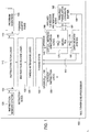
- FIG. 1 is a block diagram of an exemplary multithreaded embedded processor, according to one or more embodiments disclosed herein.
- a multithreaded processor 100 may be used in conjunction with a pipelined translation look-aside buffer (TLB) 185.
- TLB pipelined translation look-aside buffer
- the pipelined TLB 185 described below can generally be used in any computer system or computer architecture that uses address translation.
- the pipelined buffering scheme described below can be used with personal computers (PCs), supercomputers, personal digital assistants (PDAs), digital signal processors (DSPs), packet processing systems, etc.
- the multithreaded processor 100 comprises a network processor configured to process and route data packets.
- the following description is included to illustrate the operation of preferred embodiments rather than to limit the scope of the disclosure.
- Multiple program counters 105 store values in instruction memory 125 corresponding to the next instructions to be fetched for associated threads supported by the multithreaded processor 100.
- Program counter buses 110 convey the values from the program counters 105 to instruction fetch logic 115 and convey updates from instruction fetch logic 115 to the program counters 105.
- the instruction fetch logic 115 generally sequences instruction fetches from an instruction memory system 125, detects exceptions related to instruction fetching, and identifies instruction boundaries.
- Instruction buses 120 convey instruction addresses from the instruction fetch logic 115 to the instruction memory system 125, and convey results from the instruction memory system 125 back to the instruction fetch logic 115.
- the instruction memory system 125 looks up instructions using a static random access memory (SRAM) or caches, and returns the instructions to the instruction fetch logic 115.
- SRAM static random access memory
- the instruction fetch logic 115 sends raw instruction bytes to instruction decode logic 130 for mapping the raw instruction bytes into control signals to operate the multithreaded embedded multithreaded processor 100.
- Thread interleave logic 135 examines the control signals from the instruction decode logic 130 and past history to determine which thread should execute the next instruction.
- thread state 140 Based on the result(s) of the thread interleave logic 135, thread state 140 produces operands 145 for integer instruction logic 155 and for virtual address generation logic 160. Results from the integer instruction logic 155 and data memory system 190 are used to update the thread state 140 via result buses 150. Integer instruction logic 155 uses operands 145 and signals from the instruction decode logic 130 to evaluate integer operations such as addition, subtraction, shifting and masking.
- Virtual address generation logic 160 uses operands 145 to compute a virtual address (VA) 165 using, e.g., shifting and addition.
- VA virtual address
- the virtual address 165 is passed to a micro TLB 170.
- the micro TLB 170 converts the virtual address 165 into a physical address (PA) 175.
- PA physical address
- the micro TLB 170 contains a small cache of virtual address to physical address translations to support low latency lookups, but generally may suffer a higher miss rate than a larger TLB.
- the micro TLB 170 posts miss requests over pipelined TLB request and response buses 180 to the pipelined TLB 185.
- Results from the pipelined TLB 185 are transmitted back to the micro TLB 170 over the pipelined TLB request and response buses 180.
- Data memory 190 acts on the address from bus PA 175 and operands 145 to perform memory load and store operations.
- the results from data memory 190 are returned to the thread state 140 over result buses 150 and may include addresses, data, or any other information needed by the integer instruction logic 155 for conducting logic operations.
- the data memory system 190 may also contain packet data.
- the integer instruction logic 155 can also be used to read and write entries in the pipelined TLB 185 via buses 195.
- the multithreaded processor 100 may need to access a larger physical memory space (corresponding to PA 175) than what is provided by the internal virtual address space (corresponding to VA 165). Accordingly, the TLBs 170 and 185 provide virtual to physical address translations that effectively increase the size of physical address space accessible by the multiple threads of multithreaded processor 100.
- Pipelined TLB 185 holds a relatively large number of address translations and is permitted to perform translations with a higher latency than the micro TLB 170. Even though the content-addressable memories (CAMs) used in the pipelined TLB 185 can be relatively slow, the pipelined TLB 185 can still provide one address translation per clock cycle to avoid stalling of unrelated threads.
- CAMs content-addressable memories
- the pipelined TLB 185 provides a fully associative memory mapping with the power advantages of set-associative memory mapping.
- the pipelining structure in TLB 185 is also well-adapted to the multithreaded processor 100 described in FIG. 1 where multiple memory lookups may be evaluated in parallel.
- FIG. 2 is a block diagram illustrating an exemplary arrangement of control registers used for allocating stack regions for threads, according to one or more embodiments disclosed herein.
- the multithreaded processor 100 comprises a plurality of control registers 205 including a stack limit value register 210, a stack limit enable register 215 storing a plurality of stack limit enable bits EN(1), EN(2), ..., EN(n), and stack pointer registers 220.
- Each of the n stack pointer registers 220 i.e., stack pointer registers SP(1), SP(2), ..., SP(n)
- Each thread 230(1), 230(2), ... 230(n) corresponds to a stack 240(1), 240(2), ..., 240(n) included in a memory 235.
- Each stack 240(1), 240(2), ..., 240(n) generally represents a memory structure used by a high-level language for performing functions and/or subroutines.
- the stacks 240(1), 240(2), ..., 240(n) may be used to pass arguments and/or temporary values for function calls or returns when not enough memory is available in the local registers of the multithreaded processor 100.
- the memory 235 may be included on a common integrated circuit (IC) with the multithreaded processor 100, or may be separately arranged.
- initial values of the stack pointer registers SP(1), SP(2), ..., SP(n) include an address corresponding to the top of the respective stack 240(1), 240(2), ..., 240(n), and as procedures are called and the stack "grows," the values of the stack pointer registers SP(1), SP(2), ..., SP(n) are updated to include other address values within the respective stack 240(1), 240(2), ..., 240(n).
- each stack 240(1), 240(2), ..., 240(n) is associated with a particular stack region size of a plurality of predefined stack region sizes 245.
- Each stack 240(1), 240(2), ..., 240(n) may be assigned a stack region size 250 by default, and may be allocated a larger stack region size 255 as needed.
- the multithreaded processor 100 migrates (or "reassigns") the particular stack from a first portion of memory 235 associated with the default stack region size 250 to a second portion of memory 235 associated with the larger stack region size 255.
- the memory 235 includes a plurality of first memory pages comprising a first plurality of memory regions each having the default stack region size 250, and a plurality of second memory pages comprising a second plurality of memory regions each having the larger stack region size 255.
- the number of memory regions of the first plurality is greater than the number of memory regions of the second plurality.
- the first plurality of memory regions are generally configured to support "common" processing tasks, while the second plurality of memory regions are less numerous and configured to support "exceptional" processing tasks.
- the multithreaded processor 100 checks, upon receiving a procedure entry instruction for a particular one of the stacks 240(1), 240(2), ..., 240(n), whether an updated stack pointer value is less than the stack limit value.
- the updated stack pointer value reflects a current stack pointer value that is decremented (or alternately, incremented) by a predefined amount upon receiving the procedure entry instruction.
- the multithreaded processor 100 takes (or "throws") a stack limit exception, and an exception handler 225 of the multithreaded processor 100 moves the particular stack to another region of memory 235 that is associated with a larger stack region size 255.
- This corresponds to cases in which the stacks 240(1), 240(2), ..., 240(n) grow toward lower addresses.
- the stack limit exception is thrown when the stack pointer value exceeds the stack limit value. Irrespective of the direction of stack growth, a thrown stack limit exception indicates that the predefined stack region size has been exceeded for the particular stack.
- the stack region size is not explicitly included in the stack limit value register 210; instead, the stack limit value register stores a virtual address corresponding to a lower limit of the (smaller) stack region size.
- alternate embodiments may include three or more selectable predefined stack region sizes.
- another implementation may include a default stack region size 250 and a plurality of other stack region sizes that may be selected based on a determined amount that the updated stack pointer value would be less than the stack limit value.
- the thrown stack limit exception is a precise and restartable exception. In these cases, once the stack limit exception has been handled by the exception handler 225, the multithreaded processor 100 resumes its operation by restarting the particular instruction without disturbing code execution.
- the stack limit value register 210 (and the stack limit value stored therein) is shared between the multiple threads 230(1), 230(2), ..., 230(n). Including a single shared register for the threads 230(1), 230(2), ..., 230(n) generally saves space, when compared with implementations including multiple registers, e.g., maintaining a distinct stack limit value for each of the stacks 240(1), 240(2), ..., 240(n). In embodiments using a shared stack limit value register 210, the stack limit value represents an address shared by the stacks 240(1), 240(2), ..., 240(n) within the virtual address space.
- the multithreaded processor 100 operates within the virtual address space, and relies upon the memory management system to ensure that each thread 230(1), 230(2), ..., 230(n) has a unique address in the physical address space.
- the translation or "mapping" provided through the memory management system causes a different physical address to be identified for the thread.
- the translation provided by the memory management system may be implemented using any suitable techniques known to the person of ordinary skill in the art, such as through a distinct memory management unit (MMU) and/or TLB structures.
- MMU memory management unit
- the multithreaded processor 100 further comprises a bitmap array 232 configured to reflect locations of one or more stacks 240(1), 240(2), ..., 240(n) within second memory pages associated with the larger stack region size 255.
- the bitmap array 232 is accessed during the process of reassigning one or more stacks 240(1), 240(2), ..., 240(n) from first memory pages associated with the default stack region size 250, in order to identify regions of the second memory pages that match the alignment (e.g., an offset amount) of the stack's memory region within the first memory pages.
- the bitmap array 232 is generally updated when stacks are reassigned to or from the second memory pages.
- updates to the bitmap array 232 use either atomic operations or mutual exclusion techniques to ensure correct operation.
- Embodiments of the multithreaded processor 100 provide an adaptive memory allocation for a plurality of stacks 240(1), 240(2), ..., 240(n).
- providing adaptive memory allocation results in reduced memory requirements for collectively supporting the stacks 240(1), 240(2), ..., 240(n) during operation of the multithreaded processor 100.
- the reduced memory requirements in turn can support lower production costs by including a smaller memory 235, and/or support an increased functionality of the multithreaded processor 100 within a fixed amount of memory 235.
- reduced memory requirements may allow additional threads to be supported by the multithreaded processor 100.
- the multithreaded processor 100 may support hundreds or thousands of independent threads (or more).
- the granularity of the stack limit value register 210 may be selected to reduce collective memory requirements for the stacks 240(1), 240(2), ..., 240(n).
- the stack limit value register 210 is more than byte granular. For example, for a 512-byte granular stack limit value register 210, nine (9) bits are removed from the stack limit value register 210 and several kilobytes of memory may collectively be saved.
- the adaptive memory allocation can provide suitable performance for common processing tasks while adapting for one or more types of exceptional processing tasks.
- exceptional processing tasks For example, in the case of a network processor that processes and/or routes network traffic (e.g., IPv4 or IPv6 data packets), "standard" received packets that may be routed without requiring significant additional processing by the network processor correspond to a relatively small size for stacks 240(1), 240(2), ..., 240(n). However, for received packets requiring significant additional processing by the network processor and/or accessing other hardware, one or more of the stacks 240(1), 240(2), ..., 240(n) can grow significantly larger than in the "standard" case.
- implementing the adaptive memory allocation at least partially using the hardware of the multithreaded processor 100 can generally result in less complex programming, as the programmers need not know or account for stack growth conditions since the hardware can assist with detecting the stack growth conditions and transitioning the stacks to larger memory regions.
- the stack limit enable register 215 stores the plurality of stack limit enable bits EN(1), EN(2), ..., EN(n), and each stack limit enable bit EN(1), EN(2), ..., EN(n) corresponds to a respective one of the stacks 240(1), 240(2), ..., 240(n).
- Each stack limit enable bit EN(1), EN(2), ..., EN(n) selects whether the updated stack pointer value will be checked against the stack limit value (e.g., stored within stack limit value register 210). For example, when the EN bit is set, upon receiving a procedure entry instruction, the multithreaded processor 100 checks the updated stack pointer value against the stack limit value. If the EN bit is clear, the multithreaded processor 100 does not check the updated stack pointer value against the stack limit value.
- all of the threads 230(1), 230(2), ..., 230(n) may share a same stack limit value, but each thread 230(1), 230(2), ..., 230(n) individually has an stack limit enable bit EN(1), EN(2), ..., EN(n).
- a first portion of the threads 230(1), 230(2), ..., 230(n) can use the default stack region size 250 while a second portion of the threads 230(1), 230(2), ..., 230(n) can use the larger stack region size 255.
- Each stack limit enable bit EN(1), EN(2), ..., EN(n) can serve as an indicator for which stack region size regime within which a particular thread 230(1), 230(2), ..., 230(n) is operating. Once a particular thread 230(1), 230(2), ..., 230(n) has crossed the stack limit value, and the corresponding stack 240(1), 240(2), ..., 240(n) has been moved or reassigned to a portion of memory 235 corresponding to the larger stack region size 255, the corresponding stack limit enable bit EN(1), EN(2), ..., EN(n) is cleared so that future procedure calls associated with the thread 230(1), 230(2), ..., 230(n) need not be checked against the stack limit value, saving time and/or processing resources.
- the multithreaded processor 100 may rely on some other mechanism, such as a memory management unit, to avoid writing beyond the bounds of the stack 240(1), 240(2), ..., 240(n) allocated to a portion of memory 235.
- the thread 230(1), 230(2), ..., 230(n) may be reassigned to the first portion of memory 235 corresponding to the (smaller) default stack region size 250, and the second portion of memory 235 may be freed for supporting subsequent memory requirements for the threads 230(1), 230(2), ..., 230(n).
- the corresponding stack limit enable bit EN(1), EN(2), ..., EN(n) is set, indicating that subsequent procedure calls for the thread 230(1), 230(2), ..., 230(n) should check updated stack pointer values against the stack limit value.
- Figure 3 illustrates performing a stack limit value check upon receiving a procedure entry instruction, according to one or more embodiments disclosed herein.
- Diagram 300 may generally correspond to any stack 240(i) of the plurality of stacks 240(1), 240(2), ..., 240(n), and the stack 240(i) corresponds to a respective thread of the plurality of threads of the multithreaded processor. Further, diagram 300 is intended to be used in conjunction with any of the embodiments discussed herein.
- the stack 240(i) is maintained for a series of procedures or subroutines performed by the associated thread, and is initially allotted a default stack region size 250.
- the stack 240(i) illustrates a first subroutine S1, which calls a second subroutine S2, which calls a third subroutine S3.
- the stack pointer (SP) is at an initial SP value 305(0) before the first subroutine S1 is called.
- the multithreaded processor determines whether an updated SP value (corresponding to a second SP value 305(1)) would be less than the stack limit value 310. Alternately, the multithreaded processor determines whether the updated SP value would cause the contents of the stack 240(i) to exceed the stack region size 250.
- the first subroutine S1 Upon determining that the updated SP value is not less than the stack limit value 310, the first subroutine S1 is called and the stack pointer is decremented to the second SP value 305(1). Similarly, after determining that calling the second subroutine would not cause the updated SP value to be less than the stack limit value 310, the SP is decremented to a third SP value 305(2) when the second subroutine S2 is called.
- the multithreaded processor determines that the updated SP value 305(3) would be less than the stack limit value 310, and throws a stack limit exception.
- an exception handler causes the stack 240(i) to be reassigned (or migrated or moved) to another portion of memory corresponding to a larger stack region size 255. Within the larger stack region size 255, the third subroutine S3 may be called without the updated SP value being less than the corresponding stack limit value 315. Reassignment of the stack 240(i) is discussed further with respect to Figure 5 , below.
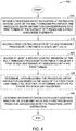
- Figure 4 is a flowchart illustrating a method performed by a multithreaded processor executing a plurality of threads, according to one or more embodiments disclosed herein.
- method 400 may be used in conjunction with a multithreaded processor, such as the multithreaded processor 100 depicted in Figure 2 .
- Method 400 begins at block 405, where a procedure entry instruction is received at instruction decode logic of the multithreaded processor.
- the procedure entry instruction corresponds to a first thread of the plurality of threads associated with the multithreaded processor, and the first thread is associated with a stack within a memory.
- the multithreaded processor accesses a first control register to retrieve a stack limit value.
- a designated stack limit value register stores the stack limit value.
- the stack limit value and/or the stack limit value register is shared by some or all of the plurality of threads.
- the multithreaded processor accesses at least a second control register to retrieve a value of a first stack limit enable bit associated with the first thread.
- the first stack limit enable bit generally indicates whether an updated stack pointer value will be checked against the stack limit value.
- the multithreaded processor determines, upon receiving the procedure entry instruction and based on the value of the first stack limit enable bit, whether to determine whether to throw the stack limit exception. In some embodiments, when the first stack limit enable bit is set, the multithreaded processor determines to check the updated stack pointer value against the stack limit value. When the first stack limit enable bit is cleared, the updated stack pointer value need not be checked.
- the first stack limit enable bit serves as an indicator for which stack region size regime within which the associated thread is operating. For example, when the first stack limit enable bit is set, the stack is included in a memory region associated with a default stack region size. When the first stack limit enable bit is cleared, the stack is included in another memory region associated with a larger stack region size. In alternate embodiments, a stack region size for the stack may be adaptively selected from more than two predefined stack region sizes.
- the multithreaded processor determines whether to throw a stack limit exception based on the stack limit value and a first predefined stack region size associated with the stack. Method 400 ends following completion of block 445.
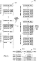
- Figure 5 illustrates a reassignment of a stack from a first stack region size to a second stack region size, according to one or more embodiments disclosed herein.
- diagram 500 may represent reassignment of the stack between different portions of a memory, such as the memory 235 of Figure 2 .
- the memory includes a first portion 502 comprising a plurality of first memory pages 505(1), 505(2), ..., 505(m), and a second portion 528 comprising a plurality of second memory pages 530(1), 530(2), ..., 530(p).
- Alternate embodiments may include a different sizing for the memory pages 505(i) and/or 530(j).
- the first portion 502 and the second portion 528 are each shown as including contiguous memory pages, alternate embodiments may include non-contiguous memory pages.
- Each of the first memory pages 505(1), 505(2), ..., 505(m) corresponds to a first stack region size 550
- each of the second memory pages 530(1), 530(2), ..., 530(p) corresponds to a second stack region size 555.
- the first stack region size 550 is the default stack region size 250 of Figure 2
- the second stack region size 555 is the larger stack region size 255 of Figure 2 .
- the first stack region size 550 is 2 kB and the second stack region size 555 is 8 kB, though other values are possible.
- Each of the first memory pages 505(1), 505(2), ..., 505(m) includes a number of memory regions 510, 515, 520 of the first stack region size 550, and at least one other memory region 512, 517, 522.
- the other memory region 512, 517, 522 may be sized based on a difference between the first stack region size 550 and the second stack region size 555, such that a sum of the first stack region size 550 and the size of the other memory region 512, 517, 522 at least equals the second stack region size 555.
- each first memory page 505(1), 505(2), ..., 505(m) is divided between twenty-nine (29) regions 510(1)-510(29), 515(1)-515(29), 520(1)-520(29) of 2 kB, and one other region 512, 517, 520 of 6 kB.
- Including the 6kB other memory region 512, 517, 522 ensures that each 2kB memory region 510(1)-510(29), 515(1)-515(29), 520(1)-520(29) can be mapped into a corresponding 8kB within the second memory pages 530(1), 530(2), ..., 530(p) while maintaining the same offset within the first memory page and the second memory page.
- the other memory region 512, 517, 522 generally permits an address in the virtual space to be translated into an address in the physical space. If a particular stack (included in a memory region 510, 515, 520) needs to grow beyond the 2 kB limit, the 6 kB of the other memory region 512, 517, 522 allows a total of 8 kB, without requiring an adjustment of the offset of the stack pointer.
- the appropriately sized other memory region 512, 517, 522 simplifies the reassignment of a stack from a first memory page 505(1), 505(2), ..., 505(m) to a second memory page 530(1), 530(2), ..., 530(p), as the data may be moved and an associated page mapping (e.g., in a MMU) updated without requiring performing additional processing of the stack.
- the stack reassignment may be performed without the complexity of scanning the contents of the stack and fixing up addresses included therein.
- Each of the second memory pages 530(1), 530(2), ..., 530(p) includes a number of memory regions 535, 540, 545. As shown, the 64kB of each second memory page 530(1), 530(2), ..., 530(p) is divided between thirty-two (32) regions 535(1)-535(32), 540(1)-540(32), 545(1)-545(32) of 2 kB each. Within each second memory page 530(1), 530(2), ..., 530(p), a 2 kB region from a first memory page 505(1), 505(2), ..., 505(m) is mapped into a block of four (4) contiguous regions 535, 540, 545 with an arbitrary 2 kB alignment. The block of four (4) contiguous regions corresponds to the second stack region size 555 - here, four contiguous 2 kB regions corresponds to the 8 kB second stack region size.
- the exception handler determines whether an 8 kB block having a top-most region at index (28) of a second memory page 530(1), 530(2), ..., 530(p) is available.
- a bitmap array e.g., bitmap array 232 of Figure 2
- the exception handler accesses the bitmap array to determine whether a suitable block is available.
- Bitmap array 232(1) shows a state of the bitmap array at a first time prior to reassigning the stack at region 515(28) to a second memory page.
- Each of entries 560(1), 560(2), ... 560(p) of the bitmap array are zeroed at the first time, indicating that none of the 2 kB regions included in pages 1-p (that is, the second memory pages 530(1)-530(p)) are occupied.
- the bitmap array 232(2) shows the updated bitmap array at a second time after reassigning the stack to the second memory page 530(2). As shown, entry 565(2) corresponding to the second memory page 530(2) has a hex value of "0000001 E".
- memory regions 540(25)-540(28) correspond to a hex value of "1” and memory regions 540(29)-540(32) correspond to a hex value of "E", collectively indicating that a block of memory regions 540(28), 540(29), 540(30), and 540(31) are occupied by the reassigned stack.
- the block is offset from the base of second memory page 530(2) by a single 2 kB region 540(32).
- the exception handler searches the bitmap array for a contiguous block of 2 kB regions within the second memory pages 530(1), 530(2), ..., 530(p) that match the alignment of the 2 kB region from the first memory page 505(1), 505(2), ..., 505(m).
- shared memory techniques are used to indivisibly update the bitmap array.
- a region from a first memory page 505(1), 505(2), ..., 505(m) can be copied into a highest-numbered region in a second memory page 530(1), 530(2), ..., 530(p) and the thread can resume its operation.
- Table 1 included below, includes exemplary pseudocode for reassigning a stack from a first memory page 505(1), 505(2), ..., 505(m) to a second memory page 530(1), 530(2), ..., 530(p). TABLE 1 Example pseudocode for reassigning a stack from a first memory page to a second memory page Assumptions: A.
- the 6 kB reserved region ensures that an 8 kB region will exist in a large stack page and that the 8 kB region will not span a page boundary.
- B. An array of 2 kB large stack components in 64 kB physical address pages, each page containing (32) 2 kB-aligned 2 kB regions. Four (4) contiguous components with an arbitrary 2 kB alignment within a large stack page form an 8 kB large stack.
- bitmaps An array of bitmaps, where each bitmap is associated with a specific large stack page and each bit in the bitmap corresponds to a 2 kB region in the page.
- Pseudocode 1. Locate target page. a. Obtain a lock to manipulate the bitmap array using a spin lock or other algorithm known to those skilled in the art. b. Compute a binary value corresponding to the 2 kB components of the 8 kB region in a large stack page for the small stack to be migrated. This is the large stack bit mask. c.
- Loop over the elements in the array of bitmaps (1) Compute the bitwise logical AND of the large stack bit mask and the 1's complemented current bitmap array element. (2) If the result of the bitwise logical AND is equal to the large stack bit mask then the large stack page corresponding to the current element will be the target page and exit the loop. d. If no target page was found, release the lock and return to step 1 to re-acquire the lock and repeat the loop. e. If a target page was found, logically OR the large stack bit mask into the associated bitmap element. f. Release the lock. 2. Move page data. a.
- the stack may no longer require the additional memory provided within the second memory page 530(1), 530(2), ..., 530(p), such as after the thread returns from a subroutine. In such a case, it may be beneficial to return the stack to a first memory page 505(1), 505(2), ..., 505(m) to free up the second memory pages 530(1), 530(2), ..., 530(p) for handling subsequent stack limit exceptions.
- the stack when a particular thread returns to its main (or parent) subroutine, the stack is reassigned (or migrated or moved) from a second memory page 530(1), 530(2), ..., 530(p) to a first memory page 505(1), 505(2), ..., 505(m).
- the stack upon returning from subroutine S2 to S1 the stack is reassigned to a first memory page 505(1), 505(2), ..., 505(m).
- the stack is reassigned upon determining that the thread has returned from the particular subroutine which caused the updated SP value to be less than the stack limit value (e.g., returned from subroutine S3 to S2).
- the multithreaded processor determines whether the stack limit enable bit for the stack is set. If the stack limit enable bit is cleared (e.g., indicating that the stack is included in a second memory page 530(1), 530(2), ..., 530(p)), the multithreaded processor migrates the 2 kB region at the highest address of the 8 kB block back to the first memory page 505(1), 505(2), ..., 505(m), clears the associated bits of the bitmap array, and sets the stack limit enable bit. The thread is thus configured to use the memory region within the first memory page 505(1), 505(2), ..., 505(m) until a subsequent stack limit exception.
- the stack limit enable bit is cleared (e.g., indicating that the stack is included in a second memory page 530(1), 530(2), ..., 530(p))
- the multithreaded processor migrates the 2 kB region at the highest address of the 8 kB block back to the first memory page 505(1), 505(2)
- Table 2 includes exemplary pseudocode for reassigning a stack from a second memory page 530(1), 530(2), ..., 530(p) to a first memory page 505(1), 505(2), ..., 505(m).
- Table 2 Example pseudocode for reassigning a stack from a second memory page to a first memory page Assumptions: A. An array of 2 kB small stack regions in 64 kB physical address pages, each page containing (29) 2 kB-aligned 2 kB regions, with a 6 kB region reserved at the base (lowest address) of the page.
- the 6 kB reserved region insures that an 8 kB region will exist in a large stack page and that the 8 kB region will not span a page boundary.
- C An array of bitmaps, where each bitmap is associated with a specific large stack page and each bit in the bitmap corresponds to a 2 kB region in the page.
- Pseudo-Code 1. Move page data. a.
- Figure 6 is a flowchart illustrating a method performed by a multithreaded processor executing a plurality of threads, according to one or more embodiments disclosed herein.
- method 600 may be used in conjunction with a multithreaded processor, such as the multithreaded processor 100 depicted in Figure 2 .
- Method 600 may further be used in conjunction with any of the embodiments discussed herein.
- Method 600 begins at block 605, where a procedure entry instruction associated is received.
- the procedure entry instruction is associated with a first thread of a plurality of threads.
- the multithreaded processor determines, based on a first stack limit enable bit associated with the first thread, whether to check an updated size of the first stack against a first predefined stack region size. If the first stack limit enable bit (EN) is cleared at block 615 ("NO"), the method proceeds to block 650 and the procedure entry instruction is executed.
- EN first stack limit enable bit
- the method proceeds to block 620 and the multithreaded processor checks the updated size of the first stack against the first predefined stack region size. If the updated size does not exceed the first predefined stack region sizeat block 625 ("NO"), the method proceeds to block 650 and the procedure entry instruction is executed.
- the method proceeds to block 630 and the multithreaded processor throws a stack limit exception.
- the multithreaded processor (such as an exception handler) reassigns the first stack from a first memory region of a first predefined stack region size to a second memory region of a second predefined stack region size.
- the second predefined stack region size is greater than the first predefined stack region size.
- the multithreaded processor updates a bitmap array to reflect a location of the first stack within the second memory region.
- the multithreaded processor clears the first stack limit enable bit.
- the multithreaded processor executes the procedure entry instruction.
- the first thread returns to a main subroutine.
- the method terminates.
- the multithreaded processor at block 665 reassigns a portion of the second memory region corresponding to the first predefined stack region size to the first memory region.
- the multithreaded processor updates the bitmap array to reflect the reassignment of the first stack to the first memory region.
- the multithreaded processor sets the first stack limit enable bit and the method terminates.
- aspects disclosed herein may be embodied as a system, method or computer program product. Accordingly, aspects may take the form of an entirely hardware embodiment, an entirely software embodiment (including firmware, resident software, micro-code, etc.) or an embodiment combining software and hardware aspects that may all generally be referred to herein as a "circuit,” “module” or “system.” Furthermore, aspects may take the form of a computer program product embodied in one or more computer readable medium(s) having computer readable program code embodied thereon.
- the computer readable medium may be a computer readable signal medium or a computer readable storage medium.
- a computer readable storage medium may be, for example, but not limited to, an electronic, magnetic, optical, electromagnetic, infrared, or semiconductor system, apparatus, or device, or any suitable combination of the foregoing.
- a computer readable storage medium is any tangible medium that can contain, or store a program for use by or in connection with an instruction execution system, apparatus or device.
- a computer readable signal medium may include a propagated data signal with computer readable program code embodied therein, for example, in baseband or as part of a carrier wave. Such a propagated signal may take any of a variety of forms, including, but not limited to, electro-magnetic, optical, or any suitable combination thereof.
- a computer readable signal medium may be any computer readable medium that is not a computer readable storage medium and that can communicate, propagate, or transport a program for use by or in connection with an instruction execution system, apparatus, or device.
- Program code embodied on a computer readable medium may be transmitted using any appropriate medium, including but not limited to wireless, wireline, optical fiber cable, RF, etc., or any suitable combination of the foregoing.
- Computer program code for carrying out operations for aspects of the present disclosure may be written in any combination of one or more programming languages, including an object oriented programming language such as Java, Smalltalk, C++ or the like and conventional procedural programming languages, such as the "C" programming language or similar programming languages.
- the program code may execute entirely on the user's computer, partly on the user's computer, as a stand-alone software package, partly on the user's computer and partly on a remote computer or entirely on the remote computer or server.
- the remote computer may be connected to the user's computer through any type of network, including a local area network (LAN) or a wide area network (WAN), or the connection may be made to an external computer (for example, through the Internet using an Internet Service Provider).
- LAN local area network
- WAN wide area network
- Internet Service Provider for example, AT&T, MCI, Sprint, EarthLink, MSN, GTE, etc.
- These computer program instructions may also be stored in a computer readable medium that can direct a computer, other programmable data processing apparatus, or other devices to function in a particular manner, such that the instructions stored in the computer readable medium produce an article of manufacture including instructions which implement the function/act specified in the flowchart and/or block diagram block or blocks.
- the computer program instructions may also be loaded onto a computer, other programmable data processing apparatus, or other devices to cause a series of operational steps to be performed on the computer, other programmable apparatus or other devices to produce a computer implemented process such that the instructions which execute on the computer or other programmable apparatus provide processes for implementing the functions/acts specified in the flowchart and/or block diagram block or blocks.
- each block in the flowchart or block diagrams may represent a module, segment or portion of code, which comprises one or more executable instructions for implementing the specified logical function(s).
- the functions noted in the block may occur out of the order noted in the figures. For example, two blocks shown in succession may, in fact, be executed substantially concurrently, or the blocks may sometimes be executed in the reverse order, depending upon the functionality involved.
- Embodiments are generally directed to a multithreaded processor for executing a plurality of threads, as well as an associated method and system.
- the multithreaded processor comprises a first control register configured to store a stack limit value, and instruction decode logic configured to, upon receiving a procedure entry instruction for a stack associated with a first thread, determine whether to throw a stack limit exception based on the stack limit value and a first predefined stack region size associated with the stack.
Landscapes
- Engineering & Computer Science (AREA)
- Software Systems (AREA)
- Theoretical Computer Science (AREA)
- Physics & Mathematics (AREA)
- General Engineering & Computer Science (AREA)
- General Physics & Mathematics (AREA)
- Multimedia (AREA)
- Memory System Of A Hierarchy Structure (AREA)
- Executing Machine-Instructions (AREA)
- Debugging And Monitoring (AREA)
Applications Claiming Priority (1)
| Application Number | Priority Date | Filing Date | Title |
|---|---|---|---|
| US15/367,008 US10649786B2 (en) | 2016-12-01 | 2016-12-01 | Reduced stack usage in a multithreaded processor |
Publications (3)
| Publication Number | Publication Date |
|---|---|
| EP3330848A2 true EP3330848A2 (de) | 2018-06-06 |
| EP3330848A3 EP3330848A3 (de) | 2018-07-18 |
| EP3330848B1 EP3330848B1 (de) | 2022-07-20 |
Family
ID=59409244
Family Applications (1)
| Application Number | Title | Priority Date | Filing Date |
|---|---|---|---|
| EP17183239.7A Active EP3330848B1 (de) | 2016-12-01 | 2017-07-26 | Erkennung von stapelspeicherüberlauf in einem multithread-prozessor |
Country Status (2)
| Country | Link |
|---|---|
| US (1) | US10649786B2 (de) |
| EP (1) | EP3330848B1 (de) |
Families Citing this family (2)
| Publication number | Priority date | Publication date | Assignee | Title |
|---|---|---|---|---|
| US10866806B2 (en) * | 2017-11-14 | 2020-12-15 | Nvidia Corporation | Uniform register file for improved resource utilization |
| US11782762B2 (en) * | 2019-02-27 | 2023-10-10 | Qualcomm Incorporated | Stack management |
Family Cites Families (10)
| Publication number | Priority date | Publication date | Assignee | Title |
|---|---|---|---|---|
| JPS6057439A (ja) | 1983-09-08 | 1985-04-03 | Matsushita Electric Ind Co Ltd | スタツクあふれ検出装置 |
| JPH01255035A (ja) | 1988-04-05 | 1989-10-11 | Matsushita Electric Ind Co Ltd | プロセサ |
| JPH02214938A (ja) | 1989-02-15 | 1990-08-27 | Hitachi Ltd | データ処理装置 |
| JP3739797B2 (ja) * | 1995-10-06 | 2006-01-25 | パトリオット サイエンティフィック コーポレイション | 縮小命令セット・コンピューター・マイクロプロセッサーの構造 |
| US7178002B2 (en) | 2002-07-24 | 2007-02-13 | Sun Microsystems, Inc. | Methods and systems for dynamically growing multiple stacks |
| US20070282928A1 (en) * | 2006-06-06 | 2007-12-06 | Guofang Jiao | Processor core stack extension |
| US20120017214A1 (en) | 2010-07-16 | 2012-01-19 | Qualcomm Incorporated | System and method to allocate portions of a shared stack |
| US8566935B2 (en) * | 2011-05-12 | 2013-10-22 | At&T Intellectual Property I, L.P. | Balancing malware rootkit detection with power consumption on mobile devices |
| FR3013869B1 (fr) * | 2013-11-22 | 2016-01-01 | Thales Sa | Procede de detection des debordements de pile et processeur pour la mise en oeuvre d'un tel procede |
| US9483272B2 (en) * | 2014-09-30 | 2016-11-01 | Freescale Semiconductor, Inc. | Systems and methods for managing return stacks in a multi-threaded data processing system |
-
2016
- 2016-12-01 US US15/367,008 patent/US10649786B2/en active Active
-
2017
- 2017-07-26 EP EP17183239.7A patent/EP3330848B1/de active Active
Non-Patent Citations (1)
| Title |
|---|
| None |
Also Published As
| Publication number | Publication date |
|---|---|
| US10649786B2 (en) | 2020-05-12 |
| US20180157493A1 (en) | 2018-06-07 |
| EP3330848A3 (de) | 2018-07-18 |
| EP3330848B1 (de) | 2022-07-20 |
Similar Documents
| Publication | Publication Date | Title |
|---|---|---|
| US7487327B1 (en) | Processor and method for device-specific memory address translation | |
| US7426626B2 (en) | TLB lock indicator | |
| US8566563B2 (en) | Translation table control | |
| US8156309B2 (en) | Translation look-aside buffer with variable page sizes | |
| US7461209B2 (en) | Transient cache storage with discard function for disposable data | |
| CN1304962C (zh) | 转译后备缓冲器清除滤波器 | |
| US9152572B2 (en) | Translation lookaside buffer for multiple context compute engine | |
| US9779028B1 (en) | Managing translation invalidation | |
| US8645666B2 (en) | Means to share translation lookaside buffer (TLB) entries between different contexts | |
| US9886385B1 (en) | Content-directed prefetch circuit with quality filtering | |
| US11176055B1 (en) | Managing potential faults for speculative page table access | |
| JP2735781B2 (ja) | キャッシュ・メモリ制御システム及び方法 | |
| JP2019532450A (ja) | 巨大ページをサポートするメモリ管理 | |
| KR102026877B1 (ko) | 메모리 관리 유닛 및 그 동작 방법 | |
| JPH0619793A (ja) | キャッシュ・アクセスのための仮想アドレス変換予測の履歴テーブル | |
| US10915459B2 (en) | Methods and systems for optimized translation of a virtual address having multiple virtual address portions using multiple translation lookaside buffer (TLB) arrays for variable page sizes | |
| JP2001195303A (ja) | 機能が並列に分散された変換索引バッファ | |
| US11775445B2 (en) | Translation support for a virtual cache | |
| US7093100B2 (en) | Translation look aside buffer (TLB) with increased translational capacity for multi-threaded computer processes | |
| EP1139222A1 (de) | Vorausladung für TLB-Cachespeicher | |
| JP5916355B2 (ja) | プログラムの命令を実行する装置および命令をキャッシュするシステム | |
| EP2159707A1 (de) | Arithmetische verarbeitungseinheit, eingangs-steuerprogramm und eingangs-steuerverfahren | |
| EP3330848B1 (de) | Erkennung von stapelspeicherüberlauf in einem multithread-prozessor | |
| US8266379B2 (en) | Multithreaded processor with multiple caches | |
| US10146698B2 (en) | Method and apparatus for power reduction in a multi-threaded mode |
Legal Events
| Date | Code | Title | Description |
|---|---|---|---|
| PUAI | Public reference made under article 153(3) epc to a published international application that has entered the european phase |
Free format text: ORIGINAL CODE: 0009012 |
|
| STAA | Information on the status of an ep patent application or granted ep patent |
Free format text: STATUS: THE APPLICATION HAS BEEN PUBLISHED |
|
| AK | Designated contracting states |
Kind code of ref document: A2 Designated state(s): AL AT BE BG CH CY CZ DE DK EE ES FI FR GB GR HR HU IE IS IT LI LT LU LV MC MK MT NL NO PL PT RO RS SE SI SK SM TR |
|
| AX | Request for extension of the european patent |
Extension state: BA ME |
|
| PUAL | Search report despatched |
Free format text: ORIGINAL CODE: 0009013 |
|
| AK | Designated contracting states |
Kind code of ref document: A3 Designated state(s): AL AT BE BG CH CY CZ DE DK EE ES FI FR GB GR HR HU IE IS IT LI LT LU LV MC MK MT NL NO PL PT RO RS SE SI SK SM TR |
|
| AX | Request for extension of the european patent |
Extension state: BA ME |
|
| RIC1 | Information provided on ipc code assigned before grant |
Ipc: G06F 9/50 20060101ALI20180613BHEP Ipc: G06F 9/448 20180101ALI20180613BHEP Ipc: G06F 9/30 20180101ALI20180613BHEP Ipc: G06F 9/38 20180101AFI20180613BHEP |
|
| STAA | Information on the status of an ep patent application or granted ep patent |
Free format text: STATUS: REQUEST FOR EXAMINATION WAS MADE |
|
| 17P | Request for examination filed |
Effective date: 20190118 |
|
| RBV | Designated contracting states (corrected) |
Designated state(s): AL AT BE BG CH CY CZ DE DK EE ES FI FR GB GR HR HU IE IS IT LI LT LU LV MC MK MT NL NO PL PT RO RS SE SI SK SM TR |
|
| STAA | Information on the status of an ep patent application or granted ep patent |
Free format text: STATUS: EXAMINATION IS IN PROGRESS |
|
| 17Q | First examination report despatched |
Effective date: 20200114 |
|
| GRAP | Despatch of communication of intention to grant a patent |
Free format text: ORIGINAL CODE: EPIDOSNIGR1 |
|
| STAA | Information on the status of an ep patent application or granted ep patent |
Free format text: STATUS: GRANT OF PATENT IS INTENDED |
|
| INTG | Intention to grant announced |
Effective date: 20220221 |
|
| GRAS | Grant fee paid |
Free format text: ORIGINAL CODE: EPIDOSNIGR3 |
|
| GRAA | (expected) grant |
Free format text: ORIGINAL CODE: 0009210 |
|
| STAA | Information on the status of an ep patent application or granted ep patent |
Free format text: STATUS: THE PATENT HAS BEEN GRANTED |
|
| AK | Designated contracting states |
Kind code of ref document: B1 Designated state(s): AL AT BE BG CH CY CZ DE DK EE ES FI FR GB GR HR HU IE IS IT LI LT LU LV MC MK MT NL NO PL PT RO RS SE SI SK SM TR |
|
| REG | Reference to a national code |
Ref country code: CH Ref legal event code: EP |
|
| REG | Reference to a national code |
Ref country code: DE Ref legal event code: R096 Ref document number: 602017059591 Country of ref document: DE |
|
| REG | Reference to a national code |
Ref country code: AT Ref legal event code: REF Ref document number: 1505965 Country of ref document: AT Kind code of ref document: T Effective date: 20220815 |
|
| REG | Reference to a national code |
Ref country code: IE Ref legal event code: FG4D |
|
| REG | Reference to a national code |
Ref country code: LT Ref legal event code: MG9D |
|
| REG | Reference to a national code |
Ref country code: NL Ref legal event code: MP Effective date: 20220720 |
|
| PG25 | Lapsed in a contracting state [announced via postgrant information from national office to epo] |
Ref country code: SE Free format text: LAPSE BECAUSE OF FAILURE TO SUBMIT A TRANSLATION OF THE DESCRIPTION OR TO PAY THE FEE WITHIN THE PRESCRIBED TIME-LIMIT Effective date: 20220720 Ref country code: RS Free format text: LAPSE BECAUSE OF FAILURE TO SUBMIT A TRANSLATION OF THE DESCRIPTION OR TO PAY THE FEE WITHIN THE PRESCRIBED TIME-LIMIT Effective date: 20220720 Ref country code: PT Free format text: LAPSE BECAUSE OF FAILURE TO SUBMIT A TRANSLATION OF THE DESCRIPTION OR TO PAY THE FEE WITHIN THE PRESCRIBED TIME-LIMIT Effective date: 20221121 Ref country code: NO Free format text: LAPSE BECAUSE OF FAILURE TO SUBMIT A TRANSLATION OF THE DESCRIPTION OR TO PAY THE FEE WITHIN THE PRESCRIBED TIME-LIMIT Effective date: 20221020 Ref country code: NL Free format text: LAPSE BECAUSE OF FAILURE TO SUBMIT A TRANSLATION OF THE DESCRIPTION OR TO PAY THE FEE WITHIN THE PRESCRIBED TIME-LIMIT Effective date: 20220720 Ref country code: LV Free format text: LAPSE BECAUSE OF FAILURE TO SUBMIT A TRANSLATION OF THE DESCRIPTION OR TO PAY THE FEE WITHIN THE PRESCRIBED TIME-LIMIT Effective date: 20220720 Ref country code: LT Free format text: LAPSE BECAUSE OF FAILURE TO SUBMIT A TRANSLATION OF THE DESCRIPTION OR TO PAY THE FEE WITHIN THE PRESCRIBED TIME-LIMIT Effective date: 20220720 Ref country code: FI Free format text: LAPSE BECAUSE OF FAILURE TO SUBMIT A TRANSLATION OF THE DESCRIPTION OR TO PAY THE FEE WITHIN THE PRESCRIBED TIME-LIMIT Effective date: 20220720 Ref country code: ES Free format text: LAPSE BECAUSE OF FAILURE TO SUBMIT A TRANSLATION OF THE DESCRIPTION OR TO PAY THE FEE WITHIN THE PRESCRIBED TIME-LIMIT Effective date: 20220720 |
|
| REG | Reference to a national code |
Ref country code: DE Ref legal event code: R119 Ref document number: 602017059591 Country of ref document: DE |
|
| REG | Reference to a national code |
Ref country code: AT Ref legal event code: MK05 Ref document number: 1505965 Country of ref document: AT Kind code of ref document: T Effective date: 20220720 |
|
| PG25 | Lapsed in a contracting state [announced via postgrant information from national office to epo] |
Ref country code: PL Free format text: LAPSE BECAUSE OF FAILURE TO SUBMIT A TRANSLATION OF THE DESCRIPTION OR TO PAY THE FEE WITHIN THE PRESCRIBED TIME-LIMIT Effective date: 20220720 Ref country code: IS Free format text: LAPSE BECAUSE OF FAILURE TO SUBMIT A TRANSLATION OF THE DESCRIPTION OR TO PAY THE FEE WITHIN THE PRESCRIBED TIME-LIMIT Effective date: 20221120 Ref country code: HR Free format text: LAPSE BECAUSE OF FAILURE TO SUBMIT A TRANSLATION OF THE DESCRIPTION OR TO PAY THE FEE WITHIN THE PRESCRIBED TIME-LIMIT Effective date: 20220720 Ref country code: GR Free format text: LAPSE BECAUSE OF FAILURE TO SUBMIT A TRANSLATION OF THE DESCRIPTION OR TO PAY THE FEE WITHIN THE PRESCRIBED TIME-LIMIT Effective date: 20221021 |
|
| REG | Reference to a national code |
Ref country code: CH Ref legal event code: PL |
|
| REG | Reference to a national code |
Ref country code: BE Ref legal event code: MM Effective date: 20220731 |
|
| REG | Reference to a national code |
Ref country code: DE Ref legal event code: R097 Ref document number: 602017059591 Country of ref document: DE |
|
| PG25 | Lapsed in a contracting state [announced via postgrant information from national office to epo] |
Ref country code: SM Free format text: LAPSE BECAUSE OF FAILURE TO SUBMIT A TRANSLATION OF THE DESCRIPTION OR TO PAY THE FEE WITHIN THE PRESCRIBED TIME-LIMIT Effective date: 20220720 Ref country code: RO Free format text: LAPSE BECAUSE OF FAILURE TO SUBMIT A TRANSLATION OF THE DESCRIPTION OR TO PAY THE FEE WITHIN THE PRESCRIBED TIME-LIMIT Effective date: 20220720 Ref country code: MC Free format text: LAPSE BECAUSE OF FAILURE TO SUBMIT A TRANSLATION OF THE DESCRIPTION OR TO PAY THE FEE WITHIN THE PRESCRIBED TIME-LIMIT Effective date: 20220720 Ref country code: LU Free format text: LAPSE BECAUSE OF NON-PAYMENT OF DUE FEES Effective date: 20220726 Ref country code: LI Free format text: LAPSE BECAUSE OF NON-PAYMENT OF DUE FEES Effective date: 20220731 Ref country code: DK Free format text: LAPSE BECAUSE OF FAILURE TO SUBMIT A TRANSLATION OF THE DESCRIPTION OR TO PAY THE FEE WITHIN THE PRESCRIBED TIME-LIMIT Effective date: 20220720 Ref country code: CZ Free format text: LAPSE BECAUSE OF FAILURE TO SUBMIT A TRANSLATION OF THE DESCRIPTION OR TO PAY THE FEE WITHIN THE PRESCRIBED TIME-LIMIT Effective date: 20220720 Ref country code: CH Free format text: LAPSE BECAUSE OF NON-PAYMENT OF DUE FEES Effective date: 20220731 Ref country code: AT Free format text: LAPSE BECAUSE OF FAILURE TO SUBMIT A TRANSLATION OF THE DESCRIPTION OR TO PAY THE FEE WITHIN THE PRESCRIBED TIME-LIMIT Effective date: 20220720 |
|
| PLBE | No opposition filed within time limit |
Free format text: ORIGINAL CODE: 0009261 |
|
| STAA | Information on the status of an ep patent application or granted ep patent |
Free format text: STATUS: NO OPPOSITION FILED WITHIN TIME LIMIT |
|
| PG25 | Lapsed in a contracting state [announced via postgrant information from national office to epo] |
Ref country code: SK Free format text: LAPSE BECAUSE OF FAILURE TO SUBMIT A TRANSLATION OF THE DESCRIPTION OR TO PAY THE FEE WITHIN THE PRESCRIBED TIME-LIMIT Effective date: 20220720 Ref country code: EE Free format text: LAPSE BECAUSE OF FAILURE TO SUBMIT A TRANSLATION OF THE DESCRIPTION OR TO PAY THE FEE WITHIN THE PRESCRIBED TIME-LIMIT Effective date: 20220720 Ref country code: DE Free format text: LAPSE BECAUSE OF NON-PAYMENT OF DUE FEES Effective date: 20230201 Ref country code: BE Free format text: LAPSE BECAUSE OF NON-PAYMENT OF DUE FEES Effective date: 20220731 |
|
| 26N | No opposition filed |
Effective date: 20230421 |
|
| PG25 | Lapsed in a contracting state [announced via postgrant information from national office to epo] |
Ref country code: AL Free format text: LAPSE BECAUSE OF FAILURE TO SUBMIT A TRANSLATION OF THE DESCRIPTION OR TO PAY THE FEE WITHIN THE PRESCRIBED TIME-LIMIT Effective date: 20220720 |
|
| P01 | Opt-out of the competence of the unified patent court (upc) registered |
Effective date: 20230525 |
|
| REG | Reference to a national code |
Ref country code: DE Ref legal event code: R073 Ref document number: 602017059591 Country of ref document: DE |
|
| REG | Reference to a national code |
Ref country code: DE Ref legal event code: R074 Ref document number: 602017059591 Country of ref document: DE |
|
| PG25 | Lapsed in a contracting state [announced via postgrant information from national office to epo] |
Ref country code: IE Free format text: LAPSE BECAUSE OF NON-PAYMENT OF DUE FEES Effective date: 20220726 |
|
| PG25 | Lapsed in a contracting state [announced via postgrant information from national office to epo] |
Ref country code: SI Free format text: LAPSE BECAUSE OF FAILURE TO SUBMIT A TRANSLATION OF THE DESCRIPTION OR TO PAY THE FEE WITHIN THE PRESCRIBED TIME-LIMIT Effective date: 20220720 |
|
| PG25 | Lapsed in a contracting state [announced via postgrant information from national office to epo] |
Ref country code: DE Free format text: LAPSE BECAUSE OF NON-PAYMENT OF DUE FEES Effective date: 20230201 |
|
| PGRI | Patent reinstated in contracting state [announced from national office to epo] |
Ref country code: DE Effective date: 20230729 |
|
| PG25 | Lapsed in a contracting state [announced via postgrant information from national office to epo] |
Ref country code: HU Free format text: LAPSE BECAUSE OF FAILURE TO SUBMIT A TRANSLATION OF THE DESCRIPTION OR TO PAY THE FEE WITHIN THE PRESCRIBED TIME-LIMIT; INVALID AB INITIO Effective date: 20170726 |
|
| PG25 | Lapsed in a contracting state [announced via postgrant information from national office to epo] |
Ref country code: MK Free format text: LAPSE BECAUSE OF FAILURE TO SUBMIT A TRANSLATION OF THE DESCRIPTION OR TO PAY THE FEE WITHIN THE PRESCRIBED TIME-LIMIT Effective date: 20220720 Ref country code: CY Free format text: LAPSE BECAUSE OF FAILURE TO SUBMIT A TRANSLATION OF THE DESCRIPTION OR TO PAY THE FEE WITHIN THE PRESCRIBED TIME-LIMIT Effective date: 20220720 |
|
| PG25 | Lapsed in a contracting state [announced via postgrant information from national office to epo] |
Ref country code: IT Free format text: LAPSE BECAUSE OF FAILURE TO SUBMIT A TRANSLATION OF THE DESCRIPTION OR TO PAY THE FEE WITHIN THE PRESCRIBED TIME-LIMIT Effective date: 20220720 |
|
| PG25 | Lapsed in a contracting state [announced via postgrant information from national office to epo] |
Ref country code: BG Free format text: LAPSE BECAUSE OF FAILURE TO SUBMIT A TRANSLATION OF THE DESCRIPTION OR TO PAY THE FEE WITHIN THE PRESCRIBED TIME-LIMIT Effective date: 20220720 |
|
| PG25 | Lapsed in a contracting state [announced via postgrant information from national office to epo] |
Ref country code: MT Free format text: LAPSE BECAUSE OF FAILURE TO SUBMIT A TRANSLATION OF THE DESCRIPTION OR TO PAY THE FEE WITHIN THE PRESCRIBED TIME-LIMIT Effective date: 20220720 |
|
| PGFP | Annual fee paid to national office [announced via postgrant information from national office to epo] |
Ref country code: DE Payment date: 20250618 Year of fee payment: 9 |
|
| PGFP | Annual fee paid to national office [announced via postgrant information from national office to epo] |
Ref country code: GB Payment date: 20250711 Year of fee payment: 9 |
|
| PGFP | Annual fee paid to national office [announced via postgrant information from national office to epo] |
Ref country code: FR Payment date: 20250716 Year of fee payment: 9 |
|
| PG25 | Lapsed in a contracting state [announced via postgrant information from national office to epo] |
Ref country code: TR Free format text: LAPSE BECAUSE OF FAILURE TO SUBMIT A TRANSLATION OF THE DESCRIPTION OR TO PAY THE FEE WITHIN THE PRESCRIBED TIME-LIMIT Effective date: 20220720 |