EP3321973B1 - Kristalline solarzelle mit einer transparenten, leitfähigen schicht zwischen den vorderseitenkontakten und verfahren zur herstellung einer solchen solarzelle - Google Patents
Kristalline solarzelle mit einer transparenten, leitfähigen schicht zwischen den vorderseitenkontakten und verfahren zur herstellung einer solchen solarzelle Download PDFInfo
- Publication number
- EP3321973B1 EP3321973B1 EP16197972.9A EP16197972A EP3321973B1 EP 3321973 B1 EP3321973 B1 EP 3321973B1 EP 16197972 A EP16197972 A EP 16197972A EP 3321973 B1 EP3321973 B1 EP 3321973B1
- Authority
- EP
- European Patent Office
- Prior art keywords
- electrically conductive
- semiconductor material
- layer
- solar cell
- conductive material
- Prior art date
- Legal status (The legal status is an assumption and is not a legal conclusion. Google has not performed a legal analysis and makes no representation as to the accuracy of the status listed.)
- Active
Links
Images


Classifications
-
- H—ELECTRICITY
- H10—SEMICONDUCTOR DEVICES; ELECTRIC SOLID-STATE DEVICES NOT OTHERWISE PROVIDED FOR
- H10F—INORGANIC SEMICONDUCTOR DEVICES SENSITIVE TO INFRARED RADIATION, LIGHT, ELECTROMAGNETIC RADIATION OF SHORTER WAVELENGTH OR CORPUSCULAR RADIATION
- H10F77/00—Constructional details of devices covered by this subclass
- H10F77/20—Electrodes
- H10F77/244—Electrodes made of transparent conductive layers, e.g. transparent conductive oxide [TCO] layers
-
- H—ELECTRICITY
- H10—SEMICONDUCTOR DEVICES; ELECTRIC SOLID-STATE DEVICES NOT OTHERWISE PROVIDED FOR
- H10F—INORGANIC SEMICONDUCTOR DEVICES SENSITIVE TO INFRARED RADIATION, LIGHT, ELECTROMAGNETIC RADIATION OF SHORTER WAVELENGTH OR CORPUSCULAR RADIATION
- H10F10/00—Individual photovoltaic cells, e.g. solar cells
- H10F10/10—Individual photovoltaic cells, e.g. solar cells having potential barriers
- H10F10/14—Photovoltaic cells having only PN homojunction potential barriers
-
- H—ELECTRICITY
- H10—SEMICONDUCTOR DEVICES; ELECTRIC SOLID-STATE DEVICES NOT OTHERWISE PROVIDED FOR
- H10F—INORGANIC SEMICONDUCTOR DEVICES SENSITIVE TO INFRARED RADIATION, LIGHT, ELECTROMAGNETIC RADIATION OF SHORTER WAVELENGTH OR CORPUSCULAR RADIATION
- H10F71/00—Manufacture or treatment of devices covered by this subclass
- H10F71/129—Passivating
-
- H—ELECTRICITY
- H10—SEMICONDUCTOR DEVICES; ELECTRIC SOLID-STATE DEVICES NOT OTHERWISE PROVIDED FOR
- H10F—INORGANIC SEMICONDUCTOR DEVICES SENSITIVE TO INFRARED RADIATION, LIGHT, ELECTROMAGNETIC RADIATION OF SHORTER WAVELENGTH OR CORPUSCULAR RADIATION
- H10F71/00—Manufacture or treatment of devices covered by this subclass
- H10F71/138—Manufacture of transparent electrodes, e.g. transparent conductive oxides [TCO] or indium tin oxide [ITO] electrodes
-
- H—ELECTRICITY
- H10—SEMICONDUCTOR DEVICES; ELECTRIC SOLID-STATE DEVICES NOT OTHERWISE PROVIDED FOR
- H10F—INORGANIC SEMICONDUCTOR DEVICES SENSITIVE TO INFRARED RADIATION, LIGHT, ELECTROMAGNETIC RADIATION OF SHORTER WAVELENGTH OR CORPUSCULAR RADIATION
- H10F77/00—Constructional details of devices covered by this subclass
- H10F77/20—Electrodes
- H10F77/206—Electrodes for devices having potential barriers
- H10F77/211—Electrodes for devices having potential barriers for photovoltaic cells
-
- H—ELECTRICITY
- H10—SEMICONDUCTOR DEVICES; ELECTRIC SOLID-STATE DEVICES NOT OTHERWISE PROVIDED FOR
- H10F—INORGANIC SEMICONDUCTOR DEVICES SENSITIVE TO INFRARED RADIATION, LIGHT, ELECTROMAGNETIC RADIATION OF SHORTER WAVELENGTH OR CORPUSCULAR RADIATION
- H10F77/00—Constructional details of devices covered by this subclass
- H10F77/20—Electrodes
- H10F77/206—Electrodes for devices having potential barriers
- H10F77/211—Electrodes for devices having potential barriers for photovoltaic cells
- H10F77/219—Arrangements for electrodes of back-contact photovoltaic cells
-
- H—ELECTRICITY
- H10—SEMICONDUCTOR DEVICES; ELECTRIC SOLID-STATE DEVICES NOT OTHERWISE PROVIDED FOR
- H10F—INORGANIC SEMICONDUCTOR DEVICES SENSITIVE TO INFRARED RADIATION, LIGHT, ELECTROMAGNETIC RADIATION OF SHORTER WAVELENGTH OR CORPUSCULAR RADIATION
- H10F77/00—Constructional details of devices covered by this subclass
- H10F77/20—Electrodes
- H10F77/244—Electrodes made of transparent conductive layers, e.g. transparent conductive oxide [TCO] layers
- H10F77/247—Electrodes made of transparent conductive layers, e.g. transparent conductive oxide [TCO] layers comprising indium tin oxide [ITO]
-
- H—ELECTRICITY
- H10—SEMICONDUCTOR DEVICES; ELECTRIC SOLID-STATE DEVICES NOT OTHERWISE PROVIDED FOR
- H10F—INORGANIC SEMICONDUCTOR DEVICES SENSITIVE TO INFRARED RADIATION, LIGHT, ELECTROMAGNETIC RADIATION OF SHORTER WAVELENGTH OR CORPUSCULAR RADIATION
- H10F77/00—Constructional details of devices covered by this subclass
- H10F77/20—Electrodes
- H10F77/244—Electrodes made of transparent conductive layers, e.g. transparent conductive oxide [TCO] layers
- H10F77/251—Electrodes made of transparent conductive layers, e.g. transparent conductive oxide [TCO] layers comprising zinc oxide [ZnO]
-
- H—ELECTRICITY
- H10—SEMICONDUCTOR DEVICES; ELECTRIC SOLID-STATE DEVICES NOT OTHERWISE PROVIDED FOR
- H10F—INORGANIC SEMICONDUCTOR DEVICES SENSITIVE TO INFRARED RADIATION, LIGHT, ELECTROMAGNETIC RADIATION OF SHORTER WAVELENGTH OR CORPUSCULAR RADIATION
- H10F77/00—Constructional details of devices covered by this subclass
- H10F77/30—Coatings
- H10F77/306—Coatings for devices having potential barriers
- H10F77/311—Coatings for devices having potential barriers for photovoltaic cells
-
- H—ELECTRICITY
- H10—SEMICONDUCTOR DEVICES; ELECTRIC SOLID-STATE DEVICES NOT OTHERWISE PROVIDED FOR
- H10F—INORGANIC SEMICONDUCTOR DEVICES SENSITIVE TO INFRARED RADIATION, LIGHT, ELECTROMAGNETIC RADIATION OF SHORTER WAVELENGTH OR CORPUSCULAR RADIATION
- H10F77/00—Constructional details of devices covered by this subclass
- H10F77/30—Coatings
- H10F77/306—Coatings for devices having potential barriers
- H10F77/311—Coatings for devices having potential barriers for photovoltaic cells
- H10F77/315—Coatings for devices having potential barriers for photovoltaic cells the coatings being antireflective or having enhancing optical properties
-
- H—ELECTRICITY
- H10—SEMICONDUCTOR DEVICES; ELECTRIC SOLID-STATE DEVICES NOT OTHERWISE PROVIDED FOR
- H10P—GENERIC PROCESSES OR APPARATUS FOR THE MANUFACTURE OR TREATMENT OF DEVICES COVERED BY CLASS H10
- H10P14/00—Formation of materials, e.g. in the shape of layers or pillars
- H10P14/20—Formation of materials, e.g. in the shape of layers or pillars of semiconductor materials
- H10P14/24—Formation of materials, e.g. in the shape of layers or pillars of semiconductor materials using chemical vapour deposition [CVD]
-
- H—ELECTRICITY
- H10—SEMICONDUCTOR DEVICES; ELECTRIC SOLID-STATE DEVICES NOT OTHERWISE PROVIDED FOR
- H10P—GENERIC PROCESSES OR APPARATUS FOR THE MANUFACTURE OR TREATMENT OF DEVICES COVERED BY CLASS H10
- H10P14/00—Formation of materials, e.g. in the shape of layers or pillars
- H10P14/40—Formation of materials, e.g. in the shape of layers or pillars of conductive or resistive materials
- H10P14/42—Formation of materials, e.g. in the shape of layers or pillars of conductive or resistive materials using a gas or vapour
- H10P14/43—Chemical deposition, e.g. chemical vapour deposition [CVD]
- H10P14/432—Chemical deposition, e.g. chemical vapour deposition [CVD] using selective deposition
-
- H—ELECTRICITY
- H10—SEMICONDUCTOR DEVICES; ELECTRIC SOLID-STATE DEVICES NOT OTHERWISE PROVIDED FOR
- H10P—GENERIC PROCESSES OR APPARATUS FOR THE MANUFACTURE OR TREATMENT OF DEVICES COVERED BY CLASS H10
- H10P14/00—Formation of materials, e.g. in the shape of layers or pillars
- H10P14/60—Formation of materials, e.g. in the shape of layers or pillars of insulating materials
- H10P14/63—Formation of materials, e.g. in the shape of layers or pillars of insulating materials characterised by the formation processes
- H10P14/6326—Deposition processes
- H10P14/6328—Deposition from the gas or vapour phase
- H10P14/6334—Deposition from the gas or vapour phase using decomposition or reaction of gaseous or vapour phase compounds, i.e. chemical vapour deposition
- H10P14/6336—Deposition from the gas or vapour phase using decomposition or reaction of gaseous or vapour phase compounds, i.e. chemical vapour deposition in the presence of a plasma [PECVD]
-
- H—ELECTRICITY
- H10—SEMICONDUCTOR DEVICES; ELECTRIC SOLID-STATE DEVICES NOT OTHERWISE PROVIDED FOR
- H10P—GENERIC PROCESSES OR APPARATUS FOR THE MANUFACTURE OR TREATMENT OF DEVICES COVERED BY CLASS H10
- H10P14/00—Formation of materials, e.g. in the shape of layers or pillars
- H10P14/60—Formation of materials, e.g. in the shape of layers or pillars of insulating materials
- H10P14/69—Inorganic materials
- H10P14/692—Inorganic materials composed of oxides, glassy oxides or oxide-based glasses
- H10P14/6938—Inorganic materials composed of oxides, glassy oxides or oxide-based glasses the material containing at least one metal element, e.g. metal oxides, metal oxynitrides or metal oxycarbides
-
- Y—GENERAL TAGGING OF NEW TECHNOLOGICAL DEVELOPMENTS; GENERAL TAGGING OF CROSS-SECTIONAL TECHNOLOGIES SPANNING OVER SEVERAL SECTIONS OF THE IPC; TECHNICAL SUBJECTS COVERED BY FORMER USPC CROSS-REFERENCE ART COLLECTIONS [XRACs] AND DIGESTS
- Y02—TECHNOLOGIES OR APPLICATIONS FOR MITIGATION OR ADAPTATION AGAINST CLIMATE CHANGE
- Y02E—REDUCTION OF GREENHOUSE GAS [GHG] EMISSIONS, RELATED TO ENERGY GENERATION, TRANSMISSION OR DISTRIBUTION
- Y02E10/00—Energy generation through renewable energy sources
- Y02E10/50—Photovoltaic [PV] energy
- Y02E10/547—Monocrystalline silicon PV cells
Definitions
- the invention relates to a crystalline solar cell made of a semiconductor material, which has a transparent, conductive layer between the electrical contacts on the front side, and a method for producing such a solar cell.
- Conventional Si solar cells consist of two oppositely doped areas of a monocrystalline or multicrystalline semiconductor material. A direct pn junction between the two regions is achieved by introducing dopants into the semiconductor material or by applying a layer of the same semiconductor material to a first layer of the semiconductor material, the second layer having a doping opposite to the doping of the first layer, generated. Such a solar cell is also called a homocell in contrast to a heterocell, which consists of different semiconductor materials or has an intrinsic layer between the n- and p-layer (pin junction).
- a different structure of a semiconductor for example amorphous instead of crystalline, is already understood as a different semiconductor material.
- the oppositely doped areas of the solar cell are electrically contacted, with the contacts in many solar cells being arranged on opposing surfaces of the semiconductor material, that is to say on the front side and the rear side of the solar cell.
- the surfaces of the semiconductor material are often passivated with dielectric layers, these passivation layers on the front of the solar cell, i.e. on the side facing the light source, being transparent and often also having an anti-reflective effect or being supplemented by an anti-reflective layer.
- the electrical contacts are only formed locally, at least on the front side of the solar cell, in order to only slightly impede the incidence of light into the semiconductor material through the optically nontransparent electrically conductive material, usually a metal.
- the electrically conductive material is deposited on the passivation layer and the electrical contact is then produced by diffusing the electrically conductive material through the passivation layer to the semiconductor material (firing). This creates direct contact between the electrically conductive material and the semiconductor material. Firing through is carried out at temperatures in the range from above 560 ° C to 600 ° C.
- the rear side of the solar cell is only contacted locally, while the remaining types are contacted laterally Sections of the rear side remain provided with a dielectric passivating layer.
- the entire rear side is provided with a passivating layer and the electrical contact is made by tunneling charge carriers through this layer (TOPCon cell, Tunnel Oxide Passivated Contact).
- the emitter of the solar cell i.e. one of the two semiconductor areas, is less heavily doped, which, however, reduces the electrical conductivity of this area.
- the sheet resistance is in the range from 50 to 100 ⁇ ( ⁇ / ⁇ )
- a lightly doped emitter has a sheet resistance in the range from 100 to 200 ⁇ ( ⁇ / ⁇ ).
- One approach to solving this problem is the heavier doping of only a small lateral section of the emitter directly below the electrical contact, so that this section has a sheet resistance of approx. 60 ⁇ ( ⁇ / ⁇ ).
- an electrically conductive, optically transparent material e.g. a transparent conductive oxide (TCO, transparent conducting oxide)
- TCO transparent conductive oxide
- anti-reflective layer onto which a metal is deposited and then fired through the anti-reflective layer.
- the structure obtained is characterized in that the semiconductor material on the front side of the solar cell is contacted over the entire surface by the electrically conductive, optically transparent material, which in turn is electrically connected to the metal contacts.
- the firing leads to a strong thermal load on the layer stack, which can lead to undesirable effects in the semiconductor material as well as to a degradation of the electrically conductive, optically transparent material, which ultimately improves the electrical contacting of the semiconductor material and the performance of the solar cell again is restricted.
- the step of firing through is associated with high costs and a high expenditure of time.
- problems relating to the adhesion of the metal to the electrically conductive, optically transparent material were observed, which lead to a degradation of the long-term stability and ultimately to failure of the solar cell.
- the DE 38 31 857 A1 describes an inversion layer solar cell in which a space charge zone in the semiconductor material is achieved by generating a depletion zone on the semiconductor surface. This depletion zone is caused by a dielectric with a high positive, stationary charge applied to the semiconductor surface.
- the dielectric can consist of Si, SiN, mixed forms or other dielectrics as well as layer stacks thereof.
- a high charge density in the dielectric is desired in order to achieve a high inversion charge carrier density near the semiconductor surface.
- the dielectric extends between the metal contacts on the front side along the entire semiconductor surface, touching the metal contacts, and is optically transparent.
- a tunnel oxide is arranged between the dielectric and the semiconductor surface.
- a crystalline solar cell according to the invention has a first area of a semiconductor material with a first doping, a second area of the semiconductor material with a second doping, at least one front contact made of a first optically opaque, electrically conductive material, which directly or indirectly in the first lateral area of the semiconductor material Areas of the front side of the solar cell electrically conductively contacted, and at least one rear side contact made of a second optically opaque, electrically conductive material, which makes electrically conductive contact with the second area of the semiconductor material directly or indirectly in first lateral areas of the rear side of the solar cell. At least via the front side of the solar cell, light or electromagnetic radiation reaches the semiconductor material of the solar cell.
- the front and back of the solar cell are opposite sides or surfaces of the solar cell.
- the first doping and the second doping are selected such that there is a pn junction between the first and the second region.
- a layer made of a first optically transparent, electrically conductive material is exclusively in second lateral regions on the front side of the solar cell arranged over the first region of the semiconductor material and electrically conductively connected to the at least one front-side contact.
- a first surface passivation layer through which charge carriers can pass is arranged between the layer made of the first optically transparent, electrically conductive material and the first region of the semiconductor material.
- the layer made of the first optically transparent, electrically conductive material is thus in indirect, electrically conductive contact with the first region of the semiconductor material.
- the second lateral areas of the front side of the solar cell are different from the first lateral areas of the front side of the solar cell.
- the surface passivation layer which is preferably very thin, improves the chemical passivation of the surface of the semiconductor material and / or reduces the number and / or effect of the interface states on the surface of the semiconductor material.
- a direct electrically conductive contact is understood to mean a direct physical, ohmic contact between two electrically conductive materials or areas.
- an indirect electrically conductive contact is understood to mean a contact in which a further material or a further area is located between the two mentioned electrically conductive materials or areas, which is either also electrically conductive or which is dielectric, however, it is configured in such a way that charge carriers can pass through this dielectric material or region.
- the dielectric material or the dielectric region can be made so thin that charge carriers can tunnel through it.
- Lateral areas of a front or a rear side of the solar cell are understood to mean areas of the solar cell which have a defined extent in a plane of the front or rear side of the solar cell. In the thickness direction of the solar cell, i.e. in a direction that perpendicularly connects the front and back of the solar cell, these areas each extend from the front and the back of the solar cell to the respective surface of the semiconductor material.
- the lateral areas can have any shape in the plan view of the front or rear, e.g. round, angular, linear, etc.
- An optically transparent material is understood to mean a material which allows light or electromagnetic radiation with a wavelength that is absorbed by the semiconductor material of the solar cell to pass through and hardly absorbs or reflects it.
- an optically opaque material is understood to mean a material that absorbs or reflects light or electromagnetic radiation with a wavelength that is absorbed by the semiconductor material of the solar cell and hardly allows it to pass through.
- the layer of the first optically transparent, electrically conductive material improves the performance of the solar cell, since it collects charge carriers from the first area of the semiconductor material in the second lateral areas of the front side of the solar cell and due to the higher electrical conductivity in the lateral direction compared to the first area of the Semiconductor material dissipates better to the at least one front-side contact than is possible in the prior art.
- silicon in particular monocrystalline silicon, is used as the semiconductor material.
- the first surface passivation layer is preferably also arranged between the at least one front-side contact and the first region of the semiconductor material.
- a layer of an electrically insulating material is arranged over the second region of the semiconductor material in the second lateral regions of the rear side of the solar cell, so that the second region of the semiconductor material is electrically insulated in the second lateral regions, in particular from an electrical connecting line, which connects the at least one rear contact to an electrical connection outside the solar cell.
- the second lateral areas of the rear side of the solar cell are different from the first lateral areas of the rear side of the solar cell.
- a layer of a second optically transparent, electrically conductive material is arranged over the first area of the semiconductor material in second lateral areas of the rear side of the solar cell and is electrically conductively connected to the at least one rear side contact.
- the layer made of the second optically transparent, electrically conductive material is in direct or indirect, electrically conductive contact with the second region of the semiconductor material.
- the second lateral areas of the rear side of the solar cell are different from the first lateral areas of the rear side of the solar cell.
- the second optically transparent, electrically conductive material is preferably also arranged between the second region of the semiconductor material and the rear side contact, that is to say also in the first lateral regions of the rear side of the solar cell.
- a second surface passivation layer is preferably arranged between the layer made of the second optically transparent, electrically conductive material and the second region of the semiconductor material and / or between the back contact and the second region of the semiconductor material, through which Charge carriers can pass through.
- an optically transparent, electrically conductive material is also arranged on the back of the solar cell are particularly advantageous for bifacial (bifacial) solar cells in which light can radiate into the semiconductor material from both the front and the back.
- the first and optionally the second optically transparent, electrically conductive material are preferably selected from the group consisting of indium tin oxide, fluorine tin oxide, aluminum and / or boron-doped zinc oxide and antimony tin oxide .
- the first and optionally the second optically transparent, electrically conductive material have an electrical conductivity in the range from 2 ⁇ 10 3 to 100 ⁇ 10 1 S / m and a specific resistance in the range from 1 ⁇ 10 -4 to 50 ⁇ 10 - 4 Qcm (sheet resistance ⁇ 10 ⁇ / ⁇ ).
- the layer made of the first optically transparent, electrically conductive material and / or the layer made of the second optically transparent, electrically conductive material preferably has a thickness in the range from 10 to 100 nm, particularly preferably in the range from 10 to 50 nm that the layer made of the second optically transparent, electrically conductive material is also arranged between the at least one rear-side contact and the semiconductor material, the thickness of this layer in the first lateral areas of the rear side of the solar array can also be reduced and, for example, only greater than or equal to 10 % of the thickness of the layer in the second lateral areas of the back of the solar array.
- the layer made of the first optically transparent, electrically conductive material and the layer made of the second optically transparent, electrically conductive material can consist of the same or different materials and have the same or different thicknesses.
- the first and the second optically opaque, electrically conductive material are preferably selected from the group consisting of aluminum, silver, copper, nickel, vanadium and Combinations and alloys of the same are selected, which can be the same material or different materials.
- the first and the second optically opaque, electrically conductive material are characterized by high electrical conductivity, great long-term stability and suitability for connection to other assemblies, for example a solar module.
- the first and / or the second surface passivation layer preferably have a thickness in the range from 1 to 20 nm and consist of a material selected from the group consisting of silicon oxide, silicon nitride, silicon oxynitride and aluminum oxide.
- the material and / or the thickness of the first and the second surface passivation layer can be identical to or different from one another.
- the first area of the semiconductor material is preferably doped in an n-conducting manner and is the emitter of the solar cell with an electrical sheet resistance in the range from 100 to 200 ⁇ ( ⁇ / ⁇ ).
- the second region of the semiconductor material is p-doped and forms the base (bulk) of the solar cell.
- the first region of the semiconductor material is n-doped and forms the base (bulk) of the solar cell, while the second region of the semiconductor material is p-doped and forms the emitter of the solar cell and an electrical sheet resistance in the range from 120 to 200 ⁇ ( ⁇ / ⁇ ).
- the arrangement of the second optically transparent, electrically conductive material in the second lateral areas of the rear side of the solar cell or in the first and second lateral areas of the rear side of the solar cell, as described above, is of particular advantage.
- the method according to the invention for producing a crystalline solar cell according to the invention has the steps of providing a semiconductor material with a first region and a second region, for producing a first surface passivation layer through which charge carriers can pass, or on a first surface of the semiconductor material, for applying a first optically opaque, electrically conductive material on the first surface passivation layer in first lateral areas of the first surface of the semiconductor material and for producing at least one direct or indirect electrically conductive contact between the first optically opaque, electrically conductive material and the first area of the semiconductor material in the first lateral areas the first surface of the Semiconductor material, for applying a layer of a first optically transparent, electrically conductive material on the first surface passivation layer in second lateral regions of the first surface of the semiconductor material and for applying a second optically opaque, electrically conductive material in first lateral regions of a second surface of the semiconductor material and for Generating at least one direct or indirect electrically conductive contact between the second optically non-transparent, electrically conductive material and the second
- the first region and the second region of the semiconductor material are doped in such a way that a pn junction is present between the first region and the second region.
- the first surface is characterized in that only the first area of the semiconductor material adjoins it, and represents the side of the solar cell to be produced, which is in any case facing a light source, ie the front side.
- the second surface is characterized in that only the second Area of the semiconductor material adjoins it, and represents the side of the solar cell to be produced facing away from a light source, ie the rear side.
- the second surface of the semiconductor material is thus opposite the first surface of the semiconductor material.
- the step of applying the first optically transparent, electrically conductive material is carried out according to the invention after the step of applying the first optically opaque, electrically conductive material, ie after the material of the at least one front-side contact has been deposited.
- the step of applying a second, optically opaque, electrically conductive material in the first lateral regions of a second surface of the semiconductor material and producing the at least one direct or indirect electrically conductive contact between the second, optically opaque, electrically conductive material and the second region of the semiconductor material, ie the production of at least one rear-side contact can be carried out before or after or between the steps for depositing and producing the front-side contact and for applying the layer of the first optically transparent, electrically conductive material.
- the for applying a second optically opaque, electrically conductive material carried out before or between the steps for depositing and producing the front-side contact and for applying the layer of the first optically transparent, electrically conductive material.
- a temperature treatment is carried out after the application of the first optically opaque, electrically conductive material.
- the temperature treatment causes diffusion of the first optically opaque, electrically conductive material into or through the first surface passivation layer underneath and thus produces the direct electrically conductive contact to the first area of the semiconductor material or improves the indirect electrically conductive contact to the first area of the semiconductor material.
- this temperature treatment is carried out at lower temperatures of approx. 200 to 560 ° C.
- the temperature treatment is preferably carried out after the application of the layer made of the first optically transparent, electrically conductive material and particularly preferably also after a step of applying an anti-reflective layer over the layer made of the first optically transparent, electrically conductive material and can illuminate the entire layer structure with normal Enclose (white) light (eg a halogen lamp) with an intensity greater than or equal to 1000 W / m 2 for a few seconds ( ⁇ 10 s) to a few minutes.
- white light eg a halogen lamp
- the temperature treatment is particularly preferably carried out only after the application of all functional layers of the solar cell, ie after the application of the first and second optically opaque, electrically conductive material, the first and optionally a second optically transparent, electrically conductive material, optionally an electrically insulating material Material and a first and optionally a second anti-reflective layer.
- a layer of an electrically insulating material is placed over the second surface of the semiconductor material in second lateral regions of the second Surface of the semiconductor material applied.
- the second area of the semiconductor material is thus electrically isolated in the second lateral areas, so that a solar cell with a passivated rear side is produced.
- the second lateral regions of the second surface of the semiconductor material are different from the first lateral regions of the second surface of the semiconductor material. If the electrically insulating material is applied before the step of applying the second optically opaque, electrically conductive material, the electrically insulating material can be formed over the entire area on the second surface of the semiconductor material. Then it becomes electrical insulating material is removed again from the first lateral regions of the second surface of the semiconductor material.
- a layer of a second optically transparent, electrically conductive material is applied in second lateral areas of the second surface of the semiconductor material applied.
- the second lateral areas of the second surface are different from the first lateral areas of the second surface.
- the second optically opaque, electrically conductive material can first be applied in the first lateral areas of the second surface of the semiconductor material and then the layer made of the second optically transparent, electrically conductive material can be applied in the second lateral areas of the second surface of the semiconductor material.
- first the layer of the second optically transparent, electrically conductive material is applied over the entire surface over the second surface of the semiconductor material and then the second optically opaque, electrically conductive material is applied in the first lateral areas of the second surface of the semiconductor material, possible.
- the contact of the second optically opaque, electrically conductive material to the second region of the semiconductor material can be produced, as has been described with reference to the production of a solar cell with a passivated rear side.
- a second surface passivation layer through which charge carriers can pass, is placed on or on the second surface of the semiconductor material generated.
- the layer made of the first optically transparent, electrically conductive material and the first anti-reflective layer and / or optionally the layer made of the second optically transparent, electrically conductive material and the second anti-reflective layer are each applied in one system and without interrupting a vacuum. In this way, moisture absorption of the layer made of the first optically transparent, electrically conductive material or the layer made of the second optically transparent, electrically conductive material can be avoided during a vacuum interruption and the respective layer can be protected from corrosion and the long-term stability of its parameters can be improved.
- the layer made of the first optically transparent, electrically conductive material and / or the layer made of the second optically transparent, electrically conductive material are preferably by means of a PECVD process (plasma-assisted chemical vapor deposition, Plasma Enhanced Chemical Vapor Deposition), in which a plasma in a Plasma zone is present, deposited.
- PECVD process plasma-assisted chemical vapor deposition, Plasma Enhanced Chemical Vapor Deposition
- plasma in a Plasma zone is present, deposited.
- Such processes are, for example, plasma processes in which the plasma is excited by microwaves and / or in which the plasma zone is spatially set back from the respective surface of the semiconductor material to be coated. This enables a very gentle deposition of the optically transparent, electrically conductive material without disturbing the respective surface of the semiconductor material by the impact of high-energy ions.
- the deposition of these layers using the PECVD process offers the advantage that the respective optically transparent, electrically conductive material and the respective anti-reflective layer grows poorly on the respective optically opaque, electrically conductive material (selective process).
- the optically transparent, electrically conductive material which forms the at least one front-side contact or the at least one rear-side contact of the solar cell produced, can thus be contacted directly from the outside in a simple manner and without complicated removal of superimposed layers.
- the surface (101a, 102a) of the semiconductor material (10) to be coated is preferably moved linearly past the plasma zone during the deposition process.
- the first and / or the second optically transparent, electrically conductive material is preferably a zinc oxide, which is particularly preferably doped with aluminum or boron.
- the preferred deposition process for this material is a microwave-supported PECVD process with the starting materials diethyl zinc (DEtZ or DEZ) or dimethyl zinc (DMZ) as the zinc supplier, nitrous oxide (N 2 O, laughing gas) and / or oxygen (O 2 ) as the oxygen supplier an inert gas (argon, neon or helium) and / or nitrogen.
- TMAI trimethylaluminum
- TMA trimethylaluminum
- B 2 H 6 diborane
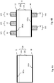
- FIG. 1 shows a first embodiment of the crystalline solar cell (1) according to the invention in a cross section.
- the solar cell (1) has a monocrystalline semiconductor material (10), for example made of silicon, in which a first region (101) and a second region (102) are formed each have such a doping that a pn junction is present between the first region (101) and the second region (102).
- the first region (101) is n-doped, has a sheet resistance in the range from 100 to 200 ⁇ ( ⁇ / ⁇ ) and serves as the emitter of the solar cell (1), while the second region (102) is p-doped is.
- the semiconductor material (10) has a first surface (101a), to which only the first area (101) of the semiconductor material (10) is adjacent and which is the front side (side facing the light) of the solar cell (1), and a second surface ( 102a), to which only the second region (102) of the semiconductor material (102) is adjacent and which is the rear side (the side facing away from the light) of the solar cell (1).
- the first surface (101a) is opposite the second surface (102a).
- the first surface (101a) can have a texture, ie a surface structure, according to the prior art, which improves the entry of the light into the semiconductor material (10). This texture is in the Fig. 1 not shown.
- the first region (101) of the semiconductor material was produced by introducing n-doping dopants, for example phosphorus (P), arsenic (As) or antimony (Sb), into the semiconductor material, for example by means of diffusion or ion implantation.
- n-doping dopants for example phosphorus (P), arsenic (As) or antimony (Sb)
- the first surface passivation layer (11) can be deposited on the first surface (101a) or produced by converting the semiconductor material (10), for example by oxidation.
- the surface passivation layer (11) covers in the in Fig. 1 the embodiment shown, the first surface (101a) of the semiconductor material over the entire lateral extent of the first surface (101a).
- the lateral expansion is the expansion in a plane perpendicular to the cross-sectional plane shown.
- first lateral areas (103) of the front side there is at least one front side contact (12), in the illustrated case three front side contacts (12), made of a first optically opaque, electrically conductive material, for example Ag, in first lateral areas (103) of the front side.
- the first surface passivation layer (11) is present between the front-side contact (12) and the first surface (101a) of the semiconductor material (10), so that an indirect, electrically conductive contact between the front-side contact (12) and the first area (101) of the Semiconductor material (10) consists.
- the first lateral regions (103) can have any shape in a plan view of the front side of the solar cell (1), ie in a plane perpendicular to the cross-sectional plane shown.
- the lateral areas (103) can be rectangular, straight stripes or winding stripes which extend into the plane of the drawing, or circular, elliptical, triangular or polygonal or freely shaped surfaces.
- the first lateral areas (103) can be arranged distributed regularly or irregularly over the entire front side of the solar cell (1).
- the thickness of the first optically nontransparent, electrically conductive material of the front-side contact (12) is in the range between 5 and 25 ⁇ m.
- the second lateral areas (104) of the front side of the solar cell (1) there is a layer (13) made of a first optically transparent, electrically conductive material, for example AlZnO (aluminum-doped zinc oxide), over the first surface passivation layer (11) and the first surface ( 101a) of the semiconductor material (10) arranged.
- a first optically transparent, electrically conductive material for example AlZnO (aluminum-doped zinc oxide)
- the second lateral areas (104) adjoin the first lateral areas (103) of the front side of the solar cell (1) and together with these form the entire front side of the solar cell (1).
- the second lateral regions (104) thus have a shape in the top view of the front side of the solar cell (1) which is complementary to the shape of the first lateral regions (103).
- the proportion of the first lateral areas (103) in the total area of the front side of the solar cell (1) in the top view is in the range from 1.5 to 3.0%.
- the layer (13) made of the first optically transparent, electrically conductive material has a thickness in the range from 10 to 50 nm, preferably 30 nm, and is in direct electrical contact with the front-side contact (12).
- the first surface passivation layer (11) is so thin with a thickness of 1 to 2 nm that charge carriers pass through it between the first region (101) of the semiconductor material (10) and the front-side contact (12) or the layer (13) from the first optically transparent, electrically conductive material can pass through.
- a first antireflection layer (14) is also arranged, which consists of silicon nitride (SiN) and has a thickness of 50 to 100 nm. This first anti-reflective layer (14) reduces the reflection of the light striking the solar cell (1) and improves the entry of the light into the solar cell (1).
- Characteristic of the solar cell (1) according to the invention in this and all other embodiments is that the layer (13) made of the first optically transparent, electrically conductive material, and preferably also the first anti-reflective layer (14), on the front side exclusively in the second lateral Areas (104) is formed and in the first lateral areas (103) is not present.
- the electrical contact of the front-side contact (s) (12) to the semiconductor material and the adhesion of the front-side contact (s) (12) are therefore essential compared to a structure in which an area of a less electrically conductive material, such as a transparent one, is between the front-side contact and the semiconductor material , electrically conductive oxide, is improved.
- the back of the solar cell (1) there is at least one back contact (16), in the illustrated case three back contacts (16), made of a second optically opaque, electrically conductive material, e.g. Al, in first lateral areas (105) of the back.
- the rear side contacts (16) directly adjoin the second surface (102a) of the semiconductor material (10) so that there is a direct, electrically conductive contact between the rear side contact (16) and the second area (102) of the semiconductor material (10).
- the first lateral areas (105) of the rear side can, as already described with reference to the first lateral areas (103) of the front side, have any shape in a plan view of the rear side of the solar cell (1) and can be arranged arbitrarily distributed over the entire rear side be.
- a 5 to 200 nm thick dielectric layer (15) is arranged on the second surface (102a) of the semiconductor material (10).
- the dielectric layer (15) consists, for example, of aluminum oxide, silicon oxide, silicon nitride or silicon oxynitride, or other materials suitable for the passivation and electrical insulation of p-type Si surfaces or a sequence of layers made of various of these materials. It electrically isolates the second surface (102a) of the semiconductor material (10) from a rear side connection (17) which connects the individual, local rear side contacts (16) to one another.
- the rear side connection (17) can consist of the same material as the rear side contacts (16) and can be applied together with them.
- the dielectric layer (15) consists of a 20 nm thin aluminum oxide layer (AlOx) and a 140 nm thick silicon nitride layer.
- the total thickness of the second, optically opaque, electrically conductive material of the rear-side contact (16) and the rear-side connection (17) is in the range between 3 and 30 ⁇ m, preferably 20 ⁇ m.
- the second lateral areas (106) adjoin the first lateral areas (105) of the rear side of the solar cell (1) and together with these form the entire rear side of the solar cell (1).
- the second lateral regions (106) thus have a shape in the top view of the rear side of the solar cell (1) which corresponds to the shape of the first lateral regions (105) is complementary.
- the proportion of the first lateral areas (105) in the total area of the rear side of the solar cell (1) in the top view is in the range from 1 to 5%.
- the shape and / or the dimensions and / or the lateral distribution and / or the proportion of the first lateral areas (105) of the rear side of the solar cell (1) can be identical to or different from the shape and / or the dimensions and / or the lateral Distribution and / or the proportion of the first lateral areas (103) of the front side of the solar cell (1) and be arranged independently of this distributed over the lateral extent of the rear side of the solar cell (1).
- the illustrated second embodiment of the crystalline solar cell (1) according to the invention differs from the first embodiment in that the solar cell (1) is a bifacial solar cell, the rear side of which is almost identical to the front side.
- the rear side instead of the dielectric layer, the rear side has a second surface passivation layer (18) and a layer (19) made of a second optically transparent, electrically conductive material in the second lateral regions (106).
- the second surface passivation layer (18) can be deposited on the second surface (102a) or produced by converting the semiconductor material (10), for example by oxidation.
- the second surface passivation layer (18) covers in the in Fig. 2 In the illustrated embodiment, the second surface (102a) of the semiconductor material over the entire lateral extent of the second surface (102a).
- the back of the solar cell (1) is at least one back contact (16), in the illustrated case two back contacts (16), made of a second optically nontransparent, electrically conductive material, for example Al, in first lateral areas (105) of the back arranged.
- the second surface passivation layer (18) is arranged between the back contact (16) and the second surface (102a) of the semiconductor material (10), so that an indirect, electrically conductive contact between the back contact (16) and the second area (102) of the Semiconductor material (10) is present.
- the layer (19) made of the second optically transparent, electrically conductive material for example ZnO (nitrogen-doped zinc oxide) or ITO (indium tin oxide), is arranged in the second lateral areas (106) of the rear side of the solar cell (1).
- the layer (19) made of the second optically transparent, electrically conductive material is in electrically conductive contact with the back contact (16) and via the second surface passivation layer (18) also to the second region (102) of the semiconductor material (10).
- the second surface passivation layer (18) in turn has a thickness in the range from 1 to 2 nm, so that charge carriers pass through it between the second region (102) of the semiconductor material (10) and the layer (19) made of the second optically transparent, electrically conductive Material can pass through.
- the layer (19) made of the second optically transparent, electrically conductive material is formed in the second lateral regions (106) with a thickness in the range from 10 to 50 nm.
- the thickness of the second, optically opaque, electrically conductive material of the rear-side contact (16) is in the range between 3 and 30 ⁇ m, preferably 20 ⁇ m.
- a second anti-reflection layer (20) is also arranged, which consists of silicon nitride or silicon oxynitride and has a thickness of 50 to 100 nm.
- the material and / or the thickness of the second antireflection layer (20) can be the same or different from the material and / or the thickness of the first antireflection layer (14).
- the second antireflection layer (20) reduces the reflection of the light incident on the rear side of the solar cell (1) and improves the entry of the light from the rear side into the solar cell (1).
- FIG. 3 a third embodiment of the solar cell (1) according to the invention is shown in cross section.
- the first region (101) of the semiconductor material (10) is n-doped and, adjacent to the first surface (101a), has a partial region (101b) which has an increased doping of the same type of doping as the remaining first region (101).
- the second region (102) is p-doped, has a sheet resistance in the range from 120 to 200 ⁇ ( ⁇ / ⁇ ) and serves as the emitter of the solar cell (n-PERL BJ).
- the first surface (101a) can have a texture, ie a surface structure, which improves the entry of light into the semiconductor material (10), this texture being in the Fig. 3 is not shown. If the total thickness of the semiconductor material (10) is greater than or equal to 10 ⁇ m, the partial area (101b) of the first area (101) has a thickness of 300 nm and the second area (102) has a thickness of 600 nm.
- first lateral areas (103) of the front side of the solar cell (1) there are at least one front side contact (12) in first lateral areas (103) of the front side of the solar cell (1), a layer (13) made of a first optically transparent, electrically conductive material and a first anti-reflective layer (14 ) as with reference to Fig. 1 described arranged.
- the embodiment shown consists in that the layer (19) made of a second optically transparent, electrically conductive material not only in the second lateral areas (106) of the rear side of the solar cell (1), but also in the first lateral areas (105) of the rear side the solar cell (1) is present.
- the second surface passivation layer (18) and the layer (19) made of the second optically transparent, electrically conductive material are thus arranged between the rear contact (16) and the second surface (102a) of the semiconductor material (10).
- the layer (19) made of the second optically transparent, electrically conductive material lies in the in Fig. 3 illustrated embodiment in the first lateral areas (105) with a smaller thickness than in the second lateral areas (106), but can also have the same thickness.
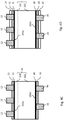
- FIG 4A a semiconductor material (10) is shown in which the first region (101) and the second region (102) are present. Any surface textures that have been formed are in the Figures 4A through 4F not shown.
- a first surface passivation layer (11) was produced over the whole area and a second surface passivation layer (18) was produced over the whole area on the second surface (102a) of the semiconductor material (10).
- These layers consist of silicon oxide and have a thickness of 1 to 2 nm. They were generated using rapid thermal oxidation, wet chemical oxidation or UV and ozone supported dry oxidation (SQi).
- front-side contacts (12) made of a first optically non-transparent, electrically conductive material are formed on the first surface (101a) and on the second surface (102a) of the semiconductor material (10) rear-side contacts (16) produced from a second optically opaque, electrically conductive material.
- the front and rear contacts (12, 16) are applied by screen printing in the first lateral areas (103, 105) of the respective surface (101a, 102a) and consist, for example, of a silver paste.
- the result of this process step is in Figure 4B shown.
- the first optically transparent, electrically conductive material and the second optically transparent, electrically conductive material is aluminum- or boron-doped zinc oxide, each of which is approximately 30 nm thick. The doping corresponds to the conductivity type of the semiconductor region (101, 102) adjoining the respective surface passivation layer (11, 18).
- Figure 4D shows the solar cell after a process step in which a first anti-reflective layer (14) on the layer (13) made of the first optically transparent, electrically conductive material and a second anti-reflective layer (20) on the layer (19) made of the second optically transparent, electrically conductive material were generated.
- the first anti-reflective layer (14) and the second anti-reflective layer (20) consist of silicon nitride and each have a thickness of approx. 60 nm.
- the layer (13) made of the first optically transparent, electrically conductive material, the layer (19) made of the second optically transparent, electrically conductive material, as well as the first anti-reflective layer (14) and the second anti-reflective layer (20) were in one and the same coating system generated in the order listed. However, different coating systems and other sequences of layer deposition are also possible, as long as the desired structure of the solar cell is implemented.
- the structure is made Figure 4D subjected to a temperature treatment.
- the solar cell is exposed to a temperature of 200 ° C to 300 ° C for approx. 1 min (one minute).
- lighting with white light with an intensity of at least 1000 W / m 2 can be made, whereby the parameters of the solar cell can be improved.
- the structure of the solar cell is not structurally changed by the temperature step. Only the first and / or the second optically opaque, electrically conductive material can diffuse into or through the respective first or second surface passivation layer (11 or 18). The result is a solar cell as shown in Fig. 2 is shown, wherein no firing of the contacts is necessary.
- Table 1 shows exemplary process parameters for a PECVD deposition of the layer made of the first and / or second optically transparent, electrically conductive material made of aluminum- or boron-doped zinc oxide. These relate to a PECVD system with a remote microwave plasma, in which the plasma space is spatially set back from the surface of a substrate to be coated, ie at a distance. This reduces the damage to the surface to be coated by ion bombardment from the plasma.
- parameter Area Preferred value Process pressure (chamber pressure) 0.1 - 0.2 mbar (10 - 20 Pa) 0.15 mbar (15 Pa)
- Process temperature (substrate temperature) 100 - 400 ° C 250 ° C Microwave plasma power 300-1000 W.
Landscapes
- Photovoltaic Devices (AREA)
- Life Sciences & Earth Sciences (AREA)
- Sustainable Development (AREA)
- Engineering & Computer Science (AREA)
- Sustainable Energy (AREA)
- Chemical & Material Sciences (AREA)
- Crystallography & Structural Chemistry (AREA)
- Physics & Mathematics (AREA)
- Plasma & Fusion (AREA)
Description
- Die Erfindung betrifft eine kristalline Solarzelle aus einem Halbleitermaterial, die auf der Vorderseite eine transparente, leitfähige Schicht zwischen den elektrischen Kontakten aufweist, sowie ein Verfahren zur Herstellung einer solchen Solarzelle.
- Herkömmliche Si-Solarzellen bestehen aus zwei entgegengesetzt dotierten Bereichen eines einkristallinen oder auch multikristallinen Halbleitermaterials. Dabei wird ein direkter pn-Übergang zwischen den beiden Bereichen durch das Einbringen von Dotanden in das Halbleitermaterial oder durch das Aufbringen einer Schicht aus dem gleichen Halbleitermaterial auf eine erste Schicht des Halbleitermaterials, wobei die zweite Schicht eine der Dotierung der ersten Schicht entgegengesetzte Dotierung aufweist, erzeugt. Eine solche Solarzelle wird auch Homo-Zelle im Gegensatz zu einer Hetero-Zelle, die aus unterschiedlichen Halbleitermaterialien besteht oder zwischen der n- und der p-Schicht noch eine intrinsische Schicht aufweist (pin-Übergang), genannt. Dabei wird bereits eine andere Struktur eines Halbleiters, bspw. amorph statt kristallin, als unterschiedliches Halbleitermaterial verstanden. Die entgegengesetzt dotierten Bereiche der Solarzelle werden elektrisch kontaktiert, wobei in vielen Solarzellen die Kontakte auf einander gegenüberliegenden Oberflächen des Halbleitermaterials, also auf der Vorderseite und der Rückseite der Solarzelle, angeordnet sind. Zur Verbesserung der Performance der Solarzelle werden die Oberflächen des Halbleitermaterials oftmals mit dielektrischen Schichten passiviert, wobei diese Passivierschichten auf der Vorderseite der Solarzelle, d.h. auf der der Lichtquelle zugewandten Seite, transparent sind und oft auch eine antireflektierende Wirkung haben oder durch eine Antireflektionsschicht ergänzt werden.
- Die elektrischen Kontakte werden zumindest auf der Vorderseite der Solarzelle nur lokal ausgebildet, um den Lichteinfall in das Halbleitermaterial durch das optisch intransparente elektrisch leitende Material, meist ein Metall, nur wenig zu behindern. Dazu wird das elektrisch leitende Material auf der Passivierungsschicht abgeschieden und der elektrische Kontakt anschließend durch Diffusion des elektrisch leitfähigen Materials durch die Passivierungsschicht bis zum Halbleitermaterial (Durchfeuern, Firing) erzeugt. Dabei entsteht ein direkter Kontakt zwischen dem elektrisch leitenden Material und dem Halbleitermaterial. Das Durchfeuern wird bei Temperaturen im Bereich von über 560°C bis 600°C ausgeführt.
- Die Rückseite der Solarzelle wird bei einigen Typen von Solarzellen (z.B. PERC-Zelle, Passivated Emitter Rear Contact) nur lokal kontaktiert, während die restlichen lateralen Abschnitte der Rückseite mit einer dielektrischen passivierenden Schicht versehen bleiben. Bei einigen Solarzellen ist die gesamte Rückseite mit einer passivierenden Schicht versehen und der elektrische Kontakt durch das Tunneln von Ladungsträgern durch diese Schicht realisiert (TOPCon-Zelle, Tunnel Oxide Passivated Contact). Diese Maßnahmen dienen der Reduzierung der Ladungsträgerrekombination an der Kontaktfläche zwischen elektrisch leitendem Material (Metall) und Halbleitermaterial.
- Um die Anzahl und Wirkung von Grenzflächenzuständen an der Oberfläche des Halbleitermaterials zu minimieren, wird der Emitter der Solarzelle, d.h. einer der beiden Halbleiterbereiche, weniger stark dotiert, wodurch jedoch die elektrische Leitfähigkeit dieses Bereiches sinkt. Bei einem hoch dotierten Emitter liegt der Flächenwiderstand im Bereich von 50 bis 100 Ω (Ω/□), während ein schwach dotierter Emitter einen Flächenwiderstand im Bereich von 100 bis 200 Ω (Ω/□) aufweist. Ein Ansatz zur Lösung dieses Problems ist die stärkere Dotierung nur eines kleinen lateralen Abschnitts des Emitters direkt unterhalb des elektrischen Kontaktes, so dass dieser Abschnitt einen Flächenwiderstand von ca. 60 Ω (Ω/□) aufweist.
- Ein anderer Ansatz, der in der
US 2010/0012179 A1 beschrieben ist, ist die ganzflächige Abscheidung eines elektrisch leitenden, optisch transparenten Materials, z.B. eines transparenten leitfähigen Oxids (TCO, transparent conducting oxide), auf dem Halbleitermaterial, gefolgt von einer Antireflektionsschicht, auf die ein Metall abgeschieden und anschließend durch die Antireflektionsschicht hindurchgefeuert wird. Die erhaltene Struktur ist dadurch gekennzeichnet, dass das Halbleitermaterial auf der Vorderseite der Solarzelle ganzflächig durch das elektrisch leitende, optisch transparente Material kontaktiert wird, welches wiederum elektrisch leitend mit den Metallkontakten verbunden ist. - Jedoch führt das Durchfeuern zu einer starken thermischen Belastung des Schichtstapels, wodurch es sowohl zu unerwünschten Effekten im Halbleitermaterial als auch zu einer Degradation des elektrisch leitenden, optisch transparenten Materials kommen kann, wodurch letztlich die Verbesserung der elektrische Kontaktierung des Halbleitermaterials sowie der Performance der Solarzelle wieder eingeschränkt wird. Darüber hinaus ist der Schritt zum Durchfeuern mit hohen Kosten und einem hohen Zeitaufwand verbunden. Des Weiteren wurden Probleme bezüglich der Haftung des Metalls auf dem elektrisch leitenden, optisch transparenten Material beobachtet, die zu einer Degradation der Langzeitstabilität und letztlich einem Ausfall der Solarzelle führen.
- Die
DE 38 31 857 A1 beschreibt eine Inversionsschicht-Solarzelle, bei der eine Raumladungszone im Halbleitermaterial durch die Erzeugung einer Verarmungszone an der Halbleiteroberfläche erreicht wird. Diese Verarmungszone ist durch ein auf der Halbleiteroberfläche aufgebrachtes Dielektrikum mit einer hohen positiven, ortsfesten Ladung bedingt. Das Dielektrikum kann aus Si, SiN, Mischformen oder anderen Dielektrika sowie Schichtstapeln daraus bestehen. Es ist eine hohe Ladungsdichte im Dielektrikum gewünscht, um eine hohe Inversionsladungsträgerdichte nahe der Halbleiteroberfläche zu erreichen. Das Dielektrikum erstreckt sich dabei zwischen den Metallkontakten auf der Vorderseite entlang der gesamten Halbleiteroberfläche, wobei es die Metallkontakte berührt, und ist optisch transparent. Zwischen dem Dielektrikum und der Halbleiteroberfläche ist ein Tunneloxid angeordnet. - Daher ist es Aufgabe der vorliegenden Erfindung, eine Solarzelle und ein Verfahren zur Herstellung einer solchen Solarzelle bereitzustellen, die die Nachteile des Standes der Technik verringern und insbesondere eine verbesserte Performance der Solarzelle und eine Reduzierung der Herstellungskosten ermöglicht.
- Diese Aufgabe wird gelöst durch eine kristalline Solarzelle gemäß Anspruch 1 und ein Verfahren gemäß Anspruch 11. Vorteilhafte Weiterbildungen und Ausführungsformen finden sich in den Unteransprüchen.
- Eine erfindungsgemäße kristalline Solarzelle weist einen ersten Bereich eines Halbleitermaterials mit einer ersten Dotierung, einen zweiten Bereich des Halbleitermaterials mit einer zweiten Dotierung, mindestens einen Vorderseitenkontakt aus einem ersten optisch intransparenten, elektrisch leitfähigen Material, der den ersten Bereich des Halbleitermaterials direkt oder indirekt in ersten lateralen Bereichen der Vorderseite der Solarzelle elektrisch leitend kontaktiert, und mindestens einen Rückseitenkontakt aus einem zweiten optisch intransparenten, elektrisch leitfähigen Material, der den zweiten Bereich des Halbleitermaterials direkt oder indirekt in ersten lateralen Bereichen der Rückseite der Solarzelle elektrisch leitend kontaktiert, auf. Mindestens über die Vorderseite der Solarzelle gelangt Licht bzw. eine elektromagnetische Strahlung in das Halbleitermaterial der Solarzelle. Die Vorder- und die Rückseite der Solarzelle sind einander gegenüberliegende Seiten oder Oberflächen der Solarzelle. Die erste Dotierung und die zweite Dotierung sind so gewählt, dass ein pn-Übergang zwischen dem ersten und dem zweiten Bereich vorliegt.
- Erfindungsgemäß ist auf der Vorderseite der Solarzelle ausschließlich in zweiten lateralen Bereichen eine Schicht aus einem ersten optisch transparenten, elektrisch leitfähigen Material über dem ersten Bereich des Halbleitermaterials angeordnet und mit dem mindestens einen Vorderseitenkontakt elektrisch leitend verbunden. Dabei ist zwischen der Schicht aus dem ersten optisch transparenten, elektrisch leitfähigen Material und dem ersten Bereich des Halbleitermaterials eine erste Oberflächenpassivierungsschicht angeordnet, durch die Ladungsträger hindurchtreten können. Damit steht die Schicht aus dem ersten optisch transparenten, elektrisch leitfähigen Material in indirektem, elektrisch leitendem Kontakt mit dem ersten Bereich des Halbleitermaterials. Die zweiten lateralen Bereiche der Vorderseite der Solarzelle sind von den ersten lateralen Bereichen der Vorderseite der Solarzelle verschieden. Die Oberflächenpassivierungsschicht, die vorzugsweise sehr dünn ausgebildet ist, verbessert die chemische Passivierung der Oberfläche des Halbleitermaterials und/oder reduziert die Anzahl und/oder Wirkung der Grenzflächenzustände an der Oberfläche des Halbleitermaterials.
- Im Sinne der Anmeldung wird unter einem direkten elektrisch leitenden Kontakt ein direkter physischer, ohmscher Kontakt zwischen zwei elektrisch leitenden Materialien oder Bereichen verstanden. Demgegenüber wird unter einem indirekten elektrisch leitenden Kontakt ein Kontakt verstanden, bei dem sich zwischen den beiden genannten elektrisch leitenden Materialien oder Bereichen ein weiteres Material oder ein weiterer Bereich befindet, das bzw. der entweder ebenfalls elektrisch leitend ist oder das bzw. der zwar dielektrisch, jedoch derart ausgestaltet ist, dass Ladungsträger durch dieses dielektrische Material bzw. Bereich hindurchtreten können. Insbesondere kann das dielektrische Material oder der dielektrische Bereich so dünn ausgebildet sein, dass Ladungsträger durch ihn hindurchtunneln können.
- Unter lateralen Bereichen einer Vorder- oder einer Rückseite der Solarzelle werden Bereiche der Solarzelle verstanden, die eine definierte Ausdehnung in einer Ebene der Vorder- bzw. der Rückseite der Solarzelle haben. In Dickenrichtung der Solarzelle, d.h. in einer Richtung, die Vorder- und Rückseite der Solarzelle senkrecht verbindet, erstrecken sich diese Bereiche jeweils von der Vorder- bzw. der Rückseite der Solarzelle bis zur jeweiligen Oberfläche des Halbleitermaterials. Die lateralen Bereiche können beliebige Formen in der Draufsicht auf die Vorder- bzw. die Rückseite haben, bspw. rund, eckig, linienförmig etc.
- Unter einem optisch transparenten Material wird ein Material verstanden, das Licht bzw. eine elektromagnetische Strahlung mit einer Wellenlänge, die von dem Halbleitermaterial der Solarzelle absorbiert wird, hindurchtreten lässt und kaum absorbiert oder reflektiert. Unter einem optisch intransparenten Material wird demgegenüber ein Material verstanden, das Licht bzw. eine elektromagnetische Strahlung mit einer Wellenlänge, die von dem Halbleitermaterial der Solarzelle absorbiert wird, absorbiert oder reflektiert und kaum hindurchtreten lässt.
- Die Schicht aus dem ersten optisch transparenten, elektrisch leitfähigen Material verbessert die Performance der Solarzelle, da sie Ladungsträger aus dem ersten Bereich des Halbleitermaterials in den zweiten lateralen Bereichen der Vorderseite der Solarzelle einsammelt und durch die höhere elektrische Leitfähigkeit in lateraler Richtung gegenüber dem ersten Bereich des Halbleitermaterials besser zu dem mindestens einen Vorderseitenkontakt abführt, als dies im Stand der Technik möglich ist.
- Vorzugsweise kommt als Halbleitermaterial Silizium, insbesondere einkristallines Silizium, zum Einsatz.
- Vorzugsweise ist die erste Oberflächenpassivierungsschicht auch zwischen dem mindestens einem Vorderseitenkontakt und dem ersten Bereich des Halbleitermaterials angeordnet.
- In einer bevorzugten Ausführungsform ist in zweiten lateralen Bereichen der Rückseite der Solarzelle eine Schicht aus einem elektrisch isolierenden Material über dem zweiten Bereich des Halbleitermaterials angeordnet, so dass der zweite Bereich des Halbleitermaterials in den zweiten lateralen Bereichen elektrisch isoliert ist, insbesondere gegenüber einer elektrischen Verbindungsleitung, die den mindestens einen Rückseitenkontakt mit einem elektrischen Anschluss außerhalb der Solarzelle verbindet. Die zweiten lateralen Bereiche der Rückseite der Solarzelle sind von den ersten lateralen Bereichen der Rückseite der Solarzelle verschieden.
- In einer anderen bevorzugten Ausführungsform ist in zweiten lateralen Bereichen der Rückseite der Solarzelle eine Schicht aus einem zweiten optisch transparenten, elektrisch leitfähigen Material über dem ersten Bereich des Halbleitermaterials angeordnet und mit dem mindestens einen Rückseitenkontakt elektrisch leitend verbunden. Dabei steht die Schicht aus dem zweiten optisch transparenten, elektrisch leitfähigen Material in direktem oder indirektem, elektrisch leitendem Kontakt mit dem zweiten Bereich des Halbleitermaterials. Die zweiten lateralen Bereiche der Rückseite der Solarzelle sind von den ersten lateralen Bereichen der Rückseite der Solarzelle verschieden.
- In der zuletzt beschriebenen Ausführungsform ist das zweite optisch transparente, elektrisch leitfähige Material vorzugsweise auch zwischen dem zweiten Bereich des Halbleitermaterials und dem Rückseitenkontakt, also auch in den ersten lateralen Bereichen der Rückseite der Solarzelle, angeordnet.
- Analog wie mit Bezug auf die Vorderseite der Solarzelle beschrieben, ist vorzugsweise zwischen der Schicht aus dem zweiten optisch transparenten, elektrisch leitfähigen Material und dem zweiten Bereich des Halbleitermaterials und/oder zwischen dem Rückseitenkontakt und dem zweiten Bereich des Halbleitermaterials eine zweite Oberflächenpassivierungsschicht angeordnet, durch die Ladungsträger hindurchtreten können. Auch hier ergeben sich die oben beschriebenen Vorteile.
- Die Ausführungsformen, bei denen auch auf der Rückseite der Solarzelle ein optisch transparentes, elektrisch leitfähiges Material angeordnet ist, sind besonders vorteilhaft für bifaciale (bifaziale) Solarzellen, bei denen Licht sowohl von der Vorder- als auch der Rückseite in das Halbleitermaterial einstrahlen kann.
- Vorzugsweise sind das erste und gegebenenfalls das zweite optisch transparente, elektrisch leitfähige Material aus der Gruppe bestehend aus Indium-Zinn-oxid, Fluor-Zinn-Oxid, Aluminium- und/oder Bor-dotiertes -Zink-Oxid und Antimon-Zinn-Oxid ausgewählt. Das erste und gegebenenfalls das zweite optisch transparente, elektrisch leitfähige Material weisen dabei eine elektrische Leifähigkeit im Bereich von 2·103 bis 100·101 S/m bzw. einen spezifischen Widerstand im Bereich von 1 · 10-4 bis 50·10-4 Qcm (Flächenwiderstand < 10 Ω/□) auf.
- Vorzugsweise hat die Schicht aus dem ersten optisch transparenten, elektrisch leitfähigen Material und/oder die Schicht aus dem zweiten optisch transparenten, elektrisch leitfähigen Material eine Dicke im Bereich von 10 bis 100 nm, besonders bevorzugt im Bereich von 10 bis 50 nm. Für den Fall, dass die Schicht aus dem zweiten optisch transparenten, elektrisch leitfähigen Material auch zwischen dem mindestens einen Rückseitenkontakt und dem Halbleitermaterial angeordnet ist, kann die Dicke dieser Schicht in den ersten lateralen Bereichen der Rückseite der Solarzeile auch verringert sein und bspw. nur größer oder gleich 10 % der Dicke der Schicht in den zweiten lateralen Bereichen der Rückseite der Solarzeile betragen.
- Die Schicht aus dem ersten optisch transparenten, elektrisch leitfähigen Material und die Schicht aus dem zweiten optisch transparenten, elektrisch leitfähigen Material können aus demselben oder aus unterschiedlichen Materialien bestehen und die gleiche oder unterschiedliche Dicken aufweisen.
- Das erste und das zweite optisch intransparente, elektrisch leitfähige Material sind vorzugsweise aus der Gruppe bestehend aus Aluminium, Silber, Kupfer, Nickel, Vanadium und Kombinationen und Legierungen der Selbigen ausgewählt, wobei dies dasselbe Material oder unterschiedliche Materialien sein können. Das erste und das zweite optisch intransparente, elektrisch leitfähige Material zeichnen sich durch eine hohe elektrische Leitfähigkeit, eine große Langzeitstabilität und die Eignung zur Verbindung mit anderen Baugruppen, z.B. eines Solarmoduls, aus.
- Vorzugsweise weisen die erste und/oder die zweite Oberflächenpassivierungsschicht eine Dicke im Bereich von 1 bis 20 nm auf und bestehen aus einem Material, das aus der Gruppe bestehend aus Siliziumoxid, Siliziumnitrid, Siliziumoxynitrid und Aluminiumoxid ausgewählt ist. Das Material und/oder die Dicke der ersten und der zweiten Oberflächenpassivierungsschicht können gleich oder verschieden voneinander sein.
- Der erste Bereich des Halbleitermaterials ist vorzugsweise n-leitend dotiert und ist der Emitter der Solarzelle mit einem elektrischen Flächenwiderstand im Bereich von 100 bis 200 Ω (Ω/□). In diesem Fall ist der zweite Bereich des Halbleitermaterials p-dotiert und bildet die Basis (bulk) der Solarzelle.
- In einer anderen Ausführungsform ist der erste Bereich des Halbleitermaterials n-dotiert und bildet die Basis (bulk) der Solarzelle, während der zweite Bereich des Halbleitermaterials p-dotiert ist und den Emitter der Solarzelle bildet und einen elektrischen Flächenwiderstand im Bereich von 120 bis 200 Ω (Ω/□) aufweist. In dieser Ausführungsform ist die Anordnung des zweiten optisch transparenten, elektrisch leitfähigen Materials in den zweiten lateralen Bereichen der Rückseite der Solarzelle oder in den ersten und den zweiten lateralen Bereichen der Rückseite der Solarzelle, wie oben beschrieben, von besonderem Vorteil.
- Das erfindungsgemäße Verfahren zur Herstellung einer erfindungsgemäßen kristallinen Solarzelle weist die Schritte zum Bereitstellen eines Halbleitermaterials mit einem ersten Bereich und einem zweiten Bereich, zum Erzeugen einer ersten Oberflächenpassivierungsschicht, durch die Ladungsträger hindurchtreten können, auf oder an einer ersten Oberfläche des Halbleitermaterials, zum Aufbringen eines ersten optisch intransparenten, elektrisch leitfähigen Materials auf der ersten Oberflächenpassivierungsschicht in ersten lateralen Bereichen der ersten Oberfläche des Halbleitermaterials und zum Erzeugen mindestens eines direkten oder indirekten elektrisch leitenden Kontaktes zwischen dem ersten optisch intransparenten, elektrisch leitfähigen Material und dem ersten Bereich des Halbleitermaterials in den ersten lateralen Bereichen der ersten Oberfläche des Halbleitermaterials, zum Aufbringen einer Schicht aus einem ersten optisch transparenten, elektrisch leitfähigem Material auf der ersten Oberflächenpassivierungsschicht in zweiten lateralen Bereichen der ersten Oberfläche des Halbleitermaterials und zum Aufbringen eines zweiten optisch intransparenten, elektrisch leitfähigen Materials in ersten lateralen Bereichen einer zweiten Oberfläche des Halbleitermaterials und zum Erzeugen mindestens eines direkten oder indirekten elektrisch leitenden Kontaktes zwischen dem zweiten optisch intransparenten, elektrisch leitfähigen Material und dem zweiten Bereich des Halbleitermaterials in den ersten lateralen Bereichen der zweiten Oberfläche des Halbleitermaterials auf. Dabei sind der erste Bereich und der zweite Bereich des Halbleitermaterials so dotiert, dass ein pn-Übergang zwischen dem ersten Bereich und dem zweiten Bereich vorliegt. Die erste Oberfläche ist dadurch gekennzeichnet, dass nur der erste Bereich des Halbleitermaterials an sie angrenzt, und stellt die, auf jeden Fall einer Lichtquelle zugewandte Seite der herzustellenden Solarzelle, d.h. die Vorderseite, dar. Die zweite Oberfläche ist dadurch gekennzeichnet, dass nur der zweite Bereich des Halbleitermaterials an sie angrenzt, und stellt die, einer Lichtquelle abgewandte Seite der herzustellenden Solarzelle, d.h. die Rückseite, dar. Damit liegt die zweite Oberfläche des Halbleitermaterials der ersten Oberfläche des Halbleitermaterials gegenüber.
- Im Laufe des Verfahrens, vorzugsweise während des Schrittes zum Aufbringen der Schicht aus dem ersten optisch transparenten, elektrisch leitfähigen Material, wird ein elektrisch leitender Kontakt zwischen dieser Schicht und dem ersten optisch intransparenten, elektrisch leitfähigen Material sowie ein elektrisch leitender Kontakt zwischen der Schicht aus dem ersten optisch transparenten, elektrisch leitfähigen Material und dem ersten Bereich des Halbleitermaterials erzeugt.
- Der Schritt zum Aufbringen des ersten optisch transparenten, elektrisch leitfähigen Materials wird erfindungsgemäß nach dem Schritt zum Aufbringen des ersten optisch intransparenten, elektrisch leitfähigen Materials, d.h. nach der Abscheidung des Materials des mindestens eines Vorderseitenkontaktes, ausgeführt. Der Schritt zum Aufbringen eines zweiten optisch intransparenten, elektrisch leitfähigen Materials in die ersten lateralen Bereiche einer zweiten Oberfläche des Halbleitermaterials und zum Erzeugen des mindestens eines direkten oder indirekten elektrisch leitenden Kontaktes zwischen dem zweiten optisch intransparenten, elektrisch leitfähigen Material und dem zweiten Bereich des Halbleitermaterials, d.h. die Herstellung mindestens eines Rückseitenkontaktes, kann vor oder nach oder zwischen den Schritten zum Abscheiden und Herstellen des Vorderseitenkontaktes und zum Aufbringen der Schicht aus dem ersten optisch transparenten, elektrisch leitfähigen Material ausgeführt werden. Vorzugsweise wird der zum Aufbringen eines zweiten optisch intransparenten, elektrisch leitfähigen Materials vor oder zwischen den Schritten zum Abscheiden und Herstellen des Vorderseitenkontaktes und zum Aufbringen der Schicht aus dem ersten optisch transparenten, elektrisch leitfähigen Material ausgeführt.
- Optional wird nach dem Aufbringen des ersten optisch intransparenten, elektrisch leitfähigen Materials eine Temperaturbehandlung ausgeführt. Die Temperaturbehandlung bewirkt eine Diffusion des ersten optisch intransparenten, elektrisch leitfähigen Materials in oder durch die darunterliegende erste Oberflächenpassivierungsschicht und stellt damit den direkten elektrisch leitenden Kontakt zum ersten Bereich des Halbleitermaterials her oder verbessert den indirekten elektrisch leitenden Kontakt zum ersten Bereich des Halbleitermaterials. Diese Temperaturbehandlung wird jedoch im Gegensatz zum Durchfeuern oder Firing bei niedrigeren Temperaturen von ca. 200 bis 560°C ausgeführt. Die Temperaturbehandlung erfolgt vorzugsweise nach dem Aufbringen der Schicht aus dem ersten optisch transparenten, elektrisch leitfähigen Material und besonders bevorzugt auch nach einem Schritt zum Aufbringen einer Antireflektionsschicht über der Schicht aus dem ersten optisch transparenten, elektrisch leitfähigen Material und kann eine Beleuchtung des gesamten Schichtaufbaus mit normalem (weißem) Licht (z.B. einer Halogenlampe) mit einer Stärke von größer als oder gleich 1000 W/m2 für einige Sekunden (≥ 10 s) bis einigen Minuten einschließen. Besonders bevorzugt erfolgt die Temperaturbehandlung erst nach dem Aufbringen aller funktionalen Schichten der Solarzelle, d.h. nach dem Aufbringen des ersten und des zweiten optisch intransparenten, elektrisch leitfähigen Materials, des ersten und ggf. eines zweiten optisch transparenten, elektrisch leitfähigen Materials, ggf. eines elektrisch isolierenden Materials und einer ersten und ggf. einer zweiten Antireflektionsschicht.
- In einer Ausführungsform des Verfahrens wird vor oder nach dem Schritt zum Aufbringen des zweiten optisch intransparenten, elektrisch leitfähigen Materials in den ersten lateralen Bereichen der zweiten Oberfläche des Halbleitermaterials eine Schicht aus einem elektrisch isolierenden Material über der zweiten Oberfläche des Halbleitermaterials in zweiten lateralen Bereichen der zweiten Oberfläche des Halbleitermaterials aufgebracht. Damit wird der zweite Bereich des Halbleitermaterials in den zweiten lateralen Bereichen elektrisch isoliert, so dass eine Solarzelle mit passivierter Rückseite erzeugt wird. Die zweiten lateralen Bereiche der zweiten Oberfläche des Halbleitermaterials sind von den ersten lateralen Bereichen der zweiten Oberfläche des Halbleitermaterials verschieden. Wird das elektrisch isolierende Material vor dem Schritt zum Aufbringen des zweiten optisch intransparenten, elektrisch leitfähigen Materials aufgebracht, so kann das elektrisch isolierende Material ganzflächig auf der zweiten Oberfläche des Halbleitermaterials ausgebildet werden. Im Anschluss wird das elektrisch isolierende Material aus den ersten lateralen Bereichen der zweiten Oberfläche des Halbleitermaterials wieder entfernt.
- In einer anderen Ausführungsform des Verfahrens wird vor oder nach dem Schritt zum Aufbringen des zweiten optisch intransparenten, elektrisch leitfähigen Materials in den ersten lateralen Bereichen der zweiten Oberfläche des Halbleitermaterials eine Schicht aus einem zweiten optisch transparenten, elektrisch leitfähigen Material in zweiten lateralen Bereichen der zweiten Oberfläche des Halbleitermaterials aufgebracht. Dabei sind die zweiten lateralen Bereiche der zweiten Oberfläche von den ersten lateralen Bereichen der zweiten Oberfläche verschieden. Letztlich wird ein elektrisch leitender Kontakt zwischen der Schicht aus dem zweiten optisch transparenten, elektrisch leitfähigen Material und dem zweiten optisch intransparenten, elektrisch leitfähigen Material sowie zwischen der Schicht aus dem zweiten optisch transparenten, elektrisch leitfähigen Material und dem zweiten Bereich des Halbleitermaterials erzeugt. Bei der Herstellung des Rückseitenkontaktes ist dabei die Ausführungsform, wie sie bezüglich der Herstellung des Vorderseitenkontaktes beschrieben wurde, möglich. Das heißt, zunächst kann das zweite optisch intransparente, elektrisch leitfähige Material in den ersten lateralen Bereichen der zweiten Oberfläche des Halbleitermaterials aufgebracht und danach die Schicht aus dem zweiten optisch transparenten, elektrisch leitfähigen Material in den zweiten lateralen Bereichen der zweiten Oberfläche des Halbleitermaterials aufgebracht werden. Jedoch ist auch eine Ausführungsform, bei der zuerst die Schicht aus dem zweiten optisch transparenten, elektrisch leitfähigen Material ganzflächig über der zweiten Oberfläche des Halbleitermaterials und anschließend das zweite optisch intransparente, elektrisch leitfähige Material in den ersten lateralen Bereichen der zweiten Oberfläche des Halbleitermaterials aufgebracht wird, möglich. Dabei kann der Kontakt des zweiten optisch intransparenten, elektrisch leitfähigen Materials zum zweiten Bereich des Halbleitermaterials erzeugt werden, wie dies mit Bezug auf die Herstellung einer Solarzelle mit passivierter Rückseite beschrieben wurde.
- Vorzugsweise wird vor dem Schritt zum Aufbringen des zweiten optisch intransparenten, elektrisch leitfähigen Materials und vor dem Schritt zum Aufbringen der Schicht aus dem zweiten optisch transparenten, elektrisch leitfähigen Material eine zweite Oberflächenpassivierungsschicht, durch die Ladungsträger hindurchtreten können, auf oder an der zweiten Oberfläche des Halbleitermaterials erzeugt.
- In einer bevorzugten Ausführungsform wird über der Schicht aus dem ersten optisch transparenten, elektrisch leitfähigen Material eine erste Antireflektionsschicht und/oder gegebenenfalls über der Schicht aus dem zweiten optisch transparenten, elektrisch leitfähigen Material eine zweite Antireflektionsschicht aufgebracht. Zumindest die erste Antireflektionsschicht wird somit nach dem Aufbringen des ersten optisch intransparenten, elektrisch leitfähigen Materials aufgebracht.
- Vorzugsweise werden die Schicht aus dem ersten optisch transparenten, elektrisch leitfähigen Material und die erste Antireflektionsschicht und/oder gegebenenfalls die Schicht aus dem zweiten optisch transparenten, elektrisch leitfähigen Material und die zweite Antireflektionsschicht jeweils in einer Anlage und ohne Unterbrechung eines Vakuums aufgebracht. Damit kann eine Feuchtigkeitsaufnahme der Schicht aus dem ersten optisch transparenten, elektrisch leitfähigen Material bzw. der Schicht aus dem zweiten optisch transparenten, elektrisch leitfähigen Material während einer Vakuumunterbrechung vermieden und damit die jeweilige Schicht vor Korrosion geschützt und die Langzeitstabilität ihrer Parameter verbessert werden.
- Die Schicht aus dem ersten optisch transparenten, elektrisch leitfähigen Material und/oder die Schicht aus dem zweiten optisch transparenten, elektrisch leitfähigen Material werden vorzugsweise mittels eines PECVD-Prozesses (Plasmaunterstützte chemische Gasphasenabscheidung, Plasma Enhanced Chemical Vapour Deposition), bei dem ein Plasma in einer Plasmazone vorliegt, abgeschieden. Dabei sind Prozesse, die eine geringe Oberflächenschädigung des Halbleitermaterials bewirken, besonders bevorzugt. Solche Prozesse sind beispielsweise Plasmaprozesse, bei denen das Plasma durch Mikrowellen angeregt wird und/oder bei denen die Plasmazone von der jeweiligen zu beschichtenden Oberfläche des Halbleitermaterials räumlich zurückgesetzt ist. Dies ermöglicht eine sehr schonende Abscheidung des optisch transparenten, elektrisch leitfähigen Materials, ohne die jeweilige Oberfläche des Halbleitermaterials durch das Auftreffen von hochenergetischen Ionen zu stören. Darüber hinaus bietet das Abscheiden dieser Schichten mittels PECVD-Prozess den Vorteil, dass das jeweilige optisch transparente, elektrisch leitfähige Material sowie die jeweilige Antireflektionsschicht auf dem jeweiligen optisch intransparenten, elektrisch leitfähigen Material schlecht aufwächst (selektiver Prozess). Damit kann das optisch transparente, elektrisch leitfähige Material, welches den mindestens einen Vorderseitenkontakt oder den mindestens einen Rückseitenkontakt der hergestellten Solarzelle bildet, einfach und ohne kompliziertes Entfernen von überlagerten Schichten direkt von außen elektrisch kontaktiert werden. Vorzugsweise wird die zu beschichtende Oberfläche (101a, 102a) des Halbleitermaterials (10) während des Abscheideprozesses linear an der Plasmazone vorbeibewegt.
- Vorzugsweise sind das erste und/oder das zweite optisch transparente, elektrisch leitfähige Material ein Zinkoxid, das besonders bevorzugt mit Aluminium oder Bor dotiert ist. Das bevorzugte Abscheideverfahren für dieses Material ist ein Mikrowellen-gestützter PECVD-Prozess mit den Ausgangsstoffen Diethylzink (DEtZ oder DEZ) oder Dimethylzink (DMZ) als Zinklieferant, Distickstoffmonoxid (N2O, Lachgas) und/oder Sauerstoff (O2) als Sauerstofflieferant sowie einem Inertgas (Argon, Neon oder Helium) und/oder Stickstoff. Für die Abscheidung eines Aluminium-dotierten Zinkoxids wird darüber hinaus vorzugsweise Trimethylaluminium (TMAI oder TMA) als Aluminiumquelle und für die Abscheidung eines Bor-dotierten Zinkoxids vorzugsweise Diboran (B2H6) als Borquelle hinzugefügt.
- Im Nachfolgenden soll die Erfindung anhand von Ausführungsbeispielen und Figuren verdeutlicht werden, wobei gleichartige Elemente, Schichten oder Bereiche mit gleichen Bezugszeichen gekennzeichnet, Größen- und Dickenverhältnisse jedoch nicht maßstabsgerecht dargestellt sind.
- Es zeigen:
- Fig. 1
- eine erste Ausführungsform der erfindungsgemäßen Solarzelle (1) mit einer passivierten Rückseite;
- Fig. 2
- eine zweite Ausführungsform der erfindungsgemäßen Solarzelle (1) mit einer Schicht (19) aus einem zweiten optisch transparenten, elektrisch leitfähigen Material auf der Rückseite, wobei die Schicht (19) aus dem zweiten optisch transparenten, elektrisch leitfähigen Material nur in zweiten lateralen Bereichen (106) der Rückseite angeordnet ist;
- Fig. 3
- eine dritte Ausführungsform der erfindungsgemäßen Solarzelle (1) mit einer Schicht (19) aus einem zweiten optisch transparenten, elektrisch leitfähigen Material auf der Rückseite, wobei die Schicht (19) aus dem zweiten optisch transparenten, elektrisch leitfähigen Material auch in ersten lateralen Bereichen (105) der Rückseite angeordnet ist; und
- Fig. 4A bis 4D
- eine beispielhafte Ausführungsform des erfindungsgemäßen Verfahrens anhand von Querschnitten durch die Solarzelle in unterschiedlichen Verfahrensstadien.
-
Figur 1 zeigt eine erste Ausführungsform der erfindungsgemäßen kristallinen Solarzelle (1) in einem Querschnitt. Die Solarzelle (1) weist ein einkristallines Halbleitermaterial (10), bspw. aus Silizium, auf, in dem ein erster Bereich (101) und ein zweiter Bereich (102) ausgebildet sind, die jeweils eine derartige Dotierung aufweisen, dass ein pn-Übergang zwischen dem ersten Bereich (101) und dem zweiten Bereich (102) vorliegt. Im vorliegenden Fall ist der erste Bereich (101) n-dotiert, weist einen Flächenwiderstand im Bereich von 100 bis 200 Ω (Ω/□) auf und dient als Emitter der Solarzelle (1), während der zweite Bereich (102) p-dotiert ist. Das Halbleitermaterial (10) hat eine erste Oberfläche (101a), an die nur der erste Bereich (101) des Halbleitermaterials (10) angrenzt und die die Vorderseite (dem Licht zugewandte Seite) der Solarzelle (1) ist, und eine zweite Oberfläche (102a), an die nur der zweite Bereich (102) des Halbleitermaterials (102) angrenzt und die die Rückseite (die dem Licht abgewandte Seite) der Solarzelle (1) ist. Die erste Oberfläche (101a) liegt der zweiten Oberfläche (102a) gegenüber. Die erste Oberfläche (101a) kann eine Textur, d.h. eine Oberflächenstruktur, gemäß dem Stand der Technik aufweisen, die den Eintritt des Lichtes in das Halbleitermaterial (10) verbessert. Diese Textur ist in derFig. 1 nicht dargestellt. Der erste Bereich (101) des Halbleitermaterials wurde durch das Einbringen von n-dotierenden Dotanden, bspw. Phosphor (P), Arsen (As) oder Antimon (Sb), in das Halbleitermaterial, bspw. mittels Diffusion oder Ionenimplantation, erzeugt. - Auf oder an der ersten Oberfläche (101a) des Halbleitermaterials (10) ist eine erste Oberflächenpassivierungsschicht (11), bspw. aus SiO2 oder SiON, angeordnet. Die erste Oberflächenpassivierungsschicht (11) kann auf der ersten Oberfläche (101a) abgeschieden oder durch eine Umwandlung des Halbleitermaterials (10), bspw. durch Oxidation, erzeugt werden. Die Oberflächenpassivierungsschicht (11) bedeckt dabei in der in
Fig. 1 dargestellten Ausführungsform die erste Oberfläche (101a) des Halbleitermaterials über die gesamte laterale Ausdehnung der ersten Oberfläche (101a). Die laterale Ausdehnung ist die Ausdehnung in einer Ebene senkrecht zur dargestellten Querschnittsebene. - Auf der Vorderseite der Solarzelle (1) ist mindestens ein Vorderseitenkontakt (12), im dargestellten Fall drei Vorderseitenkontakte (12), aus einem ersten optisch intransparenten, elektrisch leitfähigen Material, bspw. Ag, in ersten lateralen Bereichen (103) der Vorderseite angeordnet. Die erste Oberflächenpassivierungsschicht (11) liegt dabei zwischen dem Vorderseitenkontakt (12) und der ersten Oberfläche (101a) des Halbleitermaterials (10) vor, so dass ein indirekter, elektrisch leitender Kontakt zwischen dem Vorderseitenkontakt (12) und dem ersten Bereich (101) des Halbleitermaterials (10) besteht. Die ersten lateralen Bereiche (103) können eine beliebige Form in einer Draufsicht auf die Vorderseite der Solarzelle (1), d.h. in einer Ebene senkrecht zur dargestellten Querschnittsebene, aufweisen. Insbesondere können die lateralen Bereiche (103) rechteckige, geradlinig verlaufende Streifen oder gewundene Streifen, die sich in die Zeichnungsebene hinein erstrecken, oder kreisförmige, elliptische, drei- oder mehreckige oder frei geformte Flächen sein. Dabei können die ersten lateralen Bereiche (103) regelmäßig oder unregelmäßig über die gesamte Vorderseite der Solarzelle (1) verteilt angeordnet sein. Die Dicke des ersten optisch intransparenten, elektrisch leitenden Materials des Vorderseitenkontakts (12) liegt im Bereich zwischen 5 bis 25 µm.
- In zweiten lateralen Bereichen (104) der Vorderseite der Solarzelle (1) ist eine Schicht (13) aus einem ersten optisch transparenten, elektrisch leitfähigen Material, bspw. AlZnO (Aluminiumdotiertes Zinkoxid), über der ersten Oberflächenpassivierungsschicht (11) und der ersten Oberfläche (101a) des Halbleitermaterials (10) angeordnet. Daher liegt ein indirekter, elektrisch leitender Kontakt zwischen der Schicht (13) aus dem ersten optisch transparenten, elektrisch leitfähigen Material und dem ersten Bereich (101) des Halbleitermaterials (10) vor. Die zweiten lateralen Bereiche (104) grenzen an die ersten lateralen Bereiche (103) der Vorderseite der Solarzelle (1) an und bilden gemeinsam mit diesen die gesamte Vorderseite der Solarzelle (1) ab. Damit weisen die zweiten lateralen Bereiche (104) eine Form in der Draufsicht auf die Vorderseite der Solarzelle (1) auf, die zu der Form der ersten lateralen Bereiche (103) komplementär ist. Der Anteil der ersten lateralen Bereiche (103) an der gesamten Fläche der Vorderseite der Solarzelle (1) in der Draufsicht liegt im Bereich von 1,5 bis 3,0 %.
- Die Schicht (13) aus dem ersten optisch transparenten, elektrisch leitfähigen Material weist eine Dicke im Bereich von 10 bis 50 nm, vorzugsweise von 30 nm, auf und steht in direktem elektrischen Kontakt mit dem Vorderseitenkontakt (12).
- Die erste Oberflächenpassivierungsschicht (11) ist mit einer Dicke von 1 bis 2 nm so dünn, dass Ladungsträger durch sie zwischen dem ersten Bereich (101) des Halbleitermaterials (10) und dem Vorderseitenkontakt (12) bzw. der Schicht (13) aus dem ersten optisch transparenten, elektrisch leitfähigen Material hindurchtreten können.
- In den zweiten lateralen Bereichen (104) der Vorderseite der Solarzelle (1) ist des Weiteren eine erste Antireflektionschicht (14) angeordnet, die aus Siliziumnitrid (SiN) besteht und eine Dicke von 50 bis 100 nm aufweist. Diese erste Antireflektionsschicht (14) verringert die Reflexion des auf die Solarzelle (1) auftreffenden Lichtes und verbessert den Eintritt des Lichtes in die Solarzelle (1).
- Kennzeichnend für die erfindungsgemäße Solarzelle (1) in dieser und allen anderen Ausführungsformen ist, dass die Schicht (13) aus dem ersten optisch transparenten, elektrisch leitfähigen Material, und vorzugsweise auch die erste Antireflektionsschicht (14), auf der Vorderseite ausschließlich in den zweiten lateralen Bereichen (104) ausgebildet ist und in den ersten lateralen Bereichen (103) nicht vorliegt. Damit ist der elektrische Kontakt des oder der Vorderseitenkontakte (12) zum Halbleitermaterial und die Haftung des oder der Vorderseitenkontakte (12) wesentlich gegenüber einem Aufbau, in dem zwischen dem Vorderseitenkontakt und dem Halbleitermaterial ein Bereich eines elektrisch schlechter leitenden Materials, wie bspw. eines transparenten, elektrisch leitenden Oxids, vorliegt, verbessert.
- Auf der Rückseite der Solarzelle (1) ist mindestens ein Rückseitenkontakt (16), im dargestellten Fall drei Rückseitenkontakte (16), aus einem zweiten optisch intransparenten, elektrisch leitfähigen Material, bspw. Al, in ersten lateralen Bereichen (105) der Rückseite angeordnet. Die Rückseitenkontakte (16) grenzen direkt an die zweite Oberfläche (102a) des Halbleitermaterials (10) an, so dass ein direkter, elektrisch leitender Kontakt zwischen dem Rückseitenkontakt (16) und dem zweiten Bereich (102) des Halbleitermaterials (10) vorliegt. Die ersten lateralen Bereiche (105) der Rückseite können, wie bereits mit Bezug auf die ersten lateralen Bereiche (103) der Vorderseite beschrieben, eine beliebige Form in einer Draufsicht auf die Rückseite der Solarzelle (1) aufweisen und beliebig über die gesamte Rückseite verteilt angeordnet sein.
- In zweiten lateralen Bereichen (106) der Rückseite der Solarzelle (1) ist eine 5 bis 200 nm dicke dielektrische Schicht (15) an der zweiten Oberfläche (102a) des Halbleitermaterials (10) angeordnet. Die dielektrische Schicht (15) besteht bspw. aus Aluminiumoxid, Siliziumoxid, Siliziumnitrid oder Siliziumoxynitrid, oder anderen für die Passivierung und elektrische Isolierung von p-type Si-Oberflächen geeigneten Materialien oder einer Sequenz aus Schichten aus verschiedenen dieser Materialien. Sie isoliert die zweite Oberfläche (102a) des Halbleitermaterials (10) elektrisch von einer Rückseitenverbindung (17), die die einzelnen, lokalen Rückseitenkontakte (16) miteinander verbindet. Die Rückseitenverbindung (17) kann aus demselben Material wie die Rückseitenkontakte (16) bestehen und mit diesen zusammen aufgebracht werden. Beispielhaft besteht die dielektrische Schicht (15) aus einer 20 nm dünnen Aluminiumoxid-Schicht (AlOx) und einer 140 nm dicken Siliziumnitridschicht. Die Gesamtdicke des zweiten optisch intransparenten, elektrisch leitfähigen Materials des Rückseitenkontakts (16) und der Rückseitenverbindung (17) liegt im Bereich zwischen 3 bis 30 µm, vorzugweise bei 20 µm.
- Die zweiten lateralen Bereiche (106) grenzen an die ersten lateralen Bereiche (105) der Rückseite der Solarzelle (1) an und bilden gemeinsam mit diesen die gesamte Rückseite der Solarzelle (1) ab. Damit weisen die zweiten lateralen Bereiche (106) eine Form in der Draufsicht auf die Rückseite der Solarzelle (1) auf, die zu der Form der ersten lateralen Bereiche (105) komplementär ist. Der Anteil der ersten lateralen Bereiche (105) an der gesamten Fläche der Rückseite der Solarzelle (1) in der Draufsicht liegt im Bereich von 1 bis 5 %. Dabei können die Form und/oder die Abmessungen und/oder die laterale Verteilung und/oder der Anteil der ersten lateralen Bereiche (105) der Rückseite der Solarzelle (1) gleich oder verschieden zu der Form und/oder den Abmessungen und/oder der lateralen Verteilung und/oder dem Anteil der ersten lateralen Bereiche (103) der Vorderseite der Solarzelle (1) sein und unabhängig von diesen über die laterale Ausdehnung der Rückseite der Solarzelle (1) verteilt angeordnet sein.
- Die in
Figur 2 dargestellte zweite Ausführungsform der erfindungsgemäßen kristallinen Solarzelle (1) unterscheidet sich von der ersten Ausführungsform dadurch, dass die Solarzelle (1) eine bifaziale Solarzelle ist, deren Rückseite nahezu gleichartig wie die Vorderseite ausgebildet ist. Insbesondere weist die Rückseite statt der dielektrischen Schicht eine zweite Oberflächenpassivierungsschicht (18) und eine Schicht (19) aus einem zweiten optisch transparenten, elektrisch leitfähigen Material in den zweiten lateralen Bereichen (106) auf. - Die zweite Oberflächenpassivierungsschicht (18), bspw. aus Aluminium- oder Siliziumoxid, ist auf oder an der zweiten Oberfläche (102a) des Halbleitermaterials (10) angeordnet. Die zweite Oberflächenpassivierungsschicht (18) kann auf der zweiten Oberfläche (102a) abgeschieden oder durch eine Umwandlung des Halbleitermaterials (10), bspw. durch Oxidation, erzeugt werden. Die zweite Oberflächenpassivierungsschicht (18) bedeckt dabei in der in
Fig. 2 dargestellten Ausführungsform die zweite Oberfläche (102a) des Halbleitermaterials über die gesamte laterale Ausdehnung der zweiten Oberfläche (102a). - Wie bereits mit Bezug auf
Fig. 1 erläutert, ist auf der Rückseite der Solarzelle (1) mindestens ein Rückseitenkontakt (16), im dargestellten Fall zwei Rückseitenkontakte (16), aus einem zweiten optisch intransparenten, elektrisch leitfähigen Material, bspw. Al, in ersten lateralen Bereichen (105) der Rückseite angeordnet. Dabei ist zwischen dem Rückseitenkontakt (16) und der zweiten Oberfläche (102a) des Halbleitermaterials (10) die zweite Oberflächenpassivierungsschicht (18) angeordnet, so dass ein indirekter, elektrisch leitender Kontakt zwischen dem Rückseitenkontakt (16) und dem zweiten Bereich (102) des Halbleitermaterials (10) vorliegt. - In den zweiten lateralen Bereichen (106) der Rückseite der Solarzelle (1) ist die Schicht (19) aus dem zweiten optisch transparenten, elektrisch leitfähigen Material, bspw. ZnO (Stickstoff dotiertes Zinkoxid) oder ITO (Indium-Zinn-Oxid) angeordnet. Die Schicht (19) aus dem zweiten optisch transparenten, elektrisch leitfähigen Material steht in elektrisch leitendem Kontakt mit dem Rückseitenkontakt (16) und über die zweite Oberflächenpassivierungsschicht (18) auch mit dem zweiten Bereich (102) des Halbleitermaterials (10).
- Die zweite Oberflächenpassivierungsschicht (18) weist wiederum eine Dicke im Bereich von 1 bis 2 nm auf, so dass Ladungsträger durch sie zwischen dem zweiten Bereich (102) des Halbleitermaterials (10) und der Schicht (19) aus dem zweiten optisch transparenten, elektrisch leitfähigen Material hindurchtreten können. Die Schicht (19) aus dem zweiten optisch transparenten, elektrisch leitfähigen Material ist in den zweiten lateralen Bereichen (106) mit einer Dicke im Bereich von 10 bis 50 nm ausgebildet. Die Dicke des zweiten optisch intransparenten, elektrisch leitfähigen Materials des Rückseitenkontakts (16) liegt im Bereich zwischen 3 bis 30 µm, vorzugweise bei 20 µm.
- In den zweiten lateralen Bereichen (106) der Rückseite der Solarzelle (1) ist des Weiteren eine zweite Antireflektionsschicht (20) angeordnet, die aus Siliziumnitrid oder Siliziumoxynitrid besteht und eine Dicke von 50 bis 100 nm aufweist. Das Material und/oder die Dicke der zweiten Antireflektionsschicht (20) kann dabei gleich oder verschieden zu dem Material und/oder der Dicke der ersten Antireflektionsschicht (14) sein. Die zweite Antireflektionsschicht (20) verringert die Reflexion des auf die Rückseite der Solarzelle (1) auftreffenden Lichtes und verbessert den Eintritt des Lichtes von der Rückseite aus in die Solarzelle (1).
- In
Figur 3 ist eine dritte Ausführungsform der erfindungsgemäßen Solarzelle (1) im Querschnitt dargestellt. Hier ist der erste Bereich (101) des Halbleitermaterials (10) n-dotiert und weist angrenzend an die erste Oberfläche (101a) einen Teilbereich (101b) auf, der eine erhöhte Dotierung der gleichen Dotierungsart aufweist als der übrige erste Bereich (101). Der zweite Bereich (102) ist demgegenüber p-dotiert, weist einen Flächenwiderstand im Bereich von 120 bis 200 Ω (Ω/□) auf und dient als Emitter der Solarzelle (n- PERL BJ). Auch hier kann die erste Oberfläche (101a) eine Textur, d.h. eine Oberflächenstruktur, aufweisen, die den Eintritt des Lichtes in das Halbleitermaterial (10) verbessert, wobei diese Textur in derFig. 3 nicht dargestellt ist. Bei einer Gesamtdicke des Halbleitermaterials (10) von größer oder gleich 10 µm weist der Teilbereich (101b) des ersten Bereiches (101) bspw. eine Dicke von 300 nm und der zweite Bereich (102) eine Dicke von 600 nm auf. - Auf der Vorderseite der Solarzelle (1) sind mindestens ein Vorderseitenkontakt (12) in ersten lateralen Bereichen (103) der Vorderseite der Solarzelle (1), eine Schicht (13) aus einem ersten optisch transparenten, elektrisch leitfähigen Material und eine erste Antireflektionsschicht (14) wie mit Bezug auf
Fig. 1 beschrieben angeordnet. - Auf oder an der zweiten Oberfläche (102a) des Halbleitermaterials (10) ist, wie mit Bezug auf
Fig. 2 beschrieben, eine zweite Oberflächenpassivierungsschicht (18), mindestens ein Rückseitenkontakt (16), eine Schicht (19) aus einem zweiten optisch transparenten, elektrisch leitfähigen Material und eine zweite Antireflektionsschicht (20) angeordnet, Der einzige Unterschied zwischen den Rückseiten der Solarzelle (1) in der inFig. 3 dargestellten Ausführungsform und der inFig. 2 dargestellten Ausführungsform besteht darin, dass die Schicht (19) aus einem zweiten optisch transparenten, elektrisch leitfähigen Material nicht nur in den zweiten lateralen Bereichen (106) der Rückseite der Solarzelle (1), sondern auch in den ersten lateralen Bereichen (105) der Rückseite der Solarzelle (1) vorliegt. Damit sind zwischen dem Rückseitenkontakt (16) und der zweiten Oberfläche (102a) des Halbleitermaterials (10) die zweite Oberflächenpassivierungsschicht (18) und die Schicht (19) aus dem zweiten optisch transparenten, elektrisch leitfähigen Material angeordnet. - Die Schicht (19) aus dem zweiten optisch transparenten, elektrisch leitfähigen Material liegt in dem in
Fig. 3 dargestellten Ausführungsbeispiel in den ersten lateralen Bereichen (105) mit einer geringeren Dicke vor als in den zweiten lateralen Bereichen (106), kann jedoch auch dieselbe Dicke aufweisen. - Anhand der
Figuren 4A bis 4D wird nunmehr eine beispielhafte Ausführungsform des erfindungsgemäßen Verfahrens zur Herstellung einer erfindungsgemäßen Solarzelle beschrieben. Dabei zeigen die Figuren jeweils Querschnitte durch die Solarzelle nach Beendigung verschiedener Verfahrensschritte. - In
Figur 4A ist ein Halbleitermaterial (10) dargestellt, in dem der erste Bereich (101) und der zweite Bereich (102) vorliegen. Gegebenenfalls ausgebildete Oberflächentexturen sind in denFig. 4A bis 4F nicht dargestellt. Auf der ersten Oberfläche (101a) des Halbleitermaterials (10) wurde ganzflächig eine erste Oberflächenpassivierungsschicht (11) und auf der zweiten Oberfläche (102a) des Halbleitermaterials (10) ganzflächig eine zweite Oberflächenpassivierungsschicht (18) erzeugt. Diese Schichten bestehen aus Siliziumoxid und weisen eine Dicke von 1 bis 2 nm auf. Sie wurden mittels Rapid Thermal Oxidation, nasschemischer Oxidation oder einer UV- und Ozon unterstützten Trockenoxidation (SQi) erzeugt. - Im nächsten Verfahrensschritt werden auf der ersten Oberfläche (101a) Vorderseitenkontakte (12) aus einem ersten optisch intransparenten, elektrisch leitfähigen Material und auf der zweiten Oberfläche (102a) des Halbleitermaterials (10) Rückseitenkontakte (16) aus einem zweiten optisch intransparenten, elektrisch leitfähigen Material erzeugt. Die Vorder- und Rückseitenkontakte (12, 16) werden mittels Siebdruck (Screenprint) in den ersten lateralen Bereichen (103, 105) der jeweiligen Oberfläche (101a, 102a) aufgebracht und bestehen bspw. aus einer Silberpaste. Das Ergebnis dieses Verfahrensschrittes ist in
Fig. 4B dargestellt. - Nachfolgend wird auf den freiliegenden Bereichen der ersten Oberflächenpassivierungsschicht (11), d.h. zwischen den Vorderseitenkontakten (12) aus dem ersten optisch intransparenten, elektrisch leitfähigen Material, eine Schicht (13) aus einem ersten optisch transparenten, elektrisch leitfähigen Material sowie auf den freiliegenden Bereichen der zweiten Oberflächenpassivierungsschicht (18), d.h. zwischen den Rückseitenkontakten (16) aus dem zweiten optisch intransparenten, elektrisch leitfähigen Material, eine Schicht (19) aus einem zweiten optisch transparenten, elektrisch leitfähigen Material aufgebracht aufgebracht, was in
Fig. 4C gezeigt ist. Das erste optisch transparente, elektrisch leitfähige Material und das zweite optisch transparente, elektrisch leitfähige Material ist Aluminium- oder Bor-dotiertes Zinkoxid, das eine Dicke von jeweils ca. 30 nm aufweist. Die Dotierung entspricht dabei dem Leitungstyp des an die jeweilige Oberflächenpassivierungsschicht (11, 18) angrenzenden Halbleiterbereichs (101, 102). -
Fig. 4D zeigt die Solarzelle nach einem Verfahrensschritt, in dem eine erste Antireflektionsschicht (14) auf die Schicht (13) aus dem ersten optisch transparenten, elektrisch leitfähigen Material und eine zweite Antireflektionsschicht (20) auf die Schicht (19) aus dem zweiten optisch transparenten, elektrisch leitfähigen Material erzeugt wurden. Die erste Antireflektionsschicht (14) und die zweite Antireflektionsschicht (20) bestehen aus Siliziumnitrid und haben jeweils eine Dicke von ca. 60 nm. - Die Schicht (13) aus dem ersten optisch transparenten, elektrisch leitfähigen Material, die Schicht (19) aus dem zweiten optisch transparenten, elektrisch leitfähigen Material, sowie die erste Antireflektionsschicht (14) und die zweite Antireflektionsschicht (20) wurden in ein und derselben Beschichtungsanlage in der genannten Reihenfolge erzeugt. Jedoch sind auch unterschiedliche Beschichtungsanlagen sowie andere Reihenfolgen der Schichtabscheidungen möglich, solange der gewünschte Aufbau der Solarzelle realisiert wird.
- In einem abschließenden Schritt wird der Aufbau aus
Fig. 4D einer Temperaturbehandlung unterzogen. Dabei wird die Solarzelle für ca. 1 min (eine Minute) einer Temperatur von 200°C bis 300°C ausgesetzt. Zusätzlich kann eine Beleuchtung mit weißem Licht mit einer Stärke von mindestens 1000 W/m2 vorgenommen werden, wodurch die Parameter der Solarzelle verbessert werden können. Der Aufbau der Solarzelle wird durch den Temperaturschritt jedoch nicht strukturell verändert. Lediglich das erste und/oder das zweite optisch intransparente, elektrisch leitfähige Material kann in oder durch die jeweilige erste bzw. zweite Oberflächenpassivierungsschicht (11 bzw. 18) diffundieren. Im Ergebnis erhält man eine Solarzelle, wie sie inFig. 2 dargestellt ist, wobei kein Durchfeuern der Kontakte notwendig ist. In Tabelle 1 werden beispielhafte Prozessparameter für eine PECVD-Abscheidung der Schicht aus dem ersten und/oder zweiten optisch transparenten, elektrisch leitfähigen Material aus Aluminium- oder Bor-dotiertem Zinkoxid angegeben. Diese beziehen sich auf eine PECVD-Anlage mit einem Remote-Mikrowellen-Plasma, bei dem der Plasmaraum räumlich von der zu beschichtenden Oberfläche eines Substrates zurückgesetzt, d.h. beabstandet, ist. Damit wird die Schädigung der zu beschichtenden Oberfläche durch lonenbombardement aus dem Plasma reduziert.Parameter Bereich Bevorzugter Wert Prozessdruck (Kammerdruck) 0,1 - 0,2 mbar (10 - 20 Pa) 0,15 mbar (15 Pa) Prozesstemperatur (Substrattemperatur) 100 - 400 °C 250°C Mikrowellen-Plasma-Leistung 300 - 1000 W 600 W Mikrowellen-Spitze 2000 - 3000 W 2500 W Pulsdauer und Frequenz der MW-Leistung T = 16 - 32ms; f = 31 - 62 Hz (tON = 4-6 ms, toFF = 12-26 ms) T = 22 ms; f = 45 Hz (tON = 5 ms, toFF = 17 ms) Gasflussverhältnis N2O/DEZ 10-20 15 Gasflussverhältnis O2/DEZ 7-15 10 Gasfluss DEZ* 100 sccm = 550 mgm Gasfluss N2O* 1500 sccm Gasfluss O2* 1000 sccm Gasfluss Ar* 400 sccm Gasfluss TMAI 10 mgm vorgemischt mit 2% in DEZ Gasfluss B2H6 200 sccm 1% in H2 Dotierstoffkonzentration 1 - 5 % 2% Tabelle 1; * pro Plasmaquelle - Einige oder alle der genannten Ausführungsformen der Solarzelle oder des Verfahrens zur Herstellung einer Solarzelle können auch miteinander kombiniert werden, solange sie sich nicht gegenseitig ausschließen.
-
- 1
- Solarzelle
- 10
- Halbleitermaterial
- 101
- Erster Bereich des Halbleitermaterials
- 101a
- Erste Oberfläche des Halbleitermaterials
- 101b
- Teilbereich des ersten Bereiches
- 102
- Zweiter Bereich des Halbleitermaterials
- 102a
- Zweite Oberfläche des Halbleitermaterials
- 103
- Erster lateraler Bereich der Vorderseite
- 104
- Zweiter lateraler Bereich der Vorderseite
- 105
- Erster lateraler Bereich der Rückseite
- 106
- Zweiter lateraler Bereich der Rückseite
- 11
- Erste Oberflächenpassivierungsschicht
- 12
- Vorderseitenkontakt
- 13
- Schicht aus erstem optisch transparenten, elektrisch leitfähigen Material
- 14
- Erste Antireflektionsschicht
- 15
- Dielektrische Schicht
- 151
- Erste Teilschicht
- 152
- Zweite Teilschicht
- 16
- Rückseitenkontakt
- 17
- Rückseitenverbindung
- 18
- Zweite Oberflächenpassivierungsschicht
- 19
- Schicht aus zweitem optisch transparenten, elektrisch leitfähigen Material
- 20
- Zweite Antireflektionsschicht
Claims (22)
- Kristalline Solarzelle (1) mit einem ersten Bereich (101) eines Halbleitermaterials (10) mit einer ersten Dotierung, einem zweiten Bereich (102) des Halbleitermaterials (10) mit einer zweiten Dotierung, so dass ein pn-Übergang zwischen dem ersten und dem zweiten Bereich (101, 102) vorliegt, mindestens einem Vorderseitenkontakt (12) aus einem ersten optisch intransparenten, elektrisch leitfähigen Material, der den ersten Bereich (101) des Halbleitermaterials (10) direkt oder indirekt in ersten lateralen Bereichen (103) der Vorderseite der Solarzelle elektrisch leitend kontaktiert, und mindestens einem lokalen Rückseitenkontakt (16) aus einem zweiten optisch intransparenten, elektrisch leitfähigen Material, der den zweiten Bereich (102) des Halbleitermaterials (10) direkt oder indirekt in ersten lateralen Bereichen (105) der Rückseite der Solarzelle elektrisch leitend kontaktiert, dadurch gekennzeichnet, dass auf der Vorderseite der Solarzelle ausschließlich in zweiten lateralen Bereichen (104) eine Schicht (13) aus einem ersten optisch transparenten, elektrisch leitfähigen Material über dem ersten Bereich (101) des Halbleitermaterials (10) angeordnet und mit dem mindestens einen Vorderseitenkontakt (14) elektrisch leitend verbunden ist, wobei zwischen der Schicht (13) aus dem ersten optisch transparenten, elektrisch leitfähigen Material und dem ersten Bereich (101) des Halbleitermaterials (10) eine erste Oberflächenpassivierungsschicht (11) angeordnet ist, durch die Ladungsträger hindurchtreten können, so dass die Schicht (13) aus dem ersten optisch transparenten, elektrisch leitfähigen Material in indirektem, elektrisch leitendem Kontakt mit dem ersten Bereich (101) des Halbleitermaterials (10) steht, und wobei die zweiten lateralen Bereiche (104) der Vorderseite der Solarzelle von den ersten lateralen Bereichen (103) der Vorderseite der Solarzelle verschieden sind.
- Kristalline Solarzelle nach Anspruch 1, dadurch gekennzeichnet, dass die erste Oberflächenpassivierungsschicht (11) auch zwischen dem Vorderseitenkontakt (12) und dem ersten Bereich (101) des Halbleitermaterials (10) angeordnet ist.
- Kristalline Solarzelle nach Anspruch 1 oder 2, dadurch gekennzeichnet, dass in zweiten lateralen Bereichen (106) der Rückseite der Solarzelle eine Schicht (15) aus einem elektrisch isolierenden Material über dem zweiten Bereich (102) des Halbleitermaterials (10) angeordnet ist, so dass der zweite Bereich (102) des Halbleitermaterials (10) in den zweiten lateralen Bereichen (106) elektrisch isoliert ist, wobei die zweiten lateralen Bereiche (106) der Rückseite der Solarzelle von den ersten lateralen Bereichen (105) der Rückseite der Solarzelle verschieden sind.
- Kristalline Solarzelle nach Anspruch 1 oder 2, dadurch gekennzeichnet, dass in zweiten lateralen Bereichen (106) der Rückseite der Solarzelle eine Schicht (19) aus einem zweiten optisch transparenten, elektrisch leitfähigen Material über dem zweiten Bereich (102) des Halbleitermaterials (10) angeordnet und mit dem mindestens einen Rückseitenkontakt (16) elektrisch leitend verbunden ist, wobei die Schicht (19) aus dem zweiten optisch transparenten, elektrisch leitfähigen Material in direktem oder indirektem, elektrisch leitendem Kontakt mit dem zweiten Bereich (102) des Halbleitermaterials (10) steht und wobei die zweiten lateralen Bereiche (106) der Rückseite der Solarzelle von den ersten lateralen Bereichen (105) der Rückseite der Solarzelle verschieden sind.
- Kristalline Solarzelle nach Anspruch 4, dadurch gekennzeichnet, dass das zweite optisch transparente, elektrisch leitfähige Material auch zwischen dem zweiten Bereich (102) des Halbleitermaterials (10) und dem Rückseitenkontakt (16) angeordnet ist.
- Kristalline Solarzelle nach Anspruch 4 oder 5, dadurch gekennzeichnet, dass zwischen der Schicht (19) aus dem zweiten optisch transparenten, elektrisch leitfähigen Material und dem zweiten Bereich (102) des Halbleitermaterials (10) und/oder zwischen dem Rückseitenkontakt (16) und dem zweiten Bereich (102) des Halbleitermaterials (10) eine zweite Oberflächenpassivierungsschicht (18) angeordnet ist, durch die Ladungsträger hindurchtreten können.
- Kristalline Solarzelle nach einem der vorhergehenden Ansprüche, dadurch gekennzeichnet, dass das erste und/oder das zweite optisch transparente, elektrisch leitfähige Material aus der Gruppe bestehend aus Indium-Zinn-Oxid, Fluor-Zinn-Oxid, Antimon-Zinn-Oxid, Aluminium-Zink-Oxid und Bor-Zink-Oxid ausgewählt sind.
- Kristalline Solarzelle nach einem der vorhergehenden Ansprüche, dadurch gekennzeichnet, dass die Schicht (13) aus dem ersten optisch transparenten, elektrisch leitfähigen Material und/oder die Schicht (19) aus dem zweiten optisch transparenten, elektrisch leitfähigen Material eine Dicke im Bereich von 10 bis 100 nm aufweisen.
- Kristalline Solarzelle nach einem der vorhergehenden Ansprüche, dadurch gekennzeichnet, dass das erste und das zweite optisch intransparente, elektrisch leitfähige Material aus der Gruppe bestehend aus Aluminium, Silber, Kupfer, Nickel, Vanadium und Kombinationen und Legierungen der Selbigen ausgewählt sind.
- Kristalline Solarzelle nach einem der vorhergehenden Ansprüche, dadurch gekennzeichnet, dass die erste und/oder die zweite Oberflächenpassivierungsschicht (11, 18) eine Dicke im Bereich von 1 bis 20 nm aufweisen und aus einem Material, das aus der Gruppe bestehend aus Siliziumoxid, Siliziumnitrid, Siliziumoxynitrid und Aluminiumoxid ausgewählt ist, bestehen.
- Verfahren zur Herstellung einer kristallinen Solarzelle (1) nach einem der Ansprüche 1 bis 10 mit den Schritten:- Bereitstellen eines Halbleitermaterials (10) mit einem ersten Bereich (101) und einem zweiten Bereich (102), wobei der erste Bereich (101) und der zweite Bereich (102) so dotiert sind, dass ein pn-Übergang zwischen dem ersten Bereich (101) und dem zweiten Bereich (102) vorliegt,- Erzeugen einer ersten Oberflächenpassivierungsschicht (11), durch die Ladungsträger hindurchtreten können, auf oder an einer ersten Oberfläche (101a) des Halbleitermaterials (10), wobei nur der erste Bereich (101) des Halbleitermaterials (10) an die erste Oberfläche (101a) angrenzt,- Aufbringen eines ersten optisch intransparenten, elektrisch leitfähigen Materials auf der ersten Oberflächenpassivierungsschicht (11) in ersten lateralen Bereichen (103) der ersten Oberfläche (101a) des Halbleitermaterials (10) und Erzeugen mindestens eines direkten oder indirekten elektrisch leitenden Kontaktes (12) zwischen dem ersten optisch intransparenten, elektrisch leitfähigen Material und dem ersten Bereich (101) des Halbleitermaterials (10) in den ersten lateralen Bereichen (103) der ersten Oberfläche (101a) des Halbleitermaterials (10),- Aufbringen einer Schicht (13) aus einem ersten optisch transparenten, elektrisch leitfähigen Material auf der ersten Oberflächenpassivierungsschicht (11) in zweiten lateralen Bereichen (104) der ersten Oberfläche des Halbleitermaterials (10) nach dem Aufbringen des ersten optisch intransparenten, elektrisch leitfähigen Materials, wobei ein elektrisch leitender Kontakt zwischen der Schicht (13) aus dem ersten optisch transparenten, elektrisch leitfähigen Material und dem ersten optisch intransparenten, elektrisch leitfähigen Material sowie ein elektrisch leitender Kontakt zwischen der Schicht (13) aus dem ersten optisch transparenten, elektrisch leitfähigen Material und dem ersten Bereich (101) des Halbleitermaterials (10) erzeugt wird, wobei die zweiten lateralen Bereiche (104) verschieden von den ersten lateralen Bereichen (103) sind, und- Aufbringen eines zweiten optisch intransparenten, elektrisch leitfähigen Materials in ersten lateralen Bereichen (105) einer zweiten Oberfläche (102a) des Halbleitermaterials (10) und Erzeugen mindestens eines direkten oder indirekten elektrisch leitenden Kontaktes (16) zwischen dem zweiten optisch intransparenten, elektrisch leitfähigen Material und dem zweiten Bereich (102) des Halbleitermaterials (10) in den ersten lateralen Bereichen (105) der zweiten Oberfläche (102a) des Halbleitermaterials (10), wobei nur der zweite Bereich (102) des Halbleitermaterials (10) an die zweite Oberfläche (102a) angrenzt und die zweite Oberfläche (102a) des Halbleitermaterials (10) der ersten Oberfläche (101a) des Halbleitermaterials (10) gegenüberliegt.
- Verfahren nach Anspruch 11, dadurch gekennzeichnet, dass vor oder nach dem Schritt zum Aufbringen des zweiten optisch intransparenten, elektrisch leitfähigen Materials in den ersten lateralen Bereichen (105) der zweiten Oberfläche (102a) des Halbleitermaterials (10) eine Schicht (15) aus einem elektrisch isolierenden Material über der zweiten Oberfläche (102a) des Halbleitermaterials (10) in zweiten lateralen Bereichen (106) der zweiten Oberfläche des Halbleitermaterials (10) aufgebracht wird, so dass der zweite Bereich (102) des Halbleitermaterials (10) in den zweiten lateralen Bereichen (106) elektrisch isoliert ist, wobei die zweiten lateralen Bereiche (106) der zweiten Oberfläche (102a) des Halbleitermaterials (10) von den ersten lateralen Bereichen (105) der zweiten Oberfläche (102a) des Halbleitermaterials (10) verschieden sind.
- Verfahren nach Anspruch 11, dadurch gekennzeichnet, dass vor oder nach dem Schritt zum Aufbringen des zweiten optisch intransparenten, elektrisch leitfähigen Materials in den ersten lateralen Bereichen (105) der zweiten Oberfläche (102a) des Halbleitermaterials (10) eine Schicht (19) aus einem zweiten optisch transparenten, elektrisch leitfähigen Material über der zweiten Oberfläche (102a) des Halbleitermaterials (10) in zweiten lateralen Bereichen (106) der zweiten Oberfläche des Halbleitermaterials (10) aufgebracht wird, wobei ein elektrisch leitender Kontakt zwischen der Schicht (19) aus dem zweiten optisch transparenten, elektrisch leitfähigen Material und dem zweiten optisch intransparenten, elektrisch leitfähigen Material sowie ein elektrisch leitender Kontakt zwischen der Schicht (19) aus dem zweiten optisch transparenten, elektrisch leitfähigen und dem zweiten Bereich (102) des Halbleitermaterials (10) erzeugt wird, wobei die zweiten lateralen Bereiche (106) der zweiten Oberfläche (102a) verschieden von den ersten lateralen Bereichen (105) der zweiten Oberfläche (102a) sind.
- Verfahren nach Anspruch 13, dadurch gekennzeichnet, dass vor dem Schritt zum Aufbringen des zweiten optisch intransparenten, elektrisch leitfähigen Materials in ersten lateralen Bereichen (105) einer zweiten Oberfläche (102a) des Halbleitermaterials (10) und vor dem Schritt zum Aufbringen der Schicht (19) aus dem zweiten optisch transparenten, elektrisch leitfähigen Material eine zweite Oberflächenpassivierungsschicht (18), durch die Ladungsträger hindurchtreten können, auf oder an der zweiten Oberfläche (102a) des Halbleitermaterials (10) erzeugt wird.
- Verfahren nach einem der Ansprüche 11 bis 14, dadurch gekennzeichnet, dass über der Schicht (13) aus dem ersten optisch transparenten, elektrisch leitenden Material eine erste Antireflektionsschicht (14) und/oder über der Schicht (19) aus dem zweiten optisch transparenten, elektrisch leitfähigen Material eine zweite Antireflektionsschicht (20) aufgebracht wird.
- Verfahren nach Anspruch 15, dadurch gekennzeichnet, dass die Schicht (13) aus dem ersten optisch transparenten, elektrisch leitenden Material und de erste Antireflektionsschicht (14) und/oder die Schicht (19) aus dem zweiten optisch transparenten, elektrisch leitfähigen Material und die zweite Antireflektionsschicht (20) in einer Anlage und ohne Unterbrechung eines Vakuums aufgebracht werden.
- Verfahren nach einem der Ansprüche 11 bis 16, dadurch gekennzeichnet, dass die Schicht (13) aus dem ersten optisch transparenten, elektrisch leitfähigen Material und/oder die Schicht (19) aus dem zweiten optisch transparenten, elektrisch leitfähigen Material mittels eines PECVD-Prozesses, bei dem ein Plasma in einer Plasmazone vorliegt, abgeschieden wird.
- Verfahren nach Anspruch 17, dadurch gekennzeichnet, dass während des PECVD-Prozesses Energie in das Plasma durch Mikrowellen eingebracht wird.
- Verfahren nach Anspruch 17 oder 18, dadurch gekennzeichnet, dass die Schicht (13) aus dem ersten optisch transparenten, elektrisch leitfähigen Material und/oder die Schicht (19) aus dem zweiten optisch transparenten, elektrisch leitfähigen Material mit einem PECVD-Prozess abgeschieden wird, bei dem die Plasmazone von der jeweiligen zu beschichtenden Oberfläche (101a, 102a) des Halbleitermaterials (10) räumlich zurückgesetzt ist.
- Verfahren nach Anspruch 17 oder 18, dadurch gekennzeichnet, dass die zu beschichtende Oberfläche (101a, 102a) des Halbleitermaterials (10) linear an der Plasmazone vorbeibewegt wird.
- Verfahren nach einem der Ansprüche 18 bis 20, dadurch gekennzeichnet, dass das erste und/oder das zweite optisch transparente, elektrisch leitfähige Material ein Zinkoxid ist und der PECVD-Prozess mit den Ausgangsstoffen Dimethylzink oder Diethylzink als Zinklieferant, Distickstoffmonoxid und/oder Sauerstoff als Sauerstofflieferant und einem Inertgas und/oder Stickstoff ausgeführt wird.
- Verfahren nach Anspruch 21, dadurch gekennzeichnet, dass weiterhin Trimethylaluminium als Aluminiumquelle zum Aufbringen eines Aluminium-dotierten Zinkoxides oder Diboran als Borquelle zum Aufbringen eins Bor-dotierten Zinkoxides während des PECVD-Prozesses verwendet wird.
Priority Applications (10)
| Application Number | Priority Date | Filing Date | Title |
|---|---|---|---|
| EP16197972.9A EP3321973B1 (de) | 2016-11-09 | 2016-11-09 | Kristalline solarzelle mit einer transparenten, leitfähigen schicht zwischen den vorderseitenkontakten und verfahren zur herstellung einer solchen solarzelle |
| PT161979729T PT3321973T (pt) | 2016-11-09 | 2016-11-09 | Célula solar cristalina com uma camada transparente e condutora entre os contactos de lado dianteiro e procedimento para fabrico de uma tal célula solar |
| ES16197972T ES2864687T3 (es) | 2016-11-09 | 2016-11-09 | Célula solar cristalina con una capa conductora transparente entre los contactos de la cara frontal y un procedimiento para la fabricación de dicha célula solar |
| CN201780080604.3A CN110249433B (zh) | 2016-11-09 | 2017-11-09 | 结晶太阳能电池以及用于制造这种太阳能电池的方法 |
| TW106138807A TWI750255B (zh) | 2016-11-09 | 2017-11-09 | 在前面觸點間包括透明導電層之結晶系太陽能電池及用於製造此種太陽能電池之方法 |
| PCT/EP2017/078699 WO2018087201A1 (de) | 2016-11-09 | 2017-11-09 | Kristalline solarzelle mit einer transparenten, leitfähigen schicht zwischen den vorderseitenkontakten und verfahren zur herstellung einer solchen solarzelle |
| MYPI2019002471A MY185556A (en) | 2016-11-09 | 2017-11-09 | Crystalline solar cell comprising a transparent conductive layer between the front face contacts and method for manufacturing a solar cell of this type |
| US16/348,510 US11444211B2 (en) | 2016-11-09 | 2017-11-09 | Crystalline solar cell comprising a transparent, conductive layer between the front-side contacts and method for producing such a solar cell |
| JP2019546075A JP7149281B2 (ja) | 2016-11-09 | 2017-11-09 | フロントコンタクト間に透明伝導膜を有する結晶系太陽電池およびそのような太陽電池の製造方法 |
| KR1020197015610A KR102271715B1 (ko) | 2016-11-09 | 2017-11-09 | 전면-측 콘택들 사이에 투명한 전도성 층을 포함하는 결정질 태양 전지 및 이러한 태양 전지를 생산하는 방법 |
Applications Claiming Priority (1)
| Application Number | Priority Date | Filing Date | Title |
|---|---|---|---|
| EP16197972.9A EP3321973B1 (de) | 2016-11-09 | 2016-11-09 | Kristalline solarzelle mit einer transparenten, leitfähigen schicht zwischen den vorderseitenkontakten und verfahren zur herstellung einer solchen solarzelle |
Publications (2)
| Publication Number | Publication Date |
|---|---|
| EP3321973A1 EP3321973A1 (de) | 2018-05-16 |
| EP3321973B1 true EP3321973B1 (de) | 2021-01-06 |
Family
ID=57256201
Family Applications (1)
| Application Number | Title | Priority Date | Filing Date |
|---|---|---|---|
| EP16197972.9A Active EP3321973B1 (de) | 2016-11-09 | 2016-11-09 | Kristalline solarzelle mit einer transparenten, leitfähigen schicht zwischen den vorderseitenkontakten und verfahren zur herstellung einer solchen solarzelle |
Country Status (10)
| Country | Link |
|---|---|
| US (1) | US11444211B2 (de) |
| EP (1) | EP3321973B1 (de) |
| JP (1) | JP7149281B2 (de) |
| KR (1) | KR102271715B1 (de) |
| CN (1) | CN110249433B (de) |
| ES (1) | ES2864687T3 (de) |
| MY (1) | MY185556A (de) |
| PT (1) | PT3321973T (de) |
| TW (1) | TWI750255B (de) |
| WO (1) | WO2018087201A1 (de) |
Families Citing this family (11)
| Publication number | Priority date | Publication date | Assignee | Title |
|---|---|---|---|---|
| TWI705572B (zh) * | 2019-07-03 | 2020-09-21 | 太極能源科技股份有限公司 | 具有氮氧化矽鈍化層的太陽電池及其製造方法 |
| EP3770975B1 (de) * | 2019-07-26 | 2021-11-24 | Meyer Burger (Germany) GmbH | Fotovoltaisches modul und verfahren zur herstellung davon |
| CN110504045A (zh) * | 2019-08-09 | 2019-11-26 | 江苏国瓷泓源光电科技有限公司 | 一种高拉力的晶硅太阳能电池perc铝浆及其制备方法 |
| CN111640823B (zh) * | 2020-06-11 | 2022-05-17 | 常州时创能源股份有限公司 | 一种n型钝化接触电池及其制备方法 |
| CN113506832A (zh) * | 2021-08-05 | 2021-10-15 | 天合光能股份有限公司 | 钝化接触结构、其制备方法以及其应用的太阳能电池 |
| CN115440849B (zh) * | 2022-09-21 | 2024-12-10 | 通威太阳能(眉山)有限公司 | 双面太阳电池及其制备方法 |
| DE102023104166B4 (de) * | 2023-02-20 | 2024-08-29 | Ce Cell Engineering Gmbh | Vorrichtung und Verfahren zur Verbesserung des ohmschen Kontakts zwischen einem Frontseiten-Kontakt und einer dotierten Schicht einer Wafer-Solarzelle |
| CN116387371B (zh) * | 2023-06-02 | 2023-09-29 | 天合光能股份有限公司 | 太阳能电池及其制作方法、光伏组件及光伏系统 |
| CN120730886A (zh) * | 2024-03-29 | 2025-09-30 | 天合光能股份有限公司 | 太阳能电池及其制作方法、光伏组件及光伏系统 |
| CN119170664B (zh) * | 2024-09-03 | 2025-12-26 | 天合光能股份有限公司 | 太阳能电池及其制备方法和光伏组件 |
| CN119153555B (zh) * | 2024-09-18 | 2025-11-28 | 天合光能股份有限公司 | 太阳能电池及其制备方法 |
Family Cites Families (30)
| Publication number | Priority date | Publication date | Assignee | Title |
|---|---|---|---|---|
| DE3831857A1 (de) * | 1988-09-20 | 1990-03-22 | Meinhard Prof Dr Ing Knoll | Verfahren zur herstellung eines lichtdurchlaessigen dielektrikums aus einer dotierten silizium-verbindung bei einer inversionsschicht-solarzelle |
| US5356488A (en) * | 1991-12-27 | 1994-10-18 | Rudolf Hezel | Solar cell and method for its manufacture |
| KR100974220B1 (ko) | 2006-12-13 | 2010-08-06 | 엘지전자 주식회사 | 태양전지 |
| TW200929575A (en) * | 2007-12-28 | 2009-07-01 | Ind Tech Res Inst | A passivation layer structure of the solar cell and the method of the fabricating |
| TW201005963A (en) | 2008-07-17 | 2010-02-01 | Big Sun Energy Technology Inc | Solar cell with high photon utilization and method of manufacturing the same |
| US8049862B2 (en) * | 2008-08-08 | 2011-11-01 | Apple Inc. | Indium tin oxide (ITO) layer forming |
| KR101139443B1 (ko) * | 2009-09-04 | 2012-04-30 | 엘지전자 주식회사 | 이종접합 태양전지와 그 제조방법 |
| DE102009044052A1 (de) | 2009-09-18 | 2011-03-24 | Schott Solar Ag | Kristalline Solarzelle, Verfahren zur Herstellung einer solchen sowie Verfahren zur Herstellung eines Solarzellenmoduls |
| WO2011066300A1 (en) * | 2009-11-25 | 2011-06-03 | E. I. Du Pont De Nemours And Company | Process for the formation of a silver back electrode of a passivated emitter and rear contact silicon solar cell |
| CN102763225B (zh) * | 2009-12-09 | 2016-01-20 | 速力斯公司 | 使用半导体晶片的高效率光伏背结背触点太阳能电池结构和制造方法 |
| TW201123481A (en) * | 2009-12-29 | 2011-07-01 | Auria Solar Co Ltd | Solar cell and manufacturing method thereof |
| US20110162706A1 (en) * | 2010-01-04 | 2011-07-07 | Applied Materials, Inc. | Passivated polysilicon emitter solar cell and method for manufacturing the same |
| US20110132444A1 (en) | 2010-01-08 | 2011-06-09 | Meier Daniel L | Solar cell including sputtered reflective layer and method of manufacture thereof |
| US9184314B2 (en) * | 2010-03-26 | 2015-11-10 | Tetrasun, Inc. | Shielded electrical contact and doping through a passivating dielectric layer in a high-efficiency crystalline solar cell, including structure and methods of manufacture |
| JP5424270B2 (ja) * | 2010-05-11 | 2014-02-26 | 国立大学法人東京農工大学 | 半導体ソーラーセル |
| US20110277825A1 (en) * | 2010-05-14 | 2011-11-17 | Sierra Solar Power, Inc. | Solar cell with metal grid fabricated by electroplating |
| US8110431B2 (en) * | 2010-06-03 | 2012-02-07 | Suniva, Inc. | Ion implanted selective emitter solar cells with in situ surface passivation |
| KR20120088029A (ko) | 2010-10-18 | 2012-08-08 | 엘지전자 주식회사 | 태양 전지 및 그 제조 방법 |
| DE102011002280A1 (de) * | 2011-04-27 | 2012-10-31 | Solarworld Innovations Gmbh | Solarzellen und Verfahren zum Herstellen einer Solarzelle |
| WO2013090607A2 (en) * | 2011-12-14 | 2013-06-20 | Dow Corning Corporation | A photovoltaic cell and an article including an isotropic or anisotropic electrically conductive layer |
| CN202855746U (zh) | 2012-08-20 | 2013-04-03 | 江苏格林保尔光伏有限公司 | 一种高转化率的太阳能组件 |
| TWI525642B (zh) | 2012-09-13 | 2016-03-11 | 達泰科技股份有限公司 | 導電漿料及其用於製造光伏元件之用途 |
| KR20140046617A (ko) | 2012-10-09 | 2014-04-21 | 삼성코닝정밀소재 주식회사 | 산화아연 전구체 및 이를 이용한 산화아연계 박막 증착방법 |
| CN103094394B (zh) | 2013-01-18 | 2015-10-07 | 厦门大学 | 一种下转换晶体硅太阳能电池及其制备方法 |
| KR101541415B1 (ko) * | 2013-07-25 | 2015-08-03 | 한국에너지기술연구원 | 성능이 향상된 기판을 포함하는 태양전지 및 그 제조 방법 |
| KR20150021829A (ko) * | 2013-08-21 | 2015-03-03 | 현대중공업 주식회사 | 태양전지의 제조방법 |
| CN104465799B (zh) | 2013-09-25 | 2017-04-05 | 比亚迪股份有限公司 | 一种晶体硅太阳能电池及其制备方法 |
| DE102013219561A1 (de) * | 2013-09-27 | 2015-04-02 | Fraunhofer-Gesellschaft zur Förderung der angewandten Forschung e.V. | Verfahren zum Herstellen einer photovoltaischen Solarzelle mit zumindest einem Heteroübergang |
| JP2016012590A (ja) * | 2014-06-27 | 2016-01-21 | 国立大学法人東京農工大学 | 半導体材料のパッシベーション方法 |
| US20180062008A1 (en) * | 2016-08-23 | 2018-03-01 | Solarcity Corporation | Method and system for manufacturing electrical contact for photovoltaic structures |
-
2016
- 2016-11-09 ES ES16197972T patent/ES2864687T3/es active Active
- 2016-11-09 EP EP16197972.9A patent/EP3321973B1/de active Active
- 2016-11-09 PT PT161979729T patent/PT3321973T/pt unknown
-
2017
- 2017-11-09 KR KR1020197015610A patent/KR102271715B1/ko not_active Expired - Fee Related
- 2017-11-09 CN CN201780080604.3A patent/CN110249433B/zh active Active
- 2017-11-09 WO PCT/EP2017/078699 patent/WO2018087201A1/de not_active Ceased
- 2017-11-09 MY MYPI2019002471A patent/MY185556A/en unknown
- 2017-11-09 US US16/348,510 patent/US11444211B2/en active Active
- 2017-11-09 TW TW106138807A patent/TWI750255B/zh active
- 2017-11-09 JP JP2019546075A patent/JP7149281B2/ja not_active Expired - Fee Related
Non-Patent Citations (1)
| Title |
|---|
| None * |
Also Published As
| Publication number | Publication date |
|---|---|
| EP3321973A1 (de) | 2018-05-16 |
| KR20190092412A (ko) | 2019-08-07 |
| PT3321973T (pt) | 2021-03-16 |
| JP2019534582A (ja) | 2019-11-28 |
| CN110249433B (zh) | 2022-03-25 |
| TWI750255B (zh) | 2021-12-21 |
| TW201830715A (zh) | 2018-08-16 |
| JP7149281B2 (ja) | 2022-10-06 |
| MY185556A (en) | 2021-05-20 |
| CN110249433A (zh) | 2019-09-17 |
| US20200058806A1 (en) | 2020-02-20 |
| US11444211B2 (en) | 2022-09-13 |
| KR102271715B1 (ko) | 2021-06-30 |
| ES2864687T3 (es) | 2021-10-14 |
| WO2018087201A1 (de) | 2018-05-17 |
Similar Documents
| Publication | Publication Date | Title |
|---|---|---|
| EP3321973A1 (de) | Kristalline solarzelle mit einer transparenten, leitfähigen schicht zwischen den vorderseitenkontakten und verfahren zur herstellung einer solchen solarzelle | |
| EP1977442B1 (de) | Verfahren zur herstellung eines halbleiterbauelements mit unterschiedlich stark dotierten bereichen | |
| EP0813753B1 (de) | Solarzelle mit back-surface-field und verfahren zur herstellung | |
| EP0219763B1 (de) | Solarzelle | |
| EP2593969B1 (de) | Verfahren zur herstellung einer photovoltaischen solarzelle | |
| WO2015044070A1 (de) | Verfahren zum herstellen einer photovoltaischen solarzelle mit zumindest einem heteroübergang passiviert mittels wasserstoffdiffusion | |
| WO1993015527A1 (de) | Integriert verschaltetes stapelzellensolarmodul | |
| DE102014205350B4 (de) | Photoaktives Halbleiterbauelement sowie Verfahren zum Herstellen eines photoaktiven Halbleiterbauelementes | |
| DE102011075352A1 (de) | Verfahren zum Rückseitenkontaktieren einer Silizium-Solarzelle und Silizium-Solarzelle mit einer solchen Rückseitenkontaktierung | |
| DE102013204923A1 (de) | Photovoltaikmodul | |
| DE102018123397A1 (de) | Verfahren zur Herstellung einer photovoltaischen Solarzelle mit einem Heteroübergang und einem eindiffundiertem Emitterbereich | |
| WO2014044597A1 (de) | Photovoltaische solarzelle und verfahren zum herstellen einer photovoltaischen solarzelle | |
| DE102011115581B4 (de) | Verfahren zur Herstellung einer Solarzelle | |
| EP2135291A2 (de) | Verfahren zur herstellung einer solarzelle sowie damit hergestellte solarzelle | |
| DE112010005950T5 (de) | Photovoltaikvorrichtung und Herstellungsverfahren für diese | |
| WO2015044342A1 (de) | Verfahren zur herstellung einer solarzelle | |
| DE102023130440B3 (de) | Rückseitenkontaktierte Solarzelle und Verfahren zum Herstellen einer rückseitenkontaktierten Solarzelle | |
| DE102012107472A1 (de) | Solarzelle und Verfahren zum Herstellen einer Solarzelle | |
| WO2010049230A2 (de) | Verfahren zur herstellung monokristalliner n-silizium-rückseitenkontakt-solarzellen | |
| DE102014218948A1 (de) | Solarzelle mit einer amorphen Siliziumschicht und Verfahren zum Herstellen solch einer photovoltaischen Solarzelle | |
| DE102011052261B4 (de) | Verfahren zum Herstellen einer Solarzelle, Solarzelle und Solarmodul | |
| WO2022157346A1 (de) | Verfahren zur herstellung einer solarzelle | |
| DE4143084A1 (de) | Verfahren zur herstellung einer solarzelle sowie solarzelle | |
| DE102009040670A1 (de) | Verfahren zur Herstellung einer einseitig kontaktierbaren Solarzelle | |
| WO2013044913A2 (de) | Verfahren zum herstellen eines lasers |
Legal Events
| Date | Code | Title | Description |
|---|---|---|---|
| PUAI | Public reference made under article 153(3) epc to a published international application that has entered the european phase |
Free format text: ORIGINAL CODE: 0009012 |
|
| STAA | Information on the status of an ep patent application or granted ep patent |
Free format text: STATUS: REQUEST FOR EXAMINATION WAS MADE |
|
| 17P | Request for examination filed |
Effective date: 20170724 |
|
| AK | Designated contracting states |
Kind code of ref document: A1 Designated state(s): AL AT BE BG CH CY CZ DE DK EE ES FI FR GB GR HR HU IE IS IT LI LT LU LV MC MK MT NL NO PL PT RO RS SE SI SK SM TR |
|
| AX | Request for extension of the european patent |
Extension state: BA ME |
|
| RBV | Designated contracting states (corrected) |
Designated state(s): AL AT BE BG CH CY CZ DE DK EE ES FI FR GB GR HR HU IE IS IT LI LT LU LV MC MK MT NL NO PL PT RO RS SE SI SK SM TR |
|
| RAP1 | Party data changed (applicant data changed or rights of an application transferred) |
Owner name: MEYER BURGER (GERMANY) GMBH |
|
| GRAP | Despatch of communication of intention to grant a patent |
Free format text: ORIGINAL CODE: EPIDOSNIGR1 |
|
| STAA | Information on the status of an ep patent application or granted ep patent |
Free format text: STATUS: GRANT OF PATENT IS INTENDED |
|
| INTG | Intention to grant announced |
Effective date: 20200806 |
|
| GRAS | Grant fee paid |
Free format text: ORIGINAL CODE: EPIDOSNIGR3 |
|
| GRAA | (expected) grant |
Free format text: ORIGINAL CODE: 0009210 |
|
| STAA | Information on the status of an ep patent application or granted ep patent |
Free format text: STATUS: THE PATENT HAS BEEN GRANTED |
|
| AK | Designated contracting states |
Kind code of ref document: B1 Designated state(s): AL AT BE BG CH CY CZ DE DK EE ES FI FR GB GR HR HU IE IS IT LI LT LU LV MC MK MT NL NO PL PT RO RS SE SI SK SM TR |
|
| REG | Reference to a national code |
Ref country code: GB Ref legal event code: FG4D Free format text: NOT ENGLISH |
|
| REG | Reference to a national code |
Ref country code: AT Ref legal event code: REF Ref document number: 1353306 Country of ref document: AT Kind code of ref document: T Effective date: 20210115 Ref country code: CH Ref legal event code: EP |
|
| REG | Reference to a national code |
Ref country code: DE Ref legal event code: R096 Ref document number: 502016012120 Country of ref document: DE |
|
| REG | Reference to a national code |
Ref country code: IE Ref legal event code: FG4D Free format text: LANGUAGE OF EP DOCUMENT: GERMAN |
|
| REG | Reference to a national code |
Ref country code: PT Ref legal event code: SC4A Ref document number: 3321973 Country of ref document: PT Date of ref document: 20210316 Kind code of ref document: T Free format text: AVAILABILITY OF NATIONAL TRANSLATION Effective date: 20210310 |
|
| REG | Reference to a national code |
Ref country code: NL Ref legal event code: FP |
|
| REG | Reference to a national code |
Ref country code: GR Ref legal event code: EP Ref document number: 20210400835 Country of ref document: GR Effective date: 20210519 |
|
| REG | Reference to a national code |
Ref country code: LT Ref legal event code: MG9D |
|
| PG25 | Lapsed in a contracting state [announced via postgrant information from national office to epo] |
Ref country code: NO Free format text: LAPSE BECAUSE OF FAILURE TO SUBMIT A TRANSLATION OF THE DESCRIPTION OR TO PAY THE FEE WITHIN THE PRESCRIBED TIME-LIMIT Effective date: 20210406 Ref country code: HR Free format text: LAPSE BECAUSE OF FAILURE TO SUBMIT A TRANSLATION OF THE DESCRIPTION OR TO PAY THE FEE WITHIN THE PRESCRIBED TIME-LIMIT Effective date: 20210106 Ref country code: FI Free format text: LAPSE BECAUSE OF FAILURE TO SUBMIT A TRANSLATION OF THE DESCRIPTION OR TO PAY THE FEE WITHIN THE PRESCRIBED TIME-LIMIT Effective date: 20210106 Ref country code: LT Free format text: LAPSE BECAUSE OF FAILURE TO SUBMIT A TRANSLATION OF THE DESCRIPTION OR TO PAY THE FEE WITHIN THE PRESCRIBED TIME-LIMIT Effective date: 20210106 Ref country code: BG Free format text: LAPSE BECAUSE OF FAILURE TO SUBMIT A TRANSLATION OF THE DESCRIPTION OR TO PAY THE FEE WITHIN THE PRESCRIBED TIME-LIMIT Effective date: 20210406 |
|
| REG | Reference to a national code |
Ref country code: DE Ref legal event code: R082 Ref document number: 502016012120 Country of ref document: DE |
|
| PG25 | Lapsed in a contracting state [announced via postgrant information from national office to epo] |
Ref country code: SE Free format text: LAPSE BECAUSE OF FAILURE TO SUBMIT A TRANSLATION OF THE DESCRIPTION OR TO PAY THE FEE WITHIN THE PRESCRIBED TIME-LIMIT Effective date: 20210106 Ref country code: RS Free format text: LAPSE BECAUSE OF FAILURE TO SUBMIT A TRANSLATION OF THE DESCRIPTION OR TO PAY THE FEE WITHIN THE PRESCRIBED TIME-LIMIT Effective date: 20210106 Ref country code: LV Free format text: LAPSE BECAUSE OF FAILURE TO SUBMIT A TRANSLATION OF THE DESCRIPTION OR TO PAY THE FEE WITHIN THE PRESCRIBED TIME-LIMIT Effective date: 20210106 Ref country code: PL Free format text: LAPSE BECAUSE OF FAILURE TO SUBMIT A TRANSLATION OF THE DESCRIPTION OR TO PAY THE FEE WITHIN THE PRESCRIBED TIME-LIMIT Effective date: 20210106 |
|
| PG25 | Lapsed in a contracting state [announced via postgrant information from national office to epo] |
Ref country code: IS Free format text: LAPSE BECAUSE OF FAILURE TO SUBMIT A TRANSLATION OF THE DESCRIPTION OR TO PAY THE FEE WITHIN THE PRESCRIBED TIME-LIMIT Effective date: 20210506 |
|
| REG | Reference to a national code |
Ref country code: DE Ref legal event code: R097 Ref document number: 502016012120 Country of ref document: DE |
|
| REG | Reference to a national code |
Ref country code: ES Ref legal event code: FG2A Ref document number: 2864687 Country of ref document: ES Kind code of ref document: T3 Effective date: 20211014 |
|
| PG25 | Lapsed in a contracting state [announced via postgrant information from national office to epo] |
Ref country code: EE Free format text: LAPSE BECAUSE OF FAILURE TO SUBMIT A TRANSLATION OF THE DESCRIPTION OR TO PAY THE FEE WITHIN THE PRESCRIBED TIME-LIMIT Effective date: 20210106 Ref country code: CZ Free format text: LAPSE BECAUSE OF FAILURE TO SUBMIT A TRANSLATION OF THE DESCRIPTION OR TO PAY THE FEE WITHIN THE PRESCRIBED TIME-LIMIT Effective date: 20210106 Ref country code: SM Free format text: LAPSE BECAUSE OF FAILURE TO SUBMIT A TRANSLATION OF THE DESCRIPTION OR TO PAY THE FEE WITHIN THE PRESCRIBED TIME-LIMIT Effective date: 20210106 |
|
| PLBE | No opposition filed within time limit |
Free format text: ORIGINAL CODE: 0009261 |
|
| STAA | Information on the status of an ep patent application or granted ep patent |
Free format text: STATUS: NO OPPOSITION FILED WITHIN TIME LIMIT |
|
| PG25 | Lapsed in a contracting state [announced via postgrant information from national office to epo] |
Ref country code: DK Free format text: LAPSE BECAUSE OF FAILURE TO SUBMIT A TRANSLATION OF THE DESCRIPTION OR TO PAY THE FEE WITHIN THE PRESCRIBED TIME-LIMIT Effective date: 20210106 Ref country code: SK Free format text: LAPSE BECAUSE OF FAILURE TO SUBMIT A TRANSLATION OF THE DESCRIPTION OR TO PAY THE FEE WITHIN THE PRESCRIBED TIME-LIMIT Effective date: 20210106 Ref country code: RO Free format text: LAPSE BECAUSE OF FAILURE TO SUBMIT A TRANSLATION OF THE DESCRIPTION OR TO PAY THE FEE WITHIN THE PRESCRIBED TIME-LIMIT Effective date: 20210106 |
|
| 26N | No opposition filed |
Effective date: 20211007 |
|
| PG25 | Lapsed in a contracting state [announced via postgrant information from national office to epo] |
Ref country code: AL Free format text: LAPSE BECAUSE OF FAILURE TO SUBMIT A TRANSLATION OF THE DESCRIPTION OR TO PAY THE FEE WITHIN THE PRESCRIBED TIME-LIMIT Effective date: 20210106 |
|
| PG25 | Lapsed in a contracting state [announced via postgrant information from national office to epo] |
Ref country code: SI Free format text: LAPSE BECAUSE OF FAILURE TO SUBMIT A TRANSLATION OF THE DESCRIPTION OR TO PAY THE FEE WITHIN THE PRESCRIBED TIME-LIMIT Effective date: 20210106 |
|
| PG25 | Lapsed in a contracting state [announced via postgrant information from national office to epo] |
Ref country code: IS Free format text: LAPSE BECAUSE OF FAILURE TO SUBMIT A TRANSLATION OF THE DESCRIPTION OR TO PAY THE FEE WITHIN THE PRESCRIBED TIME-LIMIT Effective date: 20210506 |
|
| PG25 | Lapsed in a contracting state [announced via postgrant information from national office to epo] |
Ref country code: MC Free format text: LAPSE BECAUSE OF FAILURE TO SUBMIT A TRANSLATION OF THE DESCRIPTION OR TO PAY THE FEE WITHIN THE PRESCRIBED TIME-LIMIT Effective date: 20210106 |
|
| REG | Reference to a national code |
Ref country code: CH Ref legal event code: PL |
|
| PG25 | Lapsed in a contracting state [announced via postgrant information from national office to epo] |
Ref country code: LU Free format text: LAPSE BECAUSE OF NON-PAYMENT OF DUE FEES Effective date: 20211109 Ref country code: BE Free format text: LAPSE BECAUSE OF NON-PAYMENT OF DUE FEES Effective date: 20211130 |
|
| REG | Reference to a national code |
Ref country code: BE Ref legal event code: MM Effective date: 20211130 |
|
| PG25 | Lapsed in a contracting state [announced via postgrant information from national office to epo] |
Ref country code: LI Free format text: LAPSE BECAUSE OF NON-PAYMENT OF DUE FEES Effective date: 20211130 Ref country code: CH Free format text: LAPSE BECAUSE OF NON-PAYMENT OF DUE FEES Effective date: 20211130 |
|
| PG25 | Lapsed in a contracting state [announced via postgrant information from national office to epo] |
Ref country code: IE Free format text: LAPSE BECAUSE OF NON-PAYMENT OF DUE FEES Effective date: 20211109 |
|
| REG | Reference to a national code |
Ref country code: AT Ref legal event code: MM01 Ref document number: 1353306 Country of ref document: AT Kind code of ref document: T Effective date: 20211109 |
|
| PG25 | Lapsed in a contracting state [announced via postgrant information from national office to epo] |
Ref country code: AT Free format text: LAPSE BECAUSE OF NON-PAYMENT OF DUE FEES Effective date: 20211109 |
|
| PG25 | Lapsed in a contracting state [announced via postgrant information from national office to epo] |
Ref country code: HU Free format text: LAPSE BECAUSE OF FAILURE TO SUBMIT A TRANSLATION OF THE DESCRIPTION OR TO PAY THE FEE WITHIN THE PRESCRIBED TIME-LIMIT; INVALID AB INITIO Effective date: 20161109 |
|
| PG25 | Lapsed in a contracting state [announced via postgrant information from national office to epo] |
Ref country code: CY Free format text: LAPSE BECAUSE OF FAILURE TO SUBMIT A TRANSLATION OF THE DESCRIPTION OR TO PAY THE FEE WITHIN THE PRESCRIBED TIME-LIMIT Effective date: 20210106 |
|
| P01 | Opt-out of the competence of the unified patent court (upc) registered |
Effective date: 20230530 |
|
| PG25 | Lapsed in a contracting state [announced via postgrant information from national office to epo] |
Ref country code: MK Free format text: LAPSE BECAUSE OF FAILURE TO SUBMIT A TRANSLATION OF THE DESCRIPTION OR TO PAY THE FEE WITHIN THE PRESCRIBED TIME-LIMIT Effective date: 20210106 |
|
| PG25 | Lapsed in a contracting state [announced via postgrant information from national office to epo] |
Ref country code: MT Free format text: LAPSE BECAUSE OF FAILURE TO SUBMIT A TRANSLATION OF THE DESCRIPTION OR TO PAY THE FEE WITHIN THE PRESCRIBED TIME-LIMIT Effective date: 20210106 |
|
| REG | Reference to a national code |
Ref country code: DE Ref legal event code: R079 Ref document number: 502016012120 Country of ref document: DE Free format text: PREVIOUS MAIN CLASS: H01L0031021600 Ipc: H10F0077300000 |
|
| PGFP | Annual fee paid to national office [announced via postgrant information from national office to epo] |
Ref country code: PT Payment date: 20241030 Year of fee payment: 9 |
|
| PGFP | Annual fee paid to national office [announced via postgrant information from national office to epo] |
Ref country code: NL Payment date: 20241126 Year of fee payment: 9 |
|
| PGFP | Annual fee paid to national office [announced via postgrant information from national office to epo] |
Ref country code: DE Payment date: 20241128 Year of fee payment: 9 |
|
| PGFP | Annual fee paid to national office [announced via postgrant information from national office to epo] |
Ref country code: GR Payment date: 20241129 Year of fee payment: 9 |
|
| PGFP | Annual fee paid to national office [announced via postgrant information from national office to epo] |
Ref country code: GB Payment date: 20241126 Year of fee payment: 9 |
|
| PGFP | Annual fee paid to national office [announced via postgrant information from national office to epo] |
Ref country code: FR Payment date: 20241126 Year of fee payment: 9 |
|
| PGFP | Annual fee paid to national office [announced via postgrant information from national office to epo] |
Ref country code: IT Payment date: 20241126 Year of fee payment: 9 Ref country code: ES Payment date: 20241218 Year of fee payment: 9 |
|
| PGFP | Annual fee paid to national office [announced via postgrant information from national office to epo] |
Ref country code: TR Payment date: 20241101 Year of fee payment: 9 |
|
| REG | Reference to a national code |
Ref country code: DE Ref legal event code: R119 Ref document number: 502016012120 Country of ref document: DE |
|
| REG | Reference to a national code |
Ref country code: NL Ref legal event code: MM Effective date: 20251201 |
|
| PG25 | Lapsed in a contracting state [announced via postgrant information from national office to epo] |
Ref country code: PT Free format text: LAPSE BECAUSE OF FAILURE TO SUBMIT A TRANSLATION OF THE DESCRIPTION OR TO PAY THE FEE WITHIN THE PRESCRIBED TIME-LIMIT Effective date: 20251110 Ref country code: GR Free format text: LAPSE BECAUSE OF NON-PAYMENT OF DUE FEES Effective date: 20260608 |
|
| PG25 | Lapsed in a contracting state [announced via postgrant information from national office to epo] |
Ref country code: PT Free format text: LAPSE BECAUSE OF NON-PAYMENT OF DUE FEES Effective date: 20260511 |