EP3320835B1 - Druckimpulswellensensor und vorrichtung zur messung biologischer informationen - Google Patents
Druckimpulswellensensor und vorrichtung zur messung biologischer informationen Download PDFInfo
- Publication number
- EP3320835B1 EP3320835B1 EP16839077.1A EP16839077A EP3320835B1 EP 3320835 B1 EP3320835 B1 EP 3320835B1 EP 16839077 A EP16839077 A EP 16839077A EP 3320835 B1 EP3320835 B1 EP 3320835B1
- Authority
- EP
- European Patent Office
- Prior art keywords
- pressure
- terminal portion
- pulse wave
- substrate
- pressure pulse
- Prior art date
- Legal status (The legal status is an assumption and is not a legal conclusion. Google has not performed a legal analysis and makes no representation as to the accuracy of the status listed.)
- Active
Links
- 238000005259 measurement Methods 0.000 title claims description 21
- 239000000758 substrate Substances 0.000 claims description 105
- 230000001681 protective effect Effects 0.000 claims description 50
- 239000004065 semiconductor Substances 0.000 claims description 34
- 239000000463 material Substances 0.000 claims description 27
- 210000001367 artery Anatomy 0.000 claims description 10
- 238000009530 blood pressure measurement Methods 0.000 description 14
- 238000001514 detection method Methods 0.000 description 10
- 229920005989 resin Polymers 0.000 description 10
- 239000011347 resin Substances 0.000 description 10
- 230000035945 sensitivity Effects 0.000 description 10
- 239000000853 adhesive Substances 0.000 description 5
- 230000001070 adhesive effect Effects 0.000 description 5
- 230000006835 compression Effects 0.000 description 4
- 238000007906 compression Methods 0.000 description 4
- 239000002345 surface coating layer Substances 0.000 description 4
- 210000000707 wrist Anatomy 0.000 description 4
- 229920002050 silicone resin Polymers 0.000 description 3
- 230000036772 blood pressure Effects 0.000 description 2
- 238000010586 diagram Methods 0.000 description 2
- 230000000694 effects Effects 0.000 description 2
- 230000007613 environmental effect Effects 0.000 description 2
- 238000004519 manufacturing process Methods 0.000 description 2
- 230000004048 modification Effects 0.000 description 2
- 238000012986 modification Methods 0.000 description 2
- JBRZTFJDHDCESZ-UHFFFAOYSA-N AsGa Chemical compound [As]#[Ga] JBRZTFJDHDCESZ-UHFFFAOYSA-N 0.000 description 1
- 239000004593 Epoxy Substances 0.000 description 1
- 229910001218 Gallium arsenide Inorganic materials 0.000 description 1
- 230000015572 biosynthetic process Effects 0.000 description 1
- 238000005219 brazing Methods 0.000 description 1
- 210000001715 carotid artery Anatomy 0.000 description 1
- 239000000919 ceramic Substances 0.000 description 1
- 150000001875 compounds Chemical class 0.000 description 1
- 239000013078 crystal Substances 0.000 description 1
- 239000006185 dispersion Substances 0.000 description 1
- 239000012530 fluid Substances 0.000 description 1
- 210000002683 foot Anatomy 0.000 description 1
- 239000011521 glass Substances 0.000 description 1
- 229920000647 polyepoxide Polymers 0.000 description 1
- 210000002321 radial artery Anatomy 0.000 description 1
- 229910052710 silicon Inorganic materials 0.000 description 1
- 239000010703 silicon Substances 0.000 description 1
Images
Classifications
-
- A—HUMAN NECESSITIES
- A61—MEDICAL OR VETERINARY SCIENCE; HYGIENE
- A61B—DIAGNOSIS; SURGERY; IDENTIFICATION
- A61B5/00—Measuring for diagnostic purposes; Identification of persons
- A61B5/02—Detecting, measuring or recording pulse, heart rate, blood pressure or blood flow; Combined pulse/heart-rate/blood pressure determination; Evaluating a cardiovascular condition not otherwise provided for, e.g. using combinations of techniques provided for in this group with electrocardiography or electroauscultation; Heart catheters for measuring blood pressure
- A61B5/021—Measuring pressure in heart or blood vessels
- A61B5/02108—Measuring pressure in heart or blood vessels from analysis of pulse wave characteristics
-
- A—HUMAN NECESSITIES
- A61—MEDICAL OR VETERINARY SCIENCE; HYGIENE
- A61B—DIAGNOSIS; SURGERY; IDENTIFICATION
- A61B5/00—Measuring for diagnostic purposes; Identification of persons
- A61B5/02—Detecting, measuring or recording pulse, heart rate, blood pressure or blood flow; Combined pulse/heart-rate/blood pressure determination; Evaluating a cardiovascular condition not otherwise provided for, e.g. using combinations of techniques provided for in this group with electrocardiography or electroauscultation; Heart catheters for measuring blood pressure
- A61B5/021—Measuring pressure in heart or blood vessels
- A61B5/022—Measuring pressure in heart or blood vessels by applying pressure to close blood vessels, e.g. against the skin; Ophthalmodynamometers
- A61B5/02233—Occluders specially adapted therefor
-
- A—HUMAN NECESSITIES
- A61—MEDICAL OR VETERINARY SCIENCE; HYGIENE
- A61B—DIAGNOSIS; SURGERY; IDENTIFICATION
- A61B5/00—Measuring for diagnostic purposes; Identification of persons
- A61B5/68—Arrangements of detecting, measuring or recording means, e.g. sensors, in relation to patient
- A61B5/6801—Arrangements of detecting, measuring or recording means, e.g. sensors, in relation to patient specially adapted to be attached to or worn on the body surface
- A61B5/6802—Sensor mounted on worn items
- A61B5/681—Wristwatch-type devices
-
- G—PHYSICS
- G01—MEASURING; TESTING
- G01L—MEASURING FORCE, STRESS, TORQUE, WORK, MECHANICAL POWER, MECHANICAL EFFICIENCY, OR FLUID PRESSURE
- G01L9/00—Measuring steady of quasi-steady pressure of fluid or fluent solid material by electric or magnetic pressure-sensitive elements; Transmitting or indicating the displacement of mechanical pressure-sensitive elements, used to measure the steady or quasi-steady pressure of a fluid or fluent solid material, by electric or magnetic means
- G01L9/0041—Transmitting or indicating the displacement of flexible diaphragms
- G01L9/0042—Constructional details associated with semiconductive diaphragm sensors, e.g. etching, or constructional details of non-semiconductive diaphragms
-
- G—PHYSICS
- G01—MEASURING; TESTING
- G01L—MEASURING FORCE, STRESS, TORQUE, WORK, MECHANICAL POWER, MECHANICAL EFFICIENCY, OR FLUID PRESSURE
- G01L9/00—Measuring steady of quasi-steady pressure of fluid or fluent solid material by electric or magnetic pressure-sensitive elements; Transmitting or indicating the displacement of mechanical pressure-sensitive elements, used to measure the steady or quasi-steady pressure of a fluid or fluent solid material, by electric or magnetic means
- G01L9/0041—Transmitting or indicating the displacement of flexible diaphragms
- G01L9/0051—Transmitting or indicating the displacement of flexible diaphragms using variations in ohmic resistance
- G01L9/0052—Transmitting or indicating the displacement of flexible diaphragms using variations in ohmic resistance of piezoresistive elements
- G01L9/0054—Transmitting or indicating the displacement of flexible diaphragms using variations in ohmic resistance of piezoresistive elements integral with a semiconducting diaphragm
-
- A—HUMAN NECESSITIES
- A61—MEDICAL OR VETERINARY SCIENCE; HYGIENE
- A61B—DIAGNOSIS; SURGERY; IDENTIFICATION
- A61B2562/00—Details of sensors; Constructional details of sensor housings or probes; Accessories for sensors
- A61B2562/02—Details of sensors specially adapted for in-vivo measurements
- A61B2562/0247—Pressure sensors
-
- A—HUMAN NECESSITIES
- A61—MEDICAL OR VETERINARY SCIENCE; HYGIENE
- A61B—DIAGNOSIS; SURGERY; IDENTIFICATION
- A61B2562/00—Details of sensors; Constructional details of sensor housings or probes; Accessories for sensors
- A61B2562/02—Details of sensors specially adapted for in-vivo measurements
- A61B2562/028—Microscale sensors, e.g. electromechanical sensors [MEMS]
-
- H—ELECTRICITY
- H01—ELECTRIC ELEMENTS
- H01L—SEMICONDUCTOR DEVICES NOT COVERED BY CLASS H10
- H01L2224/00—Indexing scheme for arrangements for connecting or disconnecting semiconductor or solid-state bodies and methods related thereto as covered by H01L24/00
- H01L2224/01—Means for bonding being attached to, or being formed on, the surface to be connected, e.g. chip-to-package, die-attach, "first-level" interconnects; Manufacturing methods related thereto
- H01L2224/42—Wire connectors; Manufacturing methods related thereto
- H01L2224/47—Structure, shape, material or disposition of the wire connectors after the connecting process
- H01L2224/48—Structure, shape, material or disposition of the wire connectors after the connecting process of an individual wire connector
- H01L2224/4805—Shape
- H01L2224/4809—Loop shape
- H01L2224/48091—Arched
-
- H—ELECTRICITY
- H01—ELECTRIC ELEMENTS
- H01L—SEMICONDUCTOR DEVICES NOT COVERED BY CLASS H10
- H01L2224/00—Indexing scheme for arrangements for connecting or disconnecting semiconductor or solid-state bodies and methods related thereto as covered by H01L24/00
- H01L2224/73—Means for bonding being of different types provided for in two or more of groups H01L2224/10, H01L2224/18, H01L2224/26, H01L2224/34, H01L2224/42, H01L2224/50, H01L2224/63, H01L2224/71
- H01L2224/732—Location after the connecting process
- H01L2224/73251—Location after the connecting process on different surfaces
- H01L2224/73265—Layer and wire connectors
-
- H—ELECTRICITY
- H01—ELECTRIC ELEMENTS
- H01L—SEMICONDUCTOR DEVICES NOT COVERED BY CLASS H10
- H01L2224/00—Indexing scheme for arrangements for connecting or disconnecting semiconductor or solid-state bodies and methods related thereto as covered by H01L24/00
- H01L2224/80—Methods for connecting semiconductor or other solid state bodies using means for bonding being attached to, or being formed on, the surface to be connected
- H01L2224/85—Methods for connecting semiconductor or other solid state bodies using means for bonding being attached to, or being formed on, the surface to be connected using a wire connector
- H01L2224/85909—Post-treatment of the connector or wire bonding area
- H01L2224/8592—Applying permanent coating, e.g. protective coating
-
- H—ELECTRICITY
- H01—ELECTRIC ELEMENTS
- H01L—SEMICONDUCTOR DEVICES NOT COVERED BY CLASS H10
- H01L2924/00—Indexing scheme for arrangements or methods for connecting or disconnecting semiconductor or solid-state bodies as covered by H01L24/00
- H01L2924/10—Details of semiconductor or other solid state devices to be connected
- H01L2924/1015—Shape
- H01L2924/10155—Shape being other than a cuboid
- H01L2924/10158—Shape being other than a cuboid at the passive surface
-
- H—ELECTRICITY
- H01—ELECTRIC ELEMENTS
- H01L—SEMICONDUCTOR DEVICES NOT COVERED BY CLASS H10
- H01L2924/00—Indexing scheme for arrangements or methods for connecting or disconnecting semiconductor or solid-state bodies as covered by H01L24/00
- H01L2924/15—Details of package parts other than the semiconductor or other solid state devices to be connected
- H01L2924/151—Die mounting substrate
- H01L2924/1515—Shape
- H01L2924/15151—Shape the die mounting substrate comprising an aperture, e.g. for underfilling, outgassing, window type wire connections
Definitions
- the present invention relates to a pressure pulse wave sensor and a biological information measurement device.
- a press type pressure measurement device which measures a contact pressure against an object to be measured, while applying a pressure against the object to be measured.
- a pulse wave measurement device As a device to which such a press type pressure measurement device is applied, there is a pulse wave measurement device.
- a pulse wave measurement device is a device which, in order to measure a pressure pulse wave that is generated in an artery located in a position which is relatively shallow from the skin of a living body, measures the pressure pulse wave while pressing a substrate having a pressure-sensitive element against the body surface. In order to know the health condition of a subject, it is very important to measure the pressure pulse wave of the subject by using such a pulse wave measurement device.
- Patent Literature 1 discloses a pulse wave measurement device that measures a pressure pulse wave by using a pressure sensor chip in which pressure-sensitive elements are two-dimensionally arranged.
- Patent Literature 2 discloses a pulse wave detection device on which a pressure sensor chip in which a diaphragm is formed in a planar semiconductor substrate, and electric terminals on the surface of the semiconductor substrate are connected to those on a flexible substrate by a brazing material is mounted.
- the diaphragm has a configuration where a plurality of pressure-sensitive elements are arranged in one direction, wirings extend from each of the pressure-sensitive elements toward both sides in a perpendicular direction that is perpendicular to the one direction, and the flexible substrate is connected to end portions of the wirings.
- Patent Literatures 3 and 4 are literatures relating to a pressure measurement device which measures a fluid pressure.
- Patent Literature 3 discloses a catheter in which a chip accommodating concave portion is disposed in the catheter body, and the bottom surface of the chip accommodating concave portion is formed as a mounting surface for a pressure sensor chip.
- a diaphragm (distortion gauge circuit) of the pressure sensor chip, and a wiring portion of a flexible substrate are connected to each other by wire bonding.
- Patent Literature 4 discloses a pressure detecting apparatus which uses a pressure sensor chip having a diaphragm mounted on a semiconductor substrate, thereby measuring an engine intake pressure of an automobile.
- Patent Literature 5 describes a pressure pulse wave sensor for a pulse wave detection device.
- the sensor comprises a semi-conductor substrate fixed to a top surface of a carrier substrate, wherein an electrical connection between substrate-side terminal portions and the semiconductor substrate are covered by protective members.
- a pressure sensor chip which is used in a pulse wave measurement device is pressed against the skin in a state where a pressure-sensitive element row in which a plurality of pressure-sensitive elements are arranged in one direction intersects the traveling direction of an artery.
- the pressure sensor chip is located above the artery as described above, the optimum pressure-sensitive element and the optimum pressing force are determined, and thereafter a pressure pulse wave is detected based on a signal that is output from the optimum pressure-sensitive element at the optimum pressing force.
- the detection sensitivities of plural pressure-sensitive elements are requested to be made uniform so that all of the pressure-sensitive elements can detect a pressure pulse wave under the same conditions.
- connecting portions in the case where a pressure sensor chip including the pressure-sensitive element row, and a substrate on which wiring terminals for being connected to electric terminals of the pressure sensor chip are electrically connected to each other by wire bonding or the like, connecting portions (in the case where the connection is performed by wire bonding, wires) between the substrate and the pressure sensor chip must be protected by a protective member such as a resin.
- Patent Literature 1 fails to disclose a specific configuration of the pressure sensor chip, and cannot solve the above-described problem.
- the pressure sensor chip described in Patent Literature 2 has a configuration where the wirings extend from each of the pressure-sensitive elements of the pressure-sensitive element row toward the both sides of a direction perpendicular to the direction in which the pressure-sensitive element row elongates, and the flexible substrate is connected to the end portions of the wirings.
- a connecting portion between the pressure sensor chip and the substrate is protected by, for example, a resin, when the resin is deformed, a compression stress or a tensile stress acts on the pressure-sensitive element row.
- the wiring protective resin is disposed on the both sides of each of the pressure-sensitive elements, and therefore the pressure-sensitive elements receive an influence of the stress in a substantially uniform manner. Namely, the possibility in which, in the pressure-sensitive element row, the detection sensitivities are largely dispersed is low. Therefore, the literature lacks recognition of the above-described problem.
- Patent Literature 3 the use of plural pressure-sensitive elements, and the detection of a pressure pulse wave are not supposed. Therefore, the literature lacks recognition of the above-described problem.
- Patent Literature 4 the detection of a pressure pulse wave is not supposed. Therefore, the literature lacks recognition of the above-described problem.
- the invention has been conducted in view of the above circumstances. It is an object of the invention to provide a pressure pulse wave sensor in which the accuracy of detecting a pressure pulse wave can be prevented from being lowered due to a change of the use environment, and a biological information measurement device which includes the sensor.
- the invention provides a pressure pulse wave sensor in accordance with claim 1 and biological information measurement device in accordance with claim 4.
- the pressure pulse wave sensor of the invention includes: a sensor chip which includes a semiconductor substrate including: a pressure-sensitive element row configured by a plurality of pressure-sensitive elements that are arranged in one direction; and a chip-side terminal portion that is placed in an end portion in the one direction of a pressure-sensitive surface on which the pressure-sensitive element row is formed, and that is electrically connected to the pressure-sensitive element row, the semiconductor substrate further including a concave portion including a thin portion in which a thickness in a direction perpendicular to the pressure-sensitive surface is smaller than a thickness of an other portion, the sensor chip to be used while the pressure-sensitive surface is pressed against a body surface of a living body in a state where the one direction intersects a traveling direction of an artery of the living body; and a substrate which includes a concave portion, the semiconductor substrate of the sensor chip being fixed to a bottom surface of the concave portion, a substrate-side terminal portion for being electrically connected to the chip-side terminal portion is disposed on a surface of
- the biological information measurement device of the invention includes: the pressure pulse wave sensor; and a biological information calculating section which is configured to calculate biological information based on a pressure pulse wave detected by the pressure pulse wave sensor.
- a pressure pulse wave sensor in which the accuracy of detecting a pressure pulse wave can be prevented from being lowered due to a change of the use environment, and a biological information measurement device which includes the sensor.
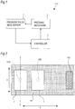
- Fig. 1 is a block diagram showing the configuration of a blood pressure measurement device 100 which is a biological information measurement device for illustrating an embodiment of the invention.
- the blood pressure measurement device 100 is of the wrist wearing type which is used while attached to the wrist.
- the blood pressure measurement device 100 includes: pressure pulse wave sensors 1; a pressing mechanism 2 for pressing the pressure pulse wave sensor 1 against the body surface of the subject; and a controller 3 which controls the pressing mechanism based on a signal output from the pressure pulse wave sensors 1, and which calculates biological information including the blood pressure of the subject, based on the signal.
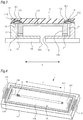
- Fig. 2 is a plan view of a flexible substrate 16 on which the pressure pulse wave sensors 1 shown in Fig. 1 are mounted.
- the flexible substrate 16 is formed into a rectangular shape in which a direction Y perpendicular to a direction X that is one direction coincides with the longitudinal direction.
- Two pressure pulse wave sensors 1 and a connector 16C are mounted on the surface of the substrate.
- the flexible substrate 16 wirings connected respectively to electric terminals of the two pressure pulse wave sensors 1 are disposed in a resin film. The wirings are led to the connector 16C.
- the connector 16C is connected to a connector of a circuit board which is not shown, and on which the controller 3 of Fig. 1 and the like are formed.
- the flexible substrate 16 has through holes 16A, 16B in substantially middles of regions where the two pressure pulse wave sensors 1 are mounted, respectively.
- the through holes 16A, 16B will be described later.
- Fig. 3 is a sectional schematic view taken along line A-A shown in Fig. 2 .
- Fig. 4 is a perspective view showing the configuration of main portions as seeing the pressure pulse wave sensor 1 from the side which is to be in contact with the skin. In Fig. 4 , illustration of partial components is omitted. In Fig. 3 , the components other than the flexible substrate 16 constitute the pressure pulse wave sensor 1.
- the pressure pulse wave sensor 1 includes a sensor chip 10, and a container-like substrate 11 which as a concave portion 11A, and in which the sensor chip 10 is fixed to the bottom surface of the concave portion 11A.
- the sensor chip 10 includes a semiconductor substrate 10A made of a single crystal of silicon, that of a compound semiconductor such as gallium arsenide, or the like.
- the semiconductor substrate 10A is formed into a rectangular shape in which the direction X coincides with the longitudinal direction.
- the substrate 11 is configured by a rigid substrate which is sufficiently higher in rigidity than the semiconductor substrate 10A, such as a ceramic substrate, a glass substrate, or the like.
- the substrate 11 is formed into a rectangular shape in which the direction X coincides with the longitudinal direction.
- a plurality of pressure-sensitive elements S each of which is configured by a bridge having four piezoresistance portions, and which are used for sensing a contact pressure are arranged along the direction X on the surface (the surface on the side which is to be in contact with the skin of a living body) of the semiconductor substrate 10A.
- a pressure-sensitive element row 10D is configured by the plurality of pressure-sensitive elements S which are arranged in the direction X.
- illustration of the pressure-sensitive elements S is omitted.
- a concave portion 10a which is recessed in the direction (hereinafter, referred to as the sensor pressing direction) perpendicular to the pressure-sensitive surface is formed.
- the concave portion 10a causes the semiconductor substrate 10A to have a configuration including a thin portion (diaphragm) in which the thickness in the sensor pressing direction is smaller than that of the other portion. Then, the pressure-sensitive element row 10D is formed in a region of the pressure-sensitive surface which is on the side opposite to the bottom surface of the concave portion 10a.
- a portion which is of the surface opposite to the pressure-sensitive surface of the semiconductor substrate 10A, and which is other than the concave portion 10a is fixed to the bottom surface of the concave portion 11A of the substrate 11 by an adhesive material 12.
- an adhesive material 12 for example, an ultraviolet curable resin is used.
- the semiconductor substrate 10A is fixed to the bottom surface of the concave portion 11A of the rigid substrate 11 so that the concave portion 10a of the semiconductor substrate 10A communicates with the atmosphere only through a through hole 11D which is formed in the bottom surface of the concave portion 11A of the rigid substrate 11.
- One pressure pulse wave sensor 1 of the two pressure pulse wave sensors 1 of the blood pressure measurement device 100 is mounted on the flexible substrate 16 so that the through hole 11D and the through hole 16A overlap with each other in a plan view as seen from the side of the pressure-sensitive surface.
- the other pressure pulse wave sensor 1 of the two pressure pulse wave sensors 1 of the blood pressure measurement device 100 is mounted on the flexible substrate 16 so that the through hole 11D and the through hole 16B overlap with each other in the plan view.
- a space which is in the pressure pulse wave sensor 1, and which is defined by the semiconductor substrate 10A, the adhesive material 12, and the substrate 11 is kept at atmospheric pressure (reference pressure) by the through hole 11D of the substrate 11, and the through hole 16A (or the through hole 16B) of the flexible substrate 16.
- a first terminal portion 10B and second terminal portion 10C which are electrically connected to the pressure-sensitive element row 10D are placed in both end portions of the pressure-sensitive surface of the semiconductor substrate 10A in the direction X.
- Each of the first terminal portion 10B and the second terminal portion 10C is configured by a plurality of electrode pads which are arranged in a direction Y that is perpendicular to the direction X.
- the pressure-sensitive surface of the semiconductor substrate 10A, and the surface of the substrate 11 in which the concave portion 11A is formed are at the same height with respect to the bottom surface of the concave portion 11A of the substrate 11 in the direction perpendicular to the pressure-sensitive surface.
- the pressure-sensitive surface of the semiconductor substrate 10A, and the surface of the substrate 11 in which the concave portion 11A is formed may not be at the strictly same height, and may have a tolerance.
- a third terminal portion 11B for being electrically connected to the first terminal portion 10B, and a fourth terminal portion 11C for being electrically connected to the second terminal portion 10C are disposed on the surface of the substrate 11 in which the concave portion 11A is formed.
- the third terminal portion 11B, the first terminal portion 10B, the second terminal portion 10C, and the fourth terminal portion 11C are arranged in this order along the direction X.
- Each of the third terminal portion 11B and the fourth terminal portion 11C is configured by a plurality of electrode pads which are arranged in the direction Y that is perpendicular to the direction X.
- Each of the terminals of the third terminal portion 11B corresponds to one of the terminals of the first terminal portion 10B.
- Each of the terminals of the fourth terminal portion 11C corresponds to one of the terminals of the second terminal portion 10C.
- the terminals of the first terminal portion 10B are electrically connected to those of the third terminal portion 11B corresponding thereto by wires W1 which are the first electroconductive members.
- the terminals of the second terminal portion 10C are electrically connected to those of the fourth terminal portion 11C corresponding thereto by wires W2 which are the second electroconductive members.
- connection terminals which are connected to the terminals of the third terminal portion 11B, and connection terminals which are connected to the terminals of the fourth terminal portion 11C are exposedly disposed on the surface on the side of the flexible substrate 16. These connection terminals are connected to wiring terminals of the flexible substrate 16.
- the peripheries of the wires W1 and the wires W2 are separately covered and protected by protective members 13.
- a resin such as an epoxy or silicone resin is used as the protective members 13.
- As the resin material for protecting the wires a resin which is largely changed in volume depending on environmental conditions such as the temperature and the humidity is often used.
- the gap between side surface of the concave portion 11A of the substrate 11, and the semiconductor substrate 10A and the adhesive material 12 is filled with a material 14 which is less changed in volume than the protective members 13 depending on the temperature and the humidity.
- a material 14 for example, a resin such as a silicone resin is used.
- the pressure-sensitive surface of the semiconductor substrate 10A, the protective member 13 for the wires W1, and the protective member 13 for the wires W2 are covered by a surface coating layer 15 for protecting the surface of the pressure pulse wave sensor 1.
- the surface coating layer 15 is configured by, for example, a silicone resin.
- the thus configured pressure pulse wave sensor 1 is used while the pressure-sensitive surface of the semiconductor substrate 10A on which the pressure-sensitive element row 10D is formed is pressed through the surface coating layer 15 against the body surface of a living body in a state where the pressure-sensitive element row 10D is located directly above an artery, and the direction X intersects (preferably, is perpendicular to) the traveling direction of the artery. From each of the pressure-sensitive elements S, therefore, an electric signal corresponding to distortion applied to the thin portion of the semiconductor substrate 10A, i.e., a signal indicating the pressure variation acting on the pressure-sensitive element S is output.
- the controller 3 determines the optimum pressure-sensitive element and the optimum pressing force based on the signals output from the pressure pulse wave sensor 1, while adjusting the state of the pressurization which is applied on the body surface through the pressure pulse wave sensor 1 by the pressing mechanism 2. Thereafter, the controller measures the pressure pulse wave based on the signal which is output from the optimum pressure-sensitive element at the optimum pressing force, and calculates biological information such as the blood pressure value and the pulse rate based on the pressure pulse wave.
- the height of the pressure-sensitive surface on which the first terminal portion 10B and the second terminal portion 10C are formed, and that of the surface of the substrate 11 on which the third terminal portion 11B and the fourth terminal portion 11C are formed are substantially equal to each other.
- the wires W1 and the wires W2 can be shortened in length. As a result, the amount of the material of the protective members 13 for covering the wires W1, W2 can be reduced.
- the pressure pulse wave sensor 1 As described above, a material which is largely changed in volume depending on changes of the temperature and the humidity is often used in the protective members 13. According to the pressure pulse wave sensor 1, the amount of the material can be reduced, and, even when a volume change occurs in the protective members 13 depending on the environmental conditions, therefore, the influence of a stress due to the volume change on the sensor chip 10 can be made small. Consequently, the accuracy of detecting a pressure pulse wave can be prevented from being lowered due to a change of the use environment.
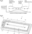
- the pressure pulse wave sensor 1 has the configuration where the protective members 13 are disposed in the both end sides in the direction X of the pressure-sensitive element row 10D. Therefore, the detection sensitivities of the pressure-sensitive elements S of the pressure-sensitive element row 10D are varied as shown in Fig. 5 by the influence of a stress of the protective members 13.
- Fig. 5 shows ideal sensitivity characteristics in which the detection sensitivities of the pressure-sensitive elements S are constant, sensitivity characteristics of the pressure-sensitive element row 10D in the case where a compression stress is generated by the protective members 13, and those of the pressure-sensitive element row 10D in the case where a tensile stress is generated by the protective members 13.
- the sensor chip disclosed in Patent Literature 2 has the configuration where the wiring protective member is disposed on the both sides of each of the pressure-sensitive elements of the pressure-sensitive element row.
- the pressure-sensitive elements are affected in an approximately same manner by a stress produced by deformation of the wiring protective member. Even when the volume of the wiring protective member is largely changed, therefore, the detection sensitivity dispersion in the pressure-sensitive element row can be set within an allowable range.
- the pressure pulse wave sensor 1 has the configuration where the protective members 13 are disposed on the both sides in the direction X of the pressure-sensitive element row 10D. As shown in Fig. 5 , therefore, the manner in which a stress is applied to the respective pressure-sensitive elements is largely varied depending on the position. Consequently, the configuration of the embodiment in which the volume change in the protective members 13 can be remarkably reduced is very effective.
- the wires and the protective members do not exist in portions where the sensor may possibly overlap with an artery, and the portions are flat. Therefore, a pressure pulse wave is easily transmitted to the pressure-sensitive element row 10D, and the accuracy of detecting a pressure pulse wave can be improved.
- the gaps between the end surfaces in the direction X of the sensor chip 10 and the substrate 11 are filled with the material 14 which is less changed in volume than the protective members 13 depending on the temperature and the humidity.
- an influence of a stress which is caused by distortion of the substrate 11, and which acts on the sensor chip 10 can be weakened by the material 14.
- the material of the protective members 13 does not flow in the gaps when the protective members 13 are formed. As compared with a configuration where the material 14 is not used, therefore, the use amount of the material of the protective members 13 can be reduced, and the accuracy of detecting a pressure pulse wave can be prevented from being lowered.
- the sensor chip 10 In the case of a configuration where the material 14 is not used, the sensor chip 10 must be fixed to the substrate 11 in order to minimize the gaps between the sensor chip 10 and the substrate 11. Therefore, the accuracy of fixation of the sensor chip 10 to the substrate 11, and the dimension accuracies of the sensor chip 10 and the substrate 11 are required to be high, and the production cost of a pressure pulse wave sensor is increased.
- the fixation accuracy and the dimension accuracies may not be so high, and therefore the production cost can be prevented from being increased.
- the height of the pressure-sensitive surface on which the first terminal portion 10B and the second terminal portion 10C are formed may be larger than that of the surface of the substrate 11 on which the third terminal portion 11B and the fourth terminal portion 11C are formed.
- the height of the pressure-sensitive surface on which the first terminal portion 10B and the second terminal portion 10C are formed may be smaller than that of the surface of the substrate 11 on which the third terminal portion 11B and the fourth terminal portion 11C are formed.
- the distance between the surface of the sensor chip 10 and the substrate surface is about 400 ⁇ m.
- the pressure pulse wave sensor 1 when, with respect to the bottom surface of the concave portion 11A, the difference between the height of the pressure-sensitive surface on which the first terminal portion 10B and the second terminal portion 10C are formed, and that of the surface of the substrate 11 on which the third terminal portion 11B and the fourth terminal portion 11C are formed is sufficiently smaller than 400 ⁇ m (preferably, zero), the volume of the protective members 13 can be reduced, and an influence of a stress which acts on the accuracy of detecting a pressure pulse wave can be weakened.
- the pressure pulse wave sensor 1 has a configuration where, in both end portions in the direction X of the pressure-sensitive surface of the semiconductor substrate 10A, chip-side terminal portions configured by the first terminal portion 10B and the second terminal portion 10C are disposed, and substrate-side terminal portions configured by the third terminal portion 11B and fourth terminal portion 11C which correspond respectively to the first terminal portion 10B and the second terminal portion 10C are disposed.
- a configuration where a chip-side terminal portion 10E configured by terminals which are electrically connected to the pressure-sensitive elements S is disposed in only one of both end portions in the direction X of the pressure-sensitive surface of the semiconductor substrate 10A may be employed.
- a substrate-side terminal portion 11E configured by terminals for being electrically connected to terminals of the chip-side terminal portion 10E may be formed on the surface which is on the side opposite in the direction X to the pressure-sensitive element row 10D while setting the chip-side terminal portion 10E as a boundary, and in which the concave portion 11A of the substrate 11 is formed.
- the configuration where, as shown in Fig. 4 , the chip-side terminal portions configured by the first terminal portion 10B and the second terminal portion 10C are disposed in the both end portions of the pressure-sensitive surface of the semiconductor substrate 10A in the direction X, the width in the direction Y of the sensor chip 10 is not required to be made so large. Therefore, the configuration is advantageous to miniaturize the pressure pulse wave sensor 1.
- the blood pressure measurement device of the wrist wearing type which detects the pressure pulse wave of the radial artery in the wrist has been described.
- a measurement device which is to be applied to the carotid artery or the dorsalis pedis artery may be possible.
- the pressure-sensitive elements S which detect a contact pressure are not limited to elements in which a bridge circuit and a diaphragm are employed, and may use elements having another well-known configuration.
- the blood pressure measurement device 100 includes the two pressure pulse wave sensors 1. When at least one pressure pulse wave sensor 1 is provided, the pressure pulse wave can be detected, and biological information can be measured.
- the substrate 11 may have a structure in which, among the side walls of the concave portion 11A, the side walls at the both ends in the direction Y are removed away. Namely, the substrate 11 may have a substantially U-like shape.
- the concave portion 11A has a rectangular parallelepiped shape, and the substrate 11 is formed into a container-like shape, there is no fear that the material 14 leaks to the outside in a step of filling the gaps between the substrate 11 and the sensor chip 10 with the material 14. Therefore, the pressure pulse wave sensor 1 can be easily produced.
- the means for connecting the terminals of the first terminal portion 10B with those of the third terminal portion 11B which corresponds to it is not limited to wires, and may be electro conductive members such as electroconductive paste.
- the means for connecting the terminals of the second terminal portion 10C with those of the fourth terminal portion 11C which corresponds to it is not limited to wires, and may be electroconductive members such as electroconductive paste. Even in a case where the connections are performed by using any kind of electroconductive members, the protective members 13 for protecting the wirings formed by the electroconductive members are necessary, and therefore the invention is effective.
- the pressure pulse wave sensor 1 may have a configuration where only the gaps between the end surfaces of the sensor chip 10 in the direction X and the substrate 11 are filled with the material 14. When the gaps are filled with the material 14, in the formation of the protective members 13, it is possible to attain an effect that the volume increase of the protective members 13 due to the flowing of the protective members 13 in the gaps can be prevented from occurring.
- the disclosed pressure pulse wave sensor includes: a sensor chip which includes: a pressure-sensitive element row configured by a plurality of pressure-sensitive elements that are arranged in one direction; and a chip-side terminal portion that is placed in an end portion in the one direction of a pressure-sensitive surface on which the pressure-sensitive element row is formed, and that is electrically connected to the pressure-sensitive element row, the sensor chip to be used while the pressure-sensitive surface is pressed against a body surface of a living body in a state where the one direction intersects a traveling direction of an artery of the living body; and a substrate which includes a concave portion, the sensor chip fixed to a bottom surface of the concave portion, a substrate-side terminal portion for being electrically connected to the chip-side terminal portion is disposed on a surface of the substrate in which the concave portion is formed, and the pressure pulse wave sensor further includes: an electroconductive member which connects the chip-side terminal portion and the substrate-side terminal portion to each other; and a protective member which covers the electroconductive member.
- the chip-side terminal portion is configured by a first terminal portion and second terminal portion which are placed in both end portions in the one direction of a pressure-sensitive surface, respectively
- the substrate-side terminal portion is configured by a third terminal portion for being electrically connected to the first terminal portion, and a fourth terminal portion for being electrically connected to the second terminal portion, in a plan view as seen in a direction perpendicular to the pressure-sensitive surface, the third terminal portion, the first terminal portion, the second terminal portion, and the fourth terminal portion are arranged in this order along the one direction
- the electroconductive member is configured by a first electroconductive member which connects the first terminal portion and the third terminal portion to each other, and a second electroconductive member which connects the second terminal portion and the fourth terminal portion to each other
- the protective member covers the first electroconductive member and the second electroconductive member in a separate manner.
- a height of the pressure-sensitive surface on which the chip-side terminal portion is formed, and a height of the surface of the substrate on which the substrate-side terminal portion is formed are equal to each other.
- a gap between an end surface in the one direction of the sensor chip and the substrate is filled with a material which is less changed in volume than the protective member depending on a temperature and a humidity.
- the disclosed biological information measurement device includes: the pressure pulse wave sensor; and a biological information calculating section which is configured to calculate biological information based on a pressure pulse wave detected by the pressure pulse wave sensor.
- a pressure pulse wave sensor in which the accuracy of detecting a pressure pulse wave can be prevented from being lowered due to a change of the use environment, and a biological information measurement device which includes the sensor.
Landscapes
- Health & Medical Sciences (AREA)
- Life Sciences & Earth Sciences (AREA)
- Cardiology (AREA)
- Physics & Mathematics (AREA)
- Biomedical Technology (AREA)
- Heart & Thoracic Surgery (AREA)
- Vascular Medicine (AREA)
- Veterinary Medicine (AREA)
- Public Health (AREA)
- Biophysics (AREA)
- Pathology (AREA)
- Engineering & Computer Science (AREA)
- General Health & Medical Sciences (AREA)
- Animal Behavior & Ethology (AREA)
- Medical Informatics (AREA)
- Molecular Biology (AREA)
- Surgery (AREA)
- Physiology (AREA)
- Ophthalmology & Optometry (AREA)
- General Physics & Mathematics (AREA)
- Dentistry (AREA)
- Analytical Chemistry (AREA)
- Chemical & Material Sciences (AREA)
- Measuring Pulse, Heart Rate, Blood Pressure Or Blood Flow (AREA)
Claims (4)
- Druckimpulswellensensor (1), umfassend:einen Sensorchip (10), der ein Halbleitersubstrat (10A) aufweist, das Folgendes aufweist: eine Reihe (10D) aus druckempfindlichen Elementen, die mit einer Vielzahl druckempfindlicher Elemente (S) ausgelegt ist, die in einer Richtung (X) angeordnet sind; und einen chipseitigen Anschlussabschnitt (10B, 10C, 10E), der in der einen Richtung (X) einer druckempfindlichen Fläche, auf der die Reihe (10D) aus druckempfindlichen Elementen ausgebildet ist, in einem Endabschnitt platziert ist und der mit der Reihe (10D) aus druckempfindlichen Elementen elektrisch verbunden ist, wobei das Halbleitersubstrat (10A) ferner einen konkaven Abschnitt (10a) aufweist, der einen dünnen Abschnitt aufweist, in dem eine Dicke in einer Richtung senkrecht zu der druckempfindlichen Fläche geringer ist als eine Dicke eines weiteren Abschnitts, wobei der Sensorchip (10) zu verwenden ist, während die druckempfindliche Fläche in einem Zustand gegen die Oberfläche eines Körpers einer lebenden Person gedrückt wird, in dem die eine Richtung (X) eine Verlaufsrichtung einer Arterie des Körpers der lebenden Person schneidet; undein Substrat (11), das einen konkaven Abschnitt (11A) aufweist, wobei das Halbleitersubstrat (10A) des Sensorchips (10) an einer Bodenfläche des konkaven Abschnitts (11A) befestigt ist,wobeiein substratseitiger Anschlussabschnitt (11B, 11C, 11E) zum elektrischen Anschließen an den chipseitigen Anschlussabschnitt (10B, 10C, 10E) an einer Fläche einer Seitenwand des konkaven Abschnitts (11A) des Substrats (11) angeordnet ist, wobei sich die Fläche in einer vorgegebenen Höhe bezogen auf die Bodenfläche des konkaven Abschnitts (11A) befindet, undder Druckimpulswellensensor (1) ferner umfasst:ein elektrisch leitendes Glied (W1, W2), das den chipseitigen Anschlussabschnitt (10B, 10C, 10E) und den substratseitigen Anschlussabschnitt (11B, 11C, 11E) miteinander verbindet; undein Schutzglied (13), welches das elektrisch leitende Glied (W1, W2) abdeckt,dadurch gekennzeichnet, dassein Zwischenraum zwischen einer Endfläche in der einen Richtung (X) des Sensorchips (10) und dem Substrat (11) mit einem Material (14) gefüllt ist, dessen Volumen sich je nach Temperatur und Feuchtigkeit weniger stark verändert als das des Schutzglieds (13).
- Druckimpulswellensensor (1) nach Anspruch 1, wobei
der chipseitige Anschlussabschnitt (10B, 10C, 10E) mit einem ersten Anschlussabschnitt (10B) und einem zweiten Anschlussabschnitt (10C) ausgelegt ist, die jeweils in einem Endabschnitt in der einen Richtung (X) der druckempfindlichen Fläche platziert sind,
der substratseitige Anschlussabschnitt (11B, 11C, 11E) mit einem dritten Anschlussabschnitt (11B) für den elektrischen Anschluss an den ersten Anschlussabschnitt (10B) und einem vierten Anschlussabschnitt (11C) für den elektrischen Anschluss an den zweiten Anschlussabschnitt (10C) ausgelegt ist,
in einer Draufsicht in einer Richtung senkrecht zur druckempfindlichen Fläche betrachtet der dritte Anschussabschnitt (11B), der erste Anschlussabschnitt (10B), der zweite Anschlussabschnitt (10C) und der vierte Anschlussabschnitt (11C) in dieser Reihenfolge die eine Richtung (X) entlang angeordnet sind,
das elektrisch leitende Glied (W1, W2) mit einem ersten elektrisch leitenden Glied (W1), das den ersten Anschlussabschnitt (10B) und den dritten Anschlussabschnitt (11B) miteinander verbindet, und einem zweiten elektrisch leitenden Glied (W2) ausgelegt ist, das den zweiten Anschlussabschnitt (10C) und den vierten Anschlussabschnitt (11C) miteinander verbindet, und
das Schutzglied (13) das erste elektrisch leitende Glied (W1) und das zweite elektrisch leitende Glied (W2) separat abdeckt. - Druckimpulswellensensor (1) nach Anspruch 1 oder 2, wobei bezogen auf die Bodenfläche des konkaven Abschnitts (11A) eine Höhe der druckempfindlichen Fläche, auf der der chipseitige Anschlussabschnitt (10B, 10C, 10E) ausgebildet ist, und eine Höhe der Fläche des Substrats (11), auf der der substratseitige Anschlussabschnitt (11B, 11C, 11E) angeordnet ist, einander entsprechen.
- Vorrichtung zur Messung biologischer Informationen (100), umfassend:den Druckimpulswellensensor (1) nach einem der Ansprüche 1 bis 3 undeinen Abschnitt zur Berechnung biologischer Informationen (3), der so eingerichtet ist, dass er biologische Informationen auf Grundlage einer Druckimpulswelle berechnet, die der Druckimpulswellensensor (1) erfasst.
Applications Claiming Priority (2)
| Application Number | Priority Date | Filing Date | Title |
|---|---|---|---|
| JP2015164697A JP6528602B2 (ja) | 2015-08-24 | 2015-08-24 | 圧脈波センサ及び生体情報測定装置 |
| PCT/JP2016/073325 WO2017033730A1 (ja) | 2015-08-24 | 2016-08-08 | 圧脈波センサ及び生体情報測定装置 |
Publications (3)
| Publication Number | Publication Date |
|---|---|
| EP3320835A1 EP3320835A1 (de) | 2018-05-16 |
| EP3320835A4 EP3320835A4 (de) | 2019-02-27 |
| EP3320835B1 true EP3320835B1 (de) | 2020-06-24 |
Family
ID=58100118
Family Applications (1)
| Application Number | Title | Priority Date | Filing Date |
|---|---|---|---|
| EP16839077.1A Active EP3320835B1 (de) | 2015-08-24 | 2016-08-08 | Druckimpulswellensensor und vorrichtung zur messung biologischer informationen |
Country Status (5)
| Country | Link |
|---|---|
| US (1) | US11344207B2 (de) |
| EP (1) | EP3320835B1 (de) |
| JP (1) | JP6528602B2 (de) |
| CN (1) | CN108024731B (de) |
| WO (1) | WO2017033730A1 (de) |
Families Citing this family (1)
| Publication number | Priority date | Publication date | Assignee | Title |
|---|---|---|---|---|
| WO2021106227A1 (ja) * | 2019-11-29 | 2021-06-03 | 村田機械株式会社 | 接圧センサ、それを備えたニット製品、および接圧センサの製造方法 |
Family Cites Families (14)
| Publication number | Priority date | Publication date | Assignee | Title |
|---|---|---|---|---|
| JP3039934B2 (ja) * | 1989-06-13 | 2000-05-08 | コーリン電子株式会社 | 圧脈波検出装置 |
| JPH03186247A (ja) * | 1989-12-16 | 1991-08-14 | Koorin Denshi Kk | 脈波検出装置 |
| JP2798764B2 (ja) * | 1990-01-09 | 1998-09-17 | コーリン電子株式会社 | 半導体圧脈波センサ |
| US5179956A (en) * | 1990-07-06 | 1993-01-19 | Colin Electronics Co., Ltd. | Contact pressure sensor |
| JP3115430B2 (ja) * | 1992-09-11 | 2000-12-04 | 日本コーリン株式会社 | 脈波検出装置 |
| US5797850A (en) * | 1993-11-09 | 1998-08-25 | Medwave, Inc. | Method and apparatus for calculating blood pressure of an artery |
| DE69832782T2 (de) * | 1997-11-20 | 2006-09-21 | Seiko Epson Corp. | Vorrichtung zur pulswellenuntersuchung |
| JP2000287944A (ja) | 1999-04-06 | 2000-10-17 | Tokai Rika Co Ltd | カテーテル用圧力センサブロック |
| JP4363157B2 (ja) | 2002-11-29 | 2009-11-11 | オムロンヘルスケア株式会社 | 脈波測定装置 |
| JP2004361308A (ja) | 2003-06-06 | 2004-12-24 | Fuji Electric Device Technology Co Ltd | 物理量検出装置および物理量検出手段格納ケース |
| JP2007301232A (ja) | 2006-05-12 | 2007-11-22 | Omron Healthcare Co Ltd | 圧脈波センサおよびこれを備えた脈波測定装置 |
| JP2008136655A (ja) * | 2006-12-01 | 2008-06-19 | Omron Healthcare Co Ltd | 脈波測定用電極ユニットおよび脈波測定装置 |
| US9642567B2 (en) | 2012-08-09 | 2017-05-09 | Konica Minolta, Inc. | Biological information measurement device and pulse oximeter |
| JP6256058B2 (ja) | 2014-01-31 | 2018-01-10 | オムロンヘルスケア株式会社 | 脈波検出装置 |
-
2015
- 2015-08-24 JP JP2015164697A patent/JP6528602B2/ja active Active
-
2016
- 2016-08-08 WO PCT/JP2016/073325 patent/WO2017033730A1/ja active Application Filing
- 2016-08-08 CN CN201680047186.3A patent/CN108024731B/zh active Active
- 2016-08-08 EP EP16839077.1A patent/EP3320835B1/de active Active
-
2018
- 2018-02-09 US US15/893,469 patent/US11344207B2/en active Active
Non-Patent Citations (1)
| Title |
|---|
| None * |
Also Published As
| Publication number | Publication date |
|---|---|
| US20180160919A1 (en) | 2018-06-14 |
| JP2017042207A (ja) | 2017-03-02 |
| WO2017033730A1 (ja) | 2017-03-02 |
| CN108024731A (zh) | 2018-05-11 |
| CN108024731B (zh) | 2020-12-15 |
| EP3320835A1 (de) | 2018-05-16 |
| EP3320835A4 (de) | 2019-02-27 |
| JP6528602B2 (ja) | 2019-06-12 |
| US11344207B2 (en) | 2022-05-31 |
Similar Documents
| Publication | Publication Date | Title |
|---|---|---|
| US8316725B2 (en) | Force sensor | |
| US6255728B1 (en) | Rigid encapsulation package for semiconductor devices | |
| EP2189773B1 (de) | Design eines Nass/Nass-Differenzdrucksensors auf Grundlage eines Mikroelektronik-Verpackungsverfahrens | |
| US10136858B2 (en) | Method for inspecting pressure pulse wave sensor and method for manufacturing pressure pulse wave sensor | |
| US10144636B2 (en) | Method of manufacturing a sensor | |
| EP3320835B1 (de) | Druckimpulswellensensor und vorrichtung zur messung biologischer informationen | |
| EP3660476B1 (de) | Kostengünstiger umgossener leiterrahmen-kraftsensor mit mehreren montagepositionen | |
| US20120206888A1 (en) | Sensor arrangement and chip comprising additional fixing pins | |
| US20180160918A1 (en) | Pulse wave measurement device | |
| CN107250751B (zh) | 液压传感器、液压控制单元和组件以及车辆制动系统 | |
| KR20110059028A (ko) | 반도체 스트레인게이지형 압력센서모듈과 그 제조방법 | |
| JP2003262560A (ja) | 圧力センサ |
Legal Events
| Date | Code | Title | Description |
|---|---|---|---|
| STAA | Information on the status of an ep patent application or granted ep patent |
Free format text: STATUS: THE INTERNATIONAL PUBLICATION HAS BEEN MADE |
|
| PUAI | Public reference made under article 153(3) epc to a published international application that has entered the european phase |
Free format text: ORIGINAL CODE: 0009012 |
|
| STAA | Information on the status of an ep patent application or granted ep patent |
Free format text: STATUS: REQUEST FOR EXAMINATION WAS MADE |
|
| 17P | Request for examination filed |
Effective date: 20180209 |
|
| AK | Designated contracting states |
Kind code of ref document: A1 Designated state(s): AL AT BE BG CH CY CZ DE DK EE ES FI FR GB GR HR HU IE IS IT LI LT LU LV MC MK MT NL NO PL PT RO RS SE SI SK SM TR |
|
| AX | Request for extension of the european patent |
Extension state: BA ME |
|
| DAV | Request for validation of the european patent (deleted) | ||
| DAX | Request for extension of the european patent (deleted) | ||
| A4 | Supplementary search report drawn up and despatched |
Effective date: 20190128 |
|
| RIC1 | Information provided on ipc code assigned before grant |
Ipc: A61B 5/022 20060101ALI20190122BHEP Ipc: A61B 5/021 20060101ALI20190122BHEP Ipc: A61B 5/02 20060101AFI20190122BHEP Ipc: A61B 5/00 20060101ALI20190122BHEP |
|
| GRAP | Despatch of communication of intention to grant a patent |
Free format text: ORIGINAL CODE: EPIDOSNIGR1 |
|
| STAA | Information on the status of an ep patent application or granted ep patent |
Free format text: STATUS: GRANT OF PATENT IS INTENDED |
|
| INTG | Intention to grant announced |
Effective date: 20200108 |
|
| GRAS | Grant fee paid |
Free format text: ORIGINAL CODE: EPIDOSNIGR3 |
|
| GRAA | (expected) grant |
Free format text: ORIGINAL CODE: 0009210 |
|
| STAA | Information on the status of an ep patent application or granted ep patent |
Free format text: STATUS: THE PATENT HAS BEEN GRANTED |
|
| AK | Designated contracting states |
Kind code of ref document: B1 Designated state(s): AL AT BE BG CH CY CZ DE DK EE ES FI FR GB GR HR HU IE IS IT LI LT LU LV MC MK MT NL NO PL PT RO RS SE SI SK SM TR |
|
| REG | Reference to a national code |
Ref country code: GB Ref legal event code: FG4D |
|
| REG | Reference to a national code |
Ref country code: CH Ref legal event code: EP |
|
| REG | Reference to a national code |
Ref country code: AT Ref legal event code: REF Ref document number: 1283069 Country of ref document: AT Kind code of ref document: T Effective date: 20200715 |
|
| REG | Reference to a national code |
Ref country code: DE Ref legal event code: R096 Ref document number: 602016038879 Country of ref document: DE |
|
| REG | Reference to a national code |
Ref country code: IE Ref legal event code: FG4D |
|
| PG25 | Lapsed in a contracting state [announced via postgrant information from national office to epo] |
Ref country code: LT Free format text: LAPSE BECAUSE OF FAILURE TO SUBMIT A TRANSLATION OF THE DESCRIPTION OR TO PAY THE FEE WITHIN THE PRESCRIBED TIME-LIMIT Effective date: 20200624 Ref country code: FI Free format text: LAPSE BECAUSE OF FAILURE TO SUBMIT A TRANSLATION OF THE DESCRIPTION OR TO PAY THE FEE WITHIN THE PRESCRIBED TIME-LIMIT Effective date: 20200624 Ref country code: GR Free format text: LAPSE BECAUSE OF FAILURE TO SUBMIT A TRANSLATION OF THE DESCRIPTION OR TO PAY THE FEE WITHIN THE PRESCRIBED TIME-LIMIT Effective date: 20200925 Ref country code: NO Free format text: LAPSE BECAUSE OF FAILURE TO SUBMIT A TRANSLATION OF THE DESCRIPTION OR TO PAY THE FEE WITHIN THE PRESCRIBED TIME-LIMIT Effective date: 20200924 Ref country code: SE Free format text: LAPSE BECAUSE OF FAILURE TO SUBMIT A TRANSLATION OF THE DESCRIPTION OR TO PAY THE FEE WITHIN THE PRESCRIBED TIME-LIMIT Effective date: 20200624 |
|
| REG | Reference to a national code |
Ref country code: LT Ref legal event code: MG4D |
|
| PG25 | Lapsed in a contracting state [announced via postgrant information from national office to epo] |
Ref country code: LV Free format text: LAPSE BECAUSE OF FAILURE TO SUBMIT A TRANSLATION OF THE DESCRIPTION OR TO PAY THE FEE WITHIN THE PRESCRIBED TIME-LIMIT Effective date: 20200624 Ref country code: RS Free format text: LAPSE BECAUSE OF FAILURE TO SUBMIT A TRANSLATION OF THE DESCRIPTION OR TO PAY THE FEE WITHIN THE PRESCRIBED TIME-LIMIT Effective date: 20200624 Ref country code: HR Free format text: LAPSE BECAUSE OF FAILURE TO SUBMIT A TRANSLATION OF THE DESCRIPTION OR TO PAY THE FEE WITHIN THE PRESCRIBED TIME-LIMIT Effective date: 20200624 Ref country code: BG Free format text: LAPSE BECAUSE OF FAILURE TO SUBMIT A TRANSLATION OF THE DESCRIPTION OR TO PAY THE FEE WITHIN THE PRESCRIBED TIME-LIMIT Effective date: 20200924 |
|
| REG | Reference to a national code |
Ref country code: NL Ref legal event code: MP Effective date: 20200624 |
|
| REG | Reference to a national code |
Ref country code: AT Ref legal event code: MK05 Ref document number: 1283069 Country of ref document: AT Kind code of ref document: T Effective date: 20200624 |
|
| PG25 | Lapsed in a contracting state [announced via postgrant information from national office to epo] |
Ref country code: NL Free format text: LAPSE BECAUSE OF FAILURE TO SUBMIT A TRANSLATION OF THE DESCRIPTION OR TO PAY THE FEE WITHIN THE PRESCRIBED TIME-LIMIT Effective date: 20200624 Ref country code: AL Free format text: LAPSE BECAUSE OF FAILURE TO SUBMIT A TRANSLATION OF THE DESCRIPTION OR TO PAY THE FEE WITHIN THE PRESCRIBED TIME-LIMIT Effective date: 20200624 |
|
| PG25 | Lapsed in a contracting state [announced via postgrant information from national office to epo] |
Ref country code: IT Free format text: LAPSE BECAUSE OF FAILURE TO SUBMIT A TRANSLATION OF THE DESCRIPTION OR TO PAY THE FEE WITHIN THE PRESCRIBED TIME-LIMIT Effective date: 20200624 Ref country code: PT Free format text: LAPSE BECAUSE OF FAILURE TO SUBMIT A TRANSLATION OF THE DESCRIPTION OR TO PAY THE FEE WITHIN THE PRESCRIBED TIME-LIMIT Effective date: 20201026 Ref country code: EE Free format text: LAPSE BECAUSE OF FAILURE TO SUBMIT A TRANSLATION OF THE DESCRIPTION OR TO PAY THE FEE WITHIN THE PRESCRIBED TIME-LIMIT Effective date: 20200624 Ref country code: AT Free format text: LAPSE BECAUSE OF FAILURE TO SUBMIT A TRANSLATION OF THE DESCRIPTION OR TO PAY THE FEE WITHIN THE PRESCRIBED TIME-LIMIT Effective date: 20200624 Ref country code: SM Free format text: LAPSE BECAUSE OF FAILURE TO SUBMIT A TRANSLATION OF THE DESCRIPTION OR TO PAY THE FEE WITHIN THE PRESCRIBED TIME-LIMIT Effective date: 20200624 Ref country code: RO Free format text: LAPSE BECAUSE OF FAILURE TO SUBMIT A TRANSLATION OF THE DESCRIPTION OR TO PAY THE FEE WITHIN THE PRESCRIBED TIME-LIMIT Effective date: 20200624 Ref country code: CZ Free format text: LAPSE BECAUSE OF FAILURE TO SUBMIT A TRANSLATION OF THE DESCRIPTION OR TO PAY THE FEE WITHIN THE PRESCRIBED TIME-LIMIT Effective date: 20200624 Ref country code: ES Free format text: LAPSE BECAUSE OF FAILURE TO SUBMIT A TRANSLATION OF THE DESCRIPTION OR TO PAY THE FEE WITHIN THE PRESCRIBED TIME-LIMIT Effective date: 20200624 |
|
| PG25 | Lapsed in a contracting state [announced via postgrant information from national office to epo] |
Ref country code: SK Free format text: LAPSE BECAUSE OF FAILURE TO SUBMIT A TRANSLATION OF THE DESCRIPTION OR TO PAY THE FEE WITHIN THE PRESCRIBED TIME-LIMIT Effective date: 20200624 Ref country code: PL Free format text: LAPSE BECAUSE OF FAILURE TO SUBMIT A TRANSLATION OF THE DESCRIPTION OR TO PAY THE FEE WITHIN THE PRESCRIBED TIME-LIMIT Effective date: 20200624 Ref country code: IS Free format text: LAPSE BECAUSE OF FAILURE TO SUBMIT A TRANSLATION OF THE DESCRIPTION OR TO PAY THE FEE WITHIN THE PRESCRIBED TIME-LIMIT Effective date: 20201024 |
|
| REG | Reference to a national code |
Ref country code: DE Ref legal event code: R097 Ref document number: 602016038879 Country of ref document: DE |
|
| PG25 | Lapsed in a contracting state [announced via postgrant information from national office to epo] |
Ref country code: MC Free format text: LAPSE BECAUSE OF FAILURE TO SUBMIT A TRANSLATION OF THE DESCRIPTION OR TO PAY THE FEE WITHIN THE PRESCRIBED TIME-LIMIT Effective date: 20200624 |
|
| REG | Reference to a national code |
Ref country code: CH Ref legal event code: PL |
|
| PG25 | Lapsed in a contracting state [announced via postgrant information from national office to epo] |
Ref country code: DK Free format text: LAPSE BECAUSE OF FAILURE TO SUBMIT A TRANSLATION OF THE DESCRIPTION OR TO PAY THE FEE WITHIN THE PRESCRIBED TIME-LIMIT Effective date: 20200624 Ref country code: CH Free format text: LAPSE BECAUSE OF NON-PAYMENT OF DUE FEES Effective date: 20200831 Ref country code: LI Free format text: LAPSE BECAUSE OF NON-PAYMENT OF DUE FEES Effective date: 20200831 Ref country code: LU Free format text: LAPSE BECAUSE OF NON-PAYMENT OF DUE FEES Effective date: 20200808 |
|
| PLBE | No opposition filed within time limit |
Free format text: ORIGINAL CODE: 0009261 |
|
| STAA | Information on the status of an ep patent application or granted ep patent |
Free format text: STATUS: NO OPPOSITION FILED WITHIN TIME LIMIT |
|
| GBPC | Gb: european patent ceased through non-payment of renewal fee |
Effective date: 20200924 |
|
| REG | Reference to a national code |
Ref country code: BE Ref legal event code: MM Effective date: 20200831 |
|
| 26N | No opposition filed |
Effective date: 20210325 |
|
| PG25 | Lapsed in a contracting state [announced via postgrant information from national office to epo] |
Ref country code: FR Free format text: LAPSE BECAUSE OF NON-PAYMENT OF DUE FEES Effective date: 20200824 |
|
| PG25 | Lapsed in a contracting state [announced via postgrant information from national office to epo] |
Ref country code: SI Free format text: LAPSE BECAUSE OF FAILURE TO SUBMIT A TRANSLATION OF THE DESCRIPTION OR TO PAY THE FEE WITHIN THE PRESCRIBED TIME-LIMIT Effective date: 20200624 Ref country code: IE Free format text: LAPSE BECAUSE OF NON-PAYMENT OF DUE FEES Effective date: 20200808 Ref country code: GB Free format text: LAPSE BECAUSE OF NON-PAYMENT OF DUE FEES Effective date: 20200924 Ref country code: BE Free format text: LAPSE BECAUSE OF NON-PAYMENT OF DUE FEES Effective date: 20200831 |
|
| PG25 | Lapsed in a contracting state [announced via postgrant information from national office to epo] |
Ref country code: TR Free format text: LAPSE BECAUSE OF FAILURE TO SUBMIT A TRANSLATION OF THE DESCRIPTION OR TO PAY THE FEE WITHIN THE PRESCRIBED TIME-LIMIT Effective date: 20200624 Ref country code: MT Free format text: LAPSE BECAUSE OF FAILURE TO SUBMIT A TRANSLATION OF THE DESCRIPTION OR TO PAY THE FEE WITHIN THE PRESCRIBED TIME-LIMIT Effective date: 20200624 Ref country code: CY Free format text: LAPSE BECAUSE OF FAILURE TO SUBMIT A TRANSLATION OF THE DESCRIPTION OR TO PAY THE FEE WITHIN THE PRESCRIBED TIME-LIMIT Effective date: 20200624 |
|
| PG25 | Lapsed in a contracting state [announced via postgrant information from national office to epo] |
Ref country code: MK Free format text: LAPSE BECAUSE OF FAILURE TO SUBMIT A TRANSLATION OF THE DESCRIPTION OR TO PAY THE FEE WITHIN THE PRESCRIBED TIME-LIMIT Effective date: 20200624 |
|
| P01 | Opt-out of the competence of the unified patent court (upc) registered |
Effective date: 20230512 |
|
| PGFP | Annual fee paid to national office [announced via postgrant information from national office to epo] |
Ref country code: DE Payment date: 20230627 Year of fee payment: 8 |