EP3317821B1 - Smartcard-rohling mit mindestens einer schnittstelle zur berührungslosen übertragung von informationen - Google Patents
Smartcard-rohling mit mindestens einer schnittstelle zur berührungslosen übertragung von informationen Download PDFInfo
- Publication number
- EP3317821B1 EP3317821B1 EP16757822.8A EP16757822A EP3317821B1 EP 3317821 B1 EP3317821 B1 EP 3317821B1 EP 16757822 A EP16757822 A EP 16757822A EP 3317821 B1 EP3317821 B1 EP 3317821B1
- Authority
- EP
- European Patent Office
- Prior art keywords
- smart card
- electronic component
- antenna
- card blank
- blank
- Prior art date
- Legal status (The legal status is an assumption and is not a legal conclusion. Google has not performed a legal analysis and makes no representation as to the accuracy of the status listed.)
- Active
Links
Images





Classifications
-
- G—PHYSICS
- G06—COMPUTING OR CALCULATING; COUNTING
- G06K—GRAPHICAL DATA READING; PRESENTATION OF DATA; RECORD CARRIERS; HANDLING RECORD CARRIERS
- G06K19/00—Record carriers for use with machines and with at least a part designed to carry digital markings
- G06K19/06—Record carriers for use with machines and with at least a part designed to carry digital markings characterised by the kind of the digital marking, e.g. shape, nature, code
- G06K19/067—Record carriers with conductive marks, printed circuits or semiconductor circuit elements, e.g. credit or identity cards also with resonating or responding marks without active components
- G06K19/07—Record carriers with conductive marks, printed circuits or semiconductor circuit elements, e.g. credit or identity cards also with resonating or responding marks without active components with integrated circuit chips
- G06K19/077—Constructional details, e.g. mounting of circuits in the carrier
- G06K19/07749—Constructional details, e.g. mounting of circuits in the carrier the record carrier being capable of non-contact communication, e.g. constructional details of the antenna of a non-contact smart card
- G06K19/0775—Constructional details, e.g. mounting of circuits in the carrier the record carrier being capable of non-contact communication, e.g. constructional details of the antenna of a non-contact smart card arrangements for connecting the integrated circuit to the antenna
Definitions
- the invention relates to a smartcard blank having at least one interface for non-contact transmission of information, which has a carrier body with a recess into which an electronic component such as a microchip can be inserted, wherein an antenna is provided in the carrier body, which with the in the recess used electronic component is electrically connected, wherein the antenna has at least one connecting element for producing an electrically conductive connection with the electronic component, which is arranged in a first plane in the carrier body of the smartcard blank, of a defined by the electronic component second level is spaced, so that there is a height difference between the electronic component and the connecting element, as well as this smartcard blank referring smart card and a method for its preparation.
- Such a smart card is widely used. It has an often credit-card-sized carrier body, which is provided with a recess into which a microchip is inserted.
- This microchip has a contact-based contact element for forming a first interface or is electrically conductively connected to such a contact element of the smartcard so that an electrically conductive contact between the microchip is achieved by mechanical contact between this contact element and a corresponding contact element of a peripheral device interacting with the smartcard the smartcard and z.
- peripheral device eg. As a terminal, a goods or cash dispenser or the like is produced and this peripheral device can access the data stored on the microchip data, information and / or programs, in particular application programs.
- modern smartcards have, as a second interface, an antenna which is connected in an electrically conductive manner to the microchip and serves to establish a contactless connection between the peripheral device using the smartcard and the microchip, for example by means of an RFID or NFC technology.
- the microchip received in the recess of the card body must be connected to connection elements of the antenna.
- the antenna which surrounds the microchip receiving recess, is arranged in a first plane of the carrier body, which lies under a second plane defined by the microchip. It is therefore given a height difference between the microchip and the connection elements of the antenna, which must be bridged by an electrically conductive connection.
- connection is designed such that an electrically conductive adhesive is used to establish the connection between the microchip and the connection elements of the antenna.
- the manufacturer of the finished smart card thus refers to a smart card blank, in which he then has to use the equipped with the appropriate data and / or programs microchip.
- the chip card has a card body, a cavity machined therefrom, a chip or another module containing electronic components with antenna connection contacts which serve for connection to an antenna or an antenna layer with antenna devices in the card body, the card body having contacts for connecting the chip. It is envisaged that a contact element is provided between the contacts in the card body and the antenna connection contacts, this conductively connecting, which connect the contacts and the antenna connection contacts electrically conductive. It can also be arranged a conductive metallic bolt for this purpose.
- a portable data carrier comprising a data carrier body with an electronic component and an electronic module has. This is at least partially embedded in the data carrier body and electrically connected via a module contact device of the module by means of an elastic, electrically conductive material under pressure to a component contact device of the electronic component of the data carrier.
- the module contact device has a spatially structured design and a spatial structure is embossed into the elastic, electrically conductive material by the spatially structured module contact device.
- the smart card blank at least one connecting element for producing an electrically conductive connection is provided with the lead frame, which extends between the aforementioned first level and the aforementioned second level, and wherein this at least one connecting element has a height which is substantially equal to the height difference between the two aforementioned planes, and that the at least one connection element is part of the antenna connection frame.
- the inventive method provides that by a arranged in a support body of the smart card blank connecting element a height difference between a first plane defined by a terminal of an antenna and a second plane defined by the electronic component.
- the inventive measures a smart card blank for a smart card and a method for its production is created in the aforementioned manner, which are characterized in that the assembly of the inserted into this smartcard blank electronic component is simplified because the connection of this electronic Component with the arranged in the carrier body of the smart card blank antenna no external connection means such as an electrically conductive adhesive or the like must be used. Since the inventively provided in the smart card blank connecting element for bridging the height difference between the antenna and the electronic component has the advantage that the contacting of the inserted into the smart card blank electronic component, in particular a microchip, is particularly easy to perform with the antenna.
- the connecting element according to the invention is designed as a tongue or tongue-like and has a protruding from the main body of this connecting element area whose height is substantially equal to the height difference between the first plane, by the one or more connection elements of the antenna is set, and the second level, which is determined by the electronic component is.
- the projection can be formed in particular by a corresponding bending and / or embossing of the connecting element or by providing a wave-shaped and / or spherical structure. Such a measure causes the connecting element according to the invention is particularly easy and easy to produce.
- the invention provides that the or at least one of the connecting elements part of an antenna connection frame is, which is provided in the smart card blank according to the invention. This in turn allows a particularly simple manufacturability.
- a further advantageous development of the invention provides that the lead frame and a lead frame carrying the electronic component are connected to each other. This measure has the advantage that in this way the antenna frame together with the lead frame is simply inserted into the carrier body of the smartcard blank.
- a further advantageous development of the invention provides that the smartcard blank has a further interface, by means of which a contact-based contacting of the electronic component is made possible.
- Such a measure has the advantage that in this way a dual contacting of the electronic component is formed, so that the smart card according to the invention using the smart card can communicate both non-contact and touch-bound with a peripheral device using this smart card.
- FIG. 1 an embodiment of a generally designated 1 smart card is shown.
- the smart card 1 is basically divided into a smartcard blank 1 ', which has a recess 3, in which in a known per se and therefore not described in more detail manner an electronic component 10', such. B. a microchip 10, is added.
- the electronic component 10 ' is from a lead frame 40 (see FIG. 2 ), which is electrically connected thereto.
- the smartcard blank 1 ' in a manner known per se and therefore not described in more detail on a support body 2, in which the recess 3 is provided, in which the in the FIG. 1 only schematically illustrated electronic component 10 'such. B. the microchip 10 shown in this figure is used.
- This has a number of contact elements 12 on its first surface 11a. These are used to produce an electrically conductive connection between the smart card 1 using a peripheral device such.
- a card reader or a terminal or an output device such as a vending machine or a cash dispenser
- the microchip 10 of the smart card 1 which by a mechanical Contact between the contact elements 12 of the microchip 10 and corresponding contact elements of the peripheral device is produced.
- the contact elements 12 of the microchip 10 it is thus possible for this peripheral device to access the information stored in the microchip 10, such as data and / or programs.
- the contact elements 12 thus form a first, contact-bound interface for an exchange of information between the electronic component 10 ', in this case the microchip 10, and the peripheral device.
- the term "information" should be understood as meaning both data and programs, in particular application programs, which are implemented or stored on the electronic component 10 ', in particular the microchip 10.
- this microchip 10 is only meant as an example of an electronic component 10'.
- FIG. 2 now shows the smartcard blank the FIG. 1 , in the representation of the FIG. 2 the surface of the smartcard blank 1 'is shown transparent, so that its basic internal structure can be seen from this figure. Not shown is the in FIG. 1 apparent microchip 10, so that from the FIG. 2 the arranged under the microchip 10, this supporting lead frame 40 can be seen.
- an antenna 20 is disposed in the carrier body 2 of the smart card blank 1 ', which is in an electrically conductive contact with the inserted into the recess 3 microchip 10, so that a correspondingly equipped peripheral device with the microchip 10 by a non-contact transmission technique, eg. B. can access the microchip 10 via an RFID technology or an NFC technology via this second interface of the smart card 1.
- the antenna 20 has antenna wires 21 which lead to the recess 3 and run at least in an area below this.
- FIG. 3 now shows the area of the recess 3 of the smart card 1 of FIG. 2 in an enlarged view and the FIG. 4 an enlarged view of the area II of FIG. 3 , but without the in FIG. 1 shown microchip 10 and the latter, the lead frame 40, wherein the clear view of the half antenna 20 is also not shown outside the region of the recess 3.
- an antenna connection frame 30 which lies under the leadframe 40 in the installed state and which, as described below, serves for the electrical contacting of the microchip 10, that is to say generally of the electronic component 10 ', with the antenna 20.
- a bottom 3 'of the recess 3 has two passage openings 3a and 3b under which wires 21 of the antenna 20 extend.
- the wires 21 below the passage openings 3a and 3b of the recess 3 of the carrier body 2 form connecting elements 22a, 22b of the antenna 20, via which the antenna 20 - as described below - with the (later) inserted into the recess 3 microchip 10 electrically conductive can be connected.
- FIG. 5 shows now - in part - a cross section through the embodiment and the FIG. 6 is an enlarged view of the area VI of FIG. 5 ,
- the carrier body 2 of the smartcard blank 1 and the Antenna connection frame 30 and the lead frame 40 are also visible. Also visible are the wires 21 of the antenna 20, which are arranged in a first plane, an "antenna plane" of the support body 2. Usually, all the wires 21 of the antenna 20 lie in this first plane. But this is not mandatory. It is sufficient that the region of the wires 21 which form the connecting elements 22a and 22b, that is to say lie under the openings 3a and 3b of the recess 3, lie in this first plane.
- this first plane is arranged at a distance from a second plane of the carrier body 2 defined by the microchip 10 or the leadframe 40 supporting it.
- this height difference between these two planes is bridged by the connection elements 31a and 31b of the antenna connection frame 30, so that an electrically conductive connection between the antenna connection frame 30, which is electrically conductively connected to the microchip 10, and the antenna 20 is produced.
- the non-contact information exchange interface of the smart card 1 is produced.
- the antenna connection frame 30 is thus already arranged in the smart card blank 1 ', so that the smart card manufacturer using this smart card blank 1' for the production of a finished smart card 1, only the electronic component 10 ', in this case the microchip 10, in the recess. 3 use and electrically conductively connect in a known manner with the lead frame 40, z. B. by bonding to produce from the smart card blank 1 'and the electronic component 10 is a functional smart card 1.
- the hitherto customary application of a conductive adhesive when inserting a microchip 10 into a smartcard blank 1 'for producing an electrically conductive connection between this electronic component 10' and the antenna 20 is thus eliminated, whereby the production of a smartcard 1 is significantly simplified.
- the connecting elements 31a and 31b are formed as a protruding from the plane of the antenna connection frame 30 tongues 31 having a projection 33, so that by this projection 33, the height difference between the is bridged by the antenna connection elements 22a, 22b defined first level and the second level of the microchip 10 and the connecting elements 31a, 31b may come into electrically conductive contact with the connecting elements 22a, 22b.
- the connecting elements 31a and 31b each have a base body 32 with a curved, preferably bump-like course, so that the protruding from the plane of the antenna connection frame 30 hump-like projection 33 extends to the connecting elements 22a to 22b of the antenna 20 and electrically conductive with these comes into contact.
- a tongue-like configuration is not absolutely necessary.
- a wave and / or spherical configuration of the connecting elements 31a, 31b is possible, as well as the provision of an embossing.
- any configuration of the connecting elements 31a, 31b is possible, by means of which a bridging of the height difference between the first plane defined by the connecting elements 22a, 22b of the antenna 20, that is to say the wires 21 extending below the passage openings 3a, 3b, and by the conductor frame 40 bridged second level.
- FIG. 7 shows the contact side of the lead frame 40, are provided on the connection pads 41, which serve for the electrically conductive connection of the lead frame 40 to the electronic component 10 ', ie here with the microchip 10.
- the FIG. 8 shows the back of the lead frame 40. One recognizes bond openings 42.
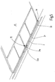
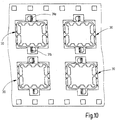
- the Figures 9 and 10 show now a strip with multiple antenna connection frame 30. It can be seen again that each antenna terminal of the frame 30 has two connecting elements 31a, 31b, which in FIG. 10 are shown in enlarged scale.
- FIGS. 8 to 11 now show the preparation of a consisting of the antenna terminal frame 30 and the lead frame 40 support structure 50 for the electronic component 10 'as the microchip 10.
- lead frames 40 are formed, such as a punching, etching or a lamination technique and on a carrier film 51st applied (see FIG. 8 ). The production of such lead frames 40 is known and therefore need not be described in detail.
- FIG. 9 now shows the back of the carrier film 51, on which the connection frame 40 are arranged. It can be seen here, bond openings 41 of the lead frame 40th
- the antenna terminal frame 30 in a likewise known manner by punching, etching, etc. formed of a flat base material.
- FIG. 10 four antenna connection frames 30 each with two connecting elements 31a, 31b.
- the antenna connector frame 30 and the lead frame 40 are connected together, for. B. by an appropriate bond.
- the carrier structure 50 formed in this way is then inserted into the carrier body 2 of the smartcard 1, comparable to the insertion of a conventional leadframe.
- the antenna terminal frame 30 is formed so as to be potting the support structure 50 and the electronic component 10 'received by it with a corresponding resin or the like Medium, so a potting mass, limited the course of this potting mass. This advantageously simplifies the production of an electronic component 10 'using the described smartcard blank.
- Another advantage of the measures described is that it is no longer absolutely necessary to provide rings, in particular copper rings, around the bonding openings 42. The occurrence of a short circuit between inserted into the bonding openings 42 bonding wires and the electronic component 10 'is counteracted thereby.
- the smartcard blank 1 and thus the smartcard 1 formed therefrom has two interfaces for information exchange between the smartcard 1 and the peripheral device using it, namely a first interface for a touch-connected connection and a second interface Interface for a contactless connection. It will be apparent to those skilled in the art that this will provide a smart card having a dual interface arrangement. But this is not mandatory. For certain applications, it may well be sufficient that the smart card 1 has only one interface for a non-contact connection. In this case, the first interface, namely the touch-sensitive interface, can then be omitted.
- a smart card blank 1 'and a method for its production are formed, which significantly simplify the production of a smart card 1 with at least one non-contact interface, since by the in the carrier body 2 of the smartcard blank 1' provided connecting elements 31a, 31b, which are preferably formed as components of an antenna connection frame 30, a direct contact between the inserted into the recess 3 'of the support body 2 electronic component 10', in particular a microchip 10, and the distance to this electronic component 10 'arranged connection elements 22a, 22b of the antenna 20 is made possible, in which by the one or more connecting elements 31a, 31b, the height difference between these two levels is bridged.
Landscapes
- Engineering & Computer Science (AREA)
- Microelectronics & Electronic Packaging (AREA)
- Computer Hardware Design (AREA)
- Physics & Mathematics (AREA)
- General Physics & Mathematics (AREA)
- Theoretical Computer Science (AREA)
- Credit Cards Or The Like (AREA)
- Support Of Aerials (AREA)
Description
- Die Erfindung betrifft einen Smartcard-Rohling mit mindestens einer Schnittstelle zur berührungslosen Übertragung von Informationen, der einen Trägerkörper mit einer Ausnehmung aufweist, in die ein elektronisches Bauteil wie ein Mikrochip einsetzbar ist, wobei im Trägerkörper eine Antenne vorgesehen ist, welche mit dem in die Ausnehmung eingesetzten elektronischen Bauteil elektrisch leitend verbunden ist, wobei die Antenne mindestens ein Anschlußelement zur Herstellung einer elektrisch leitenden Verbindung mit dem elektronischen Bauteil besitzt, welches in einer ersten Ebene im Trägerkörper des Smartcard-Rohlings angeordnet ist, die von einer durch das elektronische Bauteil festgelegten zweiten Ebene beabstandet ist, so dass zwischen dem elektronischen Bauteil und dem Anschlußelement eine Höhendifferenz gegeben ist, sowie eine diesen Smartcard-Rohling verweisende Smartcard und ein Verfahren zu seiner Herstellung.
- Eine derartige Smartcard wird weitverbreitet verwendet. Sie besitzt einen oft Scheckkarten-großen Trägerkörper, der mit einer Ausnehmung versehen ist, in welche ein Mikrochip eingesetzt ist. Dieser Mikrochip weist zur Ausbildung einer ersten Schnittstelle ein berührungsgebundenes Kontaktelement auf oder ist mit einem derartigen Kontaktelement der Smartcard elektrisch leitend verbunden, so dass durch einen mechanischen Kontakt zwischen diesem Kontaktelement und einem korrespondierenden Kontaktelement eines mit der Smartcard zusammenwirkenden Peripheriegeräts ein elektrisch leitender Kontakt zwischen dem Mikrochip der Smartcard und z. B. einem Kartenleser des diese Smartcard verwendenden Peripheriegeräts, z. B. ein Terminal, ein Waren- oder Geldausgabeautomat oder dergleichen hergestellt wird und dieses Peripheriegerät auf die auf dem Mikrochip gespeicherten Daten, Informationen und/oder Programme, insbesondere Anwendungsprogramme, zugreifen kann.
- Moderne Smartcards weisen des weiteren noch als eine zweite Schnittstelle eine elektrisch leitend mit dem Mikrochip verbundene Antenne auf, welche dazu dient, eine berührungslose Verbindung zwischen dem die Smartcard verwendenden Peripheriegerät und dem Mikrochip, etwa durch eine RFID- oder NFC-Technik, herzustellen.
- Zu diesem Zweck muss der in der Ausnehmung des Kartenkörpers aufgenommene Mikrochip mit Anschlußelementen der Antenne verbunden werden. Die Antenne ist in der Regel, die den Mikrochip aufnehmende Ausnehmung umgebend, in einer ersten Ebene des Trägerkörpers angeordneten, die unter einer zweiten, durch den Mikrochip festgelegten Ebene liegt. Es ist daher eine die Höhendifferenz zwischen dem Mikrochip und den Anschlußelementen der Antenne gegeben, die durch eine elektrisch leitende Verbindung überbrückt werden muss.
- Bis jetzt wird - wie z. B. aus der
US 2006/0038022 A1 bekannt - eine derartige Verbindung derart ausgebildet, dass ein elektrisch leitender Kleber eingesetzt wird, um die Verbindung zwischen dem Mikrochip und den Anschlußelementen der Antenne herzustellen. Der Hersteller der fertigen Smartcard bezieht also einen Smartcard-Rohling, in den er dann den mit den entsprechenden Daten und/oder Programmen ausgerüsteten Mikrochip einsetzen muss. Zur Fertigstellung der Smartcard muss er daher nicht nur diesen Chip in die Ausnehmung des Kartenkörpers des Smartcard-Rohlings einsetzen und mit einem den Mikrochip tragenden Leiterrahmen, üblicherweise als Lead-frame bezeichnet, verbinden, sondern muss auch noch in einem weiteren Schritt vor oder gleichzeitig mit dem Einsetzen des Mikrochips in die Ausnehmung den elektrisch leitenden Kleber applizieren, um die vorstehend beschriebene elektrisch leitende Verbindung zwischen dem Mikrochip und der im Smartcard-Rohling vorgesehenen Antenne herzustellen. - Aus der
DE 197 49 650 A1 ist eine Chipkarte und ein Verfahren zur Herstellung einer elektronischen Verbindung eines in eine Kavität eines Kartenkörpers der Chipkarte eingesetzten Moduls, welches eine elektronische Komponente aufweist, bekannt. Die Chipkarte weist einen Kartenkörper, eine aus diesem herausgearbeitete Kavität, einen Chip oder ein anderes elektronische Komponenten enthaltendes Modul mit Antennenanschlusskontakten auf, welche zur Verbindung mit einer Antenne oder einer Antennenschicht mit Antenneneinrichtungen im Kartenkörper dienen, wobei der Kartenkörper Kontakte zum Anschließen des Chips aufweist. Es ist vorgesehen, dass zwischen den Kontakten im Kartenkörper und den Antennenanschlusskontakten, diese leitend verbindend, ein Kontaktelement vorgesehen ist, welches die Kontakte und die Antennenanschlusskontakte elektrisch leitend verbinden. Es kann hierzu auch ein leitfähiger metallischer Bolzen angeordnet sein. - Aus der
EP 2 290 590 A2 ist ein portabler Datenträger bekannt, der einen Datenträgerkörper mit einer elektronischen Komponente sowie ein elektronisches Modul besitzt. Dieses Ist zumindest teilweise in den Datenträgerkörper eingebettet und über eine Modulkontakteinrichtung des Moduls mittels eines elastischen, elektrisch leitfähigen Materials unter Druckbeaufschlagung elektrisch leitend mit einer Komponentenkontakteinrichtung der elektronischen Komponente des Datenträgers verbunden. Die Modulkontakteinrichtung ist räumlich strukturiert ausgebildet und in das elastische, elektrisch leitfähige Material durch die räumlich strukturierte Modulkontakteinrichtung ist eine räumliche Struktur eingeprägt. - Es ist daher Aufgabe der vorliegenden Erfindung, einen Smartcard-Rohling der eingangs genannten Art sowie ein Verfahren zu seiner Herstellung derart weiterzubilden, dass dessen Fertigstellung zu einer funktionsfähigen Smartcard vereinfacht ist.
- Diese Aufgabe wird erfindungsgemäß dadurch gelöst, dass im Smartcard-Rohling mindestens ein Verbindungselement zur Herstellung einer elektrisch leitenden Verbindung mit dem Leiterrahmen vorgesehen ist, welches sich zwischen der vorgenannten ersten Ebene und der vorgenannten zweiten Ebene erstreckt, und wobei dieses mindestens eine Verbindungselement eine Höhe aufweist, die im Wesentlichen gleich der Höhendifferenz zwischen den beiden vorgenannten Ebenen ist, und dass das mindestens eine Verbindungselement Teil des Antennenanschlußrahmens ist.
- Das erfindungsgemäße Verfahren sieht vor, dass durch ein in einen Trägerkörper des Smartcard-Rohlings angeordnetes Verbindungselement eine Höhendifferenz zwischen einer durch ein einem Anschlußelement einer Antenne festgelegten erster Ebene und einer durch das elektronische Bauteil festgelegten zweiten Ebene überbrückt wird.
- Durch die erfindungsgemäßen Maßnahmen wird in vorgenannter Art und Weise ein Smartcard-Rohling für eine Smartcard sowie ein Verfahren zu seiner Herstellung geschaffen, welche sich dadurch auszeichnen, dass die Montage des in diesen Smartcard-Rohling einzusetzenden elektronischen Bauteils vereinfacht ist, da zur Verbindung dieses elektronischen Bauteils mit der im Trägerkörper der Smartcard-Rohlings angeordneten Antenne kein externes Verbindungsmittel wie ein elektrisch leitfähiger Kleber oder dergleichen eingesetzt werden muss. Da das erfindungsgemäß im Smartcard-Rohling vorgesehene Verbindungselement zur Überbrückung der Höhendifferenz zwischen der Antenne und dem elektronischen Bauteil besitzt den Vorteil, dass die Kontaktierung des in den Smartcard-Rohling eingesetzten elektronischen Bauteils, insbesondere eines Mikrochips, mit der Antenne besonders einfach durchzuführen ist.
- Eine vorteilhafte Weiterbildung der Erfindung sieht vor, dass das erfindungsgemäße Verbindungselement als eine Zunge oder zungenartig ausgebildet ist und einen aus dem Grundkörper dieses Verbindungselement vorstehenden Bereich aufweist, dessen Höhe im Wesentlichen gleich der Höhendifferenz zwischen der ersten Ebene, die durch das oder die Anschlusselemente der Antenne festgelegt ist, und der zweiten Ebene, die durch das elektronische Bauteil festgelegt ist, beträgt. Der Vorsprung kann insbesondere durch ein entsprechendes Biegen und/oder Prägen des Verbindungselements oder durch Vorsehen einer wellenförmigen und/oder kugelförmigen Struktur ausgebildet wird. Eine derartige Maßnahme bewirkt, dass das erfindungsgemäße Verbindungselement besonders leicht und einfach herstellbar ist.
- Die Erfindung sieht vor, dass das oder zumindest eines der Verbindungselemente Teil eines Antennenanschlussrahmens ist, der im erfindungsgemäßen Smartcard-Rohling vorgesehen ist. Hierdurch wird wiederum eine besonders einfache Herstellbarkeit ermöglicht.
- Eine weitere vorteilhafte Weiterbildung der Erfindung sieht vor, dass der Anschlussrahmen und ein das elektronische Bauteil tragender Leiterrahmen miteinander verbunden sind. Diese Maßnahme hat den Vorteil, dass hierdurch der Antennenrahmen zusammen mit dem Leiterrahmen einfach in den Trägerkörper des Smartcard-Rohlings eingesetzt ist.
- Eine weitere vorteilhafte Weiterbildung der Erfindung sieht vor, dass der Smartcard-Rohling eine weitere Schnittstelle aufweist, durch die eine berührungsgebundene Kontaktierung des elektronischen Bauteils ermöglicht ist. Eine derartige Maßnahme besitzt den Vorteil, dass hierdurch eine duale Kontaktierung des elektronischen Bauteils ausgebildet wird, sodass die den erfindungsgemäßen Smartcard-Rohling verwendende Smartcard sowohl berührungslos als auch berührungsgebunden mit einem diese Smartcard verwendende Peripheriegerät kommunizieren kann.
- Weitere vorteilhafte Weiterbildungen der Erfindung sind Gegenstand der Unteransprüche.
- Weitere Einzelheiten und Vorteile der Erfindung sind dem Ausführungsbeispiel zu entnehmen, das im Folgenden anhand der Figuren beschrieben wird. Es zeigen:
- Figur 1
- eine schematische Darstellung einer Smartcard,
- Figur 2
- systematische Darstellung eines Ausführungsbeispiels eines Smart-card-Rohlings, wobei dessen Deckfläche durchsichtig gezeigt ist,
- Figur 3
- eine vergrößerte Darstellung einer Ausnehmung des Trägerkörpers des Smartcard-Rohlings,
- Figur 4
- eine vergrößerte Darstellung des Teilbereichs IV der
Figur 3 , - Figur 5
- einen Querschnitt (auszugsweise) durch das Ausführungsbeispiel,
- Figur 6
- einen Ausschnitt aus dem Querschnitt der
Figur 5 , - Figur 7
- eine Darstellung eines Verbindungselements,
- Figuren 8-11
- eine schematische Darstellung der Herstellung einer Trägerstruktur für ein elektronisches Bauteil aus einem Antennenanschlussrahmen und einen Leiterrahmen.
- In
Figur 1 ist ein Ausführungsbeispiel einer allgemein mit 1 bezeichneten Smartcard dargestellt. Die Smartcard 1 gliedert sich grundsätzlich in einen Smartcard-Rohling 1', der eine Ausnehmung 3 aufweist, in der in an und für sich bekannter und daher nicht mehr näher beschriebenen Art und Weise ein elektronisches Bauteil 10', wie z. B. einen Mikrochip 10, aufgenommen ist. Das elektronische Bauteil 10' wird von einem Leiterrahmen 40 (siehe dazuFigur 2 ) getragen, welcher elektrisch leitend mit diesem verbunden ist. - Der Smartcard-Rohling 1' weist in einer an und für sich ebenfalls bekannten und daher nicht mehr näher beschriebene Art und Weise einen Trägerkörper 2 auf, in dem die Ausnehmung 3 vorgesehen ist, in die das in der
Figur 1 nur schematisch dargestellte elektronische Bauteil 10' wie z. B. der in dieser Figur dargestellte Mikrochip 10 eingesetzt ist. Dieser weist an seiner ersten Oberfläche 11a eine Anzahl von Kontaktelementen 12 auf. Diese dienen zur Herstellung einer elektrisch leitenden Verbindung zwischen einem die beschriebene Smartcard 1 verwendenden Peripheriegerät, wie z. B. einem Kartenleser oder einem Terminal oder einer Ausgabevorrichtung wie einem Verkaufsautomaten oder einem Geldausgabeautomaten, und dem Mikrochip 10 der Smartcard 1, die durch einen mechanischen Kontakt zwischen den Kontaktelementen 12 des Mikrochips 10 und korrespondierenden Kontaktelementen des Peripheriegeräts hergestellt wird. Über die Kontaktelemente 12 des Mikrochips 10 ist es somit diesem Peripheriegerät möglich, auf die im Mikrochip 10 gespeicherten Informationen wie Daten und/oder Programme zuzugreifen. Die Kontaktelemente 12 bilden somit eine erste, berührungsgebundene Schnittstelle für einen Informationsaustausch zwischen dem elektronischen Bauteil 10', hier also dem Mikrochip 10, und dem Peripheriegerät aus. Im Sinne einer prägnanteren Beschreibung soll unter dem Begriff "Informationen" sowohl Daten als auch Programme, insbesondere Anwendungsprogramme, die auf dem elektronischen Bauteil 10', insbesondere dem Mikrochip 10 implementiert oder gespeichert sind, verstanden werden. Des weiteren wird im folgenden anstelle von einem elektronischen Bauteil 10' von einem Mikrochip 10 gesprochen, wobei aber dieser Mikrochip 10 nur als Beispiel für ein elektronisches Bauteil 10' gemeint ist. Ein derartiger Aufbau einer Smartcard 1 sowie die Herstellung derselben aus einem Smartcard-Rohling 1 durch Einsetzen eines elektronischen Bauteils 10' in die Ausnehmung 3 und eine entsprechende Kontaktierung des elektronischen Bauteils 10' mit dem Leiterrahmen 40 ist bekannt und muss daher nicht mehr näher beschrieben werden. - Die
Figur 2 zeigt nun den Smartcard-Rohling derFigur 1 , wobei in der Darstellung derFigur 2 die Oberfläche des Smartcard-Rohlings 1' durchsichtig dargestellt ist, sodass dessen prinzipieller innerer Aufbau aus dieser Figur ersichtlich ist. Nicht gezeigt ist der inFigur 1 ersichtliche Mikrochip 10, so dass aus derFigur 2 der unter dem Mikrochip 10 angeordnete, diesen tragende Leiterrahmen 40 ersichtlich ist. - Um nun auch eine berührungslose Kontaktierung der Smartcard 1 zu ermöglichen, ist im Trägerkörper 2 des Smartcard-Rohlings 1' eine Antenne 20 angeordnet, die in einem elektrisch leitenden Kontakt mit dem in die Ausnehmung 3 eingesetzte Mikrochip 10 steht, so dass ein entsprechend ausgestattetes Peripheriegerät mit dem Mikrochip 10 durch eine berührungslose Übertragungstechnik, z. B. durch eine RFID-Technik oder eine NFC-Technik, über diese zweite Schnittstelle der Smartcard 1 auf den Mikrochip 10 zugreifen kann. Die Antenne 20 besitzt Antennendrähte 21, die zur Ausnehmung 3 hinführen und zumindest in einem Bereich unter dieser verlaufen. Auch ein derartiger Smartcard-Rohling 1 sowie eine diesen verwendende Smartcard 1 mit einer dualen Schnittstelle sind bekannt und müssen daher nicht mehr weiter im Detail beschrieben werden.
- Die
Figur 3 zeigt nun den Bereich der Ausnehmung 3 der Smartcard 1 derFigur 2 in einer vergrößerten Darstellung und dieFigur 4 eine vergrößerte Darstellung des Bereichs II derFigur 3 , jeweils aber ohne den inFigur 1 dargestellten Mikrochip 10 sowie den diesen tragenden, Leiterrahmen 40, wobei der übersichtlichen Darstellung halber die Antenne 20 außerhalb des Bereichs der Ausnehmung 3 ebenfalls nicht gezeigt ist. Man erkennt somit einen im montierten Zustand unter den Leiterrahmen 40 liegenden Antennenanschlussrahmen 30, welcher - wie nachstehend beschrieben - zur elektrischen Kontaktierung des Mikrochips 10, also allgemein des elektronischen Bauteils 10', mit der Antenne 20 dient. Ebenfalls erkennt man aus derFigur 3 , dass ein Boden 3' der Ausnehmung 3 zwei Durchtrittsöffnungen 3a und 3b besitzt, unter denen Drähte 21 der Antenne 20 verlaufen. Dies ist insbesondere aus derFigur 4 ersichtlich. Die unter den Durchtrittsöffnungen 3a und 3b der Ausnehmung 3 des Trägerkörpers 2 liegenden Drähte 21 bilden Anschlußelemente 22a, 22b der Antenne 20 aus, über welche die Antenne 20 - wie nachstehend beschrieben - mit dem (später) in die Ausnehmung 3 eingesetzten Mikrochip 10 elektrisch leitend verbunden werden kann. Man erkennt des weiteren aus denFiguren 3 und4 , dass die Drähte 21 die Antenne 20 von den Verbindungselementen 31a, 31b des Antennenanschlußrahmens 30 beaufschlagt werden, welcher mit dem Mikrochip 10 in elektrisch leitendem Kontakt steht. - Die
Figur 5 zeigt nun - auszugsweise - einen Querschnitt durch das Ausführungsbeispiel und dieFigur 6 ist eine vergrößerte Darstellung des Bereichs VI derFigur 5 . Man erkennt den Trägerkörper 2 des Smartcard-Rohlings 1 sowie den Antennenanschlußrahmen 30 und den Leiterrahmen 40. Ebenfalls ersichtlich sind die Drähte 21 der Antenne 20, die in einer ersten Ebene, einer "Antennenebene", des Trägerkörpers 2 angeordnet sind. Üblicherweise liegen alle Drähte 21 der Antenne 20 in dieser ersten Ebene. Dies ist aber nicht zwingend erforderlich. Ausreichend ist, dass der Bereich der Drähte 21, welche die Anschlußelemente 22a und 22b ausbilden, also unter den Öffnungen 3a und 3b der Ausnehmung 3 liegen, in dieser ersten Ebene liegen. - Insbesondere aus
Figur 6 ist ersichtlich, dass diese erste Ebene von einer durch den Mikrochip 10 bzw. den diesen tragenden Leiterrahmen 40 festgelegten zweiten Ebene des Trägerkörpers 2 beabstandet angeordnet ist. Im hier beschriebenen Ausführungsbeispiel wird diese Höhendifferenz zwischen diesen beiden Ebenen durch die Verbindungselemente 31a und 31b des Antennenanschlußrahmens 30 überbrückt, so dass eine elektrisch leitende Verbindung zwischen dem Antennenanschlußrahmen 30, der elektrisch leitend mit dem Mikrochip 10 verbunden ist, und der Antenne 20 hergestellt ist. Hierdurch wird die dem berührungslosen Informationsaustausch dienende Schnittstelle der Smartcard 1 hergestellt. Der Antennenanschlußrahmen 30 ist also bereits im Smartcard-Rohling 1' angeordnet, so dass der diesen Smartcard-Rohling 1' zur Herstellung einer fertigen Smartcard 1 verwendende Smartcard-Hersteller lediglich das elektronische Bauteil 10', hier also den Mikrochip 10, in die Ausnehmung 3 einzusetzen und in bekannter Weise mit dem Leiterrahmen 40 elektrisch leitend verbinden muss, z. B. durch Bonden, um aus dem Smartcard-Rohling 1' und dem elektronischen Bauteil 10 eine funktionsfähige Smartcard 1 herzustellen. Das bisher übliche Applizieren eines leitfähigen Klebers beim Einsetzen eines Mikrochips 10 in einen Smartcard-Rohling 1' zur Herstellung einer elektrisch leitenden Verbindung zwischen diesem elektronischen Bauteil 10' und der Antenne 20 entfällt somit, wodurch die Herstellung einer Smartcard 1 deutlich vereinfacht wird. - Wie aus den Figuren ersichtlich ist, ist im hier beschriebenen Fall vorgesehen, dass die Verbindungselemente 31a und 31b als eine aus der Ebene des Antennenanschlußrahmens 30 hervorstehende Zungen 31 ausgebildet sind, die einen Vorsprung 33 besitzen, so dass durch diesen Vorsprung 33 die Höhendifferenz zwischen der durch die Antennenanschlußelemente 22a, 22b festgelegten ersten Ebene und der zweiten Ebene des Mikrochips 10 überbrückt ist und die Verbindungselemente 31a, 31b in elektrisch leitenden Kontakt mit den Anschlußelementen 22a, 22b treten können.
- Bevorzugt wird, dass - wie am besten aus
Figur 7 ersichtlich - die Verbindungselemente 31a und 31b jeweils einen Grundkörper 32 mit einem gebogenen, vorzugsweise höckerartigen Verlauf aufweisen, so dass der aus der Ebene des Antennenanschlußrahmens 30 hervortretender höckerartige Vorsprung 33 sich zu den Anschlußelementen 22a bis 22b der Antenne 20 hin erstreckt und mit diesen elektrisch leitend in Kontakt tritt. Eine derartige zungenartige Ausgestaltung ist aber nicht zwingend erforderlich. Auch eine wellen- und/oder kugelförmige Ausgestaltung der Verbindungselemente 31a, 31b ist möglich, genauso wie das Vorsehen einer Prägung. Grundsätzlich ist jede Ausgestaltung der Verbindungselemente 31a, 31b möglich, durch welche eine Überbrückung der Höhendifferenz zwischen der durch die Anschlußelemente 22a, 22b der Antenne 20, also die unter den Durchtrittsöffnungen 3a, 3b verlaufenden Drähte 21, festgelegten ersten Ebene und der durch den Leiterrahmen 40 festgelegten zweiten Ebene überbrückt wird. Bevorzugt wird jedoch die vorstehend beschriebene Ausgestaltung der Verbindungselemente 31a, 31b, wobei des weiteren bevorzugt wird, dass diese Verbindungselemente 31a, 31b federnd ausgebildet sind. Hierdurch können Fertigungstoleranzen einfach ausgeglichen werden. - Die
Figur 7 zeigt die Kontaktseite des Leiterrahmens 40, auf der Anschlussfelder 41 vorgesehen sind, die zur elektrisch leitenden Verbindung des Leiterrahmens 40 zu dem elektronischen Bauteil 10', also hier mit dem Mikrochip 10, dienen. DieFigur 8 zeigt die Rückseite des Leiterrahmens 40. Man erkennt Bondöffnungen 42. DieFiguren 9 und10 zeigen nun einen Streifen mit mehreren Antennenanschlussrahmen 30. Man erkennt wiederum, dass jeder Antennenanschluss des Rahmens 30 zwei Verbindungselemente 31a, 31b besitzt, welche inFigur 10 in vergrößertem Maßstab dargestellt sind. - Die
Figuren 8 bis 11 zeigen nun die Herstellung einer aus dem Antennenanschlußrahmen 30 und dem Leiterrahmen 40 bestehenden Trägerstruktur 50 für das elektronische Bauteil 10' wie dem Mikrochip 10. Hierzu werden Anschlußrahmen 40 ausgebildet, etwa durch eine Stanz-, eine Ätz- oder eine Laminiertechnik und auf eine Trägerfolie 51 aufgebracht (sieheFigur 8 ). Die Herstellung derartiger Leiterrahmen 40 ist bekannt und muss daher nicht mehr näher beschrieben werden. - Die
Figur 9 zeigt nun die Rückseite der Trägerfolie 51, auf der die Anschlussrahmen 40 angeordnet sind. Man erkennt hier Bondöffnungen 41 des Leiterrahmens 40. - Der Antennenanschlußrahmen 30 in ebenfalls bekannter Art und Weise durch Stanzen, Ätzen, etc. aus einem flachen Grundmaterial ausgebildet. Man erkennt aus
Figur 10 vier Antennenanschlußrahmen 30 mit jeweils zwei Verbindungselementen 31a, 31b. - Wie aus der
Figur 11 ersichtlich, werden dann der Antennenanschlußrahmen 30 und der Leiterrahmen 40 miteinander verbunden, z. B. durch eine entsprechende Verklebung. Die derartig gebildete Trägerstruktur 50 wird dann - vergleichbar mit dem Einsetzen eines konventionellen Leiterrahmens - in den Trägerkörper 2 der Smartcard 1 eingesetzt. - Vorzugsweise ist der Antennenanschlußrahmen 30 derart ausgebildet, dass er beim Umhüllen ("potting") der Trägerstruktur 50 und des von ihr aufgenommenen elektronischen Bauteils 10' mit einem entsprechenden Harz oder einem ähnlichen Mittel, also einer Potting-Masse, den Verlauf dieser Potting-Masse begrenzt. Dies vereinfacht in vorteilhafter Art und Weise die Herstellung eines den beschriebenen Smartcard-Rohling verwendenden elektronischen Bauteils 10'.
- Ein weiterer Vorteil der beschriebenen Maßnahmen ist, dass es nicht mehr zwingend erforderlich ist, Ringe, insbesondere Kupferringe, um die Bondöffnungen 42 vorzusehen. Dem Auftreten eines Kurzschlusses zwischen in die Bondöffnungen 42 eingeführten Bonddrähten und dem elektronischen Bauteil 10' wird hierdurch entgegengewirkt.
- Bei der bevorstehenden Beschreibung wird davon ausgegangen, dass der Smartcard-Rohling 1' und somit die aus ihm ausgebildete Smartcard 1 zwei Schnittstellen für einen Informationsaustausch zwischen der Smartcard 1 und dem diese verwendende Peripheriegerät besitzt, nämlich eine erste Schnittstelle für eine berührungsgebundene Verbindung und eine zweite Schnittstelle für eine berührungslose Verbindung. Dem Fachmann ist ersichtlich, dass hierdurch eine Smartcard mit einer dualen Schnittstellenanordnung ausgebildet wird. Dies ist aber nicht zwingend erforderlich. Für bestimmte Anwendungszwecke kann es durchaus ausreichend sein, dass die Smartcard 1 nur eine Schnittstelle für eine berührungslose Verbindung besitzt. In diesem Fall kann dann die erste Schnittstelle, nämlich die berührungsgebundene Schnittstelle, entfallen.
- Zusammenfassend ist festzuhalten, dass durch die beschriebenen Maßnahmen ein Smartcard-Rohling 1' sowie ein Verfahren zu seiner Herstellung ausgebildet werden, welche die Herstellung einer Smartcard 1 mit zumindest einer berührungslosen Schnittstelle deutlich vereinfachen, da durch die im Trägerkörper 2 des Smartcard-Rohlings 1' vorgesehenen Verbindungselemente 31a, 31b, die vorzugsweise als Bestandteile eines Antennenanschlußrahmens 30 ausgebildet sind, eine direkte Kontaktierung zwischen dem in die Ausnehmung 3' des Trägerkörpers 2 eingesetzten elektronischen Bauteil 10', insbesondere einem Mikrochip 10, und dem beabstandet zu diesem elektronischen Bauteil 10' angeordneten Anschlußelementen 22a, 22b der Antenne 20 ermöglicht wird, in dem durch das oder die Verbindungselemente 31a, 31b die zwischen diesen beiden Ebenen gegebene Höhendifferenz überbrückt wird.
Claims (9)
- Smartcard-Rohling mit mindestens einer Schnittstelle zur berührungslosen Übertragung von Informationen, der einen Trägerkörper (2) mit einer Ausnehmung (3) aufweist, in die ein elektronisches Bauteil (10') wie ein Mikrochip (10) einsetzbar ist, wobei der Smartcard-Rohling (1) einen Leiterrahmen (40) besitzt, durch den das in die Ausnehmung (3) des Trägerkörpers (2) einzusetzende elektronische Bauteil (10') elektrisch kontaktierbar ist, wobei im Trägerkörper (2) eine Antenne (20) vorgesehen ist, welche mit dem in die Ausnehmung (3) eingesetzten elektronischen Bauteil elektrisch leitend verbunden ist, wobei die Antenne (20) einen Antennenanschlußrahmen mit mindestens einem Anschlußelement (22a, 22b) zur Herstellung einer elektrisch leitenden Verbindung mit dem elektronischen Bauteil (10') besitzt, wobei das Anschlußelement (22a, 22b) in einer ersten Ebene im Trägerkörper (2) des Smartcard-Rohlings (1') angeordnet ist, welche von einer durch den das elektronische Bauteil (10') tragenden Leiterrahmen (40) festgelegten zweiten Ebene beabstandet ist, so dass zwischen diesen beiden Ebenen eine Höhendifferenz gegeben ist, dadurch gekennzeichnet, dass im Smartcard-Rohling (1) mindestens ein Verbindungselement (31a; 31b) zur Herstellung einer elektrisch leitenden Verbindung mit dem Leiterrahmen (40) vorgesehen ist, welches sich zwischen der vorgenannten ersten Ebene und der vorgenannten zweiten Ebene erstreckt, und wobei dieses mindestens eine Verbindungselement (31a; 31b) eine Höhe aufweist, die im Wesentlichen gleich der Höhendifferenz zwischen den beiden vorgenannten Ebenen ist, und dass das mindestens eine Verbindungselement (31a; 31b) Teil des Antennenanschlußrahmens (30) ist.
- Smartcard-Rohling nach Anspruch 1, dadurch gekennzeichnet, dass mindestens ein Verbindungselement (31a, 31b) als eine Zunge oder zungenartig ausgebildet ist und einen Vorsprung (33) besitzt.
- Smartcard-Rohling nach einem der vorangehenden Ansprüche, dadurch gekennzeichnet, dass mindestens ein Verbindungselement (31a, 31b) wellen- und/oder kugelförmig oder als Prägung ausgestaltet ist.
- Smartcard-Rohling nach einem der vorangehenden Ansprüche, dadurch gekennzeichnet, dass die Ausnehmung (3) des Trägerkörpers (2) mindestens eine Durchtrittsöffnung (3a; 3b) für ein Verbindungselement (31a; 31b) besitzt.
- Smartcard-Rohling nach einem der vorangehenden Ansprüche, dadurch gekennzeichnet, dass der Leiterrahmen (40) und der Antennenanschlußrahmen (30) miteinander zu einer Trägerstruktur verbunden sind.
- Smartcard-Rohling nach einem der vorangehenden Ansprüche, dadurch gekennzeichnet, dass der Smartcard-Rohling (1) mindestens ein berührungsgebundenes Kontaktelement (21) aufweist,
- Smartcard, die einen Smartcard-Rohling (1) sowie ein in dessen Ausnehmung (3) einzusetzendes elektronisches Bauteil (10') aufweist, dadurch gekennzeichnet, dass der Smartcard-Rohling (1) nach einem der Ansprüche 1 bis 6 ausgebildet ist.
- Verfahren zur Herstellung eines Smartcard-Rohlings (1') gemäß einem der Ansprüche 1 bis 6, dadurch gekennzeichnet, dass durch ein in einen Trägerkörper (2) des Smartcard-Rohlings (1') angeordnetes Verbindungselement (31a; 31b) eine Höhendifferenz zwischen einer durch ein das oder die Anschlußelemente (22a; 22b) einer Antenne (20) festgelegten ersten Ebene und einer durch einen das elektronische Bauteil (10') tragenden Leiterrahmen (40) festgelegten zweiten Ebene überbrückt wird.
- Verfahren zur Herstellung einer Smartcard (1) aus einem Smartcard-Rohling (1') und einem elektronischen Bauteil (10'), wobei der Smartcard-Rohling (1') eine Ausnehmung (3) aufweist, in welche das elektronische Bauteil (10') einsetzbar ist, dadurch gekennzeichnet, dass zur Herstellung der Smartcard (1) ein Smartcard-Rohling (1') nach einem der Ansprüche 1 bis 6 verwendet wird.
Applications Claiming Priority (3)
| Application Number | Priority Date | Filing Date | Title |
|---|---|---|---|
| DE102015007970.0A DE102015007970A1 (de) | 2015-06-23 | 2015-06-23 | Smartcard-Rohling mit mindestens einer Schnittstelle zur berührungslosen Übertragung von Informationen |
| DE202015004427.1U DE202015004427U1 (de) | 2015-06-23 | 2015-06-23 | Smartcard-Rohling mit mindestens einer Schnittstelle zur berührungslosen Übertragung von Informationen |
| PCT/EP2016/001059 WO2016206801A1 (de) | 2015-06-23 | 2016-06-22 | Smartcard-rohling mit mindestens einer schnittstelle zur berührungslosen übertragung von informationen |
Publications (2)
| Publication Number | Publication Date |
|---|---|
| EP3317821A1 EP3317821A1 (de) | 2018-05-09 |
| EP3317821B1 true EP3317821B1 (de) | 2019-07-17 |
Family
ID=56842775
Family Applications (1)
| Application Number | Title | Priority Date | Filing Date |
|---|---|---|---|
| EP16757822.8A Active EP3317821B1 (de) | 2015-06-23 | 2016-06-22 | Smartcard-rohling mit mindestens einer schnittstelle zur berührungslosen übertragung von informationen |
Country Status (6)
| Country | Link |
|---|---|
| EP (1) | EP3317821B1 (de) |
| KR (1) | KR102251694B1 (de) |
| CN (1) | CN107912065B (de) |
| MY (1) | MY186313A (de) |
| SG (1) | SG11201710090YA (de) |
| WO (1) | WO2016206801A1 (de) |
Families Citing this family (1)
| Publication number | Priority date | Publication date | Assignee | Title |
|---|---|---|---|---|
| EP3832547A1 (de) * | 2019-12-02 | 2021-06-09 | Thales Dis France Sa | Die erfindung betrifft ein herstellungsverfahren einer funkfrequenz-chipkarte, die eine metallplatte mit einem schlitz in der platte umfasst |
Family Cites Families (13)
| Publication number | Priority date | Publication date | Assignee | Title |
|---|---|---|---|---|
| DE4431754C1 (de) * | 1994-09-06 | 1995-11-23 | Siemens Ag | Trägerelement |
| ES2149000T3 (es) * | 1996-08-02 | 2000-10-16 | Schlumberger Systems & Service | Tarjeta de circuito integrado con conexion mixta. |
| DE19749650C2 (de) * | 1997-11-10 | 2000-01-13 | Meinen Ziegel & Co Gmbh | Verfahren zum Herstellen einer elektrischen Verbindung eines in einer Kavität eines Kartenkörpers einer Chipkarte eingesetzten, elektronische Komponenten aufweisenden Moduls |
| FR2788646B1 (fr) * | 1999-01-19 | 2007-02-09 | Bull Cp8 | Carte a puce munie d'une antenne en boucle, et micromodule associe |
| DE10257111B4 (de) * | 2002-12-05 | 2005-12-22 | Mühlbauer Ag | Chipkarte und Verfahren zur Herstellung einer Chipkarte |
| KR20070042792A (ko) * | 2005-10-19 | 2007-04-24 | 케이비 테크놀러지 (주) | Usb 데이터 통신 및 비접촉 통신이 가능한 스마트 카드및 스마트 카드 소켓 |
| US8437141B2 (en) * | 2005-11-28 | 2013-05-07 | Nxp B.V. | Device comprising a substrate including an electronic contact, and transponder |
| HK1109708A2 (zh) * | 2007-04-24 | 2008-06-13 | On Track Innovations Ltd. | 介面卡及仪器以及其形成工艺 |
| DE102009037627A1 (de) * | 2009-08-14 | 2011-02-17 | Giesecke & Devrient Gmbh | Portabler Datenträger |
| EP2293228A1 (de) * | 2009-08-28 | 2011-03-09 | Gemalto SA | Herstellungsverfahren für eine Vorrichtung mit einer RFID-Schaltung, entsprechende Vorrichtung und Modul für die Realisierung des Verfahrens |
| KR20120013838A (ko) * | 2010-08-06 | 2012-02-15 | 삼성전기주식회사 | 안테나 패턴이 케이스에 매립되는 전자장치 및 그 제조방법 |
| KR101767720B1 (ko) * | 2012-04-26 | 2017-08-23 | 프리테마 게엠베하 | 반도체 칩을 수용하는 스마트 카드 바디 및 그 제조 방법 |
| DE102012211546B4 (de) * | 2012-07-03 | 2017-02-16 | Morpho Cards Gmbh | Chipkarte mit bei Raumtemperatur pastenförmiger oder flüssiger Kontaktierung |
-
2016
- 2016-06-22 EP EP16757822.8A patent/EP3317821B1/de active Active
- 2016-06-22 CN CN201680036849.1A patent/CN107912065B/zh active Active
- 2016-06-22 KR KR1020187001334A patent/KR102251694B1/ko active Active
- 2016-06-22 WO PCT/EP2016/001059 patent/WO2016206801A1/de not_active Ceased
- 2016-06-22 MY MYPI2017001886A patent/MY186313A/en unknown
- 2016-06-22 SG SG11201710090YA patent/SG11201710090YA/en unknown
Non-Patent Citations (1)
| Title |
|---|
| None * |
Also Published As
| Publication number | Publication date |
|---|---|
| WO2016206801A1 (de) | 2016-12-29 |
| MY186313A (en) | 2021-07-08 |
| EP3317821A1 (de) | 2018-05-09 |
| CN107912065A (zh) | 2018-04-13 |
| SG11201710090YA (en) | 2018-01-30 |
| KR102251694B1 (ko) | 2021-05-13 |
| KR20180019666A (ko) | 2018-02-26 |
| CN107912065B (zh) | 2020-11-03 |
Similar Documents
| Publication | Publication Date | Title |
|---|---|---|
| DE19500925C2 (de) | Verfahren zur Herstellung einer kontaktlosen Chipkarte | |
| EP0931295B1 (de) | Verfahren und verbindungsanordnung zum herstellen einer chipkarte | |
| DE69808112T2 (de) | Herstellungsverfahren einer karte mit gewickelter antenne | |
| WO1998028709A1 (de) | Nicht-leitendes, ein band oder einen nutzen bildendes substrat, auf dem eine vielzahl von trägerelementen ausgebildet ist | |
| WO2009127395A1 (de) | Chipkarte und verfahren zu deren herstellung | |
| DE102014018393A1 (de) | Chipkartenmodul-Anordnung, Chipkarten-Anordnung und Verfahren zum Herstellen einer Chipkarten-Anordnung | |
| AT1470U1 (de) | Laminierte karte und verfahren zu ihrer herstellung | |
| EP2637129B1 (de) | Verfahren zum Freilegen einer Kontaktierungseinrichtung einer elektrischen Komponente in einem portablen Datenträger | |
| DE10108080C1 (de) | Kontaktlos arbeitender Datenträger mit einer kapazitiv an das Modul gekoppelten Antennenspule | |
| WO1998048379A1 (de) | Chipkarte und verfahren zur herstellung einer chipkarte | |
| EP3317821A1 (de) | Smartcard-rohling mit mindestens einer schnittstelle zur berührungslosen übertragung von informationen | |
| WO2008138531A1 (de) | Kontaktloses übertragungssystem und verfahren zum herstellen desselben | |
| DE19749650C2 (de) | Verfahren zum Herstellen einer elektrischen Verbindung eines in einer Kavität eines Kartenkörpers einer Chipkarte eingesetzten, elektronische Komponenten aufweisenden Moduls | |
| DE102020122437A1 (de) | Package, Verfahren zum Bilden eines Packages, Trägerband, Chipkarte und Verfahren zum Bilden eines Trägerbands | |
| EP4315161B1 (de) | Chipkarte und verfahren zur herstellung einer chipkarte | |
| DE202015004427U1 (de) | Smartcard-Rohling mit mindestens einer Schnittstelle zur berührungslosen Übertragung von Informationen | |
| DE102015007970A1 (de) | Smartcard-Rohling mit mindestens einer Schnittstelle zur berührungslosen Übertragung von Informationen | |
| EP2290590B1 (de) | Portabler Datenträger | |
| DE102005002732A1 (de) | Tragbarer Datenträger | |
| DE10210606A1 (de) | Tragbarer Datenträger mit Displaymodul und Verfahren zu seiner Herstellung | |
| EP2045763B1 (de) | Verfahren zum Herstellen von Datenträgern, Vorrichtung zum Durchführen des Verfahrens sowie Vorprodukt zum Herstellen von Datenträgern | |
| DE102005002733B4 (de) | Tragbarer Datenträger | |
| EP1610261B1 (de) | Chipmodul für einen tragbaren Datenträger | |
| DE102005002731A1 (de) | Tragbarer Datenträger | |
| DE102005002728A1 (de) | Tragbarer Datenträger |
Legal Events
| Date | Code | Title | Description |
|---|---|---|---|
| STAA | Information on the status of an ep patent application or granted ep patent |
Free format text: STATUS: THE INTERNATIONAL PUBLICATION HAS BEEN MADE |
|
| PUAI | Public reference made under article 153(3) epc to a published international application that has entered the european phase |
Free format text: ORIGINAL CODE: 0009012 |
|
| STAA | Information on the status of an ep patent application or granted ep patent |
Free format text: STATUS: REQUEST FOR EXAMINATION WAS MADE |
|
| 17P | Request for examination filed |
Effective date: 20180110 |
|
| AK | Designated contracting states |
Kind code of ref document: A1 Designated state(s): AL AT BE BG CH CY CZ DE DK EE ES FI FR GB GR HR HU IE IS IT LI LT LU LV MC MK MT NL NO PL PT RO RS SE SI SK SM TR |
|
| AX | Request for extension of the european patent |
Extension state: BA ME |
|
| DAV | Request for validation of the european patent (deleted) | ||
| DAX | Request for extension of the european patent (deleted) | ||
| GRAP | Despatch of communication of intention to grant a patent |
Free format text: ORIGINAL CODE: EPIDOSNIGR1 |
|
| STAA | Information on the status of an ep patent application or granted ep patent |
Free format text: STATUS: GRANT OF PATENT IS INTENDED |
|
| INTG | Intention to grant announced |
Effective date: 20190205 |
|
| GRAS | Grant fee paid |
Free format text: ORIGINAL CODE: EPIDOSNIGR3 |
|
| GRAA | (expected) grant |
Free format text: ORIGINAL CODE: 0009210 |
|
| STAA | Information on the status of an ep patent application or granted ep patent |
Free format text: STATUS: THE PATENT HAS BEEN GRANTED |
|
| AK | Designated contracting states |
Kind code of ref document: B1 Designated state(s): AL AT BE BG CH CY CZ DE DK EE ES FI FR GB GR HR HU IE IS IT LI LT LU LV MC MK MT NL NO PL PT RO RS SE SI SK SM TR |
|
| REG | Reference to a national code |
Ref country code: GB Ref legal event code: FG4D Free format text: NOT ENGLISH |
|
| REG | Reference to a national code |
Ref country code: CH Ref legal event code: EP |
|
| REG | Reference to a national code |
Ref country code: IE Ref legal event code: FG4D Free format text: LANGUAGE OF EP DOCUMENT: GERMAN |
|
| REG | Reference to a national code |
Ref country code: DE Ref legal event code: R096 Ref document number: 502016005599 Country of ref document: DE |
|
| REG | Reference to a national code |
Ref country code: AT Ref legal event code: REF Ref document number: 1156528 Country of ref document: AT Kind code of ref document: T Effective date: 20190815 |
|
| REG | Reference to a national code |
Ref country code: NL Ref legal event code: FP |
|
| REG | Reference to a national code |
Ref country code: LT Ref legal event code: MG4D |
|
| PG25 | Lapsed in a contracting state [announced via postgrant information from national office to epo] |
Ref country code: FI Free format text: LAPSE BECAUSE OF FAILURE TO SUBMIT A TRANSLATION OF THE DESCRIPTION OR TO PAY THE FEE WITHIN THE PRESCRIBED TIME-LIMIT Effective date: 20190717 Ref country code: PT Free format text: LAPSE BECAUSE OF FAILURE TO SUBMIT A TRANSLATION OF THE DESCRIPTION OR TO PAY THE FEE WITHIN THE PRESCRIBED TIME-LIMIT Effective date: 20191118 Ref country code: LT Free format text: LAPSE BECAUSE OF FAILURE TO SUBMIT A TRANSLATION OF THE DESCRIPTION OR TO PAY THE FEE WITHIN THE PRESCRIBED TIME-LIMIT Effective date: 20190717 Ref country code: SE Free format text: LAPSE BECAUSE OF FAILURE TO SUBMIT A TRANSLATION OF THE DESCRIPTION OR TO PAY THE FEE WITHIN THE PRESCRIBED TIME-LIMIT Effective date: 20190717 Ref country code: HR Free format text: LAPSE BECAUSE OF FAILURE TO SUBMIT A TRANSLATION OF THE DESCRIPTION OR TO PAY THE FEE WITHIN THE PRESCRIBED TIME-LIMIT Effective date: 20190717 Ref country code: BG Free format text: LAPSE BECAUSE OF FAILURE TO SUBMIT A TRANSLATION OF THE DESCRIPTION OR TO PAY THE FEE WITHIN THE PRESCRIBED TIME-LIMIT Effective date: 20191017 Ref country code: NO Free format text: LAPSE BECAUSE OF FAILURE TO SUBMIT A TRANSLATION OF THE DESCRIPTION OR TO PAY THE FEE WITHIN THE PRESCRIBED TIME-LIMIT Effective date: 20191017 |
|
| PG25 | Lapsed in a contracting state [announced via postgrant information from national office to epo] |
Ref country code: IS Free format text: LAPSE BECAUSE OF FAILURE TO SUBMIT A TRANSLATION OF THE DESCRIPTION OR TO PAY THE FEE WITHIN THE PRESCRIBED TIME-LIMIT Effective date: 20191117 Ref country code: ES Free format text: LAPSE BECAUSE OF FAILURE TO SUBMIT A TRANSLATION OF THE DESCRIPTION OR TO PAY THE FEE WITHIN THE PRESCRIBED TIME-LIMIT Effective date: 20190717 Ref country code: AL Free format text: LAPSE BECAUSE OF FAILURE TO SUBMIT A TRANSLATION OF THE DESCRIPTION OR TO PAY THE FEE WITHIN THE PRESCRIBED TIME-LIMIT Effective date: 20190717 Ref country code: LV Free format text: LAPSE BECAUSE OF FAILURE TO SUBMIT A TRANSLATION OF THE DESCRIPTION OR TO PAY THE FEE WITHIN THE PRESCRIBED TIME-LIMIT Effective date: 20190717 Ref country code: RS Free format text: LAPSE BECAUSE OF FAILURE TO SUBMIT A TRANSLATION OF THE DESCRIPTION OR TO PAY THE FEE WITHIN THE PRESCRIBED TIME-LIMIT Effective date: 20190717 Ref country code: GR Free format text: LAPSE BECAUSE OF FAILURE TO SUBMIT A TRANSLATION OF THE DESCRIPTION OR TO PAY THE FEE WITHIN THE PRESCRIBED TIME-LIMIT Effective date: 20191018 |
|
| PG25 | Lapsed in a contracting state [announced via postgrant information from national office to epo] |
Ref country code: TR Free format text: LAPSE BECAUSE OF FAILURE TO SUBMIT A TRANSLATION OF THE DESCRIPTION OR TO PAY THE FEE WITHIN THE PRESCRIBED TIME-LIMIT Effective date: 20190717 |
|
| PG25 | Lapsed in a contracting state [announced via postgrant information from national office to epo] |
Ref country code: DK Free format text: LAPSE BECAUSE OF FAILURE TO SUBMIT A TRANSLATION OF THE DESCRIPTION OR TO PAY THE FEE WITHIN THE PRESCRIBED TIME-LIMIT Effective date: 20190717 Ref country code: EE Free format text: LAPSE BECAUSE OF FAILURE TO SUBMIT A TRANSLATION OF THE DESCRIPTION OR TO PAY THE FEE WITHIN THE PRESCRIBED TIME-LIMIT Effective date: 20190717 Ref country code: PL Free format text: LAPSE BECAUSE OF FAILURE TO SUBMIT A TRANSLATION OF THE DESCRIPTION OR TO PAY THE FEE WITHIN THE PRESCRIBED TIME-LIMIT Effective date: 20190717 Ref country code: RO Free format text: LAPSE BECAUSE OF FAILURE TO SUBMIT A TRANSLATION OF THE DESCRIPTION OR TO PAY THE FEE WITHIN THE PRESCRIBED TIME-LIMIT Effective date: 20190717 Ref country code: IT Free format text: LAPSE BECAUSE OF FAILURE TO SUBMIT A TRANSLATION OF THE DESCRIPTION OR TO PAY THE FEE WITHIN THE PRESCRIBED TIME-LIMIT Effective date: 20190717 |
|
| PG25 | Lapsed in a contracting state [announced via postgrant information from national office to epo] |
Ref country code: SM Free format text: LAPSE BECAUSE OF FAILURE TO SUBMIT A TRANSLATION OF THE DESCRIPTION OR TO PAY THE FEE WITHIN THE PRESCRIBED TIME-LIMIT Effective date: 20190717 Ref country code: IS Free format text: LAPSE BECAUSE OF FAILURE TO SUBMIT A TRANSLATION OF THE DESCRIPTION OR TO PAY THE FEE WITHIN THE PRESCRIBED TIME-LIMIT Effective date: 20200224 Ref country code: SK Free format text: LAPSE BECAUSE OF FAILURE TO SUBMIT A TRANSLATION OF THE DESCRIPTION OR TO PAY THE FEE WITHIN THE PRESCRIBED TIME-LIMIT Effective date: 20190717 Ref country code: CZ Free format text: LAPSE BECAUSE OF FAILURE TO SUBMIT A TRANSLATION OF THE DESCRIPTION OR TO PAY THE FEE WITHIN THE PRESCRIBED TIME-LIMIT Effective date: 20190717 |
|
| REG | Reference to a national code |
Ref country code: DE Ref legal event code: R097 Ref document number: 502016005599 Country of ref document: DE |
|
| PLBE | No opposition filed within time limit |
Free format text: ORIGINAL CODE: 0009261 |
|
| STAA | Information on the status of an ep patent application or granted ep patent |
Free format text: STATUS: NO OPPOSITION FILED WITHIN TIME LIMIT |
|
| PG2D | Information on lapse in contracting state deleted |
Ref country code: IS |
|
| 26N | No opposition filed |
Effective date: 20200603 |
|
| PG25 | Lapsed in a contracting state [announced via postgrant information from national office to epo] |
Ref country code: SI Free format text: LAPSE BECAUSE OF FAILURE TO SUBMIT A TRANSLATION OF THE DESCRIPTION OR TO PAY THE FEE WITHIN THE PRESCRIBED TIME-LIMIT Effective date: 20190717 |
|
| PGFP | Annual fee paid to national office [announced via postgrant information from national office to epo] |
Ref country code: NL Payment date: 20200622 Year of fee payment: 5 |
|
| PG25 | Lapsed in a contracting state [announced via postgrant information from national office to epo] |
Ref country code: MC Free format text: LAPSE BECAUSE OF FAILURE TO SUBMIT A TRANSLATION OF THE DESCRIPTION OR TO PAY THE FEE WITHIN THE PRESCRIBED TIME-LIMIT Effective date: 20190717 |
|
| REG | Reference to a national code |
Ref country code: CH Ref legal event code: PL |
|
| GBPC | Gb: european patent ceased through non-payment of renewal fee |
Effective date: 20200622 |
|
| PG25 | Lapsed in a contracting state [announced via postgrant information from national office to epo] |
Ref country code: LU Free format text: LAPSE BECAUSE OF NON-PAYMENT OF DUE FEES Effective date: 20200622 |
|
| REG | Reference to a national code |
Ref country code: BE Ref legal event code: MM Effective date: 20200630 |
|
| PG25 | Lapsed in a contracting state [announced via postgrant information from national office to epo] |
Ref country code: IE Free format text: LAPSE BECAUSE OF NON-PAYMENT OF DUE FEES Effective date: 20200622 Ref country code: GB Free format text: LAPSE BECAUSE OF NON-PAYMENT OF DUE FEES Effective date: 20200622 Ref country code: CH Free format text: LAPSE BECAUSE OF NON-PAYMENT OF DUE FEES Effective date: 20200630 Ref country code: LI Free format text: LAPSE BECAUSE OF NON-PAYMENT OF DUE FEES Effective date: 20200630 |
|
| PG25 | Lapsed in a contracting state [announced via postgrant information from national office to epo] |
Ref country code: BE Free format text: LAPSE BECAUSE OF NON-PAYMENT OF DUE FEES Effective date: 20200630 |
|
| REG | Reference to a national code |
Ref country code: NL Ref legal event code: MM Effective date: 20210701 |
|
| PG25 | Lapsed in a contracting state [announced via postgrant information from national office to epo] |
Ref country code: MT Free format text: LAPSE BECAUSE OF FAILURE TO SUBMIT A TRANSLATION OF THE DESCRIPTION OR TO PAY THE FEE WITHIN THE PRESCRIBED TIME-LIMIT Effective date: 20190717 Ref country code: CY Free format text: LAPSE BECAUSE OF FAILURE TO SUBMIT A TRANSLATION OF THE DESCRIPTION OR TO PAY THE FEE WITHIN THE PRESCRIBED TIME-LIMIT Effective date: 20190717 Ref country code: NL Free format text: LAPSE BECAUSE OF NON-PAYMENT OF DUE FEES Effective date: 20210701 |
|
| PG25 | Lapsed in a contracting state [announced via postgrant information from national office to epo] |
Ref country code: MK Free format text: LAPSE BECAUSE OF FAILURE TO SUBMIT A TRANSLATION OF THE DESCRIPTION OR TO PAY THE FEE WITHIN THE PRESCRIBED TIME-LIMIT Effective date: 20190717 |
|
| REG | Reference to a national code |
Ref country code: AT Ref legal event code: MM01 Ref document number: 1156528 Country of ref document: AT Kind code of ref document: T Effective date: 20210622 |
|
| PG25 | Lapsed in a contracting state [announced via postgrant information from national office to epo] |
Ref country code: AT Free format text: LAPSE BECAUSE OF NON-PAYMENT OF DUE FEES Effective date: 20210622 |
|
| P01 | Opt-out of the competence of the unified patent court (upc) registered |
Effective date: 20230425 |
|
| PGFP | Annual fee paid to national office [announced via postgrant information from national office to epo] |
Ref country code: DE Payment date: 20250618 Year of fee payment: 10 |
|
| PGFP | Annual fee paid to national office [announced via postgrant information from national office to epo] |
Ref country code: FR Payment date: 20250618 Year of fee payment: 10 |