EP3316023A1 - Liquid crystal display device - Google Patents
Liquid crystal display device Download PDFInfo
- Publication number
- EP3316023A1 EP3316023A1 EP16207037.9A EP16207037A EP3316023A1 EP 3316023 A1 EP3316023 A1 EP 3316023A1 EP 16207037 A EP16207037 A EP 16207037A EP 3316023 A1 EP3316023 A1 EP 3316023A1
- Authority
- EP
- European Patent Office
- Prior art keywords
- electrode
- portions
- liquid crystal
- layer
- substrate
- Prior art date
- Legal status (The legal status is an assumption and is not a legal conclusion. Google has not performed a legal analysis and makes no representation as to the accuracy of the status listed.)
- Granted
Links
Images



Classifications
-
- G—PHYSICS
- G02—OPTICS
- G02F—OPTICAL DEVICES OR ARRANGEMENTS FOR THE CONTROL OF LIGHT BY MODIFICATION OF THE OPTICAL PROPERTIES OF THE MEDIA OF THE ELEMENTS INVOLVED THEREIN; NON-LINEAR OPTICS; FREQUENCY-CHANGING OF LIGHT; OPTICAL LOGIC ELEMENTS; OPTICAL ANALOGUE/DIGITAL CONVERTERS
- G02F1/00—Devices or arrangements for the control of the intensity, colour, phase, polarisation or direction of light arriving from an independent light source, e.g. switching, gating or modulating; Non-linear optics
- G02F1/01—Devices or arrangements for the control of the intensity, colour, phase, polarisation or direction of light arriving from an independent light source, e.g. switching, gating or modulating; Non-linear optics for the control of the intensity, phase, polarisation or colour
- G02F1/13—Devices or arrangements for the control of the intensity, colour, phase, polarisation or direction of light arriving from an independent light source, e.g. switching, gating or modulating; Non-linear optics for the control of the intensity, phase, polarisation or colour based on liquid crystals, e.g. single liquid crystal display cells
- G02F1/133—Constructional arrangements; Operation of liquid crystal cells; Circuit arrangements
- G02F1/1333—Constructional arrangements; Manufacturing methods
- G02F1/1343—Electrodes
- G02F1/134309—Electrodes characterised by their geometrical arrangement
-
- G—PHYSICS
- G02—OPTICS
- G02F—OPTICAL DEVICES OR ARRANGEMENTS FOR THE CONTROL OF LIGHT BY MODIFICATION OF THE OPTICAL PROPERTIES OF THE MEDIA OF THE ELEMENTS INVOLVED THEREIN; NON-LINEAR OPTICS; FREQUENCY-CHANGING OF LIGHT; OPTICAL LOGIC ELEMENTS; OPTICAL ANALOGUE/DIGITAL CONVERTERS
- G02F1/00—Devices or arrangements for the control of the intensity, colour, phase, polarisation or direction of light arriving from an independent light source, e.g. switching, gating or modulating; Non-linear optics
- G02F1/01—Devices or arrangements for the control of the intensity, colour, phase, polarisation or direction of light arriving from an independent light source, e.g. switching, gating or modulating; Non-linear optics for the control of the intensity, phase, polarisation or colour
- G02F1/13—Devices or arrangements for the control of the intensity, colour, phase, polarisation or direction of light arriving from an independent light source, e.g. switching, gating or modulating; Non-linear optics for the control of the intensity, phase, polarisation or colour based on liquid crystals, e.g. single liquid crystal display cells
- G02F1/133—Constructional arrangements; Operation of liquid crystal cells; Circuit arrangements
- G02F1/1333—Constructional arrangements; Manufacturing methods
- G02F1/1343—Electrodes
- G02F1/134309—Electrodes characterised by their geometrical arrangement
- G02F1/134363—Electrodes characterised by their geometrical arrangement for applying an electric field parallel to the substrate, i.e. in-plane switching [IPS]
-
- G—PHYSICS
- G02—OPTICS
- G02F—OPTICAL DEVICES OR ARRANGEMENTS FOR THE CONTROL OF LIGHT BY MODIFICATION OF THE OPTICAL PROPERTIES OF THE MEDIA OF THE ELEMENTS INVOLVED THEREIN; NON-LINEAR OPTICS; FREQUENCY-CHANGING OF LIGHT; OPTICAL LOGIC ELEMENTS; OPTICAL ANALOGUE/DIGITAL CONVERTERS
- G02F1/00—Devices or arrangements for the control of the intensity, colour, phase, polarisation or direction of light arriving from an independent light source, e.g. switching, gating or modulating; Non-linear optics
- G02F1/01—Devices or arrangements for the control of the intensity, colour, phase, polarisation or direction of light arriving from an independent light source, e.g. switching, gating or modulating; Non-linear optics for the control of the intensity, phase, polarisation or colour
- G02F1/13—Devices or arrangements for the control of the intensity, colour, phase, polarisation or direction of light arriving from an independent light source, e.g. switching, gating or modulating; Non-linear optics for the control of the intensity, phase, polarisation or colour based on liquid crystals, e.g. single liquid crystal display cells
- G02F1/133—Constructional arrangements; Operation of liquid crystal cells; Circuit arrangements
- G02F1/1333—Constructional arrangements; Manufacturing methods
- G02F1/133345—Insulating layers
-
- G—PHYSICS
- G02—OPTICS
- G02F—OPTICAL DEVICES OR ARRANGEMENTS FOR THE CONTROL OF LIGHT BY MODIFICATION OF THE OPTICAL PROPERTIES OF THE MEDIA OF THE ELEMENTS INVOLVED THEREIN; NON-LINEAR OPTICS; FREQUENCY-CHANGING OF LIGHT; OPTICAL LOGIC ELEMENTS; OPTICAL ANALOGUE/DIGITAL CONVERTERS
- G02F1/00—Devices or arrangements for the control of the intensity, colour, phase, polarisation or direction of light arriving from an independent light source, e.g. switching, gating or modulating; Non-linear optics
- G02F1/01—Devices or arrangements for the control of the intensity, colour, phase, polarisation or direction of light arriving from an independent light source, e.g. switching, gating or modulating; Non-linear optics for the control of the intensity, phase, polarisation or colour
- G02F1/13—Devices or arrangements for the control of the intensity, colour, phase, polarisation or direction of light arriving from an independent light source, e.g. switching, gating or modulating; Non-linear optics for the control of the intensity, phase, polarisation or colour based on liquid crystals, e.g. single liquid crystal display cells
- G02F1/133—Constructional arrangements; Operation of liquid crystal cells; Circuit arrangements
- G02F1/1333—Constructional arrangements; Manufacturing methods
- G02F1/1337—Surface-induced orientation of the liquid crystal molecules, e.g. by alignment layers
-
- G—PHYSICS
- G02—OPTICS
- G02F—OPTICAL DEVICES OR ARRANGEMENTS FOR THE CONTROL OF LIGHT BY MODIFICATION OF THE OPTICAL PROPERTIES OF THE MEDIA OF THE ELEMENTS INVOLVED THEREIN; NON-LINEAR OPTICS; FREQUENCY-CHANGING OF LIGHT; OPTICAL LOGIC ELEMENTS; OPTICAL ANALOGUE/DIGITAL CONVERTERS
- G02F1/00—Devices or arrangements for the control of the intensity, colour, phase, polarisation or direction of light arriving from an independent light source, e.g. switching, gating or modulating; Non-linear optics
- G02F1/01—Devices or arrangements for the control of the intensity, colour, phase, polarisation or direction of light arriving from an independent light source, e.g. switching, gating or modulating; Non-linear optics for the control of the intensity, phase, polarisation or colour
- G02F1/13—Devices or arrangements for the control of the intensity, colour, phase, polarisation or direction of light arriving from an independent light source, e.g. switching, gating or modulating; Non-linear optics for the control of the intensity, phase, polarisation or colour based on liquid crystals, e.g. single liquid crystal display cells
- G02F1/133—Constructional arrangements; Operation of liquid crystal cells; Circuit arrangements
- G02F1/1333—Constructional arrangements; Manufacturing methods
- G02F1/1343—Electrodes
- G02F1/13439—Electrodes characterised by their electrical, optical, physical properties; materials therefor; method of making
-
- G—PHYSICS
- G02—OPTICS
- G02F—OPTICAL DEVICES OR ARRANGEMENTS FOR THE CONTROL OF LIGHT BY MODIFICATION OF THE OPTICAL PROPERTIES OF THE MEDIA OF THE ELEMENTS INVOLVED THEREIN; NON-LINEAR OPTICS; FREQUENCY-CHANGING OF LIGHT; OPTICAL LOGIC ELEMENTS; OPTICAL ANALOGUE/DIGITAL CONVERTERS
- G02F1/00—Devices or arrangements for the control of the intensity, colour, phase, polarisation or direction of light arriving from an independent light source, e.g. switching, gating or modulating; Non-linear optics
- G02F1/01—Devices or arrangements for the control of the intensity, colour, phase, polarisation or direction of light arriving from an independent light source, e.g. switching, gating or modulating; Non-linear optics for the control of the intensity, phase, polarisation or colour
- G02F1/13—Devices or arrangements for the control of the intensity, colour, phase, polarisation or direction of light arriving from an independent light source, e.g. switching, gating or modulating; Non-linear optics for the control of the intensity, phase, polarisation or colour based on liquid crystals, e.g. single liquid crystal display cells
- G02F1/133—Constructional arrangements; Operation of liquid crystal cells; Circuit arrangements
- G02F1/136—Liquid crystal cells structurally associated with a semi-conducting layer or substrate, e.g. cells forming part of an integrated circuit
- G02F1/1362—Active matrix addressed cells
- G02F1/136227—Through-hole connection of the pixel electrode to the active element through an insulation layer
-
- G—PHYSICS
- G02—OPTICS
- G02F—OPTICAL DEVICES OR ARRANGEMENTS FOR THE CONTROL OF LIGHT BY MODIFICATION OF THE OPTICAL PROPERTIES OF THE MEDIA OF THE ELEMENTS INVOLVED THEREIN; NON-LINEAR OPTICS; FREQUENCY-CHANGING OF LIGHT; OPTICAL LOGIC ELEMENTS; OPTICAL ANALOGUE/DIGITAL CONVERTERS
- G02F1/00—Devices or arrangements for the control of the intensity, colour, phase, polarisation or direction of light arriving from an independent light source, e.g. switching, gating or modulating; Non-linear optics
- G02F1/01—Devices or arrangements for the control of the intensity, colour, phase, polarisation or direction of light arriving from an independent light source, e.g. switching, gating or modulating; Non-linear optics for the control of the intensity, phase, polarisation or colour
- G02F1/13—Devices or arrangements for the control of the intensity, colour, phase, polarisation or direction of light arriving from an independent light source, e.g. switching, gating or modulating; Non-linear optics for the control of the intensity, phase, polarisation or colour based on liquid crystals, e.g. single liquid crystal display cells
- G02F1/133—Constructional arrangements; Operation of liquid crystal cells; Circuit arrangements
- G02F1/136—Liquid crystal cells structurally associated with a semi-conducting layer or substrate, e.g. cells forming part of an integrated circuit
- G02F1/1362—Active matrix addressed cells
- G02F1/136286—Wiring, e.g. gate line, drain line
-
- G—PHYSICS
- G02—OPTICS
- G02F—OPTICAL DEVICES OR ARRANGEMENTS FOR THE CONTROL OF LIGHT BY MODIFICATION OF THE OPTICAL PROPERTIES OF THE MEDIA OF THE ELEMENTS INVOLVED THEREIN; NON-LINEAR OPTICS; FREQUENCY-CHANGING OF LIGHT; OPTICAL LOGIC ELEMENTS; OPTICAL ANALOGUE/DIGITAL CONVERTERS
- G02F1/00—Devices or arrangements for the control of the intensity, colour, phase, polarisation or direction of light arriving from an independent light source, e.g. switching, gating or modulating; Non-linear optics
- G02F1/01—Devices or arrangements for the control of the intensity, colour, phase, polarisation or direction of light arriving from an independent light source, e.g. switching, gating or modulating; Non-linear optics for the control of the intensity, phase, polarisation or colour
- G02F1/13—Devices or arrangements for the control of the intensity, colour, phase, polarisation or direction of light arriving from an independent light source, e.g. switching, gating or modulating; Non-linear optics for the control of the intensity, phase, polarisation or colour based on liquid crystals, e.g. single liquid crystal display cells
- G02F1/133—Constructional arrangements; Operation of liquid crystal cells; Circuit arrangements
- G02F1/136—Liquid crystal cells structurally associated with a semi-conducting layer or substrate, e.g. cells forming part of an integrated circuit
- G02F1/1362—Active matrix addressed cells
- G02F1/1368—Active matrix addressed cells in which the switching element is a three-electrode device
-
- G—PHYSICS
- G02—OPTICS
- G02F—OPTICAL DEVICES OR ARRANGEMENTS FOR THE CONTROL OF LIGHT BY MODIFICATION OF THE OPTICAL PROPERTIES OF THE MEDIA OF THE ELEMENTS INVOLVED THEREIN; NON-LINEAR OPTICS; FREQUENCY-CHANGING OF LIGHT; OPTICAL LOGIC ELEMENTS; OPTICAL ANALOGUE/DIGITAL CONVERTERS
- G02F1/00—Devices or arrangements for the control of the intensity, colour, phase, polarisation or direction of light arriving from an independent light source, e.g. switching, gating or modulating; Non-linear optics
- G02F1/01—Devices or arrangements for the control of the intensity, colour, phase, polarisation or direction of light arriving from an independent light source, e.g. switching, gating or modulating; Non-linear optics for the control of the intensity, phase, polarisation or colour
- G02F1/13—Devices or arrangements for the control of the intensity, colour, phase, polarisation or direction of light arriving from an independent light source, e.g. switching, gating or modulating; Non-linear optics for the control of the intensity, phase, polarisation or colour based on liquid crystals, e.g. single liquid crystal display cells
- G02F1/133—Constructional arrangements; Operation of liquid crystal cells; Circuit arrangements
- G02F1/1333—Constructional arrangements; Manufacturing methods
- G02F1/133397—Constructional arrangements; Manufacturing methods for suppressing after-image or image-sticking
-
- G—PHYSICS
- G02—OPTICS
- G02F—OPTICAL DEVICES OR ARRANGEMENTS FOR THE CONTROL OF LIGHT BY MODIFICATION OF THE OPTICAL PROPERTIES OF THE MEDIA OF THE ELEMENTS INVOLVED THEREIN; NON-LINEAR OPTICS; FREQUENCY-CHANGING OF LIGHT; OPTICAL LOGIC ELEMENTS; OPTICAL ANALOGUE/DIGITAL CONVERTERS
- G02F1/00—Devices or arrangements for the control of the intensity, colour, phase, polarisation or direction of light arriving from an independent light source, e.g. switching, gating or modulating; Non-linear optics
- G02F1/01—Devices or arrangements for the control of the intensity, colour, phase, polarisation or direction of light arriving from an independent light source, e.g. switching, gating or modulating; Non-linear optics for the control of the intensity, phase, polarisation or colour
- G02F1/13—Devices or arrangements for the control of the intensity, colour, phase, polarisation or direction of light arriving from an independent light source, e.g. switching, gating or modulating; Non-linear optics for the control of the intensity, phase, polarisation or colour based on liquid crystals, e.g. single liquid crystal display cells
- G02F1/133—Constructional arrangements; Operation of liquid crystal cells; Circuit arrangements
- G02F1/1333—Constructional arrangements; Manufacturing methods
- G02F1/1343—Electrodes
- G02F1/134309—Electrodes characterised by their geometrical arrangement
- G02F1/134372—Electrodes characterised by their geometrical arrangement for fringe field switching [FFS] where the common electrode is not patterned
-
- G—PHYSICS
- G02—OPTICS
- G02F—OPTICAL DEVICES OR ARRANGEMENTS FOR THE CONTROL OF LIGHT BY MODIFICATION OF THE OPTICAL PROPERTIES OF THE MEDIA OF THE ELEMENTS INVOLVED THEREIN; NON-LINEAR OPTICS; FREQUENCY-CHANGING OF LIGHT; OPTICAL LOGIC ELEMENTS; OPTICAL ANALOGUE/DIGITAL CONVERTERS
- G02F2201/00—Constructional arrangements not provided for in groups G02F1/00 - G02F7/00
- G02F2201/12—Constructional arrangements not provided for in groups G02F1/00 - G02F7/00 electrode
- G02F2201/121—Constructional arrangements not provided for in groups G02F1/00 - G02F7/00 electrode common or background
-
- G—PHYSICS
- G02—OPTICS
- G02F—OPTICAL DEVICES OR ARRANGEMENTS FOR THE CONTROL OF LIGHT BY MODIFICATION OF THE OPTICAL PROPERTIES OF THE MEDIA OF THE ELEMENTS INVOLVED THEREIN; NON-LINEAR OPTICS; FREQUENCY-CHANGING OF LIGHT; OPTICAL LOGIC ELEMENTS; OPTICAL ANALOGUE/DIGITAL CONVERTERS
- G02F2201/00—Constructional arrangements not provided for in groups G02F1/00 - G02F7/00
- G02F2201/12—Constructional arrangements not provided for in groups G02F1/00 - G02F7/00 electrode
- G02F2201/123—Constructional arrangements not provided for in groups G02F1/00 - G02F7/00 electrode pixel
-
- G—PHYSICS
- G02—OPTICS
- G02F—OPTICAL DEVICES OR ARRANGEMENTS FOR THE CONTROL OF LIGHT BY MODIFICATION OF THE OPTICAL PROPERTIES OF THE MEDIA OF THE ELEMENTS INVOLVED THEREIN; NON-LINEAR OPTICS; FREQUENCY-CHANGING OF LIGHT; OPTICAL LOGIC ELEMENTS; OPTICAL ANALOGUE/DIGITAL CONVERTERS
- G02F2202/00—Materials and properties
- G02F2202/06—Materials and properties dopant
-
- G—PHYSICS
- G02—OPTICS
- G02F—OPTICAL DEVICES OR ARRANGEMENTS FOR THE CONTROL OF LIGHT BY MODIFICATION OF THE OPTICAL PROPERTIES OF THE MEDIA OF THE ELEMENTS INVOLVED THEREIN; NON-LINEAR OPTICS; FREQUENCY-CHANGING OF LIGHT; OPTICAL LOGIC ELEMENTS; OPTICAL ANALOGUE/DIGITAL CONVERTERS
- G02F2202/00—Materials and properties
- G02F2202/10—Materials and properties semiconductor
-
- G—PHYSICS
- G02—OPTICS
- G02F—OPTICAL DEVICES OR ARRANGEMENTS FOR THE CONTROL OF LIGHT BY MODIFICATION OF THE OPTICAL PROPERTIES OF THE MEDIA OF THE ELEMENTS INVOLVED THEREIN; NON-LINEAR OPTICS; FREQUENCY-CHANGING OF LIGHT; OPTICAL LOGIC ELEMENTS; OPTICAL ANALOGUE/DIGITAL CONVERTERS
- G02F2202/00—Materials and properties
- G02F2202/16—Materials and properties conductive
-
- G—PHYSICS
- G02—OPTICS
- G02F—OPTICAL DEVICES OR ARRANGEMENTS FOR THE CONTROL OF LIGHT BY MODIFICATION OF THE OPTICAL PROPERTIES OF THE MEDIA OF THE ELEMENTS INVOLVED THEREIN; NON-LINEAR OPTICS; FREQUENCY-CHANGING OF LIGHT; OPTICAL LOGIC ELEMENTS; OPTICAL ANALOGUE/DIGITAL CONVERTERS
- G02F2203/00—Function characteristic
- G02F2203/01—Function characteristic transmissive
Definitions
- the present disclosure relates to a liquid crystal display device, and more particularly, to a liquid crystal display device capable of effectively improving light leakage and afterimage and to a method for manufacturing the same.
- liquid crystal display (LCD) devices are driven based on optical anisotropy and polarization characteristics of liquid crystal.
- Liquid crystal molecules have a long and thin shape, and the liquid crystal molecules are regularly arranged along in an alignment direction.
- the alignment of the liquid crystal molecules depends on the intensity or the direction of an electric field applied to the liquid crystal molecules.
- the LCD device including thin film transistors as a switching element referred to as an active matrix LCD (AM-LCD) device
- AM-LCD active matrix LCD
- the LCD device includes two substrates, which are spaced apart and facing each other, and a liquid crystal layer is interposed between the two substrates.
- Each of the substrates includes an electrode.
- the electrodes from respective substrates face one another.
- a vertical electric field is induced between the electrodes in a direction perpendicular to the substrates by applying a voltage to each electrode.
- the LCD device driven by the vertical electric field has relatively high transmittance and aperture ratio.
- IPS in-plane switching
- the IPS mode LCD device includes an array substrate including thin film transistors, a color filter substrate including color filters, and a liquid crystal layer between the array substrate and the color filter substrate.
- the IPS mode LCD device controls light transmittance of the liquid crystal layer with a dielectric anisotropy using an electric field to display images.
- the array substrate includes the thin film transistor, a pixel electrode and a common electrode in each of pixel regions defined by crossing of gate lines and data lines.
- the thin film transistor supplies a data signal from the data line to the pixel electrode according to a gate signal from the gate line.
- the pixel electrode receives the data signal through the thin film transistor and drives liquid crystal molecules, and the common electrode receives a common voltage as a base for driving the liquid crystal molecules.
- the liquid crystal molecules rotate according to an electric field induced by the data signal of the pixel electrode and the common voltage of the common electrode and control the light transmittance to thereby achieve gray scales.
- FFS fringe field switching
- FIG. 1 is a schematic view of an FFS mode LCD device according to the related art.
- the FFS mode LCD device 100 includes a gate line 43 in a direction and a data line 51 crossing the gate line 43 to define a pixel region P.
- a thin film transistor Tr is disposed in the pixel region P and is connected to the gate line 43 and the data line 51.
- the thin film transistor Tr includes a gate electrode 45, a gate insulating layer (not shown), a semiconductor layer (not shown), a source electrode 55 and a drain electrode 58.
- a common electrode 60 having a plate shape in the pixel region P is formed substantially all over a display area including the pixel region P.
- the common electrode 60 is shown by a dotted line corresponding to the pixel region P.
- a pixel electrode 70 having a plurality of openings op is formed in the pixel region P.
- the pixel electrode 70 overlaps the common electrode 60.
- Each opening op has a bar shape.
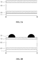
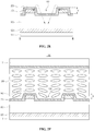
- FIGs. 2A to 2F are schematic cross-sectional views of an FFS mode LCD device in steps of manufacturing the same and correspond to a line II-II of FIG. 1 .
- the common electrode 60 is formed on a first substrate 11, and a passivation layer 80 is formed on the common electrode 60.
- a pixel electrode layer 72 is formed on the passivation layer 80.
- the common electrode 60 and the pixel electrode layer 72 are formed by depositing a transparent conductive material, for example, indium tin oxide (ITO).
- ITO indium tin oxide
- photoresist patterns 30 are formed on the pixel electrode layer 72 through a photolithographic process.
- the photoresist patterns 30 selectively expose the pixel electrode layer 72.
- FIG. 2C the exposed portions of the pixel electrode layer 72 of FIG. 2B are removed by wet-etching.
- FIG. 2D the pixel electrode 70 having openings OP is formed, and the photoresist pattern 30 of FIG. 2C is removed.
- an alignment layer 90 is formed on the pixel electrode 70.
- a second substrate 12 is attached to the first substrate 11 with liquid crystal molecules 98 between the first and second substrates 11 and 12 to thereby complete the FFS mode LCD device 100.
- the alignment layer 90 has a step height d due to the openings op of the pixel electrode 70.
- the passivation layer 80 under the pixel electrode 70 is partially removed during the wet etching step, and the passivation layer 80 has a first step height d1 of FIG. 2D .
- the pixel electrode 70 has a second step height d2 of FIG. 2D due to the openings op.
- the step height d of the alignment layer 90 is increased by the sum of the first and second step heights d1 and d2 of FIG. 2D .
- the step height d of the alignment layer 90 between an area where the pixel electrode 70 is formed and an area where the pixel electrode 70 is not formed causes a problem when the liquid crystal molecules 98 are driven.
- the liquid crystal molecules 90 are arranged in a rubbing direction of the alignment layer 90.
- the alignment layer 90 is not perfectly rubbed due to the step height d, and some of the liquid crystal molecules 98 are not regularly arranged in the rubbing direction and distorted. In addition, the liquid crystal molecules 98 adjacent to the second substrate 12 are also irregularly arranged over the step height d.
- phase retardation of light is caused due to the liquid crystal molecules 98 irregularly arranged around and over the step height d of the alignment layer 90.
- Linearly polarized light is changed into elliptically polarized light by the phase retardation, and the elliptically polarized light is outputted through a polarizer on the second substrate 12.
- one aspect of the present disclosure is to provide an LCD device that substantially obviates one or more of the problems due to limitations and disadvantages of the related art.
- An object of the present disclosure is to provide an LCD device that effectively improves light leakage and afterimage and a method for manufacturing the same.
- the main idea to solve this object is to provide a liquid crystal display device comprising: a first substrate; a thin film transistor on the first substrate; a passivation layer on the thin film transistor; a electrode of an oxide semiconductor on the passivation layer; and an alignment layer on the electrode, wherein the electrode includes first portions and second portions, wherein the second portions have a conductor property.
- a surface of the electrode facing the alignment layer is flat or formed planar.
- a liquid crystal display device including a first substrate; a thin film transistor on the first substrate; a first passivation layer on the thin film transistor; a first electrode on the first passivation layer; a second passivation layer on the first electrode; a second electrode of an oxide semiconductor on the second passivation layer; and an alignment layer on the second electrode, wherein the second electrode includes first portions and second portions, and the second portions have a conductor property. A surface of the second portions of the second electrode is flush with a surface of the first portions of the second electrode.
- the second electrode is formed of indium gallium zinc oxide (IG-ZO) and has a plate shape.
- IG-ZO indium gallium zinc oxide
- the first portions are bar-shaped and spaced apart from each other.
- the first electrode is formed of indium tin oxide (ITO) and has a plate shape.
- ITO indium tin oxide
- the first electrode is formed of indium tin oxide (ITO) and includes bar-shaped patterns.
- ITO indium tin oxide
- openings between the bar-shaped patterns correspond to the second portions.
- a liquid crystal display device in another aspect, includes a first substrate; a thin film transistor on the first substrate; a passivation layer on the thin film transistor; an electrode layer of an oxide semiconductor on the passivation layer; and an alignment layer on the electrode layer, wherein the electrode layer includes first portions, second portions and third portions, the first and second portions alternate each other, and each third portion is disposed between adjacent first and second portions, and wherein the first and second portions have a conductor property.
- the electrode layer is formed of indium gallium zinc oxide (IGZO) and has a plate shape.
- IGZO indium gallium zinc oxide
- the first, second and third portions are bar-shaped.
- a liquid crystal display device in another aspect, includes a first substrate and a second substrate facing each other; a thin film transistor on an inner surface of the first substrate; a passivation layer on the thin film transistor; a first electrode of an oxide semiconductor on the passivation layer; a first alignment layer on the first electrode; a second electrode of an oxide semiconductor on an inner surface of the second substrate; a second alignment layer on the second electrode; and a liquid crystal layer between the first and second alignment layers, wherein each of the first and second electrodes includes first portions and second portions, and the second portions of the first and second electrodes have a conductor property. A surface of the second portions of the first and second electrodes is flush with a surface of the first portions of the first and second electrodes.
- the first and second electrodes are formed of indium gallium zinc oxide (IGZO) and have a plate shape.
- IGZO indium gallium zinc oxide
- the first portions of the first and second electrodes are bar-shaped and spaced apart from each other.
- the first portions of the first electrode correspond to the second portions of the second electrode
- the second portions of the first electrode correspond to the first portions of the second electrode
- the first portions of the first electrode correspond to the first portions of the second electrode
- the second portions of the first electrode correspond to the second portions of the second electrode
- a method for manufacturing a liquid crystal display device comprising the steps of: providing a first substrate; providing a thin film transistor on the first substrate; forming a passivation layer on the thin film transistor; forming an electrode of an oxide semiconductor on the passivation layer; and forming first portions and second portions of the electrode, wherein the second portions have a conductor property by plasma treatment; forming an alignment layer on the electrode, providing a liquid crystal layer on the alignment layer; providing a second substrate facing the first substrate.
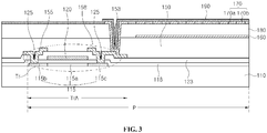
- FIG. 3 is a schematic cross-sectional view of an array substrate of an LCD device according to a first embodiment of the present invention.
- a semiconductor layer 115 is formed in a switching area TrA of each pixel region P on a first substrate 110.
- a gate insulating layer 118 is formed on the semiconductor layer 115 substantially all over the first substrate 110.
- a gate electrode 120 is formed on the gate insulating layer 118 corresponding to a central portion 115a of the semiconductor layer 115.
- the semiconductor layer 115 includes source and drain portions 115b and 115c at both sides of the central portion 115a. Impurities are highly doped in the source and drain portions 115b and 115c.
- An inter insulating layer 123 is formed on the gate electrode 120 substantially all over the first substrate 110.
- the inter insulating layer 123 includes semiconductor contact holes 125 exposing the source and drain portions 115b and 115c, respectively.
- Source and drain electrodes 155 and 158 are formed on the inter insulating layer 123.
- the source and drain electrodes 155 and 158 are spaced apart from each other and are connected to the source and drain portions 115b and 115c through the semiconductor contact holes 125, respectively.
- the semiconductor layer 115, the gate insulating layer 118, the gate electrode 120, the source electrode 155 and the drain electrode 158 in the switching area TrA constitute a thin film transistor Tr.
- the thin film transistor Tr is explained as a coplanar type, which may be also referred to as a top gate type and the type of the thin film transistor Tr is not limited to this.
- an inverted staggered type thin film transistor which may be also referred to as a bottom gate type, may be used.
- a first passivation layer 150 and a second passivation layer 180 may be formed on the source and drain electrodes 155 and 158.
- the first and second passivation layers 150 and 180 may have a drain contact hole 153 exposing the drain electrode 158.
- a first electrode 160 may be disposed between the first and second passivation layers 150 and 180.
- a second electrode 170 may be formed on the second passivation layer 180 and overlap the first electrode 160 in the pixel region P.
- the second electrode 170 contacts the drain electrode 158 through the drain contact hole 153.
- the first electrode 160 may contact the drain electrode 158 through the drain contact hole 153.
- the first electrode 160 may be separately formed in each pixel region P, and the second electrode 170 in the pixel region P may be connected to a second electrode in a next pixel region.
- a first alignment layer 190 is formed on the second electrode 170.
- the second passivation layer 180 is disposed between the first electrode 160 and the second electrode 170. When a voltage is applied, a fringe field is generated between the first electrode 160 and the second electrode 170.
- the LCD device including the array substrate according to the first embodiment may be a fringe field switching (FFS) mode.
- FFS fringe field switching
- one of the first electrode 160 and the second electrode 170 may be a pixel electrode, and the other may be a common electrode.
- the first electrode 160 may be a common electrode
- the second electrode 170 may be a pixel electrode.
- the LCD device further include a second substrate (not shown) spaced apart from and facing the first substrate 110.
- a black matrix (not shown) may be formed on an inner surface of the second substrate, and a color filter layer (not shown) including red, green and blue color filter patterns may be formed between patterns of the black matrix.
- an overcoat layer (not shown) may be formed on the color filter layer.
- the overcoat layer has a flat top surface and protects the color filter layer.
- a second alignment layer (not shown) is formed on the overcoat layer.
- the first substrate 110 and the second substrate are attached to each other with liquid crystal molecules (not shown) interposed therebetween to complete the FFS mode LCD device.
- the structure of the FFS mode LCD device is only one example and is not limited to this.
- the first electrode 160 and the second electrode 170 do not have specific patterns and have substantially a plate shape.
- the second electrode 170 does not have any pattern such as openings, and thus the first alignment layer 190 on the second electrode 170 does not have a step height d of FIG. 2E without an additional process.
- the light leakage and afterimage which are caused by the step height d of the alignment layer 90 due to the openings op of the second electrode 70 in FIG. 2E , can be effectively improved.
- FIGs. 4A to 4F are schematic cross-sectional views of the LCD device in steps of manufacturing the same according to the first embodiment of the present invention.
- the gate insulating layer 118, the inter insulating layer 123 and the first passivation layer 150 are sequentially formed on the first substrate 110.
- the first electrode 160 having a plate shape is formed on the first passivation layer 150, and the second passivation layer 180 is formed on the first electrode 160.
- a second electrode layer 172 is formed on the second passivation layer 180.
- the second electrode layer 172 may be separately patterned to correspond to each pixel region P of FIG. 3 .
- the first electrode 160 may be formed of a transparent conductive material.
- the first electrode 160 may be formed of indium tin oxide (ITO).
- the second passivation layer 180 on the first electrode 160 may be formed by depositing an inorganic insulating material such as silicon oxide (SiO2) or silicon nitride (SiNx), for example, or by applying an organic insulating material such as photo acryl, for example.
- an inorganic insulating material such as silicon oxide (SiO2) or silicon nitride (SiNx)
- an organic insulating material such as photo acryl, for example.
- the second electrode layer 172 may be formed of transparent indium gallium zinc oxide (IGZO).
- IGZO transparent indium gallium zinc oxide
- the IGZO is an oxide semiconductor.
- the IGZO may include a 1:1:1:3 mix of indium, gallium, zinc and oxygen, and the IGZO is not limited to this.
- the second electrode layer 172 may be formed on the second passivation layer 180 by depositing IGZO using a RF and DC magnetron sputtering method, a molecular beam epitaxy (MBE) method, a chemical vapor deposition (CVD) method, or a pulse laser deposition (PLD) method.
- a RF and DC magnetron sputtering method a molecular beam epitaxy (MBE) method, a chemical vapor deposition (CVD) method, or a pulse laser deposition (PLD) method.
- MBE molecular beam epitaxy
- CVD chemical vapor deposition
- PLD pulse laser deposition
- the sputtering method has advantages that a film can be easily formed, a thin film having a high quality can be deposited at a relatively low temperature, and it is easy to deposit a film for a relatively large size as compared with other methods.
- a photoresist layer is formed on the second electrode layer 172 and is patterned through a photolithographic process to thereby form photoresist patterns 130 on the second electrode layer 172.
- the photoresist patterns 130 selectively cover portions of the pixel electrode layer 172 and selectively expose the other portions of the pixel electrode layer 172.
- FIG. 4C plasma treatment is performed to the pixel electrode layer 172 of FIG. 4B such that the exposed portions of the pixel electrode layer 172 of FIG. 4B becomes a conductor, thereby forming the second electrode 170 including first portions 170a and second portions 170b.
- the second portions 170b of the second electrode 170 formed of IGZO oxygen vacancies are formed by ion impacts through the plasma treatment, and the oxygen vacancies function as dopants.
- the resistance of the second portions 170b of the second electrode 170 decreases, and the second portions 170b of the second electrode 170 have a conductor property.
- the oxygen vacancies are generated during the plasma treatment process, free electrons increase, and the conductivity of the second portions 170b of the second electrode 170 increases.
- argon (Ar), helium (He) or hydrogen (H2) may be used for the plasma treatment, and the gas for the plasma treatment is not limited to these.
- the first portions 170a and the second portions 170b may have a bar shape and may alternate each other. However, the first and second portions 170a and 170b are not limited to this.
- the photoresist patterns 130 cover one of the first portions 170a and the second portions 170b expose the other of the first portions 170a and the second portions 170b.
- the photoresist patterns 130 cover the first portions 170a and expose the second portions 170b.
- the photoresist patterns 130 may cover the second portions 170b and expose the first portions 170a.
- FIG. 4D the photoresist patterns 130 of FIG. 4C are removed through a stripping process.
- the first portions 170a of the second electrode 170 still have an oxide semiconductor property, and the second portions 170b of the second electrode 170 have a conductor property.
- the second portions 170b of the second electrode 170 and the first electrode 160 induce a fringe field therebetween such that liquid crystal molecules are driven by the fringe field.
- the second electrode 170 having a plate shape without any pattern.
- the first alignment layer 190 is formed on the second electrode 170.
- the second substrate 120 having the second alignment layer 191 is disposed over the first substrate 110 such that the second alignment layer 191 faces the first alignment layer 190.
- the liquid crystal molecules 198 are disposed between the first alignment layer 190 and the second alignment layer 191 to complete the LCD device 200.
- the first alignment layer 190 may be formed by forming a polymer thin film and orienting its surface in a predetermined direction.
- An organic material such as polyimide may be used for the first alignment layer 190, and the material for the first alignment layer 190 is not limited to this.
- a rubbing method or a UV irradiating method may be used to orient the surface of the first alignment layer 190.
- the rubbing method may be used. More specifically, an organic material of polyimide may be applied on a substrate, a solvent may be removed at a temperature of 60 to 80 °C, the organic material may be hardened at a temperature of 80 to 200 °C, thereby forming the first alignment layer 190, and the first alignment layer 190 may be rubbed by a rubbing cloth such as velvet in a predetermined direction.
- a rubbing cloth such as velvet in a predetermined direction.
- the rubbing method is easy and stable for orientation of an alignment layer and is appropriate for mass production.
- the first alignment layer 190 since the first alignment layer 190 is formed on the second electrode 170 having a flat surface, the first alignment layer 190 does not have a step height d of FIG. 2E . Thus, the surface of the first alignment layer 190 can be uniformly oriented, and the orientation problem of the first alignment layer 190 is prevented.
- liquid crystal molecules 198 between the first and second alignment layers 190 and 191 are regularly arranged in a predetermined direction.
- the surface of the second alignment layer 191 also may be oriented by the rubbing method or the UV irradiating method.
- the first electrode 160 is formed of ITO and has a plate shape.
- the second electrode 170 is formed of IGZO and has a plate shape, and the second portions 170b of the second electrode 170 are plasma-treated to have a conductor property.
- the fringe field is generated between the first electrode 160 and the second portions 170b of the second electrode 170 when a voltage is applied.
- the first alignment layer 190 on the second electrode 170 does not have a step height d of FIG. 2E , and the liquid crystal molecules 198 are regularly arranged in the predetermined direction. Accordingly, the afterimage of the LCD device 200 can be effectively improved.
- FIG. 5 is a schematic cross-sectional view of an LCD device according to a second embodiment of the present invention and show a pixel region.
- the LCD device according to the second embodiment of the present invention has substantially the same structure as the first embodiment excluding the first electrode. For convenience, detailed explanation will be omitted or shortened for the same or similar parts.
- the LCD device 300 includes a first electrode 260 having bar-shaped patterns and a second electrode 270 having a plate shape without any particular pattern.
- a first alignment layer 290 on the second electrode 270 does not have a step height d of FIG. 2E without an additional process.
- a first passivation layer 250 is formed on a first substrate 210, and the first electrode 260 is formed on the first passivation layer 250.
- the first electrode 260 includes bar-shaped patterns.
- a second passivation layer 280 is formed on the first electrode 260.
- the second electrode 270 having a plate shape is formed on the second passivation layer 280.
- the first electrode 260 may be formed of a transparent conductive material.
- the first electrode 260 may be formed of indium tin oxide (ITO) or indium zinc oxide (IZO).
- the first electrode 260 may be formed on the first passivation layer 250 by depositing a transparent conductive material such as ITO or IZO substantially all over the first passivation layer 250 to thereby form a transparent conductive layer and then patterning the transparent conductive layer.
- a transparent conductive material such as ITO or IZO substantially all over the first passivation layer 250 to thereby form a transparent conductive layer and then patterning the transparent conductive layer.
- the second passivation layer 280 on the first electrode 260 may be formed by depositing an inorganic insulating material such as silicon oxide (SiO2) or silicon nitride (SiNx), for example, or by applying an organic insulating material such as photo acryl, for example.
- an inorganic insulating material such as silicon oxide (SiO2) or silicon nitride (SiNx)
- an organic insulating material such as photo acryl, for example.
- the second electrode 270 may be formed of transparent indium gallium zinc oxide (IGZO).
- IGZO transparent indium gallium zinc oxide
- the IGZO is an oxide semiconductor.
- the IGZO may include a 1:1:1:3 mix of indium, gallium, zinc and oxygen, and the IGZO is not limited to this.
- the second electrode 270 may be formed on the second passivation layer 280 by depositing IGZO using a RF and DC magnetron sputtering method, a molecular beam epitaxy (MBE) method, a chemical vapor deposition (CVD) method, or a pulse laser deposition (PLD) method.
- a RF and DC magnetron sputtering method a molecular beam epitaxy (MBE) method, a chemical vapor deposition (CVD) method, or a pulse laser deposition (PLD) method.
- MBE molecular beam epitaxy
- CVD chemical vapor deposition
- PLD pulse laser deposition
- the sputtering method has advantages that a film can be easily formed, a thin film having a high quality can be deposited at a relatively low temperature, and it is easy to deposit a film for a relatively large size as compared with other methods.
- a photoresist layer may be formed on a layer for the second electrode 270 and may be patterned through a photolithographic process to thereby form photoresist patterns 130 of FIG. 4C on the layer for the second electrode 270.
- the photoresist patterns 130 of FIG. 4C may selectively cover portions of the layer for the second electrode 270 and selectively expose the other portions of the layer for the second electrode 270.
- plasma treatment may be performed to the layer for the second electrode 270 on which the photoresist patterns 130 of FIG. 4C such that the exposed portions of the layer of the second electrode 270 may become a conductor, thereby forming the second electrode 270 including first portions 270a and second portions 270b.
- oxygen vacancies may be formed by ion impacts through the plasma treatment, and the oxygen vacancies may function as dopants.
- the resistance of the second portions 270b of the second electrode 270 may decrease, and the second portions 270b of the second electrode 270 may have a conductor property.
- the oxygen vacancies may be generated during the plasma treatment process, free electrons may increase, and the conductivity of the second portions 270b of the second electrode 270 may increase.
- argon (Ar), helium (He) or hydrogen (H2) may be used for the plasma treatment, and the gas for the plasma treatment is not limited to these.
- the first portions 270a and the second portions 270b may have a bar shape and may alternate each other. However, the first and second portions 270a and 270b are not limited to this.
- the second portions 270b of the second electrode 270 may correspond to openings between the bar-shaped patterns of the first electrode 260.
- the first portions 270a of the second electrode 270 may correspond to the bar-shaped patterns of the first electrode 260.
- the photoresist patterns 130 of FIG. 4C may cover the first portions 270a and expose the second portions 270b.
- the photoresist patterns 130 of FIG. 4C may be removed through a stripping process.
- the first portions 270a of the second electrode 270 still may have an oxide semiconductor property
- the second portions 270b of the second electrode 270 may have a conductor property.
- the second portions 270b of the second electrode 270 may correspond to or may be arranged opposite to or facing the openings between the bar-shaped patterns of the first electrode 260, and the second portions 270b of the second electrode 270 and the first electrode 260 may induce a horizontal electric field therebetween such that liquid crystal molecules 298 are driven by the horizontal electric field, which is substantially parallel to the first and second substrate 210 and 220.
- first electrode 260 having the bar-shaped patterns with the openings therebetween and the second electrode having a plate shape without any pattern.
- the second electrode 270 having a plate shape without any pattern can be formed.
- the first alignment layer 290 is formed on the second electrode 270.
- the first alignment layer 290 may be formed by forming a polymer thin film and orienting its surface in a predetermined direction.
- An organic material such as polyimide may be used for the first alignment layer 290, and the material for the first alignment layer 290 is not limited to this.
- a rubbing method may be used to orient the surface of the first alignment layer 290.
- an organic material of polyimide may be applied on a substrate, a solvent may be removed at a temperature of 60 to 80 °C, the organic material may be hardened at a temperature of 80 to 200 °C, thereby forming the first alignment layer 290, and the first alignment layer 290 may be rubbed by a rubbing cloth such as velvet in a predetermined direction.
- the rubbing method is easy and stable for orientation of an alignment layer and is appropriate for mass production.
- the first alignment layer 290 since the first alignment layer 290 is formed on the second electrode 270 having a flat surface, the first alignment layer 290 does not have a step height d of FIG. 2E . Thus, the surface of the first alignment layer 290 can be uniformly oriented, and the orientation problem of the first alignment layer 290 may be prevented.
- first substrate 210 and a second substrate 220 facing the first substrate 210 are attached to each other with liquid crystal molecules 298 interposed therebetween to thereby complete an IPS mode LCD device 300.
- liquid crystal molecules 298 between the first alignment layer 290 and a second alignment layer 291 are regularly arranged in a predetermined direction.
- the first electrode 260 has bar-shaped patterns.
- the second electrode 270 is formed of IGZO and has a plate shape.
- the second portions 270b of the second electrode 270 are plasma-treated to have a conductor property.
- the bar-shaped patterns of the first electrode 260 and the second portions 270b of the second electrode 270 are alternately arranged to generate a horizontal electric field which is parallel to the first and second substrates 210 and 220 when a voltage is applied.
- the liquid crystal molecules 298 are driven by the horizontal electric field.
- the first alignment layer 290 on the second electrode 270 does not have a step height d of FIG. 2E , and the liquid crystal molecules 298 are regularly arranged in the predetermined direction. Accordingly, the light leakage and afterimage of the LCD device 300 can be effectively improved.
- FIG. 6 is a schematic cross-sectional view of an LCD device according to a third embodiment of the present invention and show a pixel region.
- the LCD device according to the third embodiment of the present invention has substantially the same structure as the first embodiment excluding the first electrode and the second electrode. For convenience, detailed explanation will be omitted or shortened for the same or similar parts.
- the LCD device 400 includes a single electrode layer 370 having a plate shape and including a first electrode 370a and a second electrode 370b.
- the single electrode layer 370 includes first portions 370a of the first electrode and second portions 370b of the second electrode which alternate each other, a first alignment layer 390 on the single electrode layer 370 does not have a step height d of FIG. 2E without an additional process.
- a passivation layer 350 is formed on a first substrate 310, and the single electrode layer 370 having a plate shape is formed on the passivation layer 350.
- the passivation layer 350 may be formed by depositing an inorganic insulating material such as silicon oxide (SiO2) or silicon nitride (SiNx), for example, or by applying an organic insulating material such as photo acryl, for example.
- an inorganic insulating material such as silicon oxide (SiO2) or silicon nitride (SiNx)
- an organic insulating material such as photo acryl
- the single electrode layer 370 on the passivation layer 350 may be formed of transparent indium gallium zinc oxide (IGZO).
- IGZO transparent indium gallium zinc oxide
- the IGZO is an oxide semiconductor.
- the IGZO may include a 1:1:1:3 mix of indium, gallium, zinc and oxygen, and the IGZO is not limited to this.
- the single electrode layer 370 may be formed on the passivation layer 350 by depositing IGZO using a RF and DC magnetron sputtering method, a molecular beam epitaxy (MBE) method, a chemical vapor deposition (CVD) method, or a pulse laser deposition (PLD) method.
- a RF and DC magnetron sputtering method a molecular beam epitaxy (MBE) method
- MBE molecular beam epitaxy
- CVD chemical vapor deposition
- PLD pulse laser deposition
- the sputtering method has advantages that a film can be easily formed, a thin film having a high quality can be deposited at a relatively low temperature, and it is easy to deposit a film for a relatively large size as compared with other methods.
- a photoresist layer may be formed on the single electrode layer 370 and may be patterned through a photolithographic process to thereby form photoresist patterns 130 of FIG. 4C on the single electrode layer 370.
- the photoresist patterns 130 of FIG. 4C may selectively cover portions of the single electrode layer 370 and selectively expose the other portions of the single electrode layer 370.
- plasma treatment may be performed to the single electrode layer 370 on which the photoresist patterns 130 of FIG. 4C such that the exposed portions of the single electrode layer 370 may become a conductor, thereby forming the first portions 370a and the second portions 370b.
- oxygen vacancies may be formed by ion impacts through the plasma treatment, and the oxygen vacancies may function as dopants.
- the resistance of the first and second portions 370a and 370b of the single electrode layer 370 may decrease, and the first and second portions 370a and 370b of the single electrode layer 370 may have a conductor property.
- the oxygen vacancies may be generated during the plasma treatment process, free electrons may increase, and the conductivity of the first and second portions 370a and 370b of the single electrode layer 370 may increase.
- argon (Ar), helium (He) or hydrogen (H2) may be used for the plasma treatment, and the gas for the plasma treatment is not limited to these.
- the single electrode layer 370 includes first, second and third portions 370a, 370b and 370c.
- the first portions 370a and the second portions 370b may have a bar shape and may alternate each other.
- Each of the third portions 370c is disposed between adjacent first and second portions 370a and 370b.
- the first, second and third portions 370a, 370b and 370c are not limited to this.
- first portion 370a, the third portion 370c, the second portion 370b, the third portion 370c, the first portion 370a, the third portion 370c, and so on may be sequentially arranged, and the order is not limited on this.
- first and second portions 370a and 370b of the single electrode layer 370 may have a conductor property and the third portions 370c of the single electrode layer 370 may have an oxide semiconductor property.
- the photoresist patterns 130 of FIG. 4C may cover the third portions 370c of the single electrode layer 370 and expose the first and second portions 370a and 370b of the single electrode layer 370.
- the photoresist patterns 130 of FIG. 4C may be removed through a stripping process.
- the third portions 370c of the single electrode layer 370 still may have an oxide semiconductor property, and the first and second portions 370a and 370b of the single electrode 370 may have a conductor property.
- the first and second portions 370a and 370b of the single electrode layer 370 may function as the first and second electrodes, respectively.
- one of the first and second portions 370a and 370b may be a pixel electrode which is connected to a thin film transistor, and the other one of the first and second portions 370a and 370b may be a common electrode which is connected to a common line.
- the first electrode corresponding to the first portions 370a of the single electrode layer 370 and the second electrode corresponding to the second portions 370b of the single electrode layer 370b may induce a horizontal electric field therebetween such that liquid crystal molecules 398 are driven by the horizontal electric field, which is substantially parallel to the first and second substrate 310 and 320.
- the first alignment layer 390 is formed on the single electrode layer 370 having a plate shape and including the first and second electrodes 370a and 370b.
- the first substrate 310 having the single electrode layer 370 and a second substrate 320 facing the first substrate 310 are attached to each other with liquid crystal molecules 398 interposed therebetween to thereby complete an IPS mode LCD device 400.
- the single electrode layer 370 is formed of IGZO and has a plate shape, and the first and second portions 370a and 370b, which function as the first and second electrodes, are plasma-treated to have a conductor property.
- the first and second portions 370a and 370b are alternately arranged with the third portions 370c therebetween to generate a horizontal electric field which is parallel to the first and second substrates 310 and 320 when a voltage is applied.
- the liquid crystal molecules 298 may be driven by the electric field.
- the first alignment layer 390 on the single electrode layer 370 does not have a step height d of FIG. 2E , and the liquid crystal molecules 398 are regularly arranged in the predetermined direction. Accordingly, the light leakage and afterimage of the LCD device 400 can be effectively improved.
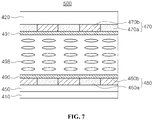
- FIG. 7 is a schematic cross-sectional view of an LCD device according to a fourth embodiment of the present invention and show a pixel region.
- the LCD device according to the fourth embodiment of the present invention has substantially the same structure as the first embodiment excluding the first electrode and the second electrode. For convenience, detailed explanation will be omitted or shortened for the same or similar parts.
- the LCD device 500 includes a first substrate 410, a second substrate 420 facing the first substrate 410, a first electrode 460 on an inner surface of he first substrate 410, a second electrode 470 on an inner surface of the second substrate 420, and liquid crystal molecules 498 between the first electrode 460 and the second electrode 470.
- a passivation layer 450 is formed between the first electrode 460 and the first substrate 410.
- the first electrode 460 and the second electrode 470 each have a plate shape without any particular pattern.
- each of a first alignment layer 490 on the first electrode 460 and a second alignment layer 491 on the second electrode 470 does not have a step height d of FIG. 2E without an additional process.
- first and second electrodes 460 and 470 may be formed of transparent indium gallium zinc oxide (IGZO).
- IGZO transparent indium gallium zinc oxide
- the IGZO is an oxide semiconductor.
- the IGZO may include a 1:1:1:3 mix of indium, gallium, zinc and oxygen, and the IGZO is not limited to this.
- each of the first and second electrodes 460 and 470 may include first portions 460a and 470a and second portions 460b and 470b.
- the first portions 460a of the first electrode 460 may correspond to the second portions 470b of the second electrode 470
- the second portions 460b of the first electrode 460 may correspond to the first portions 470a of the second electrode 470.
- first portions 460a of the first electrode 460 may correspond to the first portions 470a of the second electrode 470
- the second portions 460b of the first electrode 460 may correspond to the second portions 470b of the second electrode 470.
- first portions 460a and 470a and the second portions 460b and 470b may be alternately arranged, and are not limited to this.
- photoresist patterns 130 of FIG. 4C may be formed on each of the first and second electrodes 460 and 470, and the photoresist patterns 130 of FIG. 4C may selectively cover ones of the first portions 460a and 470a and the second portions 460b and 470b of the first and second electrodes 460 and 470 and selectively expose the others.
- the photoresist patterns 130 of FIG. 4C may selectively cover the first portions 460a and 470a of the first and second electrodes 460 and 470 and selectively expose the second portions 460b and 470b of the first and second electrodes 460 and 470.
- plasma treatment may be performed to the first and second electrodes 460 and 470 on which the photoresist patterns 130 of FIG. 4C such that the exposed second portions 460b and 470b of the first and second electrodes 460 and 470 may become a conductor.
- oxygen vacancies may be formed by ion impacts through the plasma treatment, and the oxygen vacancies may function as dopants.
- the resistance of the second portions 460b and 470b of the first and second electrodes 460 and 470 may decrease, and the second portions 460b and 470b of the first and second electrodes 460 and 470 may have a conductor property.
- the oxygen vacancies may be generated during the plasma treatment process, free electrons may increase, and the conductivity of the second portions 460b and 470b of the first and second electrodes 460 and 470 may increase.
- argon (Ar), helium (He) or hydrogen (H2) may be used for the plasma treatment, and the gas for the plasma treatment is not limited to these.
- the photoresist patterns 130 of FIG. 4C may be removed through a stripping process.
- the first portions 460a and 470a of the first and second electrodes 460 and 470 still may have an oxide semiconductor property
- the second portions 460b and 470b of the first and second electrodes 460 and 470 may have a conductor property.
- the second portions 460b of the first electrode 460 and the second portions 470b of the second electrode 470 may induce a vertical electric field therebetween such that liquid crystal molecules 498 are driven by the vertical electric field, which is substantially perpendicular to the first and second substrates 410 and 420.
- the first and second electrodes 460 and 470 each have a plate shape without patterns.
- the first and second alignment layers 490 and 491 are formed on the first and second electrodes 460 and 470, respectively.
- first and second electrodes 460 and 470 have flat surfaces, the first and the second alignment layers 490 and 491 do not have a step height d of FIG. 2E . Thus, surfaces of the first and second electrodes 460 and 470 are uniformly oriented.
- liquid crystal molecules 498 on the first and second alignment layers 490 and 491 are regularly arranged in the predetermined direction.
- the first and second electrodes 460 and 470 are formed of IGZO and have a plate shape.
- the second portions 460 and 470b of the first and second electrodes 460 and 470 are plasma-treated to have a conductor property.
- the second portions 460 and 470b of the first and second electrodes 460 and 470 are alternated arranged to generate a vertical electric field which is perpendicular to the first and second substrates 410 and 420 when a voltage is applied.
- the liquid crystal molecules 498 are regularly arranged in the predetermined direction. Accordingly, the light leakage and afterimage of the LCD device 500 can be effectively improved.
- the electrode is formed to partially be a conductor, and the alignment layer is formed on the electrode without a step height.
- the LCD device improving the afterimage can be provided without an increase in manufacturing processes as compared with the related art.
Landscapes
- Physics & Mathematics (AREA)
- Nonlinear Science (AREA)
- Mathematical Physics (AREA)
- Chemical & Material Sciences (AREA)
- Crystallography & Structural Chemistry (AREA)
- General Physics & Mathematics (AREA)
- Optics & Photonics (AREA)
- Engineering & Computer Science (AREA)
- Microelectronics & Electronic Packaging (AREA)
- Geometry (AREA)
- Spectroscopy & Molecular Physics (AREA)
- Liquid Crystal (AREA)
Abstract
Description
- The present application claims priority from and the benefit of Korean Patent Application No.
10-2016-0143759 - The present disclosure relates to a liquid crystal display device, and more particularly, to a liquid crystal display device capable of effectively improving light leakage and afterimage and to a method for manufacturing the same.
- In general, liquid crystal display (LCD) devices are driven based on optical anisotropy and polarization characteristics of liquid crystal. Liquid crystal molecules have a long and thin shape, and the liquid crystal molecules are regularly arranged along in an alignment direction. The alignment of the liquid crystal molecules depends on the intensity or the direction of an electric field applied to the liquid crystal molecules.
- By controlling the alignment of the liquid crystal molecules, light is refracted along the alignment of the liquid crystal molecules, thereby displaying images.
- Since the LCD device including thin film transistors as a switching element, referred to as an active matrix LCD (AM-LCD) device, has excellent characteristics of high resolution and displaying moving images, the AM-LCD device has been widely used.
- The LCD device includes two substrates, which are spaced apart and facing each other, and a liquid crystal layer is interposed between the two substrates. Each of the substrates includes an electrode. The electrodes from respective substrates face one another. A vertical electric field is induced between the electrodes in a direction perpendicular to the substrates by applying a voltage to each electrode. The LCD device driven by the vertical electric field has relatively high transmittance and aperture ratio.
- In addition, an in-plane switching (IPS) mode LCD device, in which electrodes are formed on one substrate, has been suggested and developed.
- Generally, the IPS mode LCD device includes an array substrate including thin film transistors, a color filter substrate including color filters, and a liquid crystal layer between the array substrate and the color filter substrate. The IPS mode LCD device controls light transmittance of the liquid crystal layer with a dielectric anisotropy using an electric field to display images.
- The array substrate includes the thin film transistor, a pixel electrode and a common electrode in each of pixel regions defined by crossing of gate lines and data lines. The thin film transistor supplies a data signal from the data line to the pixel electrode according to a gate signal from the gate line. The pixel electrode receives the data signal through the thin film transistor and drives liquid crystal molecules, and the common electrode receives a common voltage as a base for driving the liquid crystal molecules. The liquid crystal molecules rotate according to an electric field induced by the data signal of the pixel electrode and the common voltage of the common electrode and control the light transmittance to thereby achieve gray scales.
- Recently, a fringe field switching (FFS) mode LCD device has been suggested to provide better viewing angle properties.
-
FIG. 1 is a schematic view of an FFS mode LCD device according to the related art. - In
FIG. 1 , the FFSmode LCD device 100 includes agate line 43 in a direction and adata line 51 crossing thegate line 43 to define a pixel region P. - A thin film transistor Tr is disposed in the pixel region P and is connected to the
gate line 43 and thedata line 51. The thin film transistor Tr includes agate electrode 45, a gate insulating layer (not shown), a semiconductor layer (not shown), asource electrode 55 and adrain electrode 58. - In addition, a
common electrode 60 having a plate shape in the pixel region P is formed substantially all over a display area including the pixel region P. Here, thecommon electrode 60 is shown by a dotted line corresponding to the pixel region P. - Moreover, a
pixel electrode 70 having a plurality of openings op is formed in the pixel region P. Thepixel electrode 70 overlaps thecommon electrode 60. Each opening op has a bar shape. - In the FFS mode LCD device, voltages are applied to the
common electrode 60 and thepixel electrode 70 in the pixel region P to induce a fringe field therebetween. -
FIGs. 2A to 2F are schematic cross-sectional views of an FFS mode LCD device in steps of manufacturing the same and correspond to a line II-II ofFIG. 1 . - In
FIG. 2A , thecommon electrode 60 is formed on afirst substrate 11, and apassivation layer 80 is formed on thecommon electrode 60. Apixel electrode layer 72 is formed on thepassivation layer 80. - Here, the
common electrode 60 and thepixel electrode layer 72 are formed by depositing a transparent conductive material, for example, indium tin oxide (ITO). - In
FIG. 2B ,photoresist patterns 30 are formed on thepixel electrode layer 72 through a photolithographic process. Thephotoresist patterns 30 selectively expose thepixel electrode layer 72. - In
FIG. 2C , the exposed portions of thepixel electrode layer 72 ofFIG. 2B are removed by wet-etching. - In
FIG. 2D , thepixel electrode 70 having openings OP is formed, and thephotoresist pattern 30 ofFIG. 2C is removed. - In
FIG. 2E , analignment layer 90 is formed on thepixel electrode 70. - In
FIG. 2F , asecond substrate 12 is attached to thefirst substrate 11 withliquid crystal molecules 98 between the first andsecond substrates mode LCD device 100. - Here, the
alignment layer 90 has a step height d due to the openings op of thepixel electrode 70. - Moreover, the
passivation layer 80 under thepixel electrode 70 is partially removed during the wet etching step, and thepassivation layer 80 has a first step height d1 ofFIG. 2D . Thepixel electrode 70 has a second step height d2 ofFIG. 2D due to the openings op. Thus, the step height d of thealignment layer 90 is increased by the sum of the first and second step heights d1 and d2 ofFIG. 2D . - The step height d of the
alignment layer 90 between an area where thepixel electrode 70 is formed and an area where thepixel electrode 70 is not formed causes a problem when theliquid crystal molecules 98 are driven. - First, in a normally black mode, a voltage is not applied to the
liquid crystal molecules 98, and black is displayed. - Namely, when a voltage is not applied, the
liquid crystal molecules 90 are arranged in a rubbing direction of thealignment layer 90. - However, the
alignment layer 90 is not perfectly rubbed due to the step height d, and some of theliquid crystal molecules 98 are not regularly arranged in the rubbing direction and distorted. In addition, theliquid crystal molecules 98 adjacent to thesecond substrate 12 are also irregularly arranged over the step height d. - Therefore, phase retardation of light is caused due to the
liquid crystal molecules 98 irregularly arranged around and over the step height d of thealignment layer 90. Linearly polarized light is changed into elliptically polarized light by the phase retardation, and the elliptically polarized light is outputted through a polarizer on thesecond substrate 12. - As a result, in the normally black mode, when a voltage is not applied, there is a problem of light leakage.
- Moreover, there is another problem of an afterimage that a previous image overlaps a new image because of poor response of the
liquid crystal molecules 98 irregularly arranged around the step height d of thealignment layer 90. - Theses problems are caused in an IPS mode LCD device and a vertical alignment (VA) mode LCD device in addition to the FFS mode LCD device.
- Accordingly, one aspect of the present disclosure is to provide an LCD device that substantially obviates one or more of the problems due to limitations and disadvantages of the related art.
- An object of the present disclosure is to provide an LCD device that effectively improves light leakage and afterimage and a method for manufacturing the same.
- Additional features and advantages of the invention will be set forth in the description which follows, and in part will be apparent from the description, or may be learned by practice of the invention. The objectives and other advantages of the invention will be realized and attained by the structure particularly pointed out in the written description and claims hereof as well as the appended drawings.
- The objects are solved by the features of the independent claims. Preferred embodiments are given by the dependent claims.
- The main idea to solve this object is to provide a liquid crystal display device comprising: a first substrate; a thin film transistor on the first substrate; a passivation layer on the thin film transistor; a electrode of an oxide semiconductor on the passivation layer; and an alignment layer on the electrode, wherein the electrode includes first portions and second portions, wherein the second portions have a conductor property.
- Preferably, a surface of the electrode facing the alignment layer is flat or formed planar.
- To achieve these and other advantages and in accordance with the purpose of the present invention, as embodied and broadly described herein, there is provided a liquid crystal display device including a first substrate; a thin film transistor on the first substrate; a first passivation layer on the thin film transistor; a first electrode on the first passivation layer; a second passivation layer on the first electrode; a second electrode of an oxide semiconductor on the second passivation layer; and an alignment layer on the second electrode, wherein the second electrode includes first portions and second portions, and the second portions have a conductor property. A surface of the second portions of the second electrode is flush with a surface of the first portions of the second electrode.
- Preferably, wherein the second electrode is formed of indium gallium zinc oxide (IG-ZO) and has a plate shape.
- Preferably, the first portions are bar-shaped and spaced apart from each other.
- Preferably, the first electrode is formed of indium tin oxide (ITO) and has a plate shape.
- Preferably, the first electrode is formed of indium tin oxide (ITO) and includes bar-shaped patterns.
- Preferably, openings between the bar-shaped patterns correspond to the second portions.
- In another aspect, a liquid crystal display device includes a first substrate; a thin film transistor on the first substrate; a passivation layer on the thin film transistor; an electrode layer of an oxide semiconductor on the passivation layer; and an alignment layer on the electrode layer, wherein the electrode layer includes first portions, second portions and third portions, the first and second portions alternate each other, and each third portion is disposed between adjacent first and second portions, and wherein the first and second portions have a conductor property.
- Preferably, the electrode layer is formed of indium gallium zinc oxide (IGZO) and has a plate shape.
- Preferably, the first, second and third portions are bar-shaped.
- In another aspect, a liquid crystal display device includes a first substrate and a second substrate facing each other; a thin film transistor on an inner surface of the first substrate; a passivation layer on the thin film transistor; a first electrode of an oxide semiconductor on the passivation layer; a first alignment layer on the first electrode; a second electrode of an oxide semiconductor on an inner surface of the second substrate; a second alignment layer on the second electrode; and a liquid crystal layer between the first and second alignment layers, wherein each of the first and second electrodes includes first portions and second portions, and the second portions of the first and second electrodes have a conductor property. A surface of the second portions of the first and second electrodes is flush with a surface of the first portions of the first and second electrodes.
- Preferably, the first and second electrodes are formed of indium gallium zinc oxide (IGZO) and have a plate shape.
- Preferably, the first portions of the first and second electrodes are bar-shaped and spaced apart from each other.
- Preferably, the first portions of the first electrode correspond to the second portions of the second electrode, and the second portions of the first electrode correspond to the first portions of the second electrode.
- Preferably, the first portions of the first electrode correspond to the first portions of the second electrode, and the second portions of the first electrode correspond to the second portions of the second electrode.
- The object is also solved by a method for manufacturing a liquid crystal display device, comprising the steps of: providing a first substrate; providing a thin film transistor on the first substrate; forming a passivation layer on the thin film transistor; forming an electrode of an oxide semiconductor on the passivation layer; and forming first portions and second portions of the electrode, wherein the second portions have a conductor property by plasma treatment; forming an alignment layer on the electrode, providing a liquid crystal layer on the alignment layer; providing a second substrate facing the first substrate.
- Further scope of applicability of the present invention will become apparent from the detailed description given hereinafter. However, the detailed description and specific examples, while indicating preferred embodiments of the invention, are given by illustration only, since various changes and modifications within the scope of the invention will become apparent to those skilled in the art from this detailed description.
- The accompanying drawings, which are included to provide a further understanding of the invention and are incorporated in and constitute a part of this specification, illustrate embodiments of the invention and together with the description serve to explain the principles of the invention. In the drawings:
-
FIG. 1 is a schematic view of an FFS mode LCD device according to the related art; -
FIGs. 2A to 2F are schematic cross-sectional views of an FFS mode LCD device in steps of manufacturing the same and correspond to a line II-II ofFIG. 1 ; -
FIG. 3 is a schematic cross-sectional view of an array substrate of an LCD device according to a first embodiment of the present invention; -
FIGs. 4A to 4F are schematic cross-sectional views of the LCD device in steps of manufacturing the same according to the first embodiment of the present invention; -
FIG. 5 is a schematic cross-sectional view of an LCD device according to a second embodiment of the present invention; -
FIG. 6 is a schematic cross-sectional view of an LCD device according to a third embodiment of the present invention; and -
FIG. 7 is a schematic cross-sectional view of an LCD device according to a fourth embodiment of the present invention. - Reference will now be made in detail to the embodiment of the disclosure, an example of which is illustrated in the accompanying drawings. Words of 'on' and 'under' are used only for describing a direction in the following explanations and thus are not limited to 'directly on' and 'directly under'.
-
FIG. 3 is a schematic cross-sectional view of an array substrate of an LCD device according to a first embodiment of the present invention. - In
FIG. 3 , asemiconductor layer 115 is formed in a switching area TrA of each pixel region P on afirst substrate 110. Agate insulating layer 118 is formed on thesemiconductor layer 115 substantially all over thefirst substrate 110. Agate electrode 120 is formed on thegate insulating layer 118 corresponding to acentral portion 115a of thesemiconductor layer 115. Thesemiconductor layer 115 includes source and drainportions central portion 115a. Impurities are highly doped in the source and drainportions - An
inter insulating layer 123 is formed on thegate electrode 120 substantially all over thefirst substrate 110. Theinter insulating layer 123 includes semiconductor contact holes 125 exposing the source and drainportions - Source and
drain electrodes inter insulating layer 123. The source and drainelectrodes portions - The
semiconductor layer 115, thegate insulating layer 118, thegate electrode 120, thesource electrode 155 and thedrain electrode 158 in the switching area TrA constitute a thin film transistor Tr. - Here, the thin film transistor Tr is explained as a coplanar type, which may be also referred to as a top gate type and the type of the thin film transistor Tr is not limited to this. Alternatively, an inverted staggered type thin film transistor, which may be also referred to as a bottom gate type, may be used.
- A
first passivation layer 150 and asecond passivation layer 180 may be formed on the source and drainelectrodes drain contact hole 153 exposing thedrain electrode 158. Afirst electrode 160 may be disposed between the first and second passivation layers 150 and 180. Asecond electrode 170 may be formed on thesecond passivation layer 180 and overlap thefirst electrode 160 in the pixel region P. - In the first embodiment, the
second electrode 170 contacts thedrain electrode 158 through thedrain contact hole 153. Alternatively, thefirst electrode 160 may contact thedrain electrode 158 through thedrain contact hole 153. In this case, thefirst electrode 160 may be separately formed in each pixel region P, and thesecond electrode 170 in the pixel region P may be connected to a second electrode in a next pixel region. - A
first alignment layer 190 is formed on thesecond electrode 170. - The
second passivation layer 180 is disposed between thefirst electrode 160 and thesecond electrode 170. When a voltage is applied, a fringe field is generated between thefirst electrode 160 and thesecond electrode 170. - Like this, the LCD device including the array substrate according to the first embodiment may be a fringe field switching (FFS) mode.
- Here, one of the
first electrode 160 and thesecond electrode 170 may be a pixel electrode, and the other may be a common electrode. For example, thefirst electrode 160 may be a common electrode, and thesecond electrode 170 may be a pixel electrode. - The LCD device according to the first embodiment further include a second substrate (not shown) spaced apart from and facing the
first substrate 110. A black matrix (not shown) may be formed on an inner surface of the second substrate, and a color filter layer (not shown) including red, green and blue color filter patterns may be formed between patterns of the black matrix. - In addition, an overcoat layer (not shown) may be formed on the color filter layer. The overcoat layer has a flat top surface and protects the color filter layer. A second alignment layer (not shown) is formed on the overcoat layer.
- The
first substrate 110 and the second substrate are attached to each other with liquid crystal molecules (not shown) interposed therebetween to complete the FFS mode LCD device. - The structure of the FFS mode LCD device is only one example and is not limited to this.
- In the FFS mode LCD device according to the first embodiment of the present invention, the
first electrode 160 and thesecond electrode 170 do not have specific patterns and have substantially a plate shape. - Namely, the
second electrode 170 does not have any pattern such as openings, and thus thefirst alignment layer 190 on thesecond electrode 170 does not have a step height d ofFIG. 2E without an additional process. - Therefore, the light leakage and afterimage, which are caused by the step height d of the
alignment layer 90 due to the openings op of thesecond electrode 70 inFIG. 2E , can be effectively improved. -
FIGs. 4A to 4F are schematic cross-sectional views of the LCD device in steps of manufacturing the same according to the first embodiment of the present invention. - In
FIG. 4A , thegate insulating layer 118, theinter insulating layer 123 and thefirst passivation layer 150 are sequentially formed on thefirst substrate 110. Thefirst electrode 160 having a plate shape is formed on thefirst passivation layer 150, and thesecond passivation layer 180 is formed on thefirst electrode 160. Asecond electrode layer 172 is formed on thesecond passivation layer 180. Thesecond electrode layer 172 may be separately patterned to correspond to each pixel region P ofFIG. 3 . - Here, the
first electrode 160 may be formed of a transparent conductive material. For example, thefirst electrode 160 may be formed of indium tin oxide (ITO). - In addition, the
second passivation layer 180 on thefirst electrode 160 may be formed by depositing an inorganic insulating material such as silicon oxide (SiO2) or silicon nitride (SiNx), for example, or by applying an organic insulating material such as photo acryl, for example. - Meanwhile, the
second electrode layer 172 may be formed of transparent indium gallium zinc oxide (IGZO). - The IGZO is an oxide semiconductor. The IGZO may include a 1:1:1:3 mix of indium, gallium, zinc and oxygen, and the IGZO is not limited to this.
- The
second electrode layer 172 may be formed on thesecond passivation layer 180 by depositing IGZO using a RF and DC magnetron sputtering method, a molecular beam epitaxy (MBE) method, a chemical vapor deposition (CVD) method, or a pulse laser deposition (PLD) method. - Here, the sputtering method has advantages that a film can be easily formed, a thin film having a high quality can be deposited at a relatively low temperature, and it is easy to deposit a film for a relatively large size as compared with other methods.
- Next, in
FIG. 4B , a photoresist layer is formed on thesecond electrode layer 172 and is patterned through a photolithographic process to thereby formphotoresist patterns 130 on thesecond electrode layer 172. - Here, the
photoresist patterns 130 selectively cover portions of thepixel electrode layer 172 and selectively expose the other portions of thepixel electrode layer 172. - Next, in
FIG. 4C , plasma treatment is performed to thepixel electrode layer 172 ofFIG. 4B such that the exposed portions of thepixel electrode layer 172 ofFIG. 4B becomes a conductor, thereby forming thesecond electrode 170 includingfirst portions 170a andsecond portions 170b. - Here, in the
second portions 170b of thesecond electrode 170 formed of IGZO, oxygen vacancies are formed by ion impacts through the plasma treatment, and the oxygen vacancies function as dopants. Thus, the resistance of thesecond portions 170b of thesecond electrode 170 decreases, and thesecond portions 170b of thesecond electrode 170 have a conductor property. - That is, the oxygen vacancies are generated during the plasma treatment process, free electrons increase, and the conductivity of the
second portions 170b of thesecond electrode 170 increases. - Here, argon (Ar), helium (He) or hydrogen (H2) may be used for the plasma treatment, and the gas for the plasma treatment is not limited to these.
- The
first portions 170a and thesecond portions 170b may have a bar shape and may alternate each other. However, the first andsecond portions - The
photoresist patterns 130 cover one of thefirst portions 170a and thesecond portions 170b expose the other of thefirst portions 170a and thesecond portions 170b. - For example, as shown in the figure, the
photoresist patterns 130 cover thefirst portions 170a and expose thesecond portions 170b. Alternatively, thephotoresist patterns 130 may cover thesecond portions 170b and expose thefirst portions 170a. - Next, in
FIG. 4D , thephotoresist patterns 130 ofFIG. 4C are removed through a stripping process. - Through the processes, the
first portions 170a of thesecond electrode 170 still have an oxide semiconductor property, and thesecond portions 170b of thesecond electrode 170 have a conductor property. Thesecond portions 170b of thesecond electrode 170 and thefirst electrode 160 induce a fringe field therebetween such that liquid crystal molecules are driven by the fringe field. - Therefore, it is possible to form the
second electrode 170 having a plate shape without any pattern. - Then, in
FIG. 4E , thefirst alignment layer 190 is formed on thesecond electrode 170. - Next, in
FIG. 4F , thesecond substrate 120 having thesecond alignment layer 191 is disposed over thefirst substrate 110 such that thesecond alignment layer 191 faces thefirst alignment layer 190. Theliquid crystal molecules 198 are disposed between thefirst alignment layer 190 and thesecond alignment layer 191 to complete theLCD device 200. - Here, the
first alignment layer 190 may be formed by forming a polymer thin film and orienting its surface in a predetermined direction. - An organic material such as polyimide may be used for the
first alignment layer 190, and the material for thefirst alignment layer 190 is not limited to this. - A rubbing method or a UV irradiating method, not limited to theses, may be used to orient the surface of the
first alignment layer 190. - For example, the rubbing method may be used. More specifically, an organic material of polyimide may be applied on a substrate, a solvent may be removed at a temperature of 60 to 80 °C, the organic material may be hardened at a temperature of 80 to 200 °C, thereby forming the
first alignment layer 190, and thefirst alignment layer 190 may be rubbed by a rubbing cloth such as velvet in a predetermined direction. - The rubbing method is easy and stable for orientation of an alignment layer and is appropriate for mass production.
- Particularly, since the
first alignment layer 190 is formed on thesecond electrode 170 having a flat surface, thefirst alignment layer 190 does not have a step height d ofFIG. 2E . Thus, the surface of thefirst alignment layer 190 can be uniformly oriented, and the orientation problem of thefirst alignment layer 190 is prevented. - Accordingly, the
liquid crystal molecules 198 between the first and second alignment layers 190 and 191 are regularly arranged in a predetermined direction. - In the meantime, the surface of the
second alignment layer 191 also may be oriented by the rubbing method or the UV irradiating method. - As mentioned above, in the
LCD device 200 according to the first embodiment of the present invention, thefirst electrode 160 is formed of ITO and has a plate shape. Thesecond electrode 170 is formed of IGZO and has a plate shape, and thesecond portions 170b of thesecond electrode 170 are plasma-treated to have a conductor property. The fringe field is generated between thefirst electrode 160 and thesecond portions 170b of thesecond electrode 170 when a voltage is applied. - The
first alignment layer 190 on thesecond electrode 170 does not have a step height d ofFIG. 2E , and theliquid crystal molecules 198 are regularly arranged in the predetermined direction. Accordingly, the afterimage of theLCD device 200 can be effectively improved. -
FIG. 5 is a schematic cross-sectional view of an LCD device according to a second embodiment of the present invention and show a pixel region. The LCD device according to the second embodiment of the present invention has substantially the same structure as the first embodiment excluding the first electrode. For convenience, detailed explanation will be omitted or shortened for the same or similar parts. - In
FIG. 5 , theLCD device 300 according to the second embodiment of the present invention includes afirst electrode 260 having bar-shaped patterns and asecond electrode 270 having a plate shape without any particular pattern. - Namely, since the
second electrode 270 has a flat plate shape without any pattern, afirst alignment layer 290 on thesecond electrode 270 does not have a step height d ofFIG. 2E without an additional process. - Therefore, the light leakage and afterimage, which are caused by the step height d of the
alignment layer 90 inFIG. 2E , can be effectively improved. - Here, a
first passivation layer 250 is formed on afirst substrate 210, and thefirst electrode 260 is formed on thefirst passivation layer 250. Thefirst electrode 260 includes bar-shaped patterns. Asecond passivation layer 280 is formed on thefirst electrode 260. - In addition, the
second electrode 270 having a plate shape is formed on thesecond passivation layer 280. - In more detail, the
first electrode 260 may be formed of a transparent conductive material. For example, thefirst electrode 260 may be formed of indium tin oxide (ITO) or indium zinc oxide (IZO). - That is, the
first electrode 260 may be formed on thefirst passivation layer 250 by depositing a transparent conductive material such as ITO or IZO substantially all over thefirst passivation layer 250 to thereby form a transparent conductive layer and then patterning the transparent conductive layer. - In addition, the
second passivation layer 280 on thefirst electrode 260 may be formed by depositing an inorganic insulating material such as silicon oxide (SiO2) or silicon nitride (SiNx), for example, or by applying an organic insulating material such as photo acryl, for example. - Meanwhile, the
second electrode 270 may be formed of transparent indium gallium zinc oxide (IGZO). - The IGZO is an oxide semiconductor. The IGZO may include a 1:1:1:3 mix of indium, gallium, zinc and oxygen, and the IGZO is not limited to this.
- The
second electrode 270 may be formed on thesecond passivation layer 280 by depositing IGZO using a RF and DC magnetron sputtering method, a molecular beam epitaxy (MBE) method, a chemical vapor deposition (CVD) method, or a pulse laser deposition (PLD) method. - Here, the sputtering method has advantages that a film can be easily formed, a thin film having a high quality can be deposited at a relatively low temperature, and it is easy to deposit a film for a relatively large size as compared with other methods.
- Next, a photoresist layer may be formed on a layer for the
second electrode 270 and may be patterned through a photolithographic process to thereby formphotoresist patterns 130 ofFIG. 4C on the layer for thesecond electrode 270. - Here, the
photoresist patterns 130 ofFIG. 4C may selectively cover portions of the layer for thesecond electrode 270 and selectively expose the other portions of the layer for thesecond electrode 270. - Next, plasma treatment may be performed to the layer for the
second electrode 270 on which thephotoresist patterns 130 ofFIG. 4C such that the exposed portions of the layer of thesecond electrode 270 may become a conductor, thereby forming thesecond electrode 270 includingfirst portions 270a andsecond portions 270b. - Here, in the
second portions 270b of thesecond electrode 270 formed of IGZO, oxygen vacancies may be formed by ion impacts through the plasma treatment, and the oxygen vacancies may function as dopants. Thus, the resistance of thesecond portions 270b of thesecond electrode 270 may decrease, and thesecond portions 270b of thesecond electrode 270 may have a conductor property. - That is, the oxygen vacancies may be generated during the plasma treatment process, free electrons may increase, and the conductivity of the
second portions 270b of thesecond electrode 270 may increase. - Here, argon (Ar), helium (He) or hydrogen (H2) may be used for the plasma treatment, and the gas for the plasma treatment is not limited to these.
- The
first portions 270a and thesecond portions 270b may have a bar shape and may alternate each other. However, the first andsecond portions - Moreover, the
second portions 270b of thesecond electrode 270 may correspond to openings between the bar-shaped patterns of thefirst electrode 260. Thefirst portions 270a of thesecond electrode 270 may correspond to the bar-shaped patterns of thefirst electrode 260. - Here, the
photoresist patterns 130 ofFIG. 4C may cover thefirst portions 270a and expose thesecond portions 270b. - Next, the
photoresist patterns 130 ofFIG. 4C may be removed through a stripping process. - Through the processes, the
first portions 270a of thesecond electrode 270 still may have an oxide semiconductor property, and thesecond portions 270b of thesecond electrode 270 may have a conductor property. Thesecond portions 270b of thesecond electrode 270 may correspond to or may be arranged opposite to or facing the openings between the bar-shaped patterns of thefirst electrode 260, and thesecond portions 270b of thesecond electrode 270 and thefirst electrode 260 may induce a horizontal electric field therebetween such thatliquid crystal molecules 298 are driven by the horizontal electric field, which is substantially parallel to the first andsecond substrate - Particularly, it is possible to form the
first electrode 260 having the bar-shaped patterns with the openings therebetween and the second electrode having a plate shape without any pattern. - Therefore, the
second electrode 270 having a plate shape without any pattern can be formed. - In addition, as stated above, the
first alignment layer 290 is formed on thesecond electrode 270. - Here, the
first alignment layer 290 may be formed by forming a polymer thin film and orienting its surface in a predetermined direction. - An organic material such as polyimide may be used for the
first alignment layer 290, and the material for thefirst alignment layer 290 is not limited to this. - A rubbing method, not limited to this, may be used to orient the surface of the
first alignment layer 290. - For example, according to the method, an organic material of polyimide may be applied on a substrate, a solvent may be removed at a temperature of 60 to 80 °C, the organic material may be hardened at a temperature of 80 to 200 °C, thereby forming the
first alignment layer 290, and thefirst alignment layer 290 may be rubbed by a rubbing cloth such as velvet in a predetermined direction. - The rubbing method is easy and stable for orientation of an alignment layer and is appropriate for mass production.
- Particularly, since the
first alignment layer 290 is formed on thesecond electrode 270 having a flat surface, thefirst alignment layer 290 does not have a step height d ofFIG. 2E . Thus, the surface of thefirst alignment layer 290 can be uniformly oriented, and the orientation problem of thefirst alignment layer 290 may be prevented. - Here, the
first substrate 210 and asecond substrate 220 facing thefirst substrate 210 are attached to each other withliquid crystal molecules 298 interposed therebetween to thereby complete an IPSmode LCD device 300. - Accordingly, the
liquid crystal molecules 298 between thefirst alignment layer 290 and asecond alignment layer 291 are regularly arranged in a predetermined direction. - As mentioned above, in the
LCD device 300 according to the second embodiment of the present invention, thefirst electrode 260 has bar-shaped patterns. Thesecond electrode 270 is formed of IGZO and has a plate shape. Thesecond portions 270b of thesecond electrode 270 are plasma-treated to have a conductor property. The bar-shaped patterns of thefirst electrode 260 and thesecond portions 270b of thesecond electrode 270 are alternately arranged to generate a horizontal electric field which is parallel to the first andsecond substrates liquid crystal molecules 298 are driven by the horizontal electric field. - Here, the
first alignment layer 290 on thesecond electrode 270 does not have a step height d ofFIG. 2E , and theliquid crystal molecules 298 are regularly arranged in the predetermined direction. Accordingly, the light leakage and afterimage of theLCD device 300 can be effectively improved. -
FIG. 6 is a schematic cross-sectional view of an LCD device according to a third embodiment of the present invention and show a pixel region. The LCD device according to the third embodiment of the present invention has substantially the same structure as the first embodiment excluding the first electrode and the second electrode. For convenience, detailed explanation will be omitted or shortened for the same or similar parts. - In
FIG. 6 , theLCD device 400 according to the third embodiment of the present invention includes asingle electrode layer 370 having a plate shape and including afirst electrode 370a and asecond electrode 370b. - Namely, since the
single electrode layer 370 includesfirst portions 370a of the first electrode andsecond portions 370b of the second electrode which alternate each other, afirst alignment layer 390 on thesingle electrode layer 370 does not have a step height d ofFIG. 2E without an additional process. - Therefore, the light leakage and afterimage, which are caused by the step height d of the
alignment layer 90 inFIG. 2E , can be effectively improved. - Here, a
passivation layer 350 is formed on afirst substrate 310, and thesingle electrode layer 370 having a plate shape is formed on thepassivation layer 350. - In more detail, the
passivation layer 350 may be formed by depositing an inorganic insulating material such as silicon oxide (SiO2) or silicon nitride (SiNx), for example, or by applying an organic insulating material such as photo acryl, for example. - Meanwhile, the
single electrode layer 370 on thepassivation layer 350 may be formed of transparent indium gallium zinc oxide (IGZO). - The IGZO is an oxide semiconductor. The IGZO may include a 1:1:1:3 mix of indium, gallium, zinc and oxygen, and the IGZO is not limited to this.
- The
single electrode layer 370 may be formed on thepassivation layer 350 by depositing IGZO using a RF and DC magnetron sputtering method, a molecular beam epitaxy (MBE) method, a chemical vapor deposition (CVD) method, or a pulse laser deposition (PLD) method. - Here, the sputtering method has advantages that a film can be easily formed, a thin film having a high quality can be deposited at a relatively low temperature, and it is easy to deposit a film for a relatively large size as compared with other methods.
- Next, a photoresist layer may be formed on the
single electrode layer 370 and may be patterned through a photolithographic process to thereby formphotoresist patterns 130 ofFIG. 4C on thesingle electrode layer 370. - More particularly, the
photoresist patterns 130 ofFIG. 4C may selectively cover portions of thesingle electrode layer 370 and selectively expose the other portions of thesingle electrode layer 370. - Next, plasma treatment may be performed to the
single electrode layer 370 on which thephotoresist patterns 130 ofFIG. 4C such that the exposed portions of thesingle electrode layer 370 may become a conductor, thereby forming thefirst portions 370a and thesecond portions 370b. - Here, in the first and
second portions single electrode layer 370 formed of IGZO, oxygen vacancies may be formed by ion impacts through the plasma treatment, and the oxygen vacancies may function as dopants. Thus, the resistance of the first andsecond portions single electrode layer 370 may decrease, and the first andsecond portions single electrode layer 370 may have a conductor property. - That is, the oxygen vacancies may be generated during the plasma treatment process, free electrons may increase, and the conductivity of the first and
second portions single electrode layer 370 may increase. - Here, argon (Ar), helium (He) or hydrogen (H2) may be used for the plasma treatment, and the gas for the plasma treatment is not limited to these.
- Therefore, the
single electrode layer 370 includes first, second andthird portions first portions 370a and thesecond portions 370b may have a bar shape and may alternate each other. Each of thethird portions 370c is disposed between adjacent first andsecond portions third portions - For example, the
first portion 370a, thethird portion 370c, thesecond portion 370b, thethird portion 370c, thefirst portion 370a, thethird portion 370c, and so on may be sequentially arranged, and the order is not limited on this. - Here, the first and
second portions single electrode layer 370 may have a conductor property and thethird portions 370c of thesingle electrode layer 370 may have an oxide semiconductor property. - Here, the
photoresist patterns 130 ofFIG. 4C may cover thethird portions 370c of thesingle electrode layer 370 and expose the first andsecond portions single electrode layer 370. - Next, the
photoresist patterns 130 ofFIG. 4C may be removed through a stripping process. - Through the processes, the
third portions 370c of thesingle electrode layer 370 still may have an oxide semiconductor property, and the first andsecond portions single electrode 370 may have a conductor property. The first andsecond portions single electrode layer 370 may function as the first and second electrodes, respectively. - For example, one of the first and
second portions second portions - Therefore, the first electrode corresponding to the
first portions 370a of thesingle electrode layer 370 and the second electrode corresponding to thesecond portions 370b of thesingle electrode layer 370b may induce a horizontal electric field therebetween such thatliquid crystal molecules 398 are driven by the horizontal electric field, which is substantially parallel to the first andsecond substrate - In addition, the
first alignment layer 390 is formed on thesingle electrode layer 370 having a plate shape and including the first andsecond electrodes - Next, the
first substrate 310 having thesingle electrode layer 370 and asecond substrate 320 facing thefirst substrate 310 are attached to each other withliquid crystal molecules 398 interposed therebetween to thereby complete an IPSmode LCD device 400. - As mentioned above, in the
LCD device 400 according to the third embodiment of the present invention, thesingle electrode layer 370 is formed of IGZO and has a plate shape, and the first andsecond portions second portions third portions 370c therebetween to generate a horizontal electric field which is parallel to the first andsecond substrates liquid crystal molecules 298 may be driven by the electric field. - Here, the
first alignment layer 390 on thesingle electrode layer 370 does not have a step height d ofFIG. 2E , and theliquid crystal molecules 398 are regularly arranged in the predetermined direction. Accordingly, the light leakage and afterimage of theLCD device 400 can be effectively improved. -
FIG. 7 is a schematic cross-sectional view of an LCD device according to a fourth embodiment of the present invention and show a pixel region. The LCD device according to the fourth embodiment of the present invention has substantially the same structure as the first embodiment excluding the first electrode and the second electrode. For convenience, detailed explanation will be omitted or shortened for the same or similar parts. - In
FIG. 7 , theLCD device 500 according to the fourth embodiment of the present invention includes afirst substrate 410, asecond substrate 420 facing thefirst substrate 410, afirst electrode 460 on an inner surface of hefirst substrate 410, a second electrode 470 on an inner surface of thesecond substrate 420, andliquid crystal molecules 498 between thefirst electrode 460 and the second electrode 470. Apassivation layer 450 is formed between thefirst electrode 460 and thefirst substrate 410. - The
first electrode 460 and the second electrode 470 each have a plate shape without any particular pattern. - Namely, since the
first electrode 460 and the second electrode 470 have flat top and bottom surfaces without patterns, respectively, each of afirst alignment layer 490 on thefirst electrode 460 and asecond alignment layer 491 on the second electrode 470 does not have a step height d ofFIG. 2E without an additional process. - Therefore, the light leakage and afterimage, which are caused by the step height d of the
alignment layer 90 inFIG. 2E , can be effectively improved. - In more detail, the first and
second electrodes 460 and 470 may be formed of transparent indium gallium zinc oxide (IGZO). - The IGZO is an oxide semiconductor. The IGZO may include a 1:1:1:3 mix of indium, gallium, zinc and oxygen, and the IGZO is not limited to this.
- Here, each of the first and
second electrodes 460 and 470 may includefirst portions second portions 460b and 470b. To obtain wide viewing angles, thefirst portions 460a of thefirst electrode 460 may correspond to the second portions 470b of the second electrode 470, and thesecond portions 460b of thefirst electrode 460 may correspond to thefirst portions 470a of the second electrode 470. - Alternatively, the
first portions 460a of thefirst electrode 460 may correspond to thefirst portions 470a of the second electrode 470, and thesecond portions 460b of thefirst electrode 460 may correspond to the second portions 470b of the second electrode 470. - In addition, the
first portions second portions 460b and 470b may be alternately arranged, and are not limited to this. - Here,
photoresist patterns 130 ofFIG. 4C may be formed on each of the first andsecond electrodes 460 and 470, and thephotoresist patterns 130 ofFIG. 4C may selectively cover ones of thefirst portions second portions 460b and 470b of the first andsecond electrodes 460 and 470 and selectively expose the others. - For instance, the
photoresist patterns 130 ofFIG. 4C may selectively cover thefirst portions second electrodes 460 and 470 and selectively expose thesecond portions 460b and 470b of the first andsecond electrodes 460 and 470. - Next, plasma treatment may be performed to the first and
second electrodes 460 and 470 on which thephotoresist patterns 130 ofFIG. 4C such that the exposedsecond portions 460b and 470b of the first andsecond electrodes 460 and 470 may become a conductor. - Here, in the
second portions 460b and 470b of the first andsecond electrodes 460 and 470 formed of IGZO, oxygen vacancies may be formed by ion impacts through the plasma treatment, and the oxygen vacancies may function as dopants. Thus, the resistance of thesecond portions 460b and 470b of the first andsecond electrodes 460 and 470 may decrease, and thesecond portions 460b and 470b of the first andsecond electrodes 460 and 470 may have a conductor property. - That is, the oxygen vacancies may be generated during the plasma treatment process, free electrons may increase, and the conductivity of the
second portions 460b and 470b of the first andsecond electrodes 460 and 470 may increase. - Here, argon (Ar), helium (He) or hydrogen (H2) may be used for the plasma treatment, and the gas for the plasma treatment is not limited to these.
- Next, the
photoresist patterns 130 ofFIG. 4C may be removed through a stripping process. - Through the processes, the
first portions second electrodes 460 and 470 still may have an oxide semiconductor property, and thesecond portions 460b and 470b of the first andsecond electrodes 460 and 470 may have a conductor property. Thesecond portions 460b of thefirst electrode 460 and the second portions 470b of the second electrode 470 may induce a vertical electric field therebetween such thatliquid crystal molecules 498 are driven by the vertical electric field, which is substantially perpendicular to the first andsecond substrates - Particularly, the first and
second electrodes 460 and 470 each have a plate shape without patterns. - As mentioned above, the first and second alignment layers 490 and 491 are formed on the first and
second electrodes 460 and 470, respectively. - Here, since the first and
second electrodes 460 and 470 have flat surfaces, the first and the second alignment layers 490 and 491 do not have a step height d ofFIG. 2E . Thus, surfaces of the first andsecond electrodes 460 and 470 are uniformly oriented. - Therefore, the
liquid crystal molecules 498 on the first and second alignment layers 490 and 491 are regularly arranged in the predetermined direction. - As stated above, in the
LCD device 500 according to the fourth embodiment of the present invention, the first andsecond electrodes 460 and 470 are formed of IGZO and have a plate shape. Thesecond portions 460 and 470b of the first andsecond electrodes 460 and 470 are plasma-treated to have a conductor property. Thesecond portions 460 and 470b of the first andsecond electrodes 460 and 470 are alternated arranged to generate a vertical electric field which is perpendicular to the first andsecond substrates - Here, since the first and second alignment layers 490 and 491 on the first and
second electrodes 460 and 470 do not have a step height d ofFIG. 2E , theliquid crystal molecules 498 are regularly arranged in the predetermined direction. Accordingly, the light leakage and afterimage of theLCD device 500 can be effectively improved. - In the LCD device of the present invention, the electrode is formed to partially be a conductor, and the alignment layer is formed on the electrode without a step height.
- Therefore, the light leakage and afterimage due to the step height of the alignment layer can be effectively improved. In addition, the LCD device improving the afterimage can be provided without an increase in manufacturing processes as compared with the related art.
- It will be apparent to those skilled in the art that various modifications and variations can be made in a display device of the present disclosure without departing from the scope of the invention. Thus, it is intended that the present invention covers the modifications and variations of this invention provided they come within the scope of the appended claims and their equivalents.
Claims (15)
- A liquid crystal display device comprising:a first substrate (110, 210);a thin film transistor (TrA) on the first substrate (110, 210);a passivation layer (150, 250, 350, 180, 280) on the thin film transistor (TrA);a electrode (170, 270, 370) of an oxide semiconductor on the passivation layer (150, 250, 350, 180, 280); andan alignment layer (190, 290, 390) on the electrode (170, 270, 370), wherein the electrode (170, 270, 370) includes first portions (170a, 270a, 370a) and second portions (170b, 270b, 370b), wherein the second portions (170b, 270b, 370b) have a conductor property.
- The liquid crystal display device of claim 1, wherein the surface of the electrode (170, 270, 370) facing the alignment layer (190, 290, 390) is flat or formed planar.
- The liquid crystal display device of claim 1 or 2, wherein the electrode (170, 270, 370) is formed of indium gallium zinc oxide (IGZO) and/or has a plate shape.
- The liquid crystal display device of claim 1, 2 or 3, wherein the first portions (170a, 270a, 370a) are bar-shaped and spaced apart from each other.
- The liquid crystal display device as claimed in any one of the preceding claims, comprising:a first passivation layer (150, 250) on the thin film transistor (TrA);a first electrode (160, 260) on the first passivation layer (150, 250);a second passivation layer (180, 280) on the first electrode (160, 260);a second electrode (170, 270) of an oxide semiconductor on the second passivation layer (180, 280); andthe alignment layer (190, 290) on the second electrode (170, 270), wherein the second electrode (170, 270) includes first portions (170a, 270a) and second portions (170b, 270b), and the second portions (170b, 270b) have a conductor property.
- The liquid crystal display device as claimed in claim 5, wherein the first electrode (160) is formed of indium tin oxide (ITO) and has a plate shape or the first electrode (260) is formed of indium tin oxide (ITO) and includes bar-shaped patterns.
- The liquid crystal display device of claim 4 or 6, wherein openings (op) between the bar-shaped patterns correspond to the second portions (270b).
- The liquid crystal display device as claimed in any one of the claims 1-4, wherein the electrode layer (370) includes first portions (370a), second portions (370b) and third portions (370c), the first and second portions (370a, 370b) alternate each other, and each third portion (370c) is disposed between adjacent first and second portions (370a, 370b), wherein the first and second portions (370a, 370b) have a conductor property.
- The liquid crystal display device of claim 7, wherein the first, second and third portions (370a, 370b, 370c) are bar-shaped.
- The liquid crystal display device as claimed in any one of the claims, further comprising:a second substrate (420) facing the first substrate (410),the thin film transistor (TrA) is provided on an inner surface of the first substrate (410);the passivation layer (450) is provided on the thin film transistor (TrA);the first electrode (460) of an oxide semiconductor on the passivation layer (450);a first alignment layer (490) on the first electrode (460);a second electrode (470) of an oxide semiconductor on an inner surface of the second substrate (410);a second alignment layer (491) on the second electrode (470); anda liquid crystal layer (498) between the first and second alignment layers (490, 491),wherein each of the first and second electrodes (460, 470) includes first portions (460a, 470a) and second portions (460b, 470b), and the second portions (460b, 470b) of the first and second electrodes (460, 470) have a conductor property.
- The liquid crystal display device of claim 10, wherein the first and second electrodes (460, 470) are formed of indium gallium zinc oxide (IGZO) and have a plate shape.
- The liquid crystal display device of claim 10 or 11, wherein the first portions of the first and second electrodes (460a, 470a) are bar-shaped and spaced apart from each other.
- The liquid crystal display device of claim 10, 11 or 12, wherein the first portions (460a) of the first electrode (460) correspond to the second portions (470b) of the second electrode (470), and the second portions (460b) of the first electrode (460) correspond to the first portions (470a) of the second electrode (470) or the first portions (460a) of the first electrode (460) correspond to the first portions (470a) of the second electrode (470), and the second portions (460b) of the first electrode (460) correspond to the second portions (470b) of the second electrode (470).
- The liquid crystal display device as claimed in any one of the preceding claims, wherein the at least the second portions (170b, 270b, 370b, 460b, 470b) are made conductive by the plasma treatment, wherein at least the third portions (370c) are non conducting to isolate the second portions (170b, 270b, 370b, 460b, 470b) from each other.
- Method for manufacturing a liquid crystal display device, comprising the steps of:providing a first substrate (110, 210, 310, 410);providing a thin film transistor (TrA) on the first substrate (110, 210, 310, 410);forming a passivation layer (150, 250, 350, 180, 280) on the thin film transistor (TrA);forming an electrode (170, 270, 370) of an oxide semiconductor on the passivation layer (150, 250, 350, 180, 280); andforming first portions (170a, 270a, 370a) and second portions (170b, 270b, 370b) of the electrode (170, 270, 370), wherein the second portions (170b, 270b, 370b) have a conductor property by plasma treatment;forming an alignment layer (190, 290, 390, 490) on the electrode (170, 270, 370), providing a liquid crystal layer (198, 298, 398, 498) on the alignment layer (190, 290, 390, 490);providing a second substrate (120, 220, 320, 420) facing the first substrate (110, 210, 310, 410).
Applications Claiming Priority (1)
| Application Number | Priority Date | Filing Date | Title |
|---|---|---|---|
| KR1020160143759A KR102691132B1 (en) | 2016-10-31 | 2016-10-31 | Liquid Crystal Display |
Publications (2)
| Publication Number | Publication Date |
|---|---|
| EP3316023A1 true EP3316023A1 (en) | 2018-05-02 |
| EP3316023B1 EP3316023B1 (en) | 2019-09-04 |
Family
ID=57614259
Family Applications (1)
| Application Number | Title | Priority Date | Filing Date |
|---|---|---|---|
| EP16207037.9A Active EP3316023B1 (en) | 2016-10-31 | 2016-12-28 | Liquid crystal display device |
Country Status (5)
| Country | Link |
|---|---|
| US (1) | US10591784B2 (en) |
| EP (1) | EP3316023B1 (en) |
| JP (1) | JP6363689B2 (en) |
| KR (1) | KR102691132B1 (en) |
| CN (1) | CN108020965B (en) |
Cited By (1)
| Publication number | Priority date | Publication date | Assignee | Title |
|---|---|---|---|---|
| CN110473779A (en) * | 2019-06-28 | 2019-11-19 | 福建华佳彩有限公司 | A novel TFT device structure and manufacturing method thereof |
Citations (3)
| Publication number | Priority date | Publication date | Assignee | Title |
|---|---|---|---|---|
| US20100134710A1 (en) * | 2008-12-03 | 2010-06-03 | Semiconductor Energy Laboratory Co., Ltd. | Liquid crystal display device |
| US20130001579A1 (en) * | 2011-06-30 | 2013-01-03 | Lg Display Co., Ltd. | Array Substrate for Fringe Field Switching Mode Liquid Crystal Display and Method of Manufacturing the Same |
| KR20130036681A (en) * | 2011-10-04 | 2013-04-12 | 엘지디스플레이 주식회사 | Oxide thin film transistor array substrate and the method of manufacturing the same |
Family Cites Families (23)
| Publication number | Priority date | Publication date | Assignee | Title |
|---|---|---|---|---|
| KR100244450B1 (en) * | 1996-08-30 | 2000-02-01 | 구본준 | A method of manufacturing a substrate of a liquid crystal display and a structure of a substrate manufactured by the method |
| KR100934810B1 (en) * | 2002-12-18 | 2009-12-31 | 엘지디스플레이 주식회사 | LCD and its manufacturing method |
| KR20060075502A (en) * | 2004-12-28 | 2006-07-04 | 엘지.필립스 엘시디 주식회사 | LCD with wide viewing angle |
| JP4404881B2 (en) * | 2006-08-09 | 2010-01-27 | 日本電気株式会社 | Thin film transistor array, manufacturing method thereof, and liquid crystal display device |
| US8482685B2 (en) * | 2007-06-05 | 2013-07-09 | Samsung Display Co., Ltd. | Liquid crystal display panel |
| US8139192B2 (en) * | 2007-07-20 | 2012-03-20 | Sharp Kabushiki Kaisha | Liquid crystal display device |
| JP5075583B2 (en) * | 2007-11-01 | 2012-11-21 | 株式会社ジャパンディスプレイイースト | Liquid crystal display |
| JP5322530B2 (en) | 2008-08-01 | 2013-10-23 | 富士フイルム株式会社 | Thin film field effect transistor manufacturing method and thin film field effect transistor manufactured by the manufacturing method |
| KR101812935B1 (en) * | 2008-09-12 | 2018-01-30 | 가부시키가이샤 한도오따이 에네루기 켄큐쇼 | Display device |
| KR101337195B1 (en) * | 2008-10-10 | 2013-12-05 | 엘지디스플레이 주식회사 | Array substrate for liquid crystal display device and manufacturing method thereof, liquid crystal display device having the same |
| KR101275069B1 (en) * | 2009-03-02 | 2013-06-14 | 엘지디스플레이 주식회사 | Array substrate for fringe field switching mode liquid crystal display device |
| KR101695726B1 (en) * | 2010-05-07 | 2017-01-13 | 엘지디스플레이 주식회사 | Viewing angle image controllable liquid crystal display |
| CN103155153B (en) | 2010-10-07 | 2016-03-30 | 夏普株式会社 | The manufacture method of semiconductor device, display unit and semiconductor device and display unit |
| CN202025169U (en) * | 2011-01-05 | 2011-11-02 | 河北工业大学 | Visual angle controllable PMVA liquid crystal display |
| CN102645689B (en) * | 2011-03-22 | 2014-09-10 | 京东方科技集团股份有限公司 | Color light filter and manufacture method of color light filter |
| WO2013137045A1 (en) * | 2012-03-12 | 2013-09-19 | シャープ株式会社 | Semiconductor device and method for manufacturing same |
| KR101989144B1 (en) * | 2012-04-06 | 2019-06-14 | 삼성디스플레이 주식회사 | Thin layer, method of patterning a thin layer, thin-film transistor substrate and method of manufacturing a thin-film transistor substrate |
| KR101979011B1 (en) * | 2012-09-26 | 2019-05-17 | 엘지디스플레이 주식회사 | color filter substrate and liquid crystal display device including the same |
| KR102212457B1 (en) * | 2013-05-30 | 2021-02-04 | 엘지디스플레이 주식회사 | Organic light emitting display device and manufacturing method of the same |
| WO2015087585A1 (en) * | 2013-12-09 | 2015-06-18 | シャープ株式会社 | Liquid crystal display device |
| KR20150110888A (en) * | 2014-03-20 | 2015-10-05 | 삼성디스플레이 주식회사 | Curved display and manufacturing method of the same |
| CN105609563B (en) * | 2016-03-10 | 2018-11-23 | 深圳市华星光电技术有限公司 | Thin film transistor (TFT) and its manufacturing method |
| CN106098786A (en) * | 2016-06-13 | 2016-11-09 | 武汉华星光电技术有限公司 | Double grid electrode oxide thin film transistor and preparation method thereof |
-
2016
- 2016-10-31 KR KR1020160143759A patent/KR102691132B1/en active Active
- 2016-12-28 EP EP16207037.9A patent/EP3316023B1/en active Active
- 2016-12-28 JP JP2016255866A patent/JP6363689B2/en active Active
- 2016-12-30 CN CN201611255861.XA patent/CN108020965B/en active Active
-
2017
- 2017-01-13 US US15/406,216 patent/US10591784B2/en active Active
Patent Citations (3)
| Publication number | Priority date | Publication date | Assignee | Title |
|---|---|---|---|---|
| US20100134710A1 (en) * | 2008-12-03 | 2010-06-03 | Semiconductor Energy Laboratory Co., Ltd. | Liquid crystal display device |
| US20130001579A1 (en) * | 2011-06-30 | 2013-01-03 | Lg Display Co., Ltd. | Array Substrate for Fringe Field Switching Mode Liquid Crystal Display and Method of Manufacturing the Same |
| KR20130036681A (en) * | 2011-10-04 | 2013-04-12 | 엘지디스플레이 주식회사 | Oxide thin film transistor array substrate and the method of manufacturing the same |
Cited By (1)
| Publication number | Priority date | Publication date | Assignee | Title |
|---|---|---|---|---|
| CN110473779A (en) * | 2019-06-28 | 2019-11-19 | 福建华佳彩有限公司 | A novel TFT device structure and manufacturing method thereof |
Also Published As
| Publication number | Publication date |
|---|---|
| EP3316023B1 (en) | 2019-09-04 |
| CN108020965A (en) | 2018-05-11 |
| KR20180047551A (en) | 2018-05-10 |
| CN108020965B (en) | 2021-02-02 |
| US10591784B2 (en) | 2020-03-17 |
| JP6363689B2 (en) | 2018-07-25 |
| JP2018072794A (en) | 2018-05-10 |
| KR102691132B1 (en) | 2024-08-01 |
| US20180120655A1 (en) | 2018-05-03 |
Similar Documents
| Publication | Publication Date | Title |
|---|---|---|
| US7247411B2 (en) | Liquid crystal display | |
| US7940359B2 (en) | Liquid crystal display comprising a dielectric layer having a first opening surrounding a patterned structure and exposing a portion of a first pixel electrode and a second pixel electrode formed on the dielectric layer | |
| KR101413275B1 (en) | Liquid crystal display panel and manufacturing method thereof | |
| US8525964B2 (en) | Array substrate, method of manufacturing the same, display panel having the same, and liquid crystal display apparatus having the same | |
| US8455870B2 (en) | Thin film transistor array panel and method of manufacturing the same | |
| CN107479287B (en) | Array substrate and manufacturing method thereof | |
| US8098358B2 (en) | Liquid crystal display | |
| CN1637537B (en) | Coplanar switching mode liquid crystal display device and manufacturing method thereof | |
| JP2004348131A (en) | Liquid crystal display device and thin film transistor panel therefor | |
| US9835921B2 (en) | Array substrate, manufacturing method thereof and display device | |
| US9835916B2 (en) | Liquid crystal display device having increased response speed and method for manufacturing liquid crystal display device | |
| US20150269902A1 (en) | Liquid crystal display | |
| KR20070080052A (en) | LCD and its manufacturing method | |
| TWI446542B (en) | Array substrate, method of manufacturing the same, display panel having the same, and liquid crystal display apparatus having the same | |
| KR20150008837A (en) | Liquid crystal display | |
| KR20060029412A (en) | Mask and manufacturing method of display panel for liquid crystal display device using same | |
| EP3316023B1 (en) | Liquid crystal display device | |
| JP2009122707A (en) | Liquid crystal display | |
| CN101738798B (en) | Wide viewing angle LCD (Liquid Crystal Display) array substrate and manufacturing method thereof | |
| KR102670830B1 (en) | Liquid Crystal Display AND METHOD OF MANUFACTURING THE SAME | |
| KR20080056813A (en) | Display substrate and liquid crystal display having same | |
| KR101071253B1 (en) | Multi-domain liquid crystal display and thin film transistor panel thereof | |
| KR20060000962A (en) | Fringe-field switching type thin film transistor substrate and its manufacturing method | |
| KR20080083516A (en) | LCD and its manufacturing method | |
| KR20100118556A (en) | Liquid crystal display and thin film transistor panel thereof |
Legal Events
| Date | Code | Title | Description |
|---|---|---|---|
| PUAI | Public reference made under article 153(3) epc to a published international application that has entered the european phase |
Free format text: ORIGINAL CODE: 0009012 |
|
| STAA | Information on the status of an ep patent application or granted ep patent |
Free format text: STATUS: REQUEST FOR EXAMINATION WAS MADE |
|
| 17P | Request for examination filed |
Effective date: 20161228 |
|
| AK | Designated contracting states |
Kind code of ref document: A1 Designated state(s): AL AT BE BG CH CY CZ DE DK EE ES FI FR GB GR HR HU IE IS IT LI LT LU LV MC MK MT NL NO PL PT RO RS SE SI SK SM TR |
|
| AX | Request for extension of the european patent |
Extension state: BA ME |
|
| RBV | Designated contracting states (corrected) |
Designated state(s): AL AT BE BG CH CY CZ DE DK EE ES FI FR GB GR HR HU IE IS IT LI LT LU LV MC MK MT NL NO PL PT RO RS SE SI SK SM TR |
|
| GRAP | Despatch of communication of intention to grant a patent |
Free format text: ORIGINAL CODE: EPIDOSNIGR1 |
|
| STAA | Information on the status of an ep patent application or granted ep patent |
Free format text: STATUS: GRANT OF PATENT IS INTENDED |
|
| INTG | Intention to grant announced |
Effective date: 20190429 |
|
| GRAS | Grant fee paid |
Free format text: ORIGINAL CODE: EPIDOSNIGR3 |
|
| GRAA | (expected) grant |
Free format text: ORIGINAL CODE: 0009210 |
|
| STAA | Information on the status of an ep patent application or granted ep patent |
Free format text: STATUS: THE PATENT HAS BEEN GRANTED |
|
| AK | Designated contracting states |
Kind code of ref document: B1 Designated state(s): AL AT BE BG CH CY CZ DE DK EE ES FI FR GB GR HR HU IE IS IT LI LT LU LV MC MK MT NL NO PL PT RO RS SE SI SK SM TR |
|
| REG | Reference to a national code |
Ref country code: GB Ref legal event code: FG4D |
|
| REG | Reference to a national code |
Ref country code: CH Ref legal event code: EP |
|
| REG | Reference to a national code |
Ref country code: AT Ref legal event code: REF Ref document number: 1176187 Country of ref document: AT Kind code of ref document: T Effective date: 20190915 |
|
| REG | Reference to a national code |
Ref country code: DE Ref legal event code: R096 Ref document number: 602016019826 Country of ref document: DE |
|
| REG | Reference to a national code |
Ref country code: IE Ref legal event code: FG4D |
|
| REG | Reference to a national code |
Ref country code: NL Ref legal event code: MP Effective date: 20190904 |
|
| REG | Reference to a national code |
Ref country code: LT Ref legal event code: MG4D |
|
| PG25 | Lapsed in a contracting state [announced via postgrant information from national office to epo] |
Ref country code: BG Free format text: LAPSE BECAUSE OF FAILURE TO SUBMIT A TRANSLATION OF THE DESCRIPTION OR TO PAY THE FEE WITHIN THE PRESCRIBED TIME-LIMIT Effective date: 20191204 Ref country code: SE Free format text: LAPSE BECAUSE OF FAILURE TO SUBMIT A TRANSLATION OF THE DESCRIPTION OR TO PAY THE FEE WITHIN THE PRESCRIBED TIME-LIMIT Effective date: 20190904 Ref country code: HR Free format text: LAPSE BECAUSE OF FAILURE TO SUBMIT A TRANSLATION OF THE DESCRIPTION OR TO PAY THE FEE WITHIN THE PRESCRIBED TIME-LIMIT Effective date: 20190904 Ref country code: LT Free format text: LAPSE BECAUSE OF FAILURE TO SUBMIT A TRANSLATION OF THE DESCRIPTION OR TO PAY THE FEE WITHIN THE PRESCRIBED TIME-LIMIT Effective date: 20190904 Ref country code: FI Free format text: LAPSE BECAUSE OF FAILURE TO SUBMIT A TRANSLATION OF THE DESCRIPTION OR TO PAY THE FEE WITHIN THE PRESCRIBED TIME-LIMIT Effective date: 20190904 Ref country code: NO Free format text: LAPSE BECAUSE OF FAILURE TO SUBMIT A TRANSLATION OF THE DESCRIPTION OR TO PAY THE FEE WITHIN THE PRESCRIBED TIME-LIMIT Effective date: 20191204 |
|
| PG25 | Lapsed in a contracting state [announced via postgrant information from national office to epo] |
Ref country code: AL Free format text: LAPSE BECAUSE OF FAILURE TO SUBMIT A TRANSLATION OF THE DESCRIPTION OR TO PAY THE FEE WITHIN THE PRESCRIBED TIME-LIMIT Effective date: 20190904 Ref country code: ES Free format text: LAPSE BECAUSE OF FAILURE TO SUBMIT A TRANSLATION OF THE DESCRIPTION OR TO PAY THE FEE WITHIN THE PRESCRIBED TIME-LIMIT Effective date: 20190904 Ref country code: LV Free format text: LAPSE BECAUSE OF FAILURE TO SUBMIT A TRANSLATION OF THE DESCRIPTION OR TO PAY THE FEE WITHIN THE PRESCRIBED TIME-LIMIT Effective date: 20190904 Ref country code: RS Free format text: LAPSE BECAUSE OF FAILURE TO SUBMIT A TRANSLATION OF THE DESCRIPTION OR TO PAY THE FEE WITHIN THE PRESCRIBED TIME-LIMIT Effective date: 20190904 Ref country code: GR Free format text: LAPSE BECAUSE OF FAILURE TO SUBMIT A TRANSLATION OF THE DESCRIPTION OR TO PAY THE FEE WITHIN THE PRESCRIBED TIME-LIMIT Effective date: 20191205 |
|
| REG | Reference to a national code |
Ref country code: AT Ref legal event code: MK05 Ref document number: 1176187 Country of ref document: AT Kind code of ref document: T Effective date: 20190904 |
|
| PG25 | Lapsed in a contracting state [announced via postgrant information from national office to epo] |
Ref country code: IT Free format text: LAPSE BECAUSE OF FAILURE TO SUBMIT A TRANSLATION OF THE DESCRIPTION OR TO PAY THE FEE WITHIN THE PRESCRIBED TIME-LIMIT Effective date: 20190904 Ref country code: PT Free format text: LAPSE BECAUSE OF FAILURE TO SUBMIT A TRANSLATION OF THE DESCRIPTION OR TO PAY THE FEE WITHIN THE PRESCRIBED TIME-LIMIT Effective date: 20200106 Ref country code: RO Free format text: LAPSE BECAUSE OF FAILURE TO SUBMIT A TRANSLATION OF THE DESCRIPTION OR TO PAY THE FEE WITHIN THE PRESCRIBED TIME-LIMIT Effective date: 20190904 Ref country code: NL Free format text: LAPSE BECAUSE OF FAILURE TO SUBMIT A TRANSLATION OF THE DESCRIPTION OR TO PAY THE FEE WITHIN THE PRESCRIBED TIME-LIMIT Effective date: 20190904 Ref country code: PL Free format text: LAPSE BECAUSE OF FAILURE TO SUBMIT A TRANSLATION OF THE DESCRIPTION OR TO PAY THE FEE WITHIN THE PRESCRIBED TIME-LIMIT Effective date: 20190904 Ref country code: EE Free format text: LAPSE BECAUSE OF FAILURE TO SUBMIT A TRANSLATION OF THE DESCRIPTION OR TO PAY THE FEE WITHIN THE PRESCRIBED TIME-LIMIT Effective date: 20190904 Ref country code: AT Free format text: LAPSE BECAUSE OF FAILURE TO SUBMIT A TRANSLATION OF THE DESCRIPTION OR TO PAY THE FEE WITHIN THE PRESCRIBED TIME-LIMIT Effective date: 20190904 |
|
| PG25 | Lapsed in a contracting state [announced via postgrant information from national office to epo] |
Ref country code: IS Free format text: LAPSE BECAUSE OF FAILURE TO SUBMIT A TRANSLATION OF THE DESCRIPTION OR TO PAY THE FEE WITHIN THE PRESCRIBED TIME-LIMIT Effective date: 20200224 Ref country code: SM Free format text: LAPSE BECAUSE OF FAILURE TO SUBMIT A TRANSLATION OF THE DESCRIPTION OR TO PAY THE FEE WITHIN THE PRESCRIBED TIME-LIMIT Effective date: 20190904 Ref country code: SK Free format text: LAPSE BECAUSE OF FAILURE TO SUBMIT A TRANSLATION OF THE DESCRIPTION OR TO PAY THE FEE WITHIN THE PRESCRIBED TIME-LIMIT Effective date: 20190904 Ref country code: CZ Free format text: LAPSE BECAUSE OF FAILURE TO SUBMIT A TRANSLATION OF THE DESCRIPTION OR TO PAY THE FEE WITHIN THE PRESCRIBED TIME-LIMIT Effective date: 20190904 |
|
| REG | Reference to a national code |
Ref country code: DE Ref legal event code: R097 Ref document number: 602016019826 Country of ref document: DE |
|
| PLBE | No opposition filed within time limit |
Free format text: ORIGINAL CODE: 0009261 |
|
| STAA | Information on the status of an ep patent application or granted ep patent |
Free format text: STATUS: NO OPPOSITION FILED WITHIN TIME LIMIT |
|
| PG2D | Information on lapse in contracting state deleted |
Ref country code: IS |
|
| PG25 | Lapsed in a contracting state [announced via postgrant information from national office to epo] |
Ref country code: DK Free format text: LAPSE BECAUSE OF FAILURE TO SUBMIT A TRANSLATION OF THE DESCRIPTION OR TO PAY THE FEE WITHIN THE PRESCRIBED TIME-LIMIT Effective date: 20190904 Ref country code: IS Free format text: LAPSE BECAUSE OF FAILURE TO SUBMIT A TRANSLATION OF THE DESCRIPTION OR TO PAY THE FEE WITHIN THE PRESCRIBED TIME-LIMIT Effective date: 20200105 |
|
| REG | Reference to a national code |
Ref country code: CH Ref legal event code: PL |
|
| 26N | No opposition filed |
Effective date: 20200605 |
|
| REG | Reference to a national code |
Ref country code: BE Ref legal event code: MM Effective date: 20191231 |
|
| PG25 | Lapsed in a contracting state [announced via postgrant information from national office to epo] |
Ref country code: MC Free format text: LAPSE BECAUSE OF FAILURE TO SUBMIT A TRANSLATION OF THE DESCRIPTION OR TO PAY THE FEE WITHIN THE PRESCRIBED TIME-LIMIT Effective date: 20190904 Ref country code: SI Free format text: LAPSE BECAUSE OF FAILURE TO SUBMIT A TRANSLATION OF THE DESCRIPTION OR TO PAY THE FEE WITHIN THE PRESCRIBED TIME-LIMIT Effective date: 20190904 |
|
| PG25 | Lapsed in a contracting state [announced via postgrant information from national office to epo] |
Ref country code: IE Free format text: LAPSE BECAUSE OF NON-PAYMENT OF DUE FEES Effective date: 20191228 Ref country code: LU Free format text: LAPSE BECAUSE OF NON-PAYMENT OF DUE FEES Effective date: 20191228 |
|
| PG25 | Lapsed in a contracting state [announced via postgrant information from national office to epo] |
Ref country code: LI Free format text: LAPSE BECAUSE OF NON-PAYMENT OF DUE FEES Effective date: 20191231 Ref country code: CH Free format text: LAPSE BECAUSE OF NON-PAYMENT OF DUE FEES Effective date: 20191231 Ref country code: BE Free format text: LAPSE BECAUSE OF NON-PAYMENT OF DUE FEES Effective date: 20191231 |
|
| PG25 | Lapsed in a contracting state [announced via postgrant information from national office to epo] |
Ref country code: CY Free format text: LAPSE BECAUSE OF FAILURE TO SUBMIT A TRANSLATION OF THE DESCRIPTION OR TO PAY THE FEE WITHIN THE PRESCRIBED TIME-LIMIT Effective date: 20190904 |
|
| PG25 | Lapsed in a contracting state [announced via postgrant information from national office to epo] |
Ref country code: MT Free format text: LAPSE BECAUSE OF FAILURE TO SUBMIT A TRANSLATION OF THE DESCRIPTION OR TO PAY THE FEE WITHIN THE PRESCRIBED TIME-LIMIT Effective date: 20190904 Ref country code: HU Free format text: LAPSE BECAUSE OF FAILURE TO SUBMIT A TRANSLATION OF THE DESCRIPTION OR TO PAY THE FEE WITHIN THE PRESCRIBED TIME-LIMIT; INVALID AB INITIO Effective date: 20161228 |
|
| PG25 | Lapsed in a contracting state [announced via postgrant information from national office to epo] |
Ref country code: TR Free format text: LAPSE BECAUSE OF FAILURE TO SUBMIT A TRANSLATION OF THE DESCRIPTION OR TO PAY THE FEE WITHIN THE PRESCRIBED TIME-LIMIT Effective date: 20190904 |
|
| PG25 | Lapsed in a contracting state [announced via postgrant information from national office to epo] |
Ref country code: MK Free format text: LAPSE BECAUSE OF FAILURE TO SUBMIT A TRANSLATION OF THE DESCRIPTION OR TO PAY THE FEE WITHIN THE PRESCRIBED TIME-LIMIT Effective date: 20190904 |
|
| PGFP | Annual fee paid to national office [announced via postgrant information from national office to epo] |
Ref country code: DE Payment date: 20251020 Year of fee payment: 10 |
|
| PGFP | Annual fee paid to national office [announced via postgrant information from national office to epo] |
Ref country code: GB Payment date: 20251023 Year of fee payment: 10 |
|
| PGFP | Annual fee paid to national office [announced via postgrant information from national office to epo] |
Ref country code: FR Payment date: 20251021 Year of fee payment: 10 |