EP3315903A1 - Substrate inspecting apparatus - Google Patents
Substrate inspecting apparatus Download PDFInfo
- Publication number
- EP3315903A1 EP3315903A1 EP15896341.3A EP15896341A EP3315903A1 EP 3315903 A1 EP3315903 A1 EP 3315903A1 EP 15896341 A EP15896341 A EP 15896341A EP 3315903 A1 EP3315903 A1 EP 3315903A1
- Authority
- EP
- European Patent Office
- Prior art keywords
- board
- individual
- inspection
- flatness
- carrier member
- Prior art date
- Legal status (The legal status is an assumption and is not a legal conclusion. Google has not performed a legal analysis and makes no representation as to the accuracy of the status listed.)
- Granted
Links
Images



Classifications
-
- G—PHYSICS
- G01—MEASURING; TESTING
- G01B—MEASURING LENGTH, THICKNESS OR SIMILAR LINEAR DIMENSIONS; MEASURING ANGLES; MEASURING AREAS; MEASURING IRREGULARITIES OF SURFACES OR CONTOURS
- G01B11/00—Measuring arrangements characterised by the use of optical techniques
- G01B11/30—Measuring arrangements characterised by the use of optical techniques for measuring roughness or irregularity of surfaces
- G01B11/306—Measuring arrangements characterised by the use of optical techniques for measuring roughness or irregularity of surfaces for measuring evenness
-
- G—PHYSICS
- G01—MEASURING; TESTING
- G01B—MEASURING LENGTH, THICKNESS OR SIMILAR LINEAR DIMENSIONS; MEASURING ANGLES; MEASURING AREAS; MEASURING IRREGULARITIES OF SURFACES OR CONTOURS
- G01B11/00—Measuring arrangements characterised by the use of optical techniques
- G01B11/30—Measuring arrangements characterised by the use of optical techniques for measuring roughness or irregularity of surfaces
-
- G—PHYSICS
- G01—MEASURING; TESTING
- G01N—INVESTIGATING OR ANALYSING MATERIALS BY DETERMINING THEIR CHEMICAL OR PHYSICAL PROPERTIES
- G01N21/00—Investigating or analysing materials by the use of optical means, i.e. using sub-millimetre waves, infrared, visible or ultraviolet light
- G01N21/01—Arrangements or apparatus for facilitating the optical investigation
-
- G—PHYSICS
- G01—MEASURING; TESTING
- G01N—INVESTIGATING OR ANALYSING MATERIALS BY DETERMINING THEIR CHEMICAL OR PHYSICAL PROPERTIES
- G01N21/00—Investigating or analysing materials by the use of optical means, i.e. using sub-millimetre waves, infrared, visible or ultraviolet light
- G01N21/84—Systems specially adapted for particular applications
- G01N21/88—Investigating the presence of flaws or contamination
- G01N21/95—Investigating the presence of flaws or contamination characterised by the material or shape of the object to be examined
-
- G—PHYSICS
- G01—MEASURING; TESTING
- G01N—INVESTIGATING OR ANALYSING MATERIALS BY DETERMINING THEIR CHEMICAL OR PHYSICAL PROPERTIES
- G01N21/00—Investigating or analysing materials by the use of optical means, i.e. using sub-millimetre waves, infrared, visible or ultraviolet light
- G01N21/84—Systems specially adapted for particular applications
- G01N21/88—Investigating the presence of flaws or contamination
- G01N21/95—Investigating the presence of flaws or contamination characterised by the material or shape of the object to be examined
- G01N21/956—Inspecting patterns on the surface of objects
-
- H—ELECTRICITY
- H05—ELECTRIC TECHNIQUES NOT OTHERWISE PROVIDED FOR
- H05K—PRINTED CIRCUITS; CASINGS OR CONSTRUCTIONAL DETAILS OF ELECTRIC APPARATUS; MANUFACTURE OF ASSEMBLAGES OF ELECTRICAL COMPONENTS
- H05K13/00—Apparatus or processes specially adapted for manufacturing or adjusting assemblages of electric components
- H05K13/08—Monitoring manufacture of assemblages
-
- H—ELECTRICITY
- H05—ELECTRIC TECHNIQUES NOT OTHERWISE PROVIDED FOR
- H05K—PRINTED CIRCUITS; CASINGS OR CONSTRUCTIONAL DETAILS OF ELECTRIC APPARATUS; MANUFACTURE OF ASSEMBLAGES OF ELECTRICAL COMPONENTS
- H05K13/00—Apparatus or processes specially adapted for manufacturing or adjusting assemblages of electric components
- H05K13/08—Monitoring manufacture of assemblages
- H05K13/081—Integration of optical monitoring devices in assembly lines; Processes using optical monitoring devices specially adapted for controlling devices or machines in assembly lines
Definitions
- the present invention relates to a board inspection machine for inspecting flatness of multiple individual boards placed on a carrier member.
- the component mounting machine includes a component transfer device that picks up a component from a component supply device and mounts it on the board loaded in a board conveyance device. Furthermore, there is also the component mounting machine including a coplanarity inspection device for checking a state of terminals of the component. According to this, lead curve of a leaded component, missing bumps or bump defects of a bump component, and the like are detected.
- PTL 1 One technical example relating to this type of the coplanarity inspection device is disclosed in PTL 1.
- two-dimensional data for positioning is obtained by imaging an electronic component
- height data is obtained by imaging an electronic component on which angle correction is performed based on two-dimensional data
- three-dimensional data is finally obtained.
- a production method in which a multiple board in which multiple small boards are integrated is separated after mounting components and a production method in which a mounting operation is performed in a state where multiple small boards are placed on a carrier member are also increasing.
- This type of small board is referred to as an individual board or a module board.
- the present invention has been made in view of the problems of the above background art, and an object of the present invention is to provide a board inspection machine which can improve quality of individual boards by efficiently inspecting flatness of multiple individual boards placed on a carrier member.
- the board inspection machine of the present invention for solving the problems includes a carrier conveyance device that loads, positions, and unloads a carrier member on which multiple individual boards are placed, solder paste being printed and a component being mounted on the individual board, a board lifting-up device that lifts up the individual board, and a flatness inspection device that inspects flatness of the lifted individual board and determines usability of the individual board.
- the board inspection machine of the present invention since the multiple individual boards are sequentially lifted by the board lifting-up device and the flatness can be sequentially inspected by the flatness inspection device, efficient inspection is performed. In addition, since full inspection is performed with respect to the flatness of the multiple individual boards, quality of the individual board is improved.
- Fig. 1 is a plan view schematically illustrating a configuration of the board inspection machine 1 of the first embodiment of the present invention.
- a direction from the left side to the right side in Fig. 1 is an X-axis direction through which a carrier member 8 is conveyed.
- the lower side in Fig. 1 is the front side of the board inspection machine 1, the upper side thereof is the back side, and a direction from the front side to the back side is a Y-axis direction.
- the board inspection machine 1 is disposed in an upstream process of the solder printing machine 10, and sets an individual board 85, as an inspection target, before solder paste is printed.
- the board inspection machine 1 is configured by assembling a carrier conveyance device 2, a board lifting-up device 3, a three-dimensional coplanarity inspection device 4, the board supplying device 5, a control device 6, and the like on a device table 9.
- the carrier conveyance device 2 loads the carrier member 8, positions it at a working position approximately at the center of the device table 9, and unloads it to the solder printing machine 10.
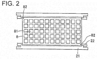
- Fig. 2 is a plan view of the carrier member 8 positioned at the working position.
- the carrier member 8 is formed in a rectangular plate shape by using a resin or the like.
- the carrier member 8 has multiple concave cavity sections 81 having a shallow bottom, and accommodates one individual board 85 in each cavity section 81.
- the approximately square cavity sections 81 are arranged in a two-dimensional lattice pattern of 5 rows and 11 columns.
- a position fiducial mark 82 is attached to each of two corners positioned on a diagonal line of the carrier member 8.
- the carrier conveyance device 2 is configured with a backup device (not shown in Fig. 1 ) and the like such as a pair of guide rails 21 and a pair of conveyor belts 22.
- the pair of guide rails 21 extend in a conveyance direction (X-axis direction) across the center of an upper face of the device table 9, and is assembled on the device table 9 in parallel to each other.
- the pair of endless annular conveyor belts 22 are arranged on an inner side of the pair of guide rails 21 facing each other.
- the pair of conveyor belts 22 rotate in a state where edges of two opposite sides of the carrier member 8 are placed on a conveyor conveyance surface, and performs loading and unloading.
- the backup device is disposed below the working position. The backup device pushes up the carrier member 8 to clamp it in a horizontal posture and positions it.
- the board lifting-up device 3 is an XY-robot type device which can be horizontally moved in an X-axis direction and a Y-axis direction.
- the board lifting-up device 3 not only lifts up the individual board 85 but also transfers it.
- the board lifting-up device 3 is configured with a pair of Y-axis rails 31 and a Y-axis slider 33, a work head 34, a nozzle tool 35, a suction nozzle 36, a position detecting camera 37, and the like configuring a head driving mechanism.
- the pair of Y-axis rails 31 are arranged near both side faces of the device table 9, and extends in a front-rear direction (Y-axis direction).
- the Y-axis slider 33 is movably mounted on the pair of Y-axis rails 31.
- the Y-axis slider 33 is driven in the Y-axis direction by a Y-axis ball screw mechanism (not shown).
- the work head 34 is movably mounted on the Y-axis slider 33.
- the work head 34 is driven in the X-axis direction an X-axis ball screw mechanism (not shown).
- the nozzle tool 35 is exchangeably held at the work head 34.
- the nozzle tool 35 includes the suction nozzle 36 on a lower side.
- the suction nozzle 36 sucks and lifts up an upper face of the individual board 85 by using negative pressure.
- the present invention is not limited thereto, and the nozzle tool 35 may have a clamping chuck that nips and lifts up the individual board 85.
- the position detecting camera 37 is disposed on the work head 34 by being implemented in parallel with the nozzle tool 35.
- the position detecting camera 37 images the position fiducial mark 82 attached to the carrier member 8 and detects an accurate position of the carrier member 8.
- the three-dimensional coplanarity inspection device 4 (hereafter, it is abbreviated as inspection device 4) is provided on an upper face of the device table 9 of the front side of the carrier conveyance device 2.
- the inspection device 4 is disposed upward and inspects a lower surface of the individual board 85 from below.
- the inspection device 4 is an embodiment of a flatness inspection device of the present invention which determines whether or not to use it by inspecting flatness of the lifted individual board 85.
- the flatness inspection device is not limited to the three-dimensional coplanarity inspection device 4, but may be a scan type flatness inspection device which horizontally moves the individual board 85 at a position above a height detecting section and detects the height of each section of the individual board 85.
- the board supplying device 5 is provided on an upper face of the device table 9 of the front side of the inspection device 4.
- the board supplying device 5 includes a pallet conveyance mechanism (not shown) that loads and unloads a tray 51 on which multiple individual boards 85 are placed and a pallet on which the tray 51 is placed.
- the tray 51 includes multiple cavity sections 52 for accommodating the individual boards 85 one by one. Multiple trays 51 are stacked and placed on the pallet.
- the upper tray 51 is collected when whole individual boards 85 are used and become empty. With this, the lower tray 51 accommodating the individual board 85 in each cavity section 52 can be used.
- a collection tray 59 is disposed on an upper face of the device table 9 near the inspection device 4 and the board supplying device 5.
- the collection tray 59 on which the individual board 85 determined to be unusable by the inspection device 4 is placed is collected by an operator.
- the control device 6 is assembled to the device table 9, and its installation position is not particularly limited.
- the control device 6 controls an operation of the carrier conveyance device 2, the board lifting-up device 3, the inspection device 4, and the board supplying device 5.
- the control device 6 includes a display section that displays information to an operator, an input section that can input setting by the operator, and a communication section that exchanges information with other control devices. A control function of the control device 6 will be described together with an operation of the board inspection machine 1.
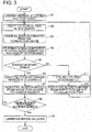
- Fig. 3 is an operation flow diagram of the board inspection machine 1 of the first embodiment.
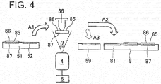
- Fig. 4 is a side view schematically explaining an operation of the board inspection machine 1 of the first embodiment. The operation of the board inspection machine 1 is mainly progressed by a control function the control device 6.
- step S1 of Fig. 3 in accordance with an instruction from the control device 6, the carrier conveyance device 2 loads the empty carrier member 8 and positions it at the working position.
- step S2 the control device 6 designates the tray 51 or the cavity section 52 and instructs the designated result to the board lifting-up device 3.
- step S3 the board lifting-up device 3 moves the suction nozzle 36 above the designated cavity section 52, and sucks and lifts up the individual board 85 from the cavity section 52.
- the board lifting-up device 3 transfers the individual board 85 by moving the suction nozzle 36 above the inspection device 4.
- An operation of the board lifting-up device 3 in step S3 is illustrated by an arrow A1 in Fig. 4 .
- step S4 the inspection device 4 inspects the flatness of the individual board 85 and determines whether or not it can be used in accordance with an instruction from the control device 6. More specifically, the inspection device 4 is the three-dimensional coplanarity inspection device 4 that performs imaging at an upward imaging view angle ⁇ illustrated in Fig. 4 . Then, within a range of the imaging view angle ⁇ , the whole individual boards 85 lifted by the suction nozzle 36 are contained. The inspection device 4 images a back side face 87 of the individual board 85 by one image, and inspects the coplanarities of multiple predetermined positions of the individual boards 85.
- the inspection device 4 performs image analysis with respect to a captured image, and inspects whether or not multiple predetermined positions of the individual boards 85 are approximately within one plane.
- the inspection device 4 determines that the individual board 85 is usable when the flatness is good that the multiple positions are within one plane, and determines that the individual board 85 is unusable when the flatness is not good.
- the inspection device 4 transfers an inspection determination result to the control device 6.
- step S5 if the inspection determination result is usable, an operation flow of the control device 6 proceeds to step S6, and if the inspection determination result is unusable, the operation flow of the control device 6 proceeds to step S11.
- step S6 the control device 6 designates the carrier member 8 or the cavity section 81, and instructs the designated result to the board lifting-up device 3.
- step S7 the board lifting-up device 3 moves the suction nozzle 36 from above of the inspection device 4 to above of the designated cavity section 81, and places the individual board 85 on the designated cavity section 81.
- An operation of the board lifting-up device 3 of step S7 is illustrated by an arrow A2 of Fig. 4 .
- the movement of one individual board 85 is completed by a series of operations from step S2 to step S7.
- step S8 the control device 6 determines whether or not it is in a fully loaded state in which the individual boards 85 are placed in whole cavity sections 81 of the carrier member 8. When it is not in the fully loaded state, the operation flow of the control device 6 returns to step S2, and starts the movement of the next individual board 85.
- positions of the cavity sections 52 of the tray 51 and positions of the cavity sections 81 of the carrier member 8 are sequentially changed and designated.
- the carrier member 8 is in the fully loaded state where the individual boards 85 are accommodated in whole cavity sections 81.
- step S9 the carrier conveyance device 2 unloads the carrier member 8 of the fully loaded state in the solder printing machine 10.
- control device 6 designates the collection tray 59, and instructs the designated result to the board lifting-up device 3 in step S11 which is advanced when the inspection determination result in step S5 is unusable.
- step S12 the board lifting-up device 3 moves the suction nozzle 36 from above of the inspection device 4 to above of the collection tray 59, and places the unusable individual board 85 on the collection tray 59.
- An operation of the board lifting-up device 3 of step S12 is illustrated by a dashed arrow A3 of Fig. 4 .
- the operation flow of the control device 6 returns to step S2, and the movement of the next individual board 85 starts.
- the unusable individual board 85 collected by the collection tray 59 is repaired and provided to be used, and discarded when it is hard to repair.
- the board inspection machine 1 of the first embodiment includes the carrier conveyance device 2 that loads, positions, and unloads the carrier member 8 on which multiple the individual boards 85 on which components are mounted by printing solder paste are placed, the board lifting-up device 3 that lifts up the individual board 85, and the three-dimensional coplanarity inspection device 4 (flatness inspection device) that inspects the flatness of the lifted individual board 85 and determines whether or not usability the individual board 85.
- the carrier conveyance device 2 that loads, positions, and unloads the carrier member 8 on which multiple the individual boards 85 on which components are mounted by printing solder paste are placed
- the board lifting-up device 3 that lifts up the individual board 85
- the three-dimensional coplanarity inspection device 4 flatness inspection device
- the multiple individual boards 85 are sequentially lifted by the board lifting-up device 3 and the flatness can be sequentially inspected by the inspection device 4, efficient inspection is performed.
- the full inspection is performed with respect to the flatness of the multiple individual boards 85, the quality of the individual board 85 is improved.
- the board inspection machine 1 of the first embodiment further includes the board supplying device 5 that moves the individual board 85 on the tray 51 and supplies the individual board 85, the board lifting-up device 3 places the individual board 85 lifted from the tray 51 on the carrier member 8 positioned through the inspection device 4, and the inspection device 4 inspects the flatness of the individual board 85 during moving. According to this, since inspection of the flatness required in the related art is performed during a movement operation for the individual board 85, an inspection time is efficient without prolonging.
- the board lifting-up device 3 moves only the individual board 85 determined to be used by the inspection device 4 on the carrier member 8. According to this, the individual board 85 determined to be unusable is not placed on the carrier member 8, and not conveyed to a downstream side process. Meanwhile, in the related art, when the individual board 85 is moved from the tray 51 to the carrier member 8, the inspection of the flatness is not performed. Alternatively, after components are mounted by conveyance the whole individual boards 85 to the downstream side process, inspection of a mounting state of the component and the inspection of the flatness of the individual board 85 are performed at the same time. Therefore, if the flatness of the individual board 85 is not good, waste of components and the individual board 85 occurs. However, in the first embodiment, since the individual board 85 determined to be unusable is collected and repaired, the waste of components and the individual board 85 does not occur.
- the flatness inspection device is the three-dimensional coplanarity inspection device 4 which inspects the coplanarity of multiple predetermined positions of the individual boards 85 by imaging the back side face 87 of the individual board 85 as one image. According to this, since it is a method in which the image analysis is performed after one image is captured, it is more efficient than a scan type flatness inspection device or the like in that it is performed during a short inspection time.
- Fig. 5 is a plan view schematically illustrating a configuration of the board inspection machine 1A of the second embodiment.
- the board inspection machine 1A of the second embodiment includes a board inverting section 7 without including the board supplying device 5 and the collection tray 59.
- the board inverting section 7 is disposed on the upper face of the device table 9 near the carrier conveyance device 2 and the three-dimensional coplanarity inspection device 4.
- the board inverting section 7 inverts the front side face 86 and the back side face 87 of the individual board 85 such that the front side face 86 of the individual board 85 is inspected.
- the board inverting section 7 can be configured by appropriately applying a known technology.
- a control device 6A of the second embodiment has a control function different from that of the control device 6 of the first embodiment.
- Fig. 6 is an operation flow diagram of the board inspection machine 1A of the second embodiment.
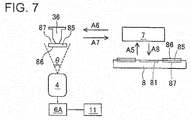
- Fig. 7 is a side view schematically explaining an operation of the board inspection machine 1A of the second embodiment. An operation of the board inspection machine 1A proceeds mainly by a control function of the control device 6A.
- step S21 of Fig. 6 the carrier conveyance device 2 loads the carrier member 8 of the fully loaded state on which respective individual boards 85 are accommodated in the cavity sections 81 in accordance with an instruction from the control device 6A, and positions the carrier member 8 on the working position.
- the control device 6A designates a certain cavity section 81 of the carrier member 8, and instructs the designated result to the board lifting-up device 3.
- the board lifting-up device 3 moves the suction nozzle 36 above of the designated cavity sections 81, and absorbs and lifts up the individual board 85 from the designated cavity sections 81.
- the board lifting-up device 3 moves the suction nozzle 36 to the board inverting section 7, and places the individual board 85 in the board inverting section 7 (see arrow A5 of Fig. 7 ).
- step S24 the board inverting section 7 inverts the front side face 86 and the back side face 87 of the individual board 85.
- step S25 the board lifting-up device 3 sucks and lifts up the individual board 85 from the board inverting section 7, and moves the suction nozzle 36 above the inspection device 4 (see arrow A6 Fig. 7 ).
- step S26 in accordance with an instruction from the control device 6A, the inspection device 4 inspects the flatness of the front side face 86 under the individual board 85 and determines whether or not to use it. With this, since the front side face 86 on which components are actually mounted can be inspected, a detection accuracy of the flatness is improved.
- the inspection device 4 transmits the inspection determination result to the control device 6A.
- step S27 the board lifting-up device 3 moves the suction nozzle 36 to the board inverting section 7, and places the individual board 85 on which the inspection is completed on the board inverting section 7 (see arrow A7 of Fig. 7 ).
- step S28 the board inverting section 7 inverts the back side face 87 and the front side face 86 of the individual board 85.
- step S29 the board lifting-up device 3 moves the suction nozzle 36 above the designated original cavity section 81 by sucking and lifting up the individual board 85 from the board inverting section 7.
- the board lifting-up device 3 places the individual board 85 on the original cavity section 81 in a posture positioned on the front side face 86 by returning the individual board 85 (see arrow A8 of Fig. 7 ).
- step S30 if the inspection determination result is usable, the operation flow of the control device 6 proceeds to step S32, and if the inspection determination result is unusable, the operation flow proceeds to step S31.
- step S31 the control device 6 stores the position of the cavity section 81 in which the individual board 85 determined to be unusable is accommodated, and causes the operation flow to be merged with step S32. At the series of the operations from step S22 to step S31, the inspection on one individual board 85 is completed.
- step S32 the control device 6 determines whether or not the inspection on the whole individual boards 85 above the carrier member 8 is completed. When it is not completed, the operation flow of the control device 6 returns to step S22, and the inspection on the next individual board 85 starts. By repeating the series of the operations from step S22 to step S32, the positions of the cavity sections 81 of the carrier member 8 are sequentially changed and designated. The inspection on the whole individual boards 85 of the cavity sections 81 that are arranged in 5 rows and 11 columns is completed at 55 times, Then, the operation flow of the control device 6 proceeds from step S32 to step S33, and exits from the iteration loop.
- step S33 the carrier conveyance device 2 unloads the carrier member 8 to the solder printing machine 10.
- step S34 the control device 6 transmits the position of the cavity section 81 stored in step S31 to a downstream side process. In other words, the control device 6 transmits the position of the cavity section 81 in which the individual board 85 determined to be unusable is accommodated to the downstream side process. There are cases where there are multiple positions of corresponding cavity sections 81, and there are cases where there are none.
- a destination address of the position of the cavity section 81 is set to a control section of a component mounting machine 11 in a downstream side of the solder printing machine 10.
- a transmission route is not limited to a direct route from the control device 6 to the component mounting machine 11, and may be an indirect route through the solder printing machine 10 or through a higher host computer.
- a control function in step S34 of the control device 6A corresponds to a position transmitting section of the present invention.
- solder paste is printed on whole individual boards 85 irrespective of usability. Furthermore, in the component mounting machine 11 of the downstream side, a component is mounted on only the individual board 85 determined to be usable. In the second embodiment, the individual board 85 different from the first embodiment determined to be unusable is not collected. For this reason, when the individual board 85 is collected, solder printing is performed in a state where the cavity sections 81 of a part of the carrier member 8 are empty such that the flatness of a screen used in the printing becomes unstable, and the solder is additionally leaked to the empty cavity section 81.
- the carrier conveyance device 2 loads and positions the carrier member 8 on which the multiple the individual boards 85 are placed, and the board lifting-up device 3 lifts up the individual board 85 from the positioned carrier member 8, transports the lifted individual board 85 to the three-dimensional coplanarity inspection device 4 (flatness inspection device), and returns the individual board 85 to the original position on the carrier member 8 when the inspection is completed by the inspection device 4.
- the three-dimensional coplanarity inspection device 4 flatness inspection device
- the board inspection machine 1A of the second embodiment further includes the position transmitting section (control function in step S34 of control device 6A) that transmits the position of the individual board 85 determined to be unusable by the inspection device 4 above the carrier member 8 to the downstream side process.
- the position transmitting section control function in step S34 of control device 6A
- the inspection device 4 performs the inspection below the individual board 85 and further includes the board inverting section 7 that inverts the front side face 86 and the back side face 87 of the individual board 85 so that the front side face 86 of the individual board 85 is inspected. According to this, since the flatness of the front side face 86 for mounting a component on the individual board 85 is inspected, the detection accuracy of the flatness is improved more than the flatness required for the inspection of the back side face 87 and a determination accuracy of the usability is also improved.
- the board inverting section 7 used in the second embodiment can also be incorporated in the board inspection machine 1 of the first embodiment.
- step S3 the individual board 85 passes through the board inverting section 7 during the individual board 85 is moved from the tray 51 to the inspection device 4, and in step S7, the individual board 85 passes through the board inverting section 7 during the individual board 85 is transferred from the inspection device 4 to the carrier member 8.
- step S7 the individual board 85 passes through the board inverting section 7 during the individual board 85 is transferred from the inspection device 4 to the carrier member 8.
- Various applications and modifications can also be applied to the present invention.
- 1, 1A board inspection machine
- 2 carrier conveyance device
- 3 board lifting-up device
- 36 suction nozzle
- 4 three-dimensional coplanarity inspection device (flatness inspection device)
- 5 board supplying device
- 59 collection tray
- 6A control device
- 7 board inverting section
- 8 carrier member
- 81 cavity section
- 9 device table
- 10 solder printing machine
- 11 component mounting machine
Landscapes
- Engineering & Computer Science (AREA)
- General Physics & Mathematics (AREA)
- Physics & Mathematics (AREA)
- Immunology (AREA)
- Health & Medical Sciences (AREA)
- Biochemistry (AREA)
- General Health & Medical Sciences (AREA)
- Chemical & Material Sciences (AREA)
- Life Sciences & Earth Sciences (AREA)
- Pathology (AREA)
- Analytical Chemistry (AREA)
- Operations Research (AREA)
- Manufacturing & Machinery (AREA)
- Microelectronics & Electronic Packaging (AREA)
- Investigating Materials By The Use Of Optical Means Adapted For Particular Applications (AREA)
- Supply And Installment Of Electrical Components (AREA)
- Electric Connection Of Electric Components To Printed Circuits (AREA)
- Length Measuring Devices By Optical Means (AREA)
- Length Measuring Devices With Unspecified Measuring Means (AREA)
Abstract
Description
- The present invention relates to a board inspection machine for inspecting flatness of multiple individual boards placed on a carrier member.
- As equipment for producing a board on which a large number of components are mounted, there are a solder printing machine, a component mounting machine, a reflow machine, a board inspection machine, and the like. It is common to connect this equipment in a row to construct a board production line. Among them, the component mounting machine includes a component transfer device that picks up a component from a component supply device and mounts it on the board loaded in a board conveyance device. Furthermore, there is also the component mounting machine including a coplanarity inspection device for checking a state of terminals of the component. According to this, lead curve of a leaded component, missing bumps or bump defects of a bump component, and the like are detected. One technical example relating to this type of the coplanarity inspection device is disclosed in
PTL 1. - In an electronic component mounting method of
PTL 1, two-dimensional data for positioning is obtained by imaging an electronic component, height data is obtained by imaging an electronic component on which angle correction is performed based on two-dimensional data, and three-dimensional data is finally obtained. According to this, in addition to lead floating inspection, since flatness inspection of electronic components having ball shaped terminals such as BGA and CSP can be performed at high speed and reliably, and a mounting takt time can be remarkably shortened. - PTL 1:
JP-A-2001-60800 - However, in accordance with miniaturization of terminals (leads, bumps) accompanying recent miniaturization of components, quality improvement relating to a mounting operation of the components further becomes necessary. That is, in
PTL 1, flatness of a terminal of an electronic component is inspected. However, this is insufficient, and it is necessary to inspect the flatness of a board side on which the components are mounted. On the other hand, along with miniaturization of boards such as mobile phones, production forms of the boards have diversified. That is, in addition to a general production form in which boards are loaded and unloaded one by one and components are sequentially mounted, a production method in which a multiple board in which multiple small boards are integrated is separated after mounting components and a production method in which a mounting operation is performed in a state where multiple small boards are placed on a carrier member are also increasing. This type of small board is referred to as an individual board or a module board. - The present invention has been made in view of the problems of the above background art, and an object of the present invention is to provide a board inspection machine which can improve quality of individual boards by efficiently inspecting flatness of multiple individual boards placed on a carrier member.
- The board inspection machine of the present invention for solving the problems includes a carrier conveyance device that loads, positions, and unloads a carrier member on which multiple individual boards are placed, solder paste being printed and a component being mounted on the individual board, a board lifting-up device that lifts up the individual board, and a flatness inspection device that inspects flatness of the lifted individual board and determines usability of the individual board.
- According to the board inspection machine of the present invention, since the multiple individual boards are sequentially lifted by the board lifting-up device and the flatness can be sequentially inspected by the flatness inspection device, efficient inspection is performed. In addition, since full inspection is performed with respect to the flatness of the multiple individual boards, quality of the individual board is improved.
-
- [
Fig. 1] Fig. 1 is a plan view schematically illustrating a configuration of a board inspection machine of a first embodiment of the present invention. - [
Fig. 2] Fig. 2 is a plan view of a carrier member positioned at a working position. - [
Fig. 3] Fig. 3 is an operation flow diagram of a board inspection machine of the first embodiment. - [
Fig. 4] Fig. 4 is a side view for schematically explaining an operation of the board inspection machine of the first embodiment. - [
Fig. 5] Fig. 5 is a plan view schematically illustrating a configuration of a board inspection machine of a second embodiment. - [
Fig. 6] Fig. 6 is an operation flow diagram of the board inspection machine of the second embodiment. - [
Fig. 7] Fig. 7 is a side view for schematically explaining an operation of the board inspection machine of the second embodiment. - A configuration of a
board inspection machine 1 of a first embodiment of the present invention will be described with reference toFig. 1. Fig. 1 is a plan view schematically illustrating a configuration of theboard inspection machine 1 of the first embodiment of the present invention. A direction from the left side to the right side inFig. 1 is an X-axis direction through which acarrier member 8 is conveyed. The lower side inFig. 1 is the front side of theboard inspection machine 1, the upper side thereof is the back side, and a direction from the front side to the back side is a Y-axis direction. Theboard inspection machine 1 is disposed in an upstream process of thesolder printing machine 10, and sets anindividual board 85, as an inspection target, before solder paste is printed. Theboard inspection machine 1 is configured by assembling acarrier conveyance device 2, a board lifting-updevice 3, a three-dimensionalcoplanarity inspection device 4, theboard supplying device 5, acontrol device 6, and the like on a device table 9. - The
carrier conveyance device 2 loads thecarrier member 8, positions it at a working position approximately at the center of the device table 9, and unloads it to thesolder printing machine 10.Fig. 2 is a plan view of thecarrier member 8 positioned at the working position. Thecarrier member 8 is formed in a rectangular plate shape by using a resin or the like. Thecarrier member 8 has multipleconcave cavity sections 81 having a shallow bottom, and accommodates oneindividual board 85 in eachcavity section 81. InFig. 2 , the approximatelysquare cavity sections 81 are arranged in a two-dimensional lattice pattern of 5 rows and 11 columns. A position fiducial mark 82 is attached to each of two corners positioned on a diagonal line of thecarrier member 8. - The
carrier conveyance device 2 is configured with a backup device (not shown inFig. 1 ) and the like such as a pair ofguide rails 21 and a pair ofconveyor belts 22. The pair ofguide rails 21 extend in a conveyance direction (X-axis direction) across the center of an upper face of the device table 9, and is assembled on the device table 9 in parallel to each other. The pair of endlessannular conveyor belts 22 are arranged on an inner side of the pair ofguide rails 21 facing each other. The pair ofconveyor belts 22 rotate in a state where edges of two opposite sides of thecarrier member 8 are placed on a conveyor conveyance surface, and performs loading and unloading. The backup device is disposed below the working position. The backup device pushes up thecarrier member 8 to clamp it in a horizontal posture and positions it. - The board lifting-up
device 3 is an XY-robot type device which can be horizontally moved in an X-axis direction and a Y-axis direction. The board lifting-updevice 3 not only lifts up theindividual board 85 but also transfers it. The board lifting-updevice 3 is configured with a pair of Y-axis rails 31 and a Y-axis slider 33, awork head 34, anozzle tool 35, asuction nozzle 36, aposition detecting camera 37, and the like configuring a head driving mechanism. The pair of Y-axis rails 31 are arranged near both side faces of the device table 9, and extends in a front-rear direction (Y-axis direction). The Y-axis slider 33 is movably mounted on the pair of Y-axis rails 31. The Y-axis slider 33 is driven in the Y-axis direction by a Y-axis ball screw mechanism (not shown). - The
work head 34 is movably mounted on the Y-axis slider 33. Thework head 34 is driven in the X-axis direction an X-axis ball screw mechanism (not shown). Thenozzle tool 35 is exchangeably held at thework head 34. Thenozzle tool 35 includes thesuction nozzle 36 on a lower side. Thesuction nozzle 36 sucks and lifts up an upper face of theindividual board 85 by using negative pressure. The present invention is not limited thereto, and thenozzle tool 35 may have a clamping chuck that nips and lifts up theindividual board 85. Theposition detecting camera 37 is disposed on thework head 34 by being implemented in parallel with thenozzle tool 35. Theposition detecting camera 37 images the position fiducial mark 82 attached to thecarrier member 8 and detects an accurate position of thecarrier member 8. - The three-dimensional coplanarity inspection device 4 (hereafter, it is abbreviated as inspection device 4) is provided on an upper face of the device table 9 of the front side of the
carrier conveyance device 2. Theinspection device 4 is disposed upward and inspects a lower surface of theindividual board 85 from below. Theinspection device 4 is an embodiment of a flatness inspection device of the present invention which determines whether or not to use it by inspecting flatness of the liftedindividual board 85. The flatness inspection device is not limited to the three-dimensionalcoplanarity inspection device 4, but may be a scan type flatness inspection device which horizontally moves theindividual board 85 at a position above a height detecting section and detects the height of each section of theindividual board 85. - The
board supplying device 5 is provided on an upper face of the device table 9 of the front side of theinspection device 4. Theboard supplying device 5 includes a pallet conveyance mechanism (not shown) that loads and unloads atray 51 on which multipleindividual boards 85 are placed and a pallet on which thetray 51 is placed. Thetray 51 includesmultiple cavity sections 52 for accommodating theindividual boards 85 one by one.Multiple trays 51 are stacked and placed on the pallet. Theupper tray 51 is collected when wholeindividual boards 85 are used and become empty. With this, thelower tray 51 accommodating theindividual board 85 in eachcavity section 52 can be used. - A
collection tray 59 is disposed on an upper face of the device table 9 near theinspection device 4 and theboard supplying device 5. Thecollection tray 59 on which theindividual board 85 determined to be unusable by theinspection device 4 is placed is collected by an operator. - The
control device 6 is assembled to the device table 9, and its installation position is not particularly limited. Thecontrol device 6 controls an operation of thecarrier conveyance device 2, the board lifting-updevice 3, theinspection device 4, and theboard supplying device 5. Thecontrol device 6 includes a display section that displays information to an operator, an input section that can input setting by the operator, and a communication section that exchanges information with other control devices. A control function of thecontrol device 6 will be described together with an operation of theboard inspection machine 1. - In the
board inspection machine 1 of the first embodiment, anempty carrier member 8 is loaded by thecarrier conveyance device 2, and theindividual board 85 is moved from thetray 51 to thecarrier member 8 by the board lifting-updevice 3. Theinspection device 4 inspects the flatness of theindividual board 85 during moving and lifted by the board lifting-updevice 3 from below.Fig. 3 is an operation flow diagram of theboard inspection machine 1 of the first embodiment. In addition,Fig. 4 is a side view schematically explaining an operation of theboard inspection machine 1 of the first embodiment. The operation of theboard inspection machine 1 is mainly progressed by a control function thecontrol device 6. - In an initial state, it is assumed that the
multiple trays 51 on which theindividual boards 85 are stacked are loaded on theboard supplying device 5 in advance. In step S1 ofFig. 3 , in accordance with an instruction from thecontrol device 6, thecarrier conveyance device 2 loads theempty carrier member 8 and positions it at the working position. In next step S2, thecontrol device 6 designates thetray 51 or thecavity section 52 and instructs the designated result to the board lifting-updevice 3. In step S3, the board lifting-updevice 3 moves thesuction nozzle 36 above the designatedcavity section 52, and sucks and lifts up theindividual board 85 from thecavity section 52. Next, the board lifting-updevice 3 transfers theindividual board 85 by moving thesuction nozzle 36 above theinspection device 4. An operation of the board lifting-updevice 3 in step S3 is illustrated by an arrow A1 inFig. 4 . - In step S4, the
inspection device 4 inspects the flatness of theindividual board 85 and determines whether or not it can be used in accordance with an instruction from thecontrol device 6. More specifically, theinspection device 4 is the three-dimensionalcoplanarity inspection device 4 that performs imaging at an upward imaging view angle θ illustrated inFig. 4 . Then, within a range of the imaging view angle θ, the wholeindividual boards 85 lifted by thesuction nozzle 36 are contained. Theinspection device 4 images aback side face 87 of theindividual board 85 by one image, and inspects the coplanarities of multiple predetermined positions of theindividual boards 85. - That is, the
inspection device 4 performs image analysis with respect to a captured image, and inspects whether or not multiple predetermined positions of theindividual boards 85 are approximately within one plane. Theinspection device 4 determines that theindividual board 85 is usable when the flatness is good that the multiple positions are within one plane, and determines that theindividual board 85 is unusable when the flatness is not good. Theinspection device 4 transfers an inspection determination result to thecontrol device 6. - In step S5, if the inspection determination result is usable, an operation flow of the
control device 6 proceeds to step S6, and if the inspection determination result is unusable, the operation flow of thecontrol device 6 proceeds to step S11. In step S6, thecontrol device 6 designates thecarrier member 8 or thecavity section 81, and instructs the designated result to the board lifting-updevice 3. In step S7, the board lifting-updevice 3 moves thesuction nozzle 36 from above of theinspection device 4 to above of the designatedcavity section 81, and places theindividual board 85 on the designatedcavity section 81. An operation of the board lifting-updevice 3 of step S7 is illustrated by an arrow A2 ofFig. 4 . The movement of oneindividual board 85 is completed by a series of operations from step S2 to step S7. - In step S8, the
control device 6 determines whether or not it is in a fully loaded state in which theindividual boards 85 are placed inwhole cavity sections 81 of thecarrier member 8. When it is not in the fully loaded state, the operation flow of thecontrol device 6 returns to step S2, and starts the movement of the nextindividual board 85. By repeating the series of the operations from step S2 to step S8, positions of thecavity sections 52 of thetray 51 and positions of thecavity sections 81 of thecarrier member 8 are sequentially changed and designated. When the movement of theindividual board 85 to thecavity sections 81 that are arranged in 5 rows and 11 columns is performed 55 times, thecarrier member 8 is in the fully loaded state where theindividual boards 85 are accommodated inwhole cavity sections 81. Then, the operation flow of thecontrol device 6 proceeds from step S8 to step S9, and exits an iteration loop. In step S9, thecarrier conveyance device 2 unloads thecarrier member 8 of the fully loaded state in thesolder printing machine 10. - In addition, the
control device 6 designates thecollection tray 59, and instructs the designated result to the board lifting-updevice 3 in step S11 which is advanced when the inspection determination result in step S5 is unusable. In step S12, the board lifting-updevice 3 moves thesuction nozzle 36 from above of theinspection device 4 to above of thecollection tray 59, and places the unusableindividual board 85 on thecollection tray 59. An operation of the board lifting-updevice 3 of step S12 is illustrated by a dashed arrow A3 ofFig. 4 . Then, the operation flow of thecontrol device 6 returns to step S2, and the movement of the nextindividual board 85 starts. The unusableindividual board 85 collected by thecollection tray 59 is repaired and provided to be used, and discarded when it is hard to repair. - The
board inspection machine 1 of the first embodiment includes thecarrier conveyance device 2 that loads, positions, and unloads thecarrier member 8 on which multiple theindividual boards 85 on which components are mounted by printing solder paste are placed, the board lifting-updevice 3 that lifts up theindividual board 85, and the three-dimensional coplanarity inspection device 4 (flatness inspection device) that inspects the flatness of the liftedindividual board 85 and determines whether or not usability theindividual board 85. - According to this, since the multiple
individual boards 85 are sequentially lifted by the board lifting-updevice 3 and the flatness can be sequentially inspected by theinspection device 4, efficient inspection is performed. In addition, since the full inspection is performed with respect to the flatness of the multipleindividual boards 85, the quality of theindividual board 85 is improved. - Furthermore, the
board inspection machine 1 of the first embodiment further includes theboard supplying device 5 that moves theindividual board 85 on thetray 51 and supplies theindividual board 85, the board lifting-updevice 3 places theindividual board 85 lifted from thetray 51 on thecarrier member 8 positioned through theinspection device 4, and theinspection device 4 inspects the flatness of theindividual board 85 during moving. According to this, since inspection of the flatness required in the related art is performed during a movement operation for theindividual board 85, an inspection time is efficient without prolonging. - Furthermore, the board lifting-up
device 3 moves only theindividual board 85 determined to be used by theinspection device 4 on thecarrier member 8. According to this, theindividual board 85 determined to be unusable is not placed on thecarrier member 8, and not conveyed to a downstream side process. Meanwhile, in the related art, when theindividual board 85 is moved from thetray 51 to thecarrier member 8, the inspection of the flatness is not performed. Alternatively, after components are mounted by conveyance the wholeindividual boards 85 to the downstream side process, inspection of a mounting state of the component and the inspection of the flatness of theindividual board 85 are performed at the same time. Therefore, if the flatness of theindividual board 85 is not good, waste of components and theindividual board 85 occurs. However, in the first embodiment, since theindividual board 85 determined to be unusable is collected and repaired, the waste of components and theindividual board 85 does not occur. - Furthermore, the flatness inspection device is the three-dimensional
coplanarity inspection device 4 which inspects the coplanarity of multiple predetermined positions of theindividual boards 85 by imaging theback side face 87 of theindividual board 85 as one image. According to this, since it is a method in which the image analysis is performed after one image is captured, it is more efficient than a scan type flatness inspection device or the like in that it is performed during a short inspection time. - Next, for a
board inspection machine 1A of a second embodiment, points different from the first embodiment will be mainly described.Fig. 5 is a plan view schematically illustrating a configuration of theboard inspection machine 1A of the second embodiment. Theboard inspection machine 1A of the second embodiment includes aboard inverting section 7 without including theboard supplying device 5 and thecollection tray 59. Theboard inverting section 7 is disposed on the upper face of the device table 9 near thecarrier conveyance device 2 and the three-dimensionalcoplanarity inspection device 4. Theboard inverting section 7 inverts thefront side face 86 and theback side face 87 of theindividual board 85 such that the front side face 86 of theindividual board 85 is inspected. Theboard inverting section 7 can be configured by appropriately applying a known technology. In addition, acontrol device 6A of the second embodiment has a control function different from that of thecontrol device 6 of the first embodiment. - In the
board inspection machine 1A of the second embodiment, thecarrier conveyance device 2 loads thecarrier member 8 on which theindividual boards 85 are fully loaded. The board lifting-updevice 3 transfers and returns theindividual board 85 through theboard inverting section 7 between thecarrier member 8 and theinspection device 4.Fig. 6 is an operation flow diagram of theboard inspection machine 1A of the second embodiment. In addition,Fig. 7 is a side view schematically explaining an operation of theboard inspection machine 1A of the second embodiment. An operation of theboard inspection machine 1A proceeds mainly by a control function of thecontrol device 6A. - In step S21 of
Fig. 6 , thecarrier conveyance device 2 loads thecarrier member 8 of the fully loaded state on which respectiveindividual boards 85 are accommodated in thecavity sections 81 in accordance with an instruction from thecontrol device 6A, and positions thecarrier member 8 on the working position. In step S22, thecontrol device 6A designates acertain cavity section 81 of thecarrier member 8, and instructs the designated result to the board lifting-updevice 3. In step S23 , the board lifting-updevice 3 moves thesuction nozzle 36 above of the designatedcavity sections 81, and absorbs and lifts up theindividual board 85 from the designatedcavity sections 81. Next, the board lifting-updevice 3 moves thesuction nozzle 36 to theboard inverting section 7, and places theindividual board 85 in the board inverting section 7 (see arrow A5 ofFig. 7 ). - In step S24, the
board inverting section 7 inverts thefront side face 86 and theback side face 87 of theindividual board 85. In step S25, the board lifting-updevice 3 sucks and lifts up theindividual board 85 from theboard inverting section 7, and moves thesuction nozzle 36 above the inspection device 4 (see arrow A6Fig. 7 ). In step S26, in accordance with an instruction from thecontrol device 6A, theinspection device 4 inspects the flatness of the front side face 86 under theindividual board 85 and determines whether or not to use it. With this, since the front side face 86 on which components are actually mounted can be inspected, a detection accuracy of the flatness is improved. Furthermore, it is preferable to set pad portions for soldering component terminals as multiple places of theindividual boards 85 of which the flatness is inspected. According to this, the detection accuracy of the flatness is further improved. Theinspection device 4 transmits the inspection determination result to thecontrol device 6A. - In step S27, the board lifting-up
device 3 moves thesuction nozzle 36 to theboard inverting section 7, and places theindividual board 85 on which the inspection is completed on the board inverting section 7 (see arrow A7 ofFig. 7 ). In step S28, theboard inverting section 7 inverts theback side face 87 and the front side face 86 of theindividual board 85. In step S29, the board lifting-updevice 3 moves thesuction nozzle 36 above the designatedoriginal cavity section 81 by sucking and lifting up theindividual board 85 from theboard inverting section 7. Next, the board lifting-updevice 3 places theindividual board 85 on theoriginal cavity section 81 in a posture positioned on the front side face 86 by returning the individual board 85 (see arrow A8 ofFig. 7 ). - In step S30, if the inspection determination result is usable, the operation flow of the
control device 6 proceeds to step S32, and if the inspection determination result is unusable, the operation flow proceeds to step S31. In step S31, thecontrol device 6 stores the position of thecavity section 81 in which theindividual board 85 determined to be unusable is accommodated, and causes the operation flow to be merged with step S32. At the series of the operations from step S22 to step S31, the inspection on oneindividual board 85 is completed. - In step S32, the
control device 6 determines whether or not the inspection on the wholeindividual boards 85 above thecarrier member 8 is completed. When it is not completed, the operation flow of thecontrol device 6 returns to step S22, and the inspection on the nextindividual board 85 starts. By repeating the series of the operations from step S22 to step S32, the positions of thecavity sections 81 of thecarrier member 8 are sequentially changed and designated. The inspection on the wholeindividual boards 85 of thecavity sections 81 that are arranged in 5 rows and 11 columns is completed at 55 times, Then, the operation flow of thecontrol device 6 proceeds from step S32 to step S33, and exits from the iteration loop. - In step S33, the
carrier conveyance device 2 unloads thecarrier member 8 to thesolder printing machine 10. In the next step S34, thecontrol device 6 transmits the position of thecavity section 81 stored in step S31 to a downstream side process. In other words, thecontrol device 6 transmits the position of thecavity section 81 in which theindividual board 85 determined to be unusable is accommodated to the downstream side process. There are cases where there are multiple positions of correspondingcavity sections 81, and there are cases where there are none. - In the second embodiment, a destination address of the position of the
cavity section 81 is set to a control section of acomponent mounting machine 11 in a downstream side of thesolder printing machine 10. A transmission route is not limited to a direct route from thecontrol device 6 to thecomponent mounting machine 11, and may be an indirect route through thesolder printing machine 10 or through a higher host computer. A control function in step S34 of thecontrol device 6A corresponds to a position transmitting section of the present invention. - Then, in the
solder printing machine 10 of the downstream side, solder paste is printed on wholeindividual boards 85 irrespective of usability. Furthermore, in thecomponent mounting machine 11 of the downstream side, a component is mounted on only theindividual board 85 determined to be usable. In the second embodiment, theindividual board 85 different from the first embodiment determined to be unusable is not collected. For this reason, when theindividual board 85 is collected, solder printing is performed in a state where thecavity sections 81 of a part of thecarrier member 8 are empty such that the flatness of a screen used in the printing becomes unstable, and the solder is additionally leaked to theempty cavity section 81. - In the
board inspection machine 1A of the second embodiment, thecarrier conveyance device 2 loads and positions thecarrier member 8 on which the multiple theindividual boards 85 are placed, and the board lifting-updevice 3 lifts up theindividual board 85 from the positionedcarrier member 8, transports the liftedindividual board 85 to the three-dimensional coplanarity inspection device 4 (flatness inspection device), and returns theindividual board 85 to the original position on thecarrier member 8 when the inspection is completed by theinspection device 4. According to this, even in a configuration in which theindividual boards 85 are placed on thecarrier member 8 from the beginning, since the flatness can be sequentially inspected, efficient inspection is performed. In addition, since the full inspection is performed with respect to the flatness of the multipleindividual boards 85, the quality of theindividual board 85 is improved. - Furthermore, the
board inspection machine 1A of the second embodiment further includes the position transmitting section (control function in step S34 ofcontrol device 6A) that transmits the position of theindividual board 85 determined to be unusable by theinspection device 4 above thecarrier member 8 to the downstream side process. According to this, in thecomponent mounting machine 11 of the downstream side, since a component can be mounted on only theindividual board 85 determined to be usable, waste of the component does not occur. - Furthermore, the
inspection device 4 performs the inspection below theindividual board 85 and further includes theboard inverting section 7 that inverts thefront side face 86 and theback side face 87 of theindividual board 85 so that the front side face 86 of theindividual board 85 is inspected. According to this, since the flatness of the front side face 86 for mounting a component on theindividual board 85 is inspected, the detection accuracy of the flatness is improved more than the flatness required for the inspection of theback side face 87 and a determination accuracy of the usability is also improved. - The
board inverting section 7 used in the second embodiment can also be incorporated in theboard inspection machine 1 of the first embodiment. In this case, in step S3, theindividual board 85 passes through theboard inverting section 7 during theindividual board 85 is moved from thetray 51 to theinspection device 4, and in step S7, theindividual board 85 passes through theboard inverting section 7 during theindividual board 85 is transferred from theinspection device 4 to thecarrier member 8. Various applications and modifications can also be applied to the present invention. - 1, 1A: board inspection machine, 2: carrier conveyance device, 3: board lifting-up device, 36: suction nozzle, 4: three-dimensional coplanarity inspection device (flatness inspection device), 5: board supplying device, 51: tray, 52: cavity section, 59: collection tray, 6, 6A: control device, 7: board inverting section, 8: carrier member, 81: cavity section, 85: individual board, 86: front side face, 87: back side face, 9: device table, 10: solder printing machine, 11: component mounting machine
Claims (8)
- A board inspection machine comprising:a carrier conveyance device that loads, positions, and unloads a carrier member on which multiple individual boards are placed, solder paste being printed and a component being mounted on the individual boards;a board lifting-up device that lifts up the individual board; anda flatness inspection device that inspects flatness of the lifted individual board and determines usability of the individual board.
- The board inspection machine of Claim 1, further comprising:a board supplying device that moves the individual board on a tray and supplies the moved individual board,wherein the board lifting-up device lifts up the individual board from the tray and transfers the lifted individual board on the positioned carrier member through the flatness inspection device, andthe flatness inspection device inspects the flatness of the individual board during transfer.
- The board inspection machine of Claim 2,
wherein the board lifting-up device moves only the individual board determined to be usable by the flatness inspection device on the carrier member. - The board inspection machine of Claim 1,
wherein the carrier conveyance device loads and positions the carrier member on which multiple individual boards are placed, and
the board lifting-up device lifts up the individual board from the positioned carrier member and transports the individual board to the flatness inspection device, and returns the individual board to an original position on the carrier member when inspection is completed by the flatness inspection device. - The board inspection machine of Claim 4, further comprising:
a position transmitting section transmits a position on the carrier member of the individual board determined to be unusable in the flatness inspection device, to a downstream side process. - The board inspection machine of any one of Claims 1 to 5,
wherein the flatness inspection device performs inspection from below the individual board and further includes a board inverting section that inverts a front side face and a back side face of the individual board such that the front side face of the individual board is inspected. - The board inspection machine of any one of Claims 1 to 6,
wherein the flatness inspection device is a three-dimensional coplanarity inspection device which inspects coplanarity of multiple predetermined positions of the individual boards by imaging the front side face or back side face of the individual board as one image. - The board inspection machine of any one of Claims 1 to 7,
wherein the board inspection machine is disposed in an upstream process of a solder printing machine in which the solder paste is printed on the individual board.
Applications Claiming Priority (1)
| Application Number | Priority Date | Filing Date | Title |
|---|---|---|---|
| PCT/JP2015/068274 WO2016208019A1 (en) | 2015-06-24 | 2015-06-24 | Substrate inspecting apparatus |
Publications (3)
| Publication Number | Publication Date |
|---|---|
| EP3315903A4 EP3315903A4 (en) | 2018-05-02 |
| EP3315903A1 true EP3315903A1 (en) | 2018-05-02 |
| EP3315903B1 EP3315903B1 (en) | 2019-12-18 |
Family
ID=57586526
Family Applications (1)
| Application Number | Title | Priority Date | Filing Date |
|---|---|---|---|
| EP15896341.3A Active EP3315903B1 (en) | 2015-06-24 | 2015-06-24 | Board inspection apparatus |
Country Status (5)
| Country | Link |
|---|---|
| US (1) | US10551181B2 (en) |
| EP (1) | EP3315903B1 (en) |
| JP (1) | JP6527228B2 (en) |
| CN (1) | CN108027234A (en) |
| WO (1) | WO2016208019A1 (en) |
Families Citing this family (2)
| Publication number | Priority date | Publication date | Assignee | Title |
|---|---|---|---|---|
| JP7140930B1 (en) * | 2022-03-07 | 2022-09-21 | Ckd株式会社 | Board inspection device and board inspection method |
| CN219434671U (en) * | 2023-06-29 | 2023-07-28 | 苏州康代智能科技股份有限公司 | Circuit board transmission device, image capturing device and optical detection equipment |
Family Cites Families (32)
| Publication number | Priority date | Publication date | Assignee | Title |
|---|---|---|---|---|
| DE3474750D1 (en) * | 1983-11-05 | 1988-11-24 | Zevatech Ag | Method and device positioning elements on a work piece |
| JPS63260129A (en) * | 1987-04-17 | 1988-10-27 | Hitachi Electronics Eng Co Ltd | Aligner |
| US5561696A (en) * | 1987-10-30 | 1996-10-01 | Hewlett-Packard Company | Method and apparatus for inspecting electrical connections |
| US4959898A (en) * | 1990-05-22 | 1990-10-02 | Emhart Industries, Inc. | Surface mount machine with lead coplanarity verifier |
| JP2750226B2 (en) * | 1991-02-19 | 1998-05-13 | 大日本スクリーン製造株式会社 | How to set the binarization threshold |
| US5991435A (en) * | 1992-06-30 | 1999-11-23 | Matsushita Electric Industrial Co., Ltd. | Inspecting apparatus of mounting state of component or printing state of cream solder in mounting line of electronic component |
| JP3261770B2 (en) * | 1992-11-19 | 2002-03-04 | 松下電器産業株式会社 | Component mounting device |
| US5628110A (en) * | 1994-07-15 | 1997-05-13 | Matsushita Electric Industrial Co., Ltd. | Inspecting method of an electronic component during a mounting operation of the same onto a substrate |
| EP0776151A4 (en) * | 1994-08-08 | 1999-08-11 | Kobe Steel Ltd | Method and apparatus for soldering inspection of circuit board |
| US6118538A (en) * | 1995-01-13 | 2000-09-12 | Cyberoptics Corporation | Method and apparatus for electronic component lead measurement using light based sensors on a component placement machine |
| JPH09130084A (en) * | 1995-11-06 | 1997-05-16 | Matsushita Electric Ind Co Ltd | Component mounting equipment and component mounting equipment |
| US6246789B1 (en) * | 1997-08-29 | 2001-06-12 | Matsushita Electric Industrial Co., Ltd. | Component mounting apparatus and method |
| JPH11220298A (en) * | 1998-02-02 | 1999-08-10 | Matsushita Electric Ind Co Ltd | Electronic component mounting method |
| EP1089607B1 (en) * | 1998-02-27 | 2006-11-22 | Matsushita Electric Industrial Co., Ltd. | Component recognizing method and apparatus |
| KR100364559B1 (en) * | 1998-09-17 | 2002-12-12 | 주식회사 뷰웰 | Ic lead inspection system |
| JP2000196300A (en) * | 1998-12-28 | 2000-07-14 | Matsushita Electric Ind Co Ltd | Object recognition and placement device |
| KR100311747B1 (en) * | 1999-08-20 | 2001-10-18 | 정문술 | PCB Transfering System of Surface Mounting Device |
| JP4315536B2 (en) | 1999-08-24 | 2009-08-19 | Juki株式会社 | Electronic component mounting method and apparatus |
| JP4607313B2 (en) * | 2000-12-08 | 2011-01-05 | 富士機械製造株式会社 | Electronic component mounting system |
| JP2002185103A (en) * | 2000-12-18 | 2002-06-28 | Kyocera Corp | Method for evaluating flatness of electrode pads on mounting surface of mounting substrate |
| KR100936903B1 (en) * | 2007-09-20 | 2010-01-15 | 아주하이텍(주) | Inspection device and inspection method |
| JP2009200247A (en) * | 2008-02-21 | 2009-09-03 | Dap Technology Kk | Packing method and packing apparatus |
| JP5323581B2 (en) * | 2009-05-08 | 2013-10-23 | 三星ディスプレイ株式會社 | Vapor deposition method and vapor deposition apparatus |
| JP5590530B2 (en) * | 2010-08-03 | 2014-09-17 | 富士機械製造株式会社 | PCB printing system |
| JP2012129434A (en) * | 2010-12-17 | 2012-07-05 | Fuji Mach Mfg Co Ltd | Work machine for board |
| WO2012117466A1 (en) * | 2011-03-02 | 2012-09-07 | パナソニック株式会社 | Component mounting device, component mounting method, imaging device, and imaging method |
| CN102288119B (en) * | 2011-06-27 | 2012-11-07 | 上海卓晶半导体科技有限公司 | Device for automatically detecting flatness and thickness of substrates and separating substrates |
| JP5791408B2 (en) * | 2011-07-15 | 2015-10-07 | 富士機械製造株式会社 | Electronic component mounting equipment |
| CN202356323U (en) * | 2011-11-10 | 2012-08-01 | 旭丽电子(广州)有限公司 | Test system for circuit board |
| US9801317B2 (en) * | 2013-03-14 | 2017-10-24 | Fuji Machine Mfg. Co., Ltd. | Production management system for component mounting machine |
| JP6224348B2 (en) * | 2013-05-15 | 2017-11-01 | ヤマハ発動機株式会社 | Judgment device, surface mounter |
| CN103776397A (en) * | 2013-11-22 | 2014-05-07 | 大连世佳精工机械有限公司 | Substrate flatness detection apparatus |
-
2015
- 2015-06-24 US US15/735,419 patent/US10551181B2/en active Active
- 2015-06-24 CN CN201580081008.8A patent/CN108027234A/en active Pending
- 2015-06-24 EP EP15896341.3A patent/EP3315903B1/en active Active
- 2015-06-24 WO PCT/JP2015/068274 patent/WO2016208019A1/en not_active Ceased
- 2015-06-24 JP JP2017524512A patent/JP6527228B2/en active Active
Also Published As
| Publication number | Publication date |
|---|---|
| WO2016208019A1 (en) | 2016-12-29 |
| EP3315903A4 (en) | 2018-05-02 |
| JP6527228B2 (en) | 2019-06-05 |
| CN108027234A (en) | 2018-05-11 |
| EP3315903B1 (en) | 2019-12-18 |
| US20180135976A1 (en) | 2018-05-17 |
| US10551181B2 (en) | 2020-02-04 |
| JPWO2016208019A1 (en) | 2018-04-19 |
Similar Documents
| Publication | Publication Date | Title |
|---|---|---|
| JP3965288B2 (en) | Substrate work result inspection device | |
| JP4767995B2 (en) | Component mounting method, component mounting machine, mounting condition determining method, mounting condition determining apparatus, and program | |
| CN103515274B (en) | Solder ball printing mounting device | |
| CN202799576U (en) | Installed component checking device | |
| CN104111037B (en) | Apparatus for inspecting solder printing | |
| JP6047760B2 (en) | Component mounting system and component mounting method | |
| WO2016181437A1 (en) | Component mounting machine, and component supply method for component mounting machine | |
| CN100584151C (en) | Substrate Manufacturing Equipment for Component Mounting | |
| KR101120129B1 (en) | Method of adjusting work position automatically by reference value and automatic apparatus for the same | |
| JP6694778B2 (en) | Screen printer | |
| EP3315903B1 (en) | Board inspection apparatus | |
| JP4852456B2 (en) | Mounting line and mounting method | |
| JP5927504B2 (en) | Component mounting system and component mounting method | |
| KR101542865B1 (en) | Pre-Bonding Apparatus for Flat Display Panel | |
| JP2014041892A (en) | Screen printing system and screen printing method | |
| TWI467197B (en) | An electronic component operating unit for an image capturing device, and a working device for its application | |
| JP5711074B2 (en) | Component mounting method and component mounting machine | |
| KR102510457B1 (en) | Apparatus and method for surface mounting | |
| KR100531230B1 (en) | Ball mounting system | |
| JP2014041893A (en) | Electronic component mounting system and electronic component mounting unit and electronic component mounting method | |
| JP2004319943A (en) | Component mounting device and component mounting method | |
| WO2024062635A1 (en) | Testing device and testing method | |
| JP4743059B2 (en) | Electronic component mounting system and electronic component mounting method | |
| JP2003152397A (en) | Electric component mounting system and electric circuit manufacturing method | |
| US20180284732A1 (en) | Required accuracy setting device |
Legal Events
| Date | Code | Title | Description |
|---|---|---|---|
| STAA | Information on the status of an ep patent application or granted ep patent |
Free format text: STATUS: THE INTERNATIONAL PUBLICATION HAS BEEN MADE |
|
| PUAI | Public reference made under article 153(3) epc to a published international application that has entered the european phase |
Free format text: ORIGINAL CODE: 0009012 |
|
| STAA | Information on the status of an ep patent application or granted ep patent |
Free format text: STATUS: REQUEST FOR EXAMINATION WAS MADE |
|
| 17P | Request for examination filed |
Effective date: 20171221 |
|
| A4 | Supplementary search report drawn up and despatched |
Effective date: 20180328 |
|
| AK | Designated contracting states |
Kind code of ref document: A1 Designated state(s): AL AT BE BG CH CY CZ DE DK EE ES FI FR GB GR HR HU IE IS IT LI LT LU LV MC MK MT NL NO PL PT RO RS SE SI SK SM TR |
|
| AX | Request for extension of the european patent |
Extension state: BA ME |
|
| DAV | Request for validation of the european patent (deleted) | ||
| DAX | Request for extension of the european patent (deleted) | ||
| RAP1 | Party data changed (applicant data changed or rights of an application transferred) |
Owner name: FUJI CORPORATION |
|
| RIN1 | Information on inventor provided before grant (corrected) |
Inventor name: YAMAKAGE YUSUKE |
|
| GRAP | Despatch of communication of intention to grant a patent |
Free format text: ORIGINAL CODE: EPIDOSNIGR1 |
|
| STAA | Information on the status of an ep patent application or granted ep patent |
Free format text: STATUS: GRANT OF PATENT IS INTENDED |
|
| INTG | Intention to grant announced |
Effective date: 20190905 |
|
| GRAS | Grant fee paid |
Free format text: ORIGINAL CODE: EPIDOSNIGR3 |
|
| GRAA | (expected) grant |
Free format text: ORIGINAL CODE: 0009210 |
|
| STAA | Information on the status of an ep patent application or granted ep patent |
Free format text: STATUS: THE PATENT HAS BEEN GRANTED |
|
| AK | Designated contracting states |
Kind code of ref document: B1 Designated state(s): AL AT BE BG CH CY CZ DE DK EE ES FI FR GB GR HR HU IE IS IT LI LT LU LV MC MK MT NL NO PL PT RO RS SE SI SK SM TR |
|
| REG | Reference to a national code |
Ref country code: CH Ref legal event code: EP |
|
| REG | Reference to a national code |
Ref country code: DE Ref legal event code: R096 Ref document number: 602015044104 Country of ref document: DE |
|
| REG | Reference to a national code |
Ref country code: IE Ref legal event code: FG4D |
|
| REG | Reference to a national code |
Ref country code: AT Ref legal event code: REF Ref document number: 1215084 Country of ref document: AT Kind code of ref document: T Effective date: 20200115 |
|
| REG | Reference to a national code |
Ref country code: NL Ref legal event code: FP |
|
| PG25 | Lapsed in a contracting state [announced via postgrant information from national office to epo] |
Ref country code: NO Free format text: LAPSE BECAUSE OF FAILURE TO SUBMIT A TRANSLATION OF THE DESCRIPTION OR TO PAY THE FEE WITHIN THE PRESCRIBED TIME-LIMIT Effective date: 20200318 Ref country code: GR Free format text: LAPSE BECAUSE OF FAILURE TO SUBMIT A TRANSLATION OF THE DESCRIPTION OR TO PAY THE FEE WITHIN THE PRESCRIBED TIME-LIMIT Effective date: 20200319 Ref country code: LV Free format text: LAPSE BECAUSE OF FAILURE TO SUBMIT A TRANSLATION OF THE DESCRIPTION OR TO PAY THE FEE WITHIN THE PRESCRIBED TIME-LIMIT Effective date: 20191218 Ref country code: SE Free format text: LAPSE BECAUSE OF FAILURE TO SUBMIT A TRANSLATION OF THE DESCRIPTION OR TO PAY THE FEE WITHIN THE PRESCRIBED TIME-LIMIT Effective date: 20191218 Ref country code: FI Free format text: LAPSE BECAUSE OF FAILURE TO SUBMIT A TRANSLATION OF THE DESCRIPTION OR TO PAY THE FEE WITHIN THE PRESCRIBED TIME-LIMIT Effective date: 20191218 Ref country code: BG Free format text: LAPSE BECAUSE OF FAILURE TO SUBMIT A TRANSLATION OF THE DESCRIPTION OR TO PAY THE FEE WITHIN THE PRESCRIBED TIME-LIMIT Effective date: 20200318 Ref country code: LT Free format text: LAPSE BECAUSE OF FAILURE TO SUBMIT A TRANSLATION OF THE DESCRIPTION OR TO PAY THE FEE WITHIN THE PRESCRIBED TIME-LIMIT Effective date: 20191218 |
|
| REG | Reference to a national code |
Ref country code: LT Ref legal event code: MG4D |
|
| PG25 | Lapsed in a contracting state [announced via postgrant information from national office to epo] |
Ref country code: HR Free format text: LAPSE BECAUSE OF FAILURE TO SUBMIT A TRANSLATION OF THE DESCRIPTION OR TO PAY THE FEE WITHIN THE PRESCRIBED TIME-LIMIT Effective date: 20191218 Ref country code: RS Free format text: LAPSE BECAUSE OF FAILURE TO SUBMIT A TRANSLATION OF THE DESCRIPTION OR TO PAY THE FEE WITHIN THE PRESCRIBED TIME-LIMIT Effective date: 20191218 |
|
| PG25 | Lapsed in a contracting state [announced via postgrant information from national office to epo] |
Ref country code: AL Free format text: LAPSE BECAUSE OF FAILURE TO SUBMIT A TRANSLATION OF THE DESCRIPTION OR TO PAY THE FEE WITHIN THE PRESCRIBED TIME-LIMIT Effective date: 20191218 |
|
| PG25 | Lapsed in a contracting state [announced via postgrant information from national office to epo] |
Ref country code: CZ Free format text: LAPSE BECAUSE OF FAILURE TO SUBMIT A TRANSLATION OF THE DESCRIPTION OR TO PAY THE FEE WITHIN THE PRESCRIBED TIME-LIMIT Effective date: 20191218 Ref country code: RO Free format text: LAPSE BECAUSE OF FAILURE TO SUBMIT A TRANSLATION OF THE DESCRIPTION OR TO PAY THE FEE WITHIN THE PRESCRIBED TIME-LIMIT Effective date: 20191218 Ref country code: PT Free format text: LAPSE BECAUSE OF FAILURE TO SUBMIT A TRANSLATION OF THE DESCRIPTION OR TO PAY THE FEE WITHIN THE PRESCRIBED TIME-LIMIT Effective date: 20200513 Ref country code: EE Free format text: LAPSE BECAUSE OF FAILURE TO SUBMIT A TRANSLATION OF THE DESCRIPTION OR TO PAY THE FEE WITHIN THE PRESCRIBED TIME-LIMIT Effective date: 20191218 |
|
| PG25 | Lapsed in a contracting state [announced via postgrant information from national office to epo] |
Ref country code: SM Free format text: LAPSE BECAUSE OF FAILURE TO SUBMIT A TRANSLATION OF THE DESCRIPTION OR TO PAY THE FEE WITHIN THE PRESCRIBED TIME-LIMIT Effective date: 20191218 Ref country code: IS Free format text: LAPSE BECAUSE OF FAILURE TO SUBMIT A TRANSLATION OF THE DESCRIPTION OR TO PAY THE FEE WITHIN THE PRESCRIBED TIME-LIMIT Effective date: 20200418 Ref country code: SK Free format text: LAPSE BECAUSE OF FAILURE TO SUBMIT A TRANSLATION OF THE DESCRIPTION OR TO PAY THE FEE WITHIN THE PRESCRIBED TIME-LIMIT Effective date: 20191218 |
|
| REG | Reference to a national code |
Ref country code: DE Ref legal event code: R097 Ref document number: 602015044104 Country of ref document: DE |
|
| REG | Reference to a national code |
Ref country code: AT Ref legal event code: MK05 Ref document number: 1215084 Country of ref document: AT Kind code of ref document: T Effective date: 20191218 |
|
| PLBE | No opposition filed within time limit |
Free format text: ORIGINAL CODE: 0009261 |
|
| STAA | Information on the status of an ep patent application or granted ep patent |
Free format text: STATUS: NO OPPOSITION FILED WITHIN TIME LIMIT |
|
| PG25 | Lapsed in a contracting state [announced via postgrant information from national office to epo] |
Ref country code: DK Free format text: LAPSE BECAUSE OF FAILURE TO SUBMIT A TRANSLATION OF THE DESCRIPTION OR TO PAY THE FEE WITHIN THE PRESCRIBED TIME-LIMIT Effective date: 20191218 Ref country code: ES Free format text: LAPSE BECAUSE OF FAILURE TO SUBMIT A TRANSLATION OF THE DESCRIPTION OR TO PAY THE FEE WITHIN THE PRESCRIBED TIME-LIMIT Effective date: 20191218 |
|
| 26N | No opposition filed |
Effective date: 20200921 |
|
| PG25 | Lapsed in a contracting state [announced via postgrant information from national office to epo] |
Ref country code: AT Free format text: LAPSE BECAUSE OF FAILURE TO SUBMIT A TRANSLATION OF THE DESCRIPTION OR TO PAY THE FEE WITHIN THE PRESCRIBED TIME-LIMIT Effective date: 20191218 Ref country code: SI Free format text: LAPSE BECAUSE OF FAILURE TO SUBMIT A TRANSLATION OF THE DESCRIPTION OR TO PAY THE FEE WITHIN THE PRESCRIBED TIME-LIMIT Effective date: 20191218 |
|
| PG25 | Lapsed in a contracting state [announced via postgrant information from national office to epo] |
Ref country code: MC Free format text: LAPSE BECAUSE OF FAILURE TO SUBMIT A TRANSLATION OF THE DESCRIPTION OR TO PAY THE FEE WITHIN THE PRESCRIBED TIME-LIMIT Effective date: 20191218 |
|
| REG | Reference to a national code |
Ref country code: CH Ref legal event code: PL |
|
| PG25 | Lapsed in a contracting state [announced via postgrant information from national office to epo] |
Ref country code: PL Free format text: LAPSE BECAUSE OF FAILURE TO SUBMIT A TRANSLATION OF THE DESCRIPTION OR TO PAY THE FEE WITHIN THE PRESCRIBED TIME-LIMIT Effective date: 20191218 |
|
| GBPC | Gb: european patent ceased through non-payment of renewal fee |
Effective date: 20200624 |
|
| PG25 | Lapsed in a contracting state [announced via postgrant information from national office to epo] |
Ref country code: LU Free format text: LAPSE BECAUSE OF NON-PAYMENT OF DUE FEES Effective date: 20200624 |
|
| REG | Reference to a national code |
Ref country code: BE Ref legal event code: MM Effective date: 20200630 |
|
| PG25 | Lapsed in a contracting state [announced via postgrant information from national office to epo] |
Ref country code: LI Free format text: LAPSE BECAUSE OF NON-PAYMENT OF DUE FEES Effective date: 20200630 Ref country code: CH Free format text: LAPSE BECAUSE OF NON-PAYMENT OF DUE FEES Effective date: 20200630 Ref country code: IE Free format text: LAPSE BECAUSE OF NON-PAYMENT OF DUE FEES Effective date: 20200624 Ref country code: GB Free format text: LAPSE BECAUSE OF NON-PAYMENT OF DUE FEES Effective date: 20200624 |
|
| PG25 | Lapsed in a contracting state [announced via postgrant information from national office to epo] |
Ref country code: BE Free format text: LAPSE BECAUSE OF NON-PAYMENT OF DUE FEES Effective date: 20200630 |
|
| PG25 | Lapsed in a contracting state [announced via postgrant information from national office to epo] |
Ref country code: TR Free format text: LAPSE BECAUSE OF FAILURE TO SUBMIT A TRANSLATION OF THE DESCRIPTION OR TO PAY THE FEE WITHIN THE PRESCRIBED TIME-LIMIT Effective date: 20191218 Ref country code: MT Free format text: LAPSE BECAUSE OF FAILURE TO SUBMIT A TRANSLATION OF THE DESCRIPTION OR TO PAY THE FEE WITHIN THE PRESCRIBED TIME-LIMIT Effective date: 20191218 Ref country code: CY Free format text: LAPSE BECAUSE OF FAILURE TO SUBMIT A TRANSLATION OF THE DESCRIPTION OR TO PAY THE FEE WITHIN THE PRESCRIBED TIME-LIMIT Effective date: 20191218 |
|
| PG25 | Lapsed in a contracting state [announced via postgrant information from national office to epo] |
Ref country code: MK Free format text: LAPSE BECAUSE OF FAILURE TO SUBMIT A TRANSLATION OF THE DESCRIPTION OR TO PAY THE FEE WITHIN THE PRESCRIBED TIME-LIMIT Effective date: 20191218 |
|
| P01 | Opt-out of the competence of the unified patent court (upc) registered |
Effective date: 20230328 |
|
| PGFP | Annual fee paid to national office [announced via postgrant information from national office to epo] |
Ref country code: NL Payment date: 20250516 Year of fee payment: 11 |
|
| PGFP | Annual fee paid to national office [announced via postgrant information from national office to epo] |
Ref country code: DE Payment date: 20250429 Year of fee payment: 11 |
|
| PGFP | Annual fee paid to national office [announced via postgrant information from national office to epo] |
Ref country code: IT Payment date: 20250522 Year of fee payment: 11 |
|
| PGFP | Annual fee paid to national office [announced via postgrant information from national office to epo] |
Ref country code: FR Payment date: 20250508 Year of fee payment: 11 |