EP3314656B1 - Physikalische topologie für einen leistungswandler - Google Patents
Physikalische topologie für einen leistungswandler Download PDFInfo
- Publication number
- EP3314656B1 EP3314656B1 EP16813424.5A EP16813424A EP3314656B1 EP 3314656 B1 EP3314656 B1 EP 3314656B1 EP 16813424 A EP16813424 A EP 16813424A EP 3314656 B1 EP3314656 B1 EP 3314656B1
- Authority
- EP
- European Patent Office
- Prior art keywords
- power electronic
- emitter
- electronic switch
- trace
- collector
- Prior art date
- Legal status (The legal status is an assumption and is not a legal conclusion. Google has not performed a legal analysis and makes no representation as to the accuracy of the status listed.)
- Active
Links
- 238000005070 sampling Methods 0.000 claims description 42
- 239000000758 substrate Substances 0.000 claims description 7
- RYGMFSIKBFXOCR-UHFFFAOYSA-N Copper Chemical compound [Cu] RYGMFSIKBFXOCR-UHFFFAOYSA-N 0.000 claims description 4
- 229910052802 copper Inorganic materials 0.000 claims description 4
- 239000010949 copper Substances 0.000 claims description 4
- 230000003071 parasitic effect Effects 0.000 description 26
- 238000010586 diagram Methods 0.000 description 8
- 239000000243 solution Substances 0.000 description 7
- 239000003990 capacitor Substances 0.000 description 6
- 238000000034 method Methods 0.000 description 5
- 239000004065 semiconductor Substances 0.000 description 4
- 230000008901 benefit Effects 0.000 description 2
- 230000008859 change Effects 0.000 description 2
- 230000009467 reduction Effects 0.000 description 2
- 238000006842 Henry reaction Methods 0.000 description 1
- 230000009471 action Effects 0.000 description 1
- 239000000654 additive Substances 0.000 description 1
- 230000000996 additive effect Effects 0.000 description 1
- 238000006243 chemical reaction Methods 0.000 description 1
- 239000004020 conductor Substances 0.000 description 1
- 238000010276 construction Methods 0.000 description 1
- 238000001816 cooling Methods 0.000 description 1
- 238000005516 engineering process Methods 0.000 description 1
- 230000005669 field effect Effects 0.000 description 1
- 230000006872 improvement Effects 0.000 description 1
- 238000002347 injection Methods 0.000 description 1
- 239000007924 injection Substances 0.000 description 1
- 230000010354 integration Effects 0.000 description 1
- 230000004048 modification Effects 0.000 description 1
- 238000012986 modification Methods 0.000 description 1
- 238000004806 packaging method and process Methods 0.000 description 1
- 238000011084 recovery Methods 0.000 description 1
- 238000003466 welding Methods 0.000 description 1
Images


Classifications
-
- H—ELECTRICITY
- H02—GENERATION; CONVERSION OR DISTRIBUTION OF ELECTRIC POWER
- H02M—APPARATUS FOR CONVERSION BETWEEN AC AND AC, BETWEEN AC AND DC, OR BETWEEN DC AND DC, AND FOR USE WITH MAINS OR SIMILAR POWER SUPPLY SYSTEMS; CONVERSION OF DC OR AC INPUT POWER INTO SURGE OUTPUT POWER; CONTROL OR REGULATION THEREOF
- H02M1/00—Details of apparatus for conversion
- H02M1/08—Circuits specially adapted for the generation of control voltages for semiconductor devices incorporated in static converters
-
- H—ELECTRICITY
- H02—GENERATION; CONVERSION OR DISTRIBUTION OF ELECTRIC POWER
- H02M—APPARATUS FOR CONVERSION BETWEEN AC AND AC, BETWEEN AC AND DC, OR BETWEEN DC AND DC, AND FOR USE WITH MAINS OR SIMILAR POWER SUPPLY SYSTEMS; CONVERSION OF DC OR AC INPUT POWER INTO SURGE OUTPUT POWER; CONTROL OR REGULATION THEREOF
- H02M1/00—Details of apparatus for conversion
- H02M1/32—Means for protecting converters other than automatic disconnection
-
- H—ELECTRICITY
- H02—GENERATION; CONVERSION OR DISTRIBUTION OF ELECTRIC POWER
- H02M—APPARATUS FOR CONVERSION BETWEEN AC AND AC, BETWEEN AC AND DC, OR BETWEEN DC AND DC, AND FOR USE WITH MAINS OR SIMILAR POWER SUPPLY SYSTEMS; CONVERSION OF DC OR AC INPUT POWER INTO SURGE OUTPUT POWER; CONTROL OR REGULATION THEREOF
- H02M7/00—Conversion of ac power input into dc power output; Conversion of dc power input into ac power output
- H02M7/003—Constructional details, e.g. physical layout, assembly, wiring or busbar connections
-
- H—ELECTRICITY
- H01—ELECTRIC ELEMENTS
- H01L—SEMICONDUCTOR DEVICES NOT COVERED BY CLASS H10
- H01L23/00—Details of semiconductor or other solid state devices
- H01L23/34—Arrangements for cooling, heating, ventilating or temperature compensation ; Temperature sensing arrangements
- H01L23/36—Selection of materials, or shaping, to facilitate cooling or heating, e.g. heatsinks
- H01L23/367—Cooling facilitated by shape of device
- H01L23/3675—Cooling facilitated by shape of device characterised by the shape of the housing
-
- H—ELECTRICITY
- H01—ELECTRIC ELEMENTS
- H01L—SEMICONDUCTOR DEVICES NOT COVERED BY CLASS H10
- H01L23/00—Details of semiconductor or other solid state devices
- H01L23/34—Arrangements for cooling, heating, ventilating or temperature compensation ; Temperature sensing arrangements
- H01L23/36—Selection of materials, or shaping, to facilitate cooling or heating, e.g. heatsinks
- H01L23/373—Cooling facilitated by selection of materials for the device or materials for thermal expansion adaptation, e.g. carbon
- H01L23/3735—Laminates or multilayers, e.g. direct bond copper ceramic substrates
-
- H—ELECTRICITY
- H01—ELECTRIC ELEMENTS
- H01L—SEMICONDUCTOR DEVICES NOT COVERED BY CLASS H10
- H01L23/00—Details of semiconductor or other solid state devices
- H01L23/48—Arrangements for conducting electric current to or from the solid state body in operation, e.g. leads, terminal arrangements ; Selection of materials therefor
-
- H—ELECTRICITY
- H01—ELECTRIC ELEMENTS
- H01L—SEMICONDUCTOR DEVICES NOT COVERED BY CLASS H10
- H01L23/00—Details of semiconductor or other solid state devices
- H01L23/52—Arrangements for conducting electric current within the device in operation from one component to another, i.e. interconnections, e.g. wires, lead frames
- H01L23/538—Arrangements for conducting electric current within the device in operation from one component to another, i.e. interconnections, e.g. wires, lead frames the interconnection structure between a plurality of semiconductor chips being formed on, or in, insulating substrates
- H01L23/5386—Geometry or layout of the interconnection structure
-
- H—ELECTRICITY
- H01—ELECTRIC ELEMENTS
- H01L—SEMICONDUCTOR DEVICES NOT COVERED BY CLASS H10
- H01L24/00—Arrangements for connecting or disconnecting semiconductor or solid-state bodies; Methods or apparatus related thereto
- H01L24/01—Means for bonding being attached to, or being formed on, the surface to be connected, e.g. chip-to-package, die-attach, "first-level" interconnects; Manufacturing methods related thereto
- H01L24/42—Wire connectors; Manufacturing methods related thereto
- H01L24/47—Structure, shape, material or disposition of the wire connectors after the connecting process
- H01L24/48—Structure, shape, material or disposition of the wire connectors after the connecting process of an individual wire connector
-
- H—ELECTRICITY
- H01—ELECTRIC ELEMENTS
- H01L—SEMICONDUCTOR DEVICES NOT COVERED BY CLASS H10
- H01L25/00—Assemblies consisting of a plurality of individual semiconductor or other solid state devices ; Multistep manufacturing processes thereof
- H01L25/18—Assemblies consisting of a plurality of individual semiconductor or other solid state devices ; Multistep manufacturing processes thereof the devices being of types provided for in two or more different subgroups of the same main group of groups H01L27/00 - H01L33/00, or in a single subclass of H10K, H10N
-
- H—ELECTRICITY
- H02—GENERATION; CONVERSION OR DISTRIBUTION OF ELECTRIC POWER
- H02M—APPARATUS FOR CONVERSION BETWEEN AC AND AC, BETWEEN AC AND DC, OR BETWEEN DC AND DC, AND FOR USE WITH MAINS OR SIMILAR POWER SUPPLY SYSTEMS; CONVERSION OF DC OR AC INPUT POWER INTO SURGE OUTPUT POWER; CONTROL OR REGULATION THEREOF
- H02M3/00—Conversion of dc power input into dc power output
- H02M3/02—Conversion of dc power input into dc power output without intermediate conversion into ac
- H02M3/04—Conversion of dc power input into dc power output without intermediate conversion into ac by static converters
- H02M3/10—Conversion of dc power input into dc power output without intermediate conversion into ac by static converters using discharge tubes with control electrode or semiconductor devices with control electrode
- H02M3/145—Conversion of dc power input into dc power output without intermediate conversion into ac by static converters using discharge tubes with control electrode or semiconductor devices with control electrode using devices of a triode or transistor type requiring continuous application of a control signal
- H02M3/155—Conversion of dc power input into dc power output without intermediate conversion into ac by static converters using discharge tubes with control electrode or semiconductor devices with control electrode using devices of a triode or transistor type requiring continuous application of a control signal using semiconductor devices only
- H02M3/156—Conversion of dc power input into dc power output without intermediate conversion into ac by static converters using discharge tubes with control electrode or semiconductor devices with control electrode using devices of a triode or transistor type requiring continuous application of a control signal using semiconductor devices only with automatic control of output voltage or current, e.g. switching regulators
- H02M3/158—Conversion of dc power input into dc power output without intermediate conversion into ac by static converters using discharge tubes with control electrode or semiconductor devices with control electrode using devices of a triode or transistor type requiring continuous application of a control signal using semiconductor devices only with automatic control of output voltage or current, e.g. switching regulators including plural semiconductor devices as final control devices for a single load
-
- H—ELECTRICITY
- H02—GENERATION; CONVERSION OR DISTRIBUTION OF ELECTRIC POWER
- H02M—APPARATUS FOR CONVERSION BETWEEN AC AND AC, BETWEEN AC AND DC, OR BETWEEN DC AND DC, AND FOR USE WITH MAINS OR SIMILAR POWER SUPPLY SYSTEMS; CONVERSION OF DC OR AC INPUT POWER INTO SURGE OUTPUT POWER; CONTROL OR REGULATION THEREOF
- H02M7/00—Conversion of ac power input into dc power output; Conversion of dc power input into ac power output
- H02M7/42—Conversion of dc power input into ac power output without possibility of reversal
- H02M7/44—Conversion of dc power input into ac power output without possibility of reversal by static converters
- H02M7/48—Conversion of dc power input into ac power output without possibility of reversal by static converters using discharge tubes with control electrode or semiconductor devices with control electrode
- H02M7/53—Conversion of dc power input into ac power output without possibility of reversal by static converters using discharge tubes with control electrode or semiconductor devices with control electrode using devices of a triode or transistor type requiring continuous application of a control signal
- H02M7/537—Conversion of dc power input into ac power output without possibility of reversal by static converters using discharge tubes with control electrode or semiconductor devices with control electrode using devices of a triode or transistor type requiring continuous application of a control signal using semiconductor devices only, e.g. single switched pulse inverters
- H02M7/538—Conversion of dc power input into ac power output without possibility of reversal by static converters using discharge tubes with control electrode or semiconductor devices with control electrode using devices of a triode or transistor type requiring continuous application of a control signal using semiconductor devices only, e.g. single switched pulse inverters in a push-pull configuration
-
- H—ELECTRICITY
- H01—ELECTRIC ELEMENTS
- H01L—SEMICONDUCTOR DEVICES NOT COVERED BY CLASS H10
- H01L2224/00—Indexing scheme for arrangements for connecting or disconnecting semiconductor or solid-state bodies and methods related thereto as covered by H01L24/00
- H01L2224/01—Means for bonding being attached to, or being formed on, the surface to be connected, e.g. chip-to-package, die-attach, "first-level" interconnects; Manufacturing methods related thereto
- H01L2224/02—Bonding areas; Manufacturing methods related thereto
- H01L2224/04—Structure, shape, material or disposition of the bonding areas prior to the connecting process
- H01L2224/06—Structure, shape, material or disposition of the bonding areas prior to the connecting process of a plurality of bonding areas
- H01L2224/0601—Structure
- H01L2224/0603—Bonding areas having different sizes, e.g. different heights or widths
-
- H—ELECTRICITY
- H01—ELECTRIC ELEMENTS
- H01L—SEMICONDUCTOR DEVICES NOT COVERED BY CLASS H10
- H01L2224/00—Indexing scheme for arrangements for connecting or disconnecting semiconductor or solid-state bodies and methods related thereto as covered by H01L24/00
- H01L2224/01—Means for bonding being attached to, or being formed on, the surface to be connected, e.g. chip-to-package, die-attach, "first-level" interconnects; Manufacturing methods related thereto
- H01L2224/42—Wire connectors; Manufacturing methods related thereto
- H01L2224/47—Structure, shape, material or disposition of the wire connectors after the connecting process
- H01L2224/48—Structure, shape, material or disposition of the wire connectors after the connecting process of an individual wire connector
- H01L2224/4805—Shape
- H01L2224/4809—Loop shape
- H01L2224/48091—Arched
-
- H—ELECTRICITY
- H01—ELECTRIC ELEMENTS
- H01L—SEMICONDUCTOR DEVICES NOT COVERED BY CLASS H10
- H01L2224/00—Indexing scheme for arrangements for connecting or disconnecting semiconductor or solid-state bodies and methods related thereto as covered by H01L24/00
- H01L2224/01—Means for bonding being attached to, or being formed on, the surface to be connected, e.g. chip-to-package, die-attach, "first-level" interconnects; Manufacturing methods related thereto
- H01L2224/42—Wire connectors; Manufacturing methods related thereto
- H01L2224/47—Structure, shape, material or disposition of the wire connectors after the connecting process
- H01L2224/48—Structure, shape, material or disposition of the wire connectors after the connecting process of an individual wire connector
- H01L2224/481—Disposition
- H01L2224/48135—Connecting between different semiconductor or solid-state bodies, i.e. chip-to-chip
- H01L2224/48137—Connecting between different semiconductor or solid-state bodies, i.e. chip-to-chip the bodies being arranged next to each other, e.g. on a common substrate
- H01L2224/48139—Connecting between different semiconductor or solid-state bodies, i.e. chip-to-chip the bodies being arranged next to each other, e.g. on a common substrate with an intermediate bond, e.g. continuous wire daisy chain
-
- H—ELECTRICITY
- H01—ELECTRIC ELEMENTS
- H01L—SEMICONDUCTOR DEVICES NOT COVERED BY CLASS H10
- H01L2224/00—Indexing scheme for arrangements for connecting or disconnecting semiconductor or solid-state bodies and methods related thereto as covered by H01L24/00
- H01L2224/01—Means for bonding being attached to, or being formed on, the surface to be connected, e.g. chip-to-package, die-attach, "first-level" interconnects; Manufacturing methods related thereto
- H01L2224/42—Wire connectors; Manufacturing methods related thereto
- H01L2224/47—Structure, shape, material or disposition of the wire connectors after the connecting process
- H01L2224/48—Structure, shape, material or disposition of the wire connectors after the connecting process of an individual wire connector
- H01L2224/481—Disposition
- H01L2224/48151—Connecting between a semiconductor or solid-state body and an item not being a semiconductor or solid-state body, e.g. chip-to-substrate, chip-to-passive
- H01L2224/48221—Connecting between a semiconductor or solid-state body and an item not being a semiconductor or solid-state body, e.g. chip-to-substrate, chip-to-passive the body and the item being stacked
- H01L2224/48225—Connecting between a semiconductor or solid-state body and an item not being a semiconductor or solid-state body, e.g. chip-to-substrate, chip-to-passive the body and the item being stacked the item being non-metallic, e.g. insulating substrate with or without metallisation
- H01L2224/48227—Connecting between a semiconductor or solid-state body and an item not being a semiconductor or solid-state body, e.g. chip-to-substrate, chip-to-passive the body and the item being stacked the item being non-metallic, e.g. insulating substrate with or without metallisation connecting the wire to a bond pad of the item
-
- H—ELECTRICITY
- H01—ELECTRIC ELEMENTS
- H01L—SEMICONDUCTOR DEVICES NOT COVERED BY CLASS H10
- H01L2224/00—Indexing scheme for arrangements for connecting or disconnecting semiconductor or solid-state bodies and methods related thereto as covered by H01L24/00
- H01L2224/01—Means for bonding being attached to, or being formed on, the surface to be connected, e.g. chip-to-package, die-attach, "first-level" interconnects; Manufacturing methods related thereto
- H01L2224/42—Wire connectors; Manufacturing methods related thereto
- H01L2224/47—Structure, shape, material or disposition of the wire connectors after the connecting process
- H01L2224/48—Structure, shape, material or disposition of the wire connectors after the connecting process of an individual wire connector
- H01L2224/484—Connecting portions
- H01L2224/4847—Connecting portions the connecting portion on the bonding area of the semiconductor or solid-state body being a wedge bond
- H01L2224/48472—Connecting portions the connecting portion on the bonding area of the semiconductor or solid-state body being a wedge bond the other connecting portion not on the bonding area also being a wedge bond, i.e. wedge-to-wedge
-
- H—ELECTRICITY
- H01—ELECTRIC ELEMENTS
- H01L—SEMICONDUCTOR DEVICES NOT COVERED BY CLASS H10
- H01L2224/00—Indexing scheme for arrangements for connecting or disconnecting semiconductor or solid-state bodies and methods related thereto as covered by H01L24/00
- H01L2224/01—Means for bonding being attached to, or being formed on, the surface to be connected, e.g. chip-to-package, die-attach, "first-level" interconnects; Manufacturing methods related thereto
- H01L2224/42—Wire connectors; Manufacturing methods related thereto
- H01L2224/47—Structure, shape, material or disposition of the wire connectors after the connecting process
- H01L2224/49—Structure, shape, material or disposition of the wire connectors after the connecting process of a plurality of wire connectors
- H01L2224/491—Disposition
- H01L2224/4911—Disposition the connectors being bonded to at least one common bonding area, e.g. daisy chain
- H01L2224/49111—Disposition the connectors being bonded to at least one common bonding area, e.g. daisy chain the connectors connecting two common bonding areas, e.g. Litz or braid wires
-
- H—ELECTRICITY
- H01—ELECTRIC ELEMENTS
- H01L—SEMICONDUCTOR DEVICES NOT COVERED BY CLASS H10
- H01L2224/00—Indexing scheme for arrangements for connecting or disconnecting semiconductor or solid-state bodies and methods related thereto as covered by H01L24/00
- H01L2224/01—Means for bonding being attached to, or being formed on, the surface to be connected, e.g. chip-to-package, die-attach, "first-level" interconnects; Manufacturing methods related thereto
- H01L2224/42—Wire connectors; Manufacturing methods related thereto
- H01L2224/47—Structure, shape, material or disposition of the wire connectors after the connecting process
- H01L2224/49—Structure, shape, material or disposition of the wire connectors after the connecting process of a plurality of wire connectors
- H01L2224/491—Disposition
- H01L2224/4911—Disposition the connectors being bonded to at least one common bonding area, e.g. daisy chain
- H01L2224/49113—Disposition the connectors being bonded to at least one common bonding area, e.g. daisy chain the connectors connecting different bonding areas on the semiconductor or solid-state body to a common bonding area outside the body, e.g. converging wires
-
- H—ELECTRICITY
- H01—ELECTRIC ELEMENTS
- H01L—SEMICONDUCTOR DEVICES NOT COVERED BY CLASS H10
- H01L2224/00—Indexing scheme for arrangements for connecting or disconnecting semiconductor or solid-state bodies and methods related thereto as covered by H01L24/00
- H01L2224/01—Means for bonding being attached to, or being formed on, the surface to be connected, e.g. chip-to-package, die-attach, "first-level" interconnects; Manufacturing methods related thereto
- H01L2224/42—Wire connectors; Manufacturing methods related thereto
- H01L2224/47—Structure, shape, material or disposition of the wire connectors after the connecting process
- H01L2224/49—Structure, shape, material or disposition of the wire connectors after the connecting process of a plurality of wire connectors
- H01L2224/491—Disposition
- H01L2224/4912—Layout
- H01L2224/49175—Parallel arrangements
-
- H—ELECTRICITY
- H01—ELECTRIC ELEMENTS
- H01L—SEMICONDUCTOR DEVICES NOT COVERED BY CLASS H10
- H01L25/00—Assemblies consisting of a plurality of individual semiconductor or other solid state devices ; Multistep manufacturing processes thereof
- H01L25/03—Assemblies consisting of a plurality of individual semiconductor or other solid state devices ; Multistep manufacturing processes thereof all the devices being of a type provided for in the same subgroup of groups H01L27/00 - H01L33/00, or in a single subclass of H10K, H10N, e.g. assemblies of rectifier diodes
- H01L25/04—Assemblies consisting of a plurality of individual semiconductor or other solid state devices ; Multistep manufacturing processes thereof all the devices being of a type provided for in the same subgroup of groups H01L27/00 - H01L33/00, or in a single subclass of H10K, H10N, e.g. assemblies of rectifier diodes the devices not having separate containers
- H01L25/07—Assemblies consisting of a plurality of individual semiconductor or other solid state devices ; Multistep manufacturing processes thereof all the devices being of a type provided for in the same subgroup of groups H01L27/00 - H01L33/00, or in a single subclass of H10K, H10N, e.g. assemblies of rectifier diodes the devices not having separate containers the devices being of a type provided for in group H01L29/00
- H01L25/072—Assemblies consisting of a plurality of individual semiconductor or other solid state devices ; Multistep manufacturing processes thereof all the devices being of a type provided for in the same subgroup of groups H01L27/00 - H01L33/00, or in a single subclass of H10K, H10N, e.g. assemblies of rectifier diodes the devices not having separate containers the devices being of a type provided for in group H01L29/00 the devices being arranged next to each other
-
- H—ELECTRICITY
- H01—ELECTRIC ELEMENTS
- H01L—SEMICONDUCTOR DEVICES NOT COVERED BY CLASS H10
- H01L2924/00—Indexing scheme for arrangements or methods for connecting or disconnecting semiconductor or solid-state bodies as covered by H01L24/00
- H01L2924/0001—Technical content checked by a classifier
- H01L2924/00014—Technical content checked by a classifier the subject-matter covered by the group, the symbol of which is combined with the symbol of this group, being disclosed without further technical details
-
- H—ELECTRICITY
- H01—ELECTRIC ELEMENTS
- H01L—SEMICONDUCTOR DEVICES NOT COVERED BY CLASS H10
- H01L2924/00—Indexing scheme for arrangements or methods for connecting or disconnecting semiconductor or solid-state bodies as covered by H01L24/00
- H01L2924/10—Details of semiconductor or other solid state devices to be connected
- H01L2924/11—Device type
- H01L2924/12—Passive devices, e.g. 2 terminal devices
- H01L2924/1203—Rectifying Diode
-
- H—ELECTRICITY
- H01—ELECTRIC ELEMENTS
- H01L—SEMICONDUCTOR DEVICES NOT COVERED BY CLASS H10
- H01L2924/00—Indexing scheme for arrangements or methods for connecting or disconnecting semiconductor or solid-state bodies as covered by H01L24/00
- H01L2924/10—Details of semiconductor or other solid state devices to be connected
- H01L2924/11—Device type
- H01L2924/13—Discrete devices, e.g. 3 terminal devices
- H01L2924/1304—Transistor
- H01L2924/1305—Bipolar Junction Transistor [BJT]
- H01L2924/13055—Insulated gate bipolar transistor [IGBT]
-
- H—ELECTRICITY
- H01—ELECTRIC ELEMENTS
- H01L—SEMICONDUCTOR DEVICES NOT COVERED BY CLASS H10
- H01L2924/00—Indexing scheme for arrangements or methods for connecting or disconnecting semiconductor or solid-state bodies as covered by H01L24/00
- H01L2924/10—Details of semiconductor or other solid state devices to be connected
- H01L2924/11—Device type
- H01L2924/13—Discrete devices, e.g. 3 terminal devices
- H01L2924/1304—Transistor
- H01L2924/1306—Field-effect transistor [FET]
- H01L2924/13091—Metal-Oxide-Semiconductor Field-Effect Transistor [MOSFET]
-
- H—ELECTRICITY
- H01—ELECTRIC ELEMENTS
- H01L—SEMICONDUCTOR DEVICES NOT COVERED BY CLASS H10
- H01L2924/00—Indexing scheme for arrangements or methods for connecting or disconnecting semiconductor or solid-state bodies as covered by H01L24/00
- H01L2924/10—Details of semiconductor or other solid state devices to be connected
- H01L2924/11—Device type
- H01L2924/14—Integrated circuits
- H01L2924/141—Analog devices
- H01L2924/1425—Converter
-
- H—ELECTRICITY
- H02—GENERATION; CONVERSION OR DISTRIBUTION OF ELECTRIC POWER
- H02M—APPARATUS FOR CONVERSION BETWEEN AC AND AC, BETWEEN AC AND DC, OR BETWEEN DC AND DC, AND FOR USE WITH MAINS OR SIMILAR POWER SUPPLY SYSTEMS; CONVERSION OF DC OR AC INPUT POWER INTO SURGE OUTPUT POWER; CONTROL OR REGULATION THEREOF
- H02M1/00—Details of apparatus for conversion
- H02M1/0003—Details of control, feedback or regulation circuits
- H02M1/0029—Circuits or arrangements for limiting the slope of switching signals, e.g. slew rate
-
- H—ELECTRICITY
- H02—GENERATION; CONVERSION OR DISTRIBUTION OF ELECTRIC POWER
- H02M—APPARATUS FOR CONVERSION BETWEEN AC AND AC, BETWEEN AC AND DC, OR BETWEEN DC AND DC, AND FOR USE WITH MAINS OR SIMILAR POWER SUPPLY SYSTEMS; CONVERSION OF DC OR AC INPUT POWER INTO SURGE OUTPUT POWER; CONTROL OR REGULATION THEREOF
- H02M1/00—Details of apparatus for conversion
- H02M1/0048—Circuits or arrangements for reducing losses
- H02M1/0054—Transistor switching losses
-
- H—ELECTRICITY
- H02—GENERATION; CONVERSION OR DISTRIBUTION OF ELECTRIC POWER
- H02M—APPARATUS FOR CONVERSION BETWEEN AC AND AC, BETWEEN AC AND DC, OR BETWEEN DC AND DC, AND FOR USE WITH MAINS OR SIMILAR POWER SUPPLY SYSTEMS; CONVERSION OF DC OR AC INPUT POWER INTO SURGE OUTPUT POWER; CONTROL OR REGULATION THEREOF
- H02M1/00—Details of apparatus for conversion
- H02M1/32—Means for protecting converters other than automatic disconnection
- H02M1/34—Snubber circuits
- H02M1/342—Active non-dissipative snubbers
-
- H—ELECTRICITY
- H02—GENERATION; CONVERSION OR DISTRIBUTION OF ELECTRIC POWER
- H02M—APPARATUS FOR CONVERSION BETWEEN AC AND AC, BETWEEN AC AND DC, OR BETWEEN DC AND DC, AND FOR USE WITH MAINS OR SIMILAR POWER SUPPLY SYSTEMS; CONVERSION OF DC OR AC INPUT POWER INTO SURGE OUTPUT POWER; CONTROL OR REGULATION THEREOF
- H02M3/00—Conversion of dc power input into dc power output
- H02M3/003—Constructional details, e.g. physical layout, assembly, wiring or busbar connections
-
- Y—GENERAL TAGGING OF NEW TECHNOLOGICAL DEVELOPMENTS; GENERAL TAGGING OF CROSS-SECTIONAL TECHNOLOGIES SPANNING OVER SEVERAL SECTIONS OF THE IPC; TECHNICAL SUBJECTS COVERED BY FORMER USPC CROSS-REFERENCE ART COLLECTIONS [XRACs] AND DIGESTS
- Y02—TECHNOLOGIES OR APPLICATIONS FOR MITIGATION OR ADAPTATION AGAINST CLIMATE CHANGE
- Y02B—CLIMATE CHANGE MITIGATION TECHNOLOGIES RELATED TO BUILDINGS, e.g. HOUSING, HOUSE APPLIANCES OR RELATED END-USER APPLICATIONS
- Y02B70/00—Technologies for an efficient end-user side electric power management and consumption
- Y02B70/10—Technologies improving the efficiency by using switched-mode power supplies [SMPS], i.e. efficient power electronics conversion e.g. power factor correction or reduction of losses in power supplies or efficient standby modes
Definitions
- the present disclosure relates to the field of power electronics. More specifically, the present disclosure relates to a physical topology for building a power converter.
- Commutation cells are commonly used in electronic systems that require conversion of a voltage source, including both DC-DC converters and DC-AC converters, which are often called inverters. With the limited space allowed for power converter circuits, such as those used for example in electric and/or electric hybrid automotive applications, and given the high cost of the semi-conductors, the demand for integration of these commutation cells increases.
- a known way of reducing the space occupied by semiconductors in power converter circuits is to increase their efficiency to allow the size of the cooling surface to be reduced.
- Losses in power electronic switches present in conventional power converter circuits are mainly caused by two sources: conduction losses and switching losses.
- One way to reduce switching losses is generally by accelerating turn-on and turn-off of the power electronic switches.
- fast turn-off of the power electronic switches generates overvoltage in stray inductances of their high-frequency loop. It is thus often required to slow down the turn-off of the power electronic switches to protect them against overvoltage. This may seriously impact the overall efficiency of conventional power converter circuits.
- FIG. 1 is an idealized circuit diagram of a conventional commutation cell such as those used in conventional power converter circuits.
- a commutation cell 10 converts a DC voltage V bus from a voltage source 12 (or from a capacitor) into a current source I out (or into an inductance) that usually generates a voltage V out appropriate for a load 14, which may be a resistive load, an electric motor, and the like.
- the commutation cell 10 comprises a freewheel diode 16 and a controlled power electronic switch 18, for example an isolated gate bipolar transistor (IGBT).
- a capacitor 20 ( C in ) is used to limit variations of the voltage V bus of the voltage source 12 and an inductance 32 is used to limit the variations of the output current I out .
- FIG 1 illustrates a configuration of the commutation cell 10, of the load 14, and of the voltage source 12, in which energy flows from the voltage source 12 to the load 14, i.e. from left to right on the drawing.
- the commutation cell 10 can also be used in a reverse configuration in which energy flows in the opposite direction.
- the power electronic switch 18 When turned on, the power electronic switch 18 allows current to pass therethrough, from its collector 22 to its emitter 24; at that time, the power electronic switch 18 can be approximated as a closed circuit. When turned off, the power electronic switch 18 does not allow current to pass therethrough and can be approximated as an open circuit.
- the gate driver applies a variable control voltage between the gate 26 and the emitter 24 of the power electronic switch 18.
- the gate driver may act as a current source instead of as a voltage source.
- the voltage applied between the gate 26 and the emitter 24 is "high”
- the power electronic switch 18 allows passing of current from the collector 22 to the emitter 24.
- the voltage applied between the gate 26 and the emitter 24 is "low”
- the power electronic switch 18 blocks passage of current therethrough.
- a voltage difference between the gate 26 and the emitter 24, denoted V ge is controlled by the gate driver.
- V ge is greater than a threshold V ge(th) for the power electronic switch 18, the switch 18 is turned on and a voltage V ce between the collector 22 and the emitter 24 becomes near zero.
- V ge is lower than V ge(th) , the power electronic switch 18 is turned off and V ce eventually reaches V bus .
- Figure 2 is another circuit diagram of the conventional commutation cell of Figure 1 , showing parasitic (stray) inductances.
- connections between components of an actual commutation cell define parasitic inductances.
- the parasitic inductances are distributed at various places within the commutation cell 10
- a suitable model presented in Figure 2 shows two (2) distinct inductances representing the overall parasitic inductance, including an emitter inductance 30 of the power electronic switch 18 and an inductance 34 representative of all other parasitic inductances (other than the emitter inductance 30) around a high frequency loop 36 formed by the freewheel diode 16, the power electronic switch 18 and the capacitor 20.
- the high frequency loop 36 is a path where current changes significantly upon switching of the power electronic switch 18. It should be noted that an output inductance L out 32 is not part of the high frequency loop because its current remains fairly constant through the commutation period.
- FIG 3 is a circuit diagram of an IGBT leg formed from two commutation cells. More specifically, two commutation cells 10 introduced in the above description of Figures 1-2 , in which IGBTs are used as power electronic switches, are connected in a single loop and form an IGBT leg 50 powered with the voltage source 12 and capacitor 54.
- a first power electronic switch (bottom IGBT Q 1 ) operates in tandem with a first freewheel diode (top freewheel diode D 2 ) and a second power electronic switch (top IGBT Q 2 ) operates in tandem with another freewheel diode (bottom freewheel diode D 1 ).
- Each of the top and bottom IGBTs Q 1 , Q 2 may actually include a plurality of parallelized IGBTs that are combined to provide additional power.
- each of the top and bottom freewheel diodes D 1 , D 2 may include a plurality of parallelized diodes. Parallelization of the IGBTs and of the diodes is not shown on Figure 3 in order to simplify the illustration.
- the terms "top” and “bottom” do not refer to a physical position of electronic devices in a circuit; these terms only refer to positions of electronic devices in a schematic representation as exemplified in Figure 3 .
- a device is considered located at the "top” when it is connected closer (in electrical terms) to a positive voltage source than to a negative voltage source.
- a device may be considered located at the "bottom” when it is connected to a negative voltage source with a lower impedance than to a positive voltage source.
- Each IGBT has its own gate driver 52.
- a voltage source 12 provides a voltage V bus in parallel to an input capacitance 54 ( C in ) connected to the IGBT leg 50 via a parasitic inductance L c .
- Inductances inherently provided in wires, connections, decoupling capacitor and circuit board traces of a power converter have been represented in Figure 3 .
- a three-phase power converter used for powering a three-phase electric motor (not shown) from a battery (also not shown), would comprise three (3) IGBT legs 50 as shown on Figure 3 . Since such power converters are believed well-known to those skilled in the art, they are not described in further details herein.
- the IGBT leg 50 has resistive dividers connected across some of the parasitic (stray) inductances of the high frequency loop 51.
- the IGBT leg 50 uses a compensation circuit that optimizes overvoltage on the IGBTs Q 1 , Q 2 using the resistive dividers.
- the bottom IGBT Q 1 includes a parasitic collector inductance L c-bot , a parasitic emitter inductance L e-bot .
- the gate 26 of the bottom IGBT Q 1 connected to its gate driver 52 via a resistor R 1 .
- a reference 56 of the gate driver 52 is connected to a compensation circuit having a resistive divider circuit including two resistors R 2 and R 3 and, optionally, a diode D 3 that may be added to allow the turn-on not to be impacted by shorting the resistor R 2 when a voltage at the emitter of the bottom IGBT Q 1 is higher than the reference 56.
- the diode D 3 is conducting while turning on the IGBT Q 1 because the direction of the current in the IGBT Q 1 causes a voltage to be higher at the emitter 24 than at the reference 56.
- the diode D 3 is not conducting while turning off the IGBT Q 1 because a drop of voltage at the emitter 24 causes application of a negative voltage across the diode D 3 .
- resistors R 2 and R 3 are shown connected across both parasitic inductances L e-bot and L -Vbus , they may alternatively be connected solely across parasitic inductance L e-bot , should this parasitic inductance be sufficient and the connection available.
- values of the resistors R 2 and R 3 are selected according to an acceptable overvoltage level allowed across the bottom IGBT Q 1 .
- a ratio of R 2 over R 3 is increased to reduce the overvoltage.
- the value of these two resistors R 2 and R 3 in parallel is set, in series with a gate driver resistor R 1 .
- a value of the gate driver resistor R 1 is adjusted in a conventional manner according to a proper commutation behavior.
- Values of the resistors of the compensation circuits are set to reduce the overvoltage caused by the presence of the emitter inductance on the IGBTs Q 1 , Q 2 . It is desired to tailor the overvoltage in order to reach the maximum IGBT rating while maintaining the speed of the di / dt for efficiency reasons.
- the voltage across the emitter parasitic inductance is thus split in two and only the voltage across the logical resistor is applied in the gate drive circuit to limit the gate voltage drop.
- the emitter inductance L e-bot is sufficiently large to provide good overvoltage sampling.
- the emitter inductance L e-top often has a too small value to suitably clamp a voltage thereacross without increasing the gate resistor R 4 to protect the top IGBT Q 2 .
- the emitter inductance L e - top of the top IGBT Q 2 is very often too low to be used to bring down the overvoltage across the top IGBT Q 2 to a safe level.
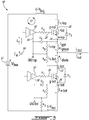
- FIG 4 is a schematic representation of a typical topology for an IGBT module.
- Figure 5 is a top plan view of an actual IGBT module having the topology of Figure 4 , the IGBT module including a circuit card and a casing.
- a conventional IGBT module 100 includes a first set of parallelized IGBT 102 defining the top IGBT Q 2 of Figure 3 and their associated diodes 104, a second set of parallelized IGBT 106 defining the bottom IGBT Q 1 and their associated diodes 108, a + Vbus tab 110, a -Vbus tab 112 and a load tab 114.
- IGBT module 100 Elements of the IGBT module 100 are mounted on a direct bonded copper (DBC) substrate 101. Because of the constraints on packaging of IGBT modules, the upper and lower IGBTs and diodes are often packaged in close proximity of each other, as shown on Figures 4 and 5 .
- DBC direct bonded copper
- FIG. 4 and 5 In the example of Figures 4 and 5 , four (4) IGBTs 102 are placed in parallel to form the top IGBT Q 2 while four (4) more IGBTS 106 are placed in parallel to form the bottom IGBT Q 1 of Figure 3 .
- the top freewheel diode D 2 and the bottom freewheel diode D 1 are each realized as sets of four (4) parallelized diodes 104, 108.
- the IGBTs and diodes are connected to traces of the DBC substrate 101.
- the tabs 110, 112 and 114 are mounted on the DBC substrate 101, itself mounted in a casing 103.
- collectors 22 of the various IGBTs are not visible since they are mounted directly on DBC traces, including a c-top trace 116 and a c-bot trace 122.
- Emitters 24 are connected via wires 120 to an e-top trace 117 and to an e-bot trace 118 while gates 26 are connected to g-top and g-bot traces via wires 121.
- cathodes of the various diodes are not visible, being directly mounted on the c-top 116 and c-bot 122 traces.
- Anodes of the various diodes are connected via wires 120 to the e-top 1 17 and to e-bot 118 traces.
- interconnections made via DBC traces, wire bonds 120, 121 and external connections create the parasitic inductances introduced in the foregoing description of Figure 3 .
- the e-bot trace 118 that forms a connection between the emitter 24 of the bottom IGBT Q 1 (IGBTs 106) and the external connection of -Vbus tab 112 contains a zigzag pattern that creates a fairly large parasitic inductance between these elements. Accordingly, a level of voltage across the emitter inductance L e-bot of the bottom IGBT Q 1 can be injected in the gate driver 26 of the bottom IGBT Q 1 using the compensation circuit of Figure 3 to create a negative voltage at its emitter 24, adequately slowing down the negative slope of the gate voltage.
- the wire bonds 120 interconnecting the emitter of the top IGBT Q 2 (IGBTs 102) to the c-bot trace 122 of the bottom IGBT Q 1 (IGBTs 106) are quite short. Therefore, the inductance between the emitter of the top IGBT Q 2 and the collector of the bottom IGBT Q 1 is quite small, in the order of a few nano-Henrys (nH).
- a level of voltage across the emitter inductance L e-top of the top IGBT Q 2 that can be injected in the gate driver 26 of the top IGBT Q 2 using the compensation circuit of Figure 3 to create a negative voltage at its emitter 24 of the top IGBT Q 2 to slow down the negative slope of the gate voltage may be too small to adequately limit the overvoltage of the top IGBT Q 2 .
- the comparatively small value of the upper emitter inductance L e - top may impact the effectiveness of the solution described hereinabove when applied without additional modification to the top IGBT Q 2 .
- the present disclosure also introduces a power converter, comprising the above-described topology and top and bottom power electronic switches.
- the power converter also includes a top gate driver having a reference electrically connected to the top power electronic switch emitter voltage sampling point and to the bottom power electronic switch collector voltage sampling point, as well as a bottom gate driver having a reference electrically connected to the bottom power electronic switch emitter voltage sampling point and to the negative voltage power supply tab sampling point
- Various aspects of the present disclosure generally address one or more of the problems of overvoltage present in power converters at the time of switching.
- Circuits operable to limit overvoltage in commutation cells, especially at turn-off of IGBTs, are described in international patent publications no WO 2013/082705 A1 , WO 2014/043795 and WO 2014/161080 A1 , WO 2015/070344 A1 , WO 2015/061901 A1 , WO 2015/070347 A1 and WO 2015/139132 A1 , all of which are authored by Jean-Marc Cyr et al.
- the present technology provides control of overvoltage and switching losses at turn-off of a power electronic switch of a power module. Circuits and methods presented herein are generally compatible with other solutions to limit overvoltage at turn-off of power electronic switches.
- di / dt at turn-off of a power electronic switch generates a voltage across stray inductances of the high frequency loop of the power module. This voltage is applied across the power electronic switch in addition to a bus voltage providing power to the power module.
- a solution based on the injection of a sample of the overvoltage present across the power electronic switch to a gate driver of the power electronic switch has been proposed. In the case of a pair of power electronic switches connected in series, this solution efficiently controls the overvoltage on a "bottom" power electronic switch.
- An improvement comprises defining a new physical topology for mounting power electronic switches, the topology providing a changed definition of parasitic inductances voltage and sampling points for voltages thereacross.
- parasitic inductance is used herein and in the appended claims to refer to the inductance created by the connections between the various components of an actual commutation cell.
- the voltage generated across some of the parasitic inductances is sampled and used to improve the operation of the commutation cell. Nevertheless, for clarity purpose, these inductances are referred to as parasitic inductances herein.
- IGBT isolated gate bipolar transistors
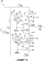
- FIG. 6 is a top plan view of an IGBT module according to an embodiment, the IGBT module including a circuit card and a casing.
- Figure 7 is a perspective view of the IGBT module of Figure 6 .
- Figure 8 is a perspective view of the IGBT module of Figure 6 , showing the circuit card and connectors, without the casing.
- a physical topology 200 is implemented in the form of a card, for example a direct bonded copper (DBC) substrate that can be mounted in a casing 202.
- the topology 200 is adapted for receiving a top power electronic switch, that optionally include a plurality of parallelized top IGBTs 204, and a bottom power electronic switch, that optionally include a plurality of parallelized bottom IGBTs 206.
- each IGBT includes a collector, a gate and an emitter.
- the topology 200 comprises a top collector trace 208, connected to a positive voltage power supply tab 210.
- the top collector trace 208 provides a connection area for the collectors of the top IGBTs 204.
- the topology 200 also comprises a bottom emitter trace 212 connected to a negative voltage power supply tab 214.
- the bottom emitter trace 212 provides a connection area for the emitters of the bottom IGBTs 206.
- a middle trace 216 is also included in the topology 200 that is a middle trace 216 connected to a load tab 218 that may be a phase tab in the case of a multiphase embodiment.
- the middle trace 216 has a connection area for the emitters of the top IGBTs 204 and a connection area for the collectors of the bottom IGBTs 206.
- Collectors of the top IGBTs 204 are in direct contact with the top collector trace 208 while collectors of the bottom IGBTs 206 are in direct contact with the middle trace 216.
- Wires 220 connect the emitters of the top IBGTs 204 to the middle trace 216 and wires 221 connect emitters of the bottom IGBTs 206 to the bottom emitter trace 212.
- Top freewheel diodes 222 are mounted in parallel to the top IGBTs 204 on the top collector trace 208 and bottom freewheel diodes 224 are mounted in parallel to the bottom IGBTs 206 on the middle trace 216.
- Traces are made of a conductive material, using for example direct bound copper (DBC).
- the topology 200 includes four (4) voltage-sampling points. These comprise a top IGBT emitter voltage sampling point 226 located on the middle trace 216 within the connection area for the emitters of the top IGBTs 204, a bottom IGBT collector voltage sampling point located 228 within a connection area of the middle trace 216 to the load tab 218, a bottom IGBT emitter voltage sampling point 230 located on the bottom emitter trace 212 within the connection area for the emitters of the IGBT 206, and a negative voltage power supply tab sampling point 232 located within a connection area of the bottom emitter trace 212 to the negative voltage power supply tab 214.
- the sampling points 226, 228, 230 and 232 are respectively connected to pins 234, 236, 238 and 240 that extend from a plane of the card supporting the topology 200 to provide connections to gate drivers (on a later Figure) located on a separate circuit card (not shown). It may be noted that the pins 234 and 238 directly connect, for example by welding, to the sampling points 226 and 230, respectively. On the other hand, the pins 236 and 240 are respectively welded on edges of the middle trace 216 and of the bottom emitter trace 212 and connect to the sampling points 228 and 232 via portions of the middle trace 216 and of the bottom emitter trace 212.
- Grooves 242 and 244 are provided to isolate strong currents flowing between the bottom IGBTs 206 and the tabs 218 and 214 so that the voltages on the pins 236 and 242 effectively reflect the voltages at the tabs 218 and 214, respectively.
- the top collector trace 208 forms a top collector inductance ( L c-top ), generally defined between the connection area for the positive voltage power supply tab 210 and points where the various top IGBTs 204 are mounted on the top collector trace.
- the bottom emitter trace 212 forms a bottom emitter inductance ( L e-bot ), generally between the connection area of the emitters of the bottom IGBTs 206, substantially at the bottom IGBT emitter voltage sampling point 230, and the connection area for the negative voltage power supply tab 214.
- the middle trace 216 forms a top emitter inductance ( L e-top ), generally between the connection area for the emitters of the top IGBTs 204, substantially at the top IGBT emitter voltage sampling point 226, and the connection area for the load tab 218.
- the middle trace 216 also forms a bottom collector inductance ( L c-bot ), generally between the connection area for the load tab 218 and points where the various bottom IGBTs 206 are mounted on the middle trace 216.
- the top emitter inductance ( L e-top ) and the bottom emitter inductance ( L e-bot ) may both be greater than the top collector inductance ( L c-top ).
- the disclosed topology when compared to earlier layouts, provides a reduction of the collector inductance values as well as an increase of the top emitter inductance value.
- An overall inductance in the high frequency loop of an IGBT leg built using the disclosed topology may, in some embodiments, remain similar to the overall inductance provided in earlier layouts, for example in the layout of Figures 4 and 5 , so that, resulting switching losses and switching speeds are not significantly impacted.
- the top emitter inductance is increased, it becomes much easier to configure the application of a voltage, sampled thereacross, to the gate driver of the top power electronic switch.
- emitters of the top IGBTs 204 and the bottom IGBTs 206 are respectively connected to the middle trace 216 and to the bottom emitter trace 212, via wires 220, over fairly broad connection areas.
- the middle trace 216 includes a groove 246 leading from the top IGBT emitter voltage sampling point 226 in a direction toward the load tab 218 while the bottom emitter trace 212 includes a groove 248 leading from the bottom IGBT emitter voltage sampling point 230 in a direction toward the negative voltage power supply tab 214.
- Currents from the IGBT 204 and 206 emitters are driven toward the sampling points 226 and 230 before flowing further to the tabs 218 and 214.
- Figures 6 , 7 and 8 also show a top gate trace 250 configured for connection to the gate of the top IGBTs 204 via wires 223 and a bottom gate trace 252 configured for connection to the gate of the IGBTs 206, via wires 225.
- Pins 254 and 256 that extend from the plane of the card supporting the topology 200 provide connections to respective top and bottom gate driver outputs (shown on a next Figure).
- the topology 200 can be used as a part of a power converter.
- Figure 9 is a circuit diagram of an IGBT leg configured to be used with the IGBT module of Figure 6 .
- An IGBT leg 300 is schematically illustrated. Some of its elements are mounted on the physical topology 200 of Figures 6 , 7 and 8 and some other elements of the IGBT leg 300 are mounted on a separate circuit card (not shown) that may for example be mounted atop the casing 202 that encloses the topology 200.
- the IGBT leg 300 includes the top IGBTs 204, the top freewheel diodes 222, the bottom IGBTs 206 and the bottom freewheel diodes 224, each of which is mounted on the topology 200 and may include a single device or a plurality of parallelized devices.
- the inductances L c-top , L e-top , L c-bot, and L e-bot are defined by the traces 208, 212 and 216 of the topology 200, as expressed hereinabove.
- the inductances L + Vbus , L -Vbus and L phase are defined by the positive voltage power supply tab 210, the negative voltage power supply tab 214 and the load tab 218 (also called phase tab in the case of a multiphase embodiment), respectively.
- the pins 234, 236, 238 and 240 that extend from the plane of the card supporting the topology 200 are connected on the IGBT leg 300 at the points shown on Figure 9 .
- a voltage across the top emitter inductance L e-top and the bottom collector inductance L c-bot is present between pins 234 and 236 and a voltage across the bottom emitter inductance L e-bot is present between pins 238 and 240.
- a top gate driver 302 is fed by a positive voltage supply +Vcc and by a negative voltage supply - V dd and has a reference 304.
- a control signal is fed at an input 303 of the top gate driver 302 to cause an output 305 to reach either of the + V cc above or -V dd below the reference 304, forming signals applied to the gate 26 of the top IGBT 204 via a gate resistor R 4 .
- the reference 304 of the top gate driver 302 is connected across gate-emitter in series with the emitter inductance of the top IGBT 204 via a compensation circuit that includes resistors and an optional turn-on diode.
- the reference 304 is electrically connected to the top IGBT emitter voltage sampling point 226, either directly via the pin 234 or, optionally, via a turn-on diode D 4 in series with a resistor R D4 and via the pin 234. If present, the turn-on diode D 4 is polarized to become short when an emitter voltage of the top IGBT 204 is higher than a voltage of the reference 304.
- the reference 304 is also electrically connected to the bottom IGBT collector voltage sampling point 228 via a resistor R 8 and via the pin 236.
- a resistor R 7 is optionally placed in parallel with the series combination of the turn-on diode D 4 with the resistor R D4 .
- the compensation circuit operates similarly during turn-on and turn-off of the top IGBT 204. If the turn-on diode D 4 is present and if the resistor R D4 is replaced by a short circuit, there is no compensation at turn-on. In the presence of the turn-on diode D 4 , selection of a proper value for the resistor R D4 allows to fine tune the turn-on of the top IGBT 204 independently from its turn-off, the compensation circuit forming a resistive divider between R D4 in parallel with R 7 , this parallel combination being in series with R 8 . It is to be noted that resistor R 7 may have an infinite value. Resistor R 7 is used to fine-tune the circuit, if necessary.
- a bottom gate driver 308 is also fed by a positive voltage supply + V cc and by a negative voltage supply -V dd and has a reference 310.
- a control signal is fed at an input 309 of the bottom gate driver 308 to cause an output 311 to reach either of the + V cc above or -V dd below the reference 310, forming signals applied to the gate 26 of the bottom IGBT 206 via a gate resistor R 1 .
- the reference 310 of the bottom gate driver 308 is connected across the emitter inductance of the bottom IGBT 206 via a compensation circuit including resistors and an optional turn-on diode.
- the bottom gate driver 308 is connected to the bottom IGBT 206 via a compensation circuit including resistors and an optional turn-on diode.
- the reference 310 is electrically connected to the bottom IGBT emitter voltage sampling point 230, either directly via the pin 238 or, optionally, via a turn-on diode D 3 in series with a resistor R D3 and via the pin 238. If present, the turn-on diode D 3 is polarized to become short when an emitter voltage of the bottom IGBT 206 is higher than a voltage of the reference 310.
- the reference 310 is also electrically connected to the negative voltage power supply tab sampling point 232 via a resistor R 10 and via the pin 240.
- a resistor R 9 is optionally placed in parallel with the turn-on diode D 3 in series with the resistor R D3 . If the turn-on diode D 3 is absent (or equivalently if the resistor R D3 has an infinite value), the compensation circuit operates similarly during turn-on and turn-off of the bottom IGBT 206. If the turn-on diode D 3 is present and if the resistor R D3 is replaced by a short circuit, there is no compensation at turn-on.
- resistor R D3 In the presence of the turn-on diode D 3 , selection of a proper value for the resistor R D3 allows to fine tune the turn-on of the bottom IGBT 206 independently from its turn-off, the compensation circuit forming a resistive divider between R D3 in parallel with R 9 , this parallel combination being in series with R 10 . It is to be noted that resistor R 9 may have an infinite value.
- a commutation cell formed of the top IGBT 204, its top gate driver 302 and the compensation circuit including the optional turn-on diode D 4 and the resistors R 7 and R 8 .
- the output 305 of the top gate driver 302 being at + V cc above the reference 304, it is essentially shorted and its emitter voltage present at the pin 234 is essentially equal to the + V bus voltage. This voltage equal to a voltage at the reference 304 and the turn-on diode D 4 is shorted.
- the output 305 When the input 303 provides a turn-off command to the gate driver 302, without the compensation circuit, the output 305 would quickly fall to -V dd and the top IGBT 204 would rapidly become an open circuit. The rapid reduction of current flowing therethrough would cause an excessive voltage across the L e-top , with the polarity as shown on Figure 9 , causing overvoltage.
- the compensation circuit and the present topology With the compensation circuit and the present topology, the emitter voltage at the pin 234 reduces below the voltage of the reference 304 and the turn-on diode D 4 becomes an open circuit. The voltage across the L e-top , between the pins 234 and 236 is divided between the resistors R 7 and R 8 , providing a sample of the overvoltage applied at the reference 304.
- a commutation cell formed of the bottom IGBT 206, its gate drive 208 and a compensation circuit including the turn-on diode D 3 , if present, and the resistors R 9 and R 10 operate in the same manner.
- topology for a power converter is illustrative only and are not intended to be in any way limiting. Other embodiments will readily suggest themselves to such persons with ordinary skill in the art having the benefit of the present disclosure. Furthermore, the topology may be customized to offer valuable solutions to existing needs and problems of overvoltage occurring in power electronic switches.
Landscapes
- Engineering & Computer Science (AREA)
- Power Engineering (AREA)
- Microelectronics & Electronic Packaging (AREA)
- Computer Hardware Design (AREA)
- Physics & Mathematics (AREA)
- Condensed Matter Physics & Semiconductors (AREA)
- General Physics & Mathematics (AREA)
- Chemical & Material Sciences (AREA)
- Materials Engineering (AREA)
- Geometry (AREA)
- Ceramic Engineering (AREA)
- Power Conversion In General (AREA)
- Inverter Devices (AREA)
- Electronic Switches (AREA)
Claims (16)
- Physikalische Topologie (200) zum Aufnehmen oberer und unterer Leistungselektronikschalter, wobei jeder Leistungselektronikschalter einen Kollektor, ein Gate und einen Emitter aufweist, wobei die Topologie umfasst:eine obere Kollektorbahn (208) und eine damit verbundene Positivspannungsversorgungslasche (210), wobei die obere Kollektorbahn einen Verbindungsbereich für den Kollektor des oberen Leistungselektronikschalters aufweist;eine untere Emitterbahn (212) und eine damit verbundene Negativspannungsversorgungslasche (214),wobei die untere Emitterbahn einen Verbindungsbereich für den Emitter des unteren Leistungselektronikschalters aufweist;eine mittlere Bahn (216) und eine damit verbundene Lastlasche (218),wobei die mittlere Bahn einen Verbindungsbereich für den Emitter des oberen Leistungselektronikschalters und einen Verbindungsbereich für den Kollektor des unteren Leistungselektronikschalters aufweist, wobei die mittlere Bahn eine obere Emitterinduktivität zwischen dem Verbindungsbereich für den Emitter des oberen Leistungselektronikschalters und der Lastlasche ausbildet, wobei die mittlere Leiterbahn auch eine untere Kollektorinduktivität zwischen der Lastlasche und dem Verbindungsbereich für den Kollektor des unteren Leistungselektronikschalters ausbildet;einen Emitterspannungsabtastpunkt (226) des oberen Leistungselektronikschalters, der sich auf der mittleren Bahn innerhalb des Verbindungsbereichs für den Emitter des oberen Leistungselektronikschalters befindet;einen Kollektorspannungsabtastpunkt (228) des unteren Leistungselektronikschalters, der sich innerhalb eines Verbindungsbereichs der mittleren Bahn zur Lastlasche befindet;einen Emitterspannungsabtastpunkt (230) des unteren Leistungselektronikschalters, der sich auf der unteren Emitterbahn innerhalb des Verbindungsbereichs für den Emitter des unteren Leistungselektronikschalters befindet;dadurch gekennzeichnet, dassdie mittlere Bahn (216) unitär und kontinuierlich ist; unddie Topologie ferner umfasst:
einen Abtastpunkt (232) der Negativspannungsversorgungslasche, der sich innerhalb eines Verbindungsbereichs der unteren Emitterbahn zur Negativspannungsversorgungslasche befindet. - Topologie nach Anspruch 1, wobei:die obere Kollektorbahn (208) eine Induktivität des oberen Kollektors ausbildet; unddie untere Emitterbahn (212) eine Induktivität des unteren Emitters ausbildet.
- Topologie nach Anspruch 2, wobei:die Induktivität des oberen Emitters größer als die Induktivität des oberen Kollektors und größer als die Induktivität des unteren Kollektors ist; unddie Induktivität des unteren Emitters größer als die Induktivität des oberen Kollektors und größer als die Induktivität des unteren Kollektors ist.
- Topologie nach einem der Ansprüche 1 bis 3, wobei:der Verbindungsbereich für den Kollektor des oberen Leistungselektronikschalters und der Verbindungsbereich für den Kollektor des unteren Leistungselektronikschalters für einen direkten Kontakt mit den Kollektoren der Leistungselektronikschalter konfiguriert sind; undder Verbindungsbereich für den Emitter des oberen Leistungselektronikschalters und der Verbindungsbereich für den Emitter des unteren Leistungselektronikschalters für eine Verbindung mit den Emittern der Leistungselektronikschalter über Drähte konfiguriert sind.
- Topologie nach einem der Ansprüche 1 bis 4, wobei:die obere Kollektorbahn (208) zum Montieren einer Diode parallel zu dem oberen Leistungselektronikschalter konfiguriert ist; unddie mittlere Bahn (216) zum Montieren einer Diode parallel zu dem unteren Leistungselektronikschalter konfiguriert ist.
- Topologie nach einem der Ansprüche 1 bis 5, wobei:die obere Kollektorbahn (208) zum Montieren einer Vielzahl parallelisierter oberer Leistungselektronikschalter konfiguriert ist; unddie mittlere Bahn (216) zum Montieren einer Vielzahl parallelisierter unterer Leistungselektronikschalter konfiguriert ist.
- Topologie nach Anspruch 6, wobei:die mittlere Bahn (216) eine Nut beinhaltet, die von dem Emitterspannungsabtastpunkt (226) des oberen Leistungselektronikschalters in eine Richtung zu der Lastlasche (218) führt, um Ströme in jedem der parallelisierten oberen Leistungselektronikschalter im Wesentlichen auszugleichen; unddie untere Emitterbahn (212) eine Nut beinhaltet, die von dem Emitterspannungsabtastpunkt (230) des unteren Leistungselektronikschalters in eine Richtung zu der Negativspannungsversorgungslasche führt, um Ströme in jedem der parallelisierten unteren Leistungselektronikschalter im Wesentlichen auszugleichen.
- Topologie nach einem der Ansprüche 1 bis 7, wobei die Topologie ein Direct-Bonded-Copper-Substrat, DBC-Substrat, umfasst, und die obere Kollektorbahn (208), die untere Emitterbahn (212) und die mittlere Bahn (216) auf dem DBC-Substrat sind.
- Topologie nach Anspruch 8, wobei jeder von dem Emitterspannungsabtastpunkt (226) des oberen Leistungselektronikschalters, dem Kollektorspannungsabtastpunkt (228) des unteren Leistungselektronikschalters, dem Emitterspannungsabtastpunkt (230) des unteren Leistungselektronikschalters und dem Abtastpunkt (232) der Negativspannungsversorgungslasche elektrisch verbindbar mit einer entsprechenden Gate-Treiber-Verbindung ist, die sich von einer Ebene des DBC-Substrats erstreckt und für eine Verbindung zu einer separaten Schaltkarte ausgelegt ist.
- Topologie nach den Ansprüchen 1 bis 8, umfassend:eine obere Gate-Bahn (250), ausgelegt für eine Verbindung zum Gate des oberen Leistungselektronikschalters über einen oder mehrere Drähte (223); undeine untere Gate-Bahn (252), ausgelegt für eine Verbindung zum Gate des unteren Leistungselektronikschalters über einen oder mehrere Drähte (225).
- Topologie nach Anspruch 10, umfassend ein Paar von Gate-Treiber-Verbindungen, die sich von der oberen bzw. unteren Gate-Bahn (250, 252) erstrecken und für eine Verbindung zu entsprechenden oberen und unteren Gate-Treiber-Ausgängen konfiguriert sind.
- Topologie nach einem der Ansprüche 1 bis 11, wobei die Lastlasche (218) eine Phasenlasche ist.
- Topologie nach einem der Ansprüche 1 bis 12, wobei der obere und untere Leistungselektronikschalter Bipolartransistoren mit isolierter Gate-Elektrode (IGBT) enthalten.
- Leistungswandler, umfassend:die Topologie (200) und den oberen und unteren Leistungselektronikschalter nach einem der Ansprüche 1 bis 13;einen oberen Gate-Treiber (302) mit einer Referenz (304), elektrisch verbunden mit dem Emitterspannungsabtastpunkt (226) des oberen Leistungselektronikschalters und dem Kollektorspannungsabtastpunkt (228) des unteren Leistungselektronikschalters; undeinen unteren Gate-Treiber (308) mit einer Referenz (310), elektrisch verbunden mit dem Emitterspannungsabtastpunkt (230) des unteren Leistungselektronikschalters und dem Abtastpunkt (232) der Negativspannungsversorgungslasche.
- Leistungswandler nach Anspruch 14, wobei:der Leistungswandler eine erste Einschaltdiode, einen ersten Widerstand, einen zweiten Widerstand, eine zweite Einschaltdiode, einen dritten Widerstand und einen vierten Widerstand umfasst;die Referenz (304) des oberen Gate-Treibers (302) über die erste Einschaltdiode parallel zu dem ersten Widerstand verbunden ist mit dem Emitterspannungsabtastpunkt (226) des oberen Leistungselektronikschalters, wobei die erste Einschaltdiode polarisiert ist, um den ersten Widerstand kurzzuschließen, wenn eine Spannung des oberen Leistungselektronikschalteremitters höher ist als eine Spannung der Referenz des oberen Gate-Treibers;die Referenz (304) des oberen Gate-Treibers (302) über den zweiten Widerstand verbunden ist mit dem Kollektorspannungsabtastpunkt (228) des unteren Leistungselektronikschalters;die Referenz (310) des unteren Gate-Treibers (308) über die zweite Einschaltdiode parallel zu dem dritten Widerstand verbunden ist mit dem Emitterspannungsabtastpunkt (230) des unteren Leistungselektronikschalters, wobei die zweite Einschaltdiode polarisiert ist, um den dritten Widerstand kurzzuschließen, wenn eine Spannung des unteren Leistungselektronikschalteremitters höher ist als eine Spannung der Referenz des unteren Gate-Treibers;die Referenz (310) des unteren Gate-Treibers (308) über den vierten Widerstand verbunden ist mit dem Abtastpunkt (232) der Negativspannungsversorgungslasche.
- Dreiphasenleistungswandler, umfassend drei Leistungswandler nach einem der Ansprüche 14 oder 15.
Applications Claiming Priority (2)
| Application Number | Priority Date | Filing Date | Title |
|---|---|---|---|
| US201562183437P | 2015-06-23 | 2015-06-23 | |
| PCT/CA2016/050702 WO2016205929A1 (en) | 2015-06-23 | 2016-06-16 | Physical topology for a power converter |
Publications (3)
| Publication Number | Publication Date |
|---|---|
| EP3314656A1 EP3314656A1 (de) | 2018-05-02 |
| EP3314656A4 EP3314656A4 (de) | 2019-02-20 |
| EP3314656B1 true EP3314656B1 (de) | 2021-08-04 |
Family
ID=57584333
Family Applications (1)
| Application Number | Title | Priority Date | Filing Date |
|---|---|---|---|
| EP16813424.5A Active EP3314656B1 (de) | 2015-06-23 | 2016-06-16 | Physikalische topologie für einen leistungswandler |
Country Status (8)
| Country | Link |
|---|---|
| US (1) | US10277112B2 (de) |
| EP (1) | EP3314656B1 (de) |
| JP (1) | JP2018520625A (de) |
| KR (1) | KR20180019610A (de) |
| CN (1) | CN107851661B (de) |
| CA (1) | CA2989672C (de) |
| HK (1) | HK1252919A1 (de) |
| WO (1) | WO2016205929A1 (de) |
Families Citing this family (12)
| Publication number | Priority date | Publication date | Assignee | Title |
|---|---|---|---|---|
| WO2017045071A1 (en) * | 2015-09-14 | 2017-03-23 | Tm4 Inc. | Power converter configured for limiting switching overvoltage |
| JP7210446B2 (ja) * | 2016-11-25 | 2023-01-23 | ヒタチ・エナジー・スウィツァーランド・アクチェンゲゼルシャフト | パワー半導体モジュール |
| JP7163054B2 (ja) * | 2017-04-20 | 2022-10-31 | ローム株式会社 | 半導体装置 |
| US11233037B2 (en) | 2017-04-20 | 2022-01-25 | Rohm Co., Ltd. | Semiconductor device |
| CN107946293A (zh) * | 2017-12-22 | 2018-04-20 | 江苏宏微科技股份有限公司 | 一种功率模块封装结构 |
| US10418307B2 (en) * | 2017-12-22 | 2019-09-17 | Deere & Company | Electronic assembly with a direct bonded copper substrate |
| KR102596436B1 (ko) | 2018-02-20 | 2023-11-01 | 삼성전자주식회사 | 사용자 발화를 처리하는 시스템 및 그 시스템의 제어 방법 |
| EP3806313A4 (de) * | 2018-05-28 | 2021-07-21 | Mitsubishi Electric Corporation | Stromumwandlungsvorrichtung |
| CN108447846A (zh) * | 2018-06-06 | 2018-08-24 | 臻驱科技(上海)有限公司 | 一种功率半导体模块衬底及功率半导体模块 |
| CN108447847A (zh) * | 2018-06-06 | 2018-08-24 | 臻驱科技(上海)有限公司 | 一种功率半导体模块衬底及功率半导体模块 |
| EP3879685A4 (de) * | 2018-11-05 | 2021-12-01 | Mitsubishi Electric Corporation | Gate-treiberschaltung und leistungsumwandlungsvorrichtung |
| JP7491043B2 (ja) | 2020-05-13 | 2024-05-28 | 富士電機株式会社 | 半導体モジュール |
Family Cites Families (12)
| Publication number | Priority date | Publication date | Assignee | Title |
|---|---|---|---|---|
| EP0954899A2 (de) | 1997-01-24 | 1999-11-10 | Fische, LLC | Hocheffizienter stromrichter |
| JP3454186B2 (ja) * | 1999-05-14 | 2003-10-06 | 株式会社日立製作所 | 電力変換装置 |
| JP4432953B2 (ja) | 2006-09-27 | 2010-03-17 | 株式会社日立製作所 | 半導体電力変換装置 |
| IN2014DN03024A (de) | 2011-12-07 | 2015-05-08 | Tm4 Inc | |
| US9812987B2 (en) * | 2012-09-24 | 2017-11-07 | Tm4 Inc. | Topology for controlled power switch module |
| EP2982038B1 (de) | 2013-04-04 | 2019-06-19 | TM4 Inc. | Kommutierungszelle und kompensationsschaltung dafür |
| CN103296905B (zh) * | 2013-05-24 | 2015-07-29 | 西安理工大学 | 三相电压型功率因数校正变换器的自适应控制方法 |
| KR20160079807A (ko) | 2013-11-01 | 2016-07-06 | 티엠4 인코포레이티드 | 스위칭 과전압을 제한하는 구성의 전력 변환기 |
| CN105814781B (zh) | 2013-11-14 | 2018-10-12 | Tm4股份有限公司 | 换向单元、电力变换器和具有动态控制的电压增益的补偿电路 |
| CA2930188A1 (en) * | 2013-11-14 | 2015-05-21 | Tm4 Inc. | Compensation circuit, commutation cell and power converter controlling turn-on and turn-off of a power electronic switch |
| JP2017511115A (ja) | 2014-03-20 | 2017-04-13 | ティーエム4・インコーポレーテッド | 電子スイッチのコレクタ−エミッタ間電圧の変動を制御するゲートドライバおよび同ゲートドライバを含む回路 |
| US9595954B2 (en) * | 2014-11-10 | 2017-03-14 | Nxp Usa, Inc. | Method and circuit for recharging a bootstrap capacitor using a transfer capacitor |
-
2016
- 2016-06-16 EP EP16813424.5A patent/EP3314656B1/de active Active
- 2016-06-16 CA CA2989672A patent/CA2989672C/en active Active
- 2016-06-16 US US15/738,314 patent/US10277112B2/en active Active
- 2016-06-16 JP JP2017566727A patent/JP2018520625A/ja not_active Abandoned
- 2016-06-16 KR KR1020177037385A patent/KR20180019610A/ko unknown
- 2016-06-16 WO PCT/CA2016/050702 patent/WO2016205929A1/en active Application Filing
- 2016-06-16 CN CN201680043194.0A patent/CN107851661B/zh active Active
-
2018
- 2018-09-24 HK HK18112271.5A patent/HK1252919A1/zh unknown
Also Published As
| Publication number | Publication date |
|---|---|
| HK1252919A1 (zh) | 2019-06-06 |
| CN107851661B (zh) | 2021-09-07 |
| CA2989672A1 (en) | 2016-12-29 |
| EP3314656A1 (de) | 2018-05-02 |
| US20180183321A1 (en) | 2018-06-28 |
| WO2016205929A1 (en) | 2016-12-29 |
| CA2989672C (en) | 2022-11-29 |
| EP3314656A4 (de) | 2019-02-20 |
| CN107851661A (zh) | 2018-03-27 |
| US10277112B2 (en) | 2019-04-30 |
| KR20180019610A (ko) | 2018-02-26 |
| JP2018520625A (ja) | 2018-07-26 |
Similar Documents
| Publication | Publication Date | Title |
|---|---|---|
| EP3314656B1 (de) | Physikalische topologie für einen leistungswandler | |
| US9882465B2 (en) | Commutation cell, power converter and compensation circuit having dynamically controlled voltage gains | |
| US8916882B2 (en) | Switching circuit and semiconductor module | |
| CN105308864B (zh) | 整流单元及其补偿电路 | |
| US9774244B2 (en) | Power converter configured for limiting switching overvoltage | |
| US9768693B2 (en) | Compensation circuit, commutation cell and power converter controlling turn-on and turn-off of a power electronic switch | |
| US10615787B2 (en) | Switch drive circuit for switch reducing LC resonance | |
| EP2789092B1 (de) | Abschaltbare überspannungssbegrenzung für igbt | |
| CN104756390B (zh) | 用于受控电源开关模块的拓扑 | |
| JP5619673B2 (ja) | スイッチング回路及び半導体モジュール | |
| US10468971B2 (en) | Power converter configured for limiting switching overvoltage |
Legal Events
| Date | Code | Title | Description |
|---|---|---|---|
| STAA | Information on the status of an ep patent application or granted ep patent |
Free format text: STATUS: THE INTERNATIONAL PUBLICATION HAS BEEN MADE |
|
| PUAI | Public reference made under article 153(3) epc to a published international application that has entered the european phase |
Free format text: ORIGINAL CODE: 0009012 |
|
| STAA | Information on the status of an ep patent application or granted ep patent |
Free format text: STATUS: REQUEST FOR EXAMINATION WAS MADE |
|
| 17P | Request for examination filed |
Effective date: 20180117 |
|
| AK | Designated contracting states |
Kind code of ref document: A1 Designated state(s): AL AT BE BG CH CY CZ DE DK EE ES FI FR GB GR HR HU IE IS IT LI LT LU LV MC MK MT NL NO PL PT RO RS SE SI SK SM TR |
|
| AX | Request for extension of the european patent |
Extension state: BA ME |
|
| DAV | Request for validation of the european patent (deleted) | ||
| DAX | Request for extension of the european patent (deleted) | ||
| A4 | Supplementary search report drawn up and despatched |
Effective date: 20190122 |
|
| RIC1 | Information provided on ipc code assigned before grant |
Ipc: H02M 7/538 20070101ALI20190117BHEP Ipc: H02M 3/155 20060101ALI20190117BHEP Ipc: H02M 1/08 20060101ALI20190117BHEP Ipc: H02M 1/32 20070101ALI20190117BHEP Ipc: H02M 7/00 20060101ALI20190117BHEP Ipc: H02M 1/00 20060101AFI20190117BHEP |
|
| RAP1 | Party data changed (applicant data changed or rights of an application transferred) |
Owner name: DANA TM4 INC. |
|
| REG | Reference to a national code |
Ref country code: DE Ref legal event code: R079 Ref document number: 602016061704 Country of ref document: DE Free format text: PREVIOUS MAIN CLASS: H01L0029730000 Ipc: H02M0001000000 |
|
| RIC1 | Information provided on ipc code assigned before grant |
Ipc: H02M 7/538 20070101ALI20201211BHEP Ipc: H02M 1/08 20060101ALI20201211BHEP Ipc: H02M 3/155 20060101ALI20201211BHEP Ipc: H02M 1/00 20060101AFI20201211BHEP Ipc: H01L 23/48 20060101ALI20201211BHEP Ipc: H02M 7/00 20060101ALI20201211BHEP Ipc: H02M 1/32 20070101ALI20201211BHEP |
|
| GRAP | Despatch of communication of intention to grant a patent |
Free format text: ORIGINAL CODE: EPIDOSNIGR1 |
|
| STAA | Information on the status of an ep patent application or granted ep patent |
Free format text: STATUS: GRANT OF PATENT IS INTENDED |
|
| INTG | Intention to grant announced |
Effective date: 20210129 |
|
| GRAS | Grant fee paid |
Free format text: ORIGINAL CODE: EPIDOSNIGR3 |
|
| GRAA | (expected) grant |
Free format text: ORIGINAL CODE: 0009210 |
|
| STAA | Information on the status of an ep patent application or granted ep patent |
Free format text: STATUS: THE PATENT HAS BEEN GRANTED |
|
| AK | Designated contracting states |
Kind code of ref document: B1 Designated state(s): AL AT BE BG CH CY CZ DE DK EE ES FI FR GB GR HR HU IE IS IT LI LT LU LV MC MK MT NL NO PL PT RO RS SE SI SK SM TR |
|
| REG | Reference to a national code |
Ref country code: GB Ref legal event code: FG4D |
|
| REG | Reference to a national code |
Ref country code: AT Ref legal event code: REF Ref document number: 1418017 Country of ref document: AT Kind code of ref document: T Effective date: 20210815 |
|
| REG | Reference to a national code |
Ref country code: CH Ref legal event code: EP |
|
| REG | Reference to a national code |
Ref country code: DE Ref legal event code: R096 Ref document number: 602016061704 Country of ref document: DE |
|
| REG | Reference to a national code |
Ref country code: IE Ref legal event code: FG4D |
|
| REG | Reference to a national code |
Ref country code: LT Ref legal event code: MG9D |
|
| REG | Reference to a national code |
Ref country code: NL Ref legal event code: MP Effective date: 20210804 |
|
| REG | Reference to a national code |
Ref country code: AT Ref legal event code: MK05 Ref document number: 1418017 Country of ref document: AT Kind code of ref document: T Effective date: 20210804 |
|
| PG25 | Lapsed in a contracting state [announced via postgrant information from national office to epo] |
Ref country code: RS Free format text: LAPSE BECAUSE OF FAILURE TO SUBMIT A TRANSLATION OF THE DESCRIPTION OR TO PAY THE FEE WITHIN THE PRESCRIBED TIME-LIMIT Effective date: 20210804 Ref country code: SE Free format text: LAPSE BECAUSE OF FAILURE TO SUBMIT A TRANSLATION OF THE DESCRIPTION OR TO PAY THE FEE WITHIN THE PRESCRIBED TIME-LIMIT Effective date: 20210804 Ref country code: NO Free format text: LAPSE BECAUSE OF FAILURE TO SUBMIT A TRANSLATION OF THE DESCRIPTION OR TO PAY THE FEE WITHIN THE PRESCRIBED TIME-LIMIT Effective date: 20211104 Ref country code: PT Free format text: LAPSE BECAUSE OF FAILURE TO SUBMIT A TRANSLATION OF THE DESCRIPTION OR TO PAY THE FEE WITHIN THE PRESCRIBED TIME-LIMIT Effective date: 20211206 Ref country code: HR Free format text: LAPSE BECAUSE OF FAILURE TO SUBMIT A TRANSLATION OF THE DESCRIPTION OR TO PAY THE FEE WITHIN THE PRESCRIBED TIME-LIMIT Effective date: 20210804 Ref country code: FI Free format text: LAPSE BECAUSE OF FAILURE TO SUBMIT A TRANSLATION OF THE DESCRIPTION OR TO PAY THE FEE WITHIN THE PRESCRIBED TIME-LIMIT Effective date: 20210804 Ref country code: ES Free format text: LAPSE BECAUSE OF FAILURE TO SUBMIT A TRANSLATION OF THE DESCRIPTION OR TO PAY THE FEE WITHIN THE PRESCRIBED TIME-LIMIT Effective date: 20210804 Ref country code: BG Free format text: LAPSE BECAUSE OF FAILURE TO SUBMIT A TRANSLATION OF THE DESCRIPTION OR TO PAY THE FEE WITHIN THE PRESCRIBED TIME-LIMIT Effective date: 20211104 Ref country code: AT Free format text: LAPSE BECAUSE OF FAILURE TO SUBMIT A TRANSLATION OF THE DESCRIPTION OR TO PAY THE FEE WITHIN THE PRESCRIBED TIME-LIMIT Effective date: 20210804 Ref country code: LT Free format text: LAPSE BECAUSE OF FAILURE TO SUBMIT A TRANSLATION OF THE DESCRIPTION OR TO PAY THE FEE WITHIN THE PRESCRIBED TIME-LIMIT Effective date: 20210804 |
|
| PG25 | Lapsed in a contracting state [announced via postgrant information from national office to epo] |
Ref country code: PL Free format text: LAPSE BECAUSE OF FAILURE TO SUBMIT A TRANSLATION OF THE DESCRIPTION OR TO PAY THE FEE WITHIN THE PRESCRIBED TIME-LIMIT Effective date: 20210804 Ref country code: LV Free format text: LAPSE BECAUSE OF FAILURE TO SUBMIT A TRANSLATION OF THE DESCRIPTION OR TO PAY THE FEE WITHIN THE PRESCRIBED TIME-LIMIT Effective date: 20210804 Ref country code: GR Free format text: LAPSE BECAUSE OF FAILURE TO SUBMIT A TRANSLATION OF THE DESCRIPTION OR TO PAY THE FEE WITHIN THE PRESCRIBED TIME-LIMIT Effective date: 20211105 |
|
| PG25 | Lapsed in a contracting state [announced via postgrant information from national office to epo] |
Ref country code: NL Free format text: LAPSE BECAUSE OF FAILURE TO SUBMIT A TRANSLATION OF THE DESCRIPTION OR TO PAY THE FEE WITHIN THE PRESCRIBED TIME-LIMIT Effective date: 20210804 |
|
| PG25 | Lapsed in a contracting state [announced via postgrant information from national office to epo] |
Ref country code: DK Free format text: LAPSE BECAUSE OF FAILURE TO SUBMIT A TRANSLATION OF THE DESCRIPTION OR TO PAY THE FEE WITHIN THE PRESCRIBED TIME-LIMIT Effective date: 20210804 |
|
| REG | Reference to a national code |
Ref country code: DE Ref legal event code: R097 Ref document number: 602016061704 Country of ref document: DE |
|
| PG25 | Lapsed in a contracting state [announced via postgrant information from national office to epo] |
Ref country code: SM Free format text: LAPSE BECAUSE OF FAILURE TO SUBMIT A TRANSLATION OF THE DESCRIPTION OR TO PAY THE FEE WITHIN THE PRESCRIBED TIME-LIMIT Effective date: 20210804 Ref country code: SK Free format text: LAPSE BECAUSE OF FAILURE TO SUBMIT A TRANSLATION OF THE DESCRIPTION OR TO PAY THE FEE WITHIN THE PRESCRIBED TIME-LIMIT Effective date: 20210804 Ref country code: RO Free format text: LAPSE BECAUSE OF FAILURE TO SUBMIT A TRANSLATION OF THE DESCRIPTION OR TO PAY THE FEE WITHIN THE PRESCRIBED TIME-LIMIT Effective date: 20210804 Ref country code: EE Free format text: LAPSE BECAUSE OF FAILURE TO SUBMIT A TRANSLATION OF THE DESCRIPTION OR TO PAY THE FEE WITHIN THE PRESCRIBED TIME-LIMIT Effective date: 20210804 Ref country code: CZ Free format text: LAPSE BECAUSE OF FAILURE TO SUBMIT A TRANSLATION OF THE DESCRIPTION OR TO PAY THE FEE WITHIN THE PRESCRIBED TIME-LIMIT Effective date: 20210804 Ref country code: AL Free format text: LAPSE BECAUSE OF FAILURE TO SUBMIT A TRANSLATION OF THE DESCRIPTION OR TO PAY THE FEE WITHIN THE PRESCRIBED TIME-LIMIT Effective date: 20210804 |
|
| PLBE | No opposition filed within time limit |
Free format text: ORIGINAL CODE: 0009261 |
|
| STAA | Information on the status of an ep patent application or granted ep patent |
Free format text: STATUS: NO OPPOSITION FILED WITHIN TIME LIMIT |
|
| 26N | No opposition filed |
Effective date: 20220506 |
|
| PG25 | Lapsed in a contracting state [announced via postgrant information from national office to epo] |
Ref country code: IT Free format text: LAPSE BECAUSE OF FAILURE TO SUBMIT A TRANSLATION OF THE DESCRIPTION OR TO PAY THE FEE WITHIN THE PRESCRIBED TIME-LIMIT Effective date: 20210804 |
|
| PG25 | Lapsed in a contracting state [announced via postgrant information from national office to epo] |
Ref country code: SI Free format text: LAPSE BECAUSE OF FAILURE TO SUBMIT A TRANSLATION OF THE DESCRIPTION OR TO PAY THE FEE WITHIN THE PRESCRIBED TIME-LIMIT Effective date: 20210804 |
|
| PG25 | Lapsed in a contracting state [announced via postgrant information from national office to epo] |
Ref country code: MC Free format text: LAPSE BECAUSE OF FAILURE TO SUBMIT A TRANSLATION OF THE DESCRIPTION OR TO PAY THE FEE WITHIN THE PRESCRIBED TIME-LIMIT Effective date: 20210804 |
|
| REG | Reference to a national code |
Ref country code: CH Ref legal event code: PL |
|
| REG | Reference to a national code |
Ref country code: BE Ref legal event code: MM Effective date: 20220630 |
|
| GBPC | Gb: european patent ceased through non-payment of renewal fee |
Effective date: 20220616 |
|
| PG25 | Lapsed in a contracting state [announced via postgrant information from national office to epo] |
Ref country code: LU Free format text: LAPSE BECAUSE OF NON-PAYMENT OF DUE FEES Effective date: 20220616 Ref country code: LI Free format text: LAPSE BECAUSE OF NON-PAYMENT OF DUE FEES Effective date: 20220630 Ref country code: IE Free format text: LAPSE BECAUSE OF NON-PAYMENT OF DUE FEES Effective date: 20220616 Ref country code: CH Free format text: LAPSE BECAUSE OF NON-PAYMENT OF DUE FEES Effective date: 20220630 Ref country code: FR Free format text: LAPSE BECAUSE OF NON-PAYMENT OF DUE FEES Effective date: 20220630 |
|
| PG25 | Lapsed in a contracting state [announced via postgrant information from national office to epo] |
Ref country code: GB Free format text: LAPSE BECAUSE OF NON-PAYMENT OF DUE FEES Effective date: 20220616 Ref country code: BE Free format text: LAPSE BECAUSE OF NON-PAYMENT OF DUE FEES Effective date: 20220630 |
|
| P01 | Opt-out of the competence of the unified patent court (upc) registered |
Effective date: 20230524 |
|
| PG25 | Lapsed in a contracting state [announced via postgrant information from national office to epo] |
Ref country code: HU Free format text: LAPSE BECAUSE OF FAILURE TO SUBMIT A TRANSLATION OF THE DESCRIPTION OR TO PAY THE FEE WITHIN THE PRESCRIBED TIME-LIMIT; INVALID AB INITIO Effective date: 20160616 |
|
| PG25 | Lapsed in a contracting state [announced via postgrant information from national office to epo] |
Ref country code: MK Free format text: LAPSE BECAUSE OF FAILURE TO SUBMIT A TRANSLATION OF THE DESCRIPTION OR TO PAY THE FEE WITHIN THE PRESCRIBED TIME-LIMIT Effective date: 20210804 Ref country code: CY Free format text: LAPSE BECAUSE OF FAILURE TO SUBMIT A TRANSLATION OF THE DESCRIPTION OR TO PAY THE FEE WITHIN THE PRESCRIBED TIME-LIMIT Effective date: 20210804 |
|
| PG25 | Lapsed in a contracting state [announced via postgrant information from national office to epo] |
Ref country code: TR Free format text: LAPSE BECAUSE OF FAILURE TO SUBMIT A TRANSLATION OF THE DESCRIPTION OR TO PAY THE FEE WITHIN THE PRESCRIBED TIME-LIMIT Effective date: 20210804 |
|
| PGFP | Annual fee paid to national office [announced via postgrant information from national office to epo] |
Ref country code: DE Payment date: 20240521 Year of fee payment: 9 |