EP3312596B1 - Verfahren und vorrichtung zur materialbahnbeobachtung und materialbahninspektion - Google Patents
Verfahren und vorrichtung zur materialbahnbeobachtung und materialbahninspektion Download PDFInfo
- Publication number
- EP3312596B1 EP3312596B1 EP17195965.3A EP17195965A EP3312596B1 EP 3312596 B1 EP3312596 B1 EP 3312596B1 EP 17195965 A EP17195965 A EP 17195965A EP 3312596 B1 EP3312596 B1 EP 3312596B1
- Authority
- EP
- European Patent Office
- Prior art keywords
- material web
- picture
- binning
- active area
- point
- Prior art date
- Legal status (The legal status is an assumption and is not a legal conclusion. Google has not performed a legal analysis and makes no representation as to the accuracy of the status listed.)
- Active
Links
- 239000000463 material Substances 0.000 title claims description 167
- 238000000034 method Methods 0.000 title claims description 64
- 238000007689 inspection Methods 0.000 title description 37
- 239000011159 matrix material Substances 0.000 claims description 123
- 230000006870 function Effects 0.000 claims description 83
- 238000012544 monitoring process Methods 0.000 claims description 23
- 230000004044 response Effects 0.000 claims description 4
- 230000007704 transition Effects 0.000 claims description 4
- 230000008569 process Effects 0.000 claims description 3
- 230000001419 dependent effect Effects 0.000 claims 1
- 230000007547 defect Effects 0.000 description 23
- 238000005286 illumination Methods 0.000 description 12
- 230000008901 benefit Effects 0.000 description 6
- 239000000047 product Substances 0.000 description 6
- 230000000007 visual effect Effects 0.000 description 6
- 230000003252 repetitive effect Effects 0.000 description 4
- 230000000717 retained effect Effects 0.000 description 4
- 230000001427 coherent effect Effects 0.000 description 3
- 230000003287 optical effect Effects 0.000 description 3
- 238000004806 packaging method and process Methods 0.000 description 3
- 230000009467 reduction Effects 0.000 description 3
- 230000009286 beneficial effect Effects 0.000 description 2
- 238000013461 design Methods 0.000 description 2
- 238000001514 detection method Methods 0.000 description 2
- 230000006866 deterioration Effects 0.000 description 2
- 238000011161 development Methods 0.000 description 2
- 238000012545 processing Methods 0.000 description 2
- 238000000275 quality assurance Methods 0.000 description 2
- 230000001960 triggered effect Effects 0.000 description 2
- PLXMOAALOJOTIY-FPTXNFDTSA-N Aesculin Natural products OC[C@@H]1[C@@H](O)[C@H](O)[C@@H](O)[C@H](O)[C@H]1Oc2cc3C=CC(=O)Oc3cc2O PLXMOAALOJOTIY-FPTXNFDTSA-N 0.000 description 1
- 206010034960 Photophobia Diseases 0.000 description 1
- 230000006978 adaptation Effects 0.000 description 1
- 230000005540 biological transmission Effects 0.000 description 1
- 239000000109 continuous material Substances 0.000 description 1
- 238000012937 correction Methods 0.000 description 1
- 238000001739 density measurement Methods 0.000 description 1
- 238000004090 dissolution Methods 0.000 description 1
- 238000009826 distribution Methods 0.000 description 1
- 230000000694 effects Effects 0.000 description 1
- 239000004744 fabric Substances 0.000 description 1
- 208000013469 light sensitivity Diseases 0.000 description 1
- 238000012423 maintenance Methods 0.000 description 1
- 238000004519 manufacturing process Methods 0.000 description 1
- 238000005259 measurement Methods 0.000 description 1
- 238000012806 monitoring device Methods 0.000 description 1
- 239000002994 raw material Substances 0.000 description 1
- 238000005096 rolling process Methods 0.000 description 1
- 230000003595 spectral effect Effects 0.000 description 1
- 238000012360 testing method Methods 0.000 description 1
Images


Classifications
-
- G—PHYSICS
- G01—MEASURING; TESTING
- G01N—INVESTIGATING OR ANALYSING MATERIALS BY DETERMINING THEIR CHEMICAL OR PHYSICAL PROPERTIES
- G01N21/00—Investigating or analysing materials by the use of optical means, i.e. using sub-millimetre waves, infrared, visible or ultraviolet light
- G01N21/84—Systems specially adapted for particular applications
- G01N21/88—Investigating the presence of flaws or contamination
- G01N21/89—Investigating the presence of flaws or contamination in moving material, e.g. running paper or textiles
- G01N21/8901—Optical details; Scanning details
-
- G—PHYSICS
- G06—COMPUTING; CALCULATING OR COUNTING
- G06T—IMAGE DATA PROCESSING OR GENERATION, IN GENERAL
- G06T7/00—Image analysis
- G06T7/0002—Inspection of images, e.g. flaw detection
- G06T7/0004—Industrial image inspection
-
- G—PHYSICS
- G01—MEASURING; TESTING
- G01N—INVESTIGATING OR ANALYSING MATERIALS BY DETERMINING THEIR CHEMICAL OR PHYSICAL PROPERTIES
- G01N21/00—Investigating or analysing materials by the use of optical means, i.e. using sub-millimetre waves, infrared, visible or ultraviolet light
- G01N21/84—Systems specially adapted for particular applications
- G01N21/88—Investigating the presence of flaws or contamination
- G01N21/8851—Scan or image signal processing specially adapted therefor, e.g. for scan signal adjustment, for detecting different kinds of defects, for compensating for structures, markings, edges
-
- G—PHYSICS
- G01—MEASURING; TESTING
- G01N—INVESTIGATING OR ANALYSING MATERIALS BY DETERMINING THEIR CHEMICAL OR PHYSICAL PROPERTIES
- G01N21/00—Investigating or analysing materials by the use of optical means, i.e. using sub-millimetre waves, infrared, visible or ultraviolet light
- G01N21/84—Systems specially adapted for particular applications
- G01N21/88—Investigating the presence of flaws or contamination
- G01N21/89—Investigating the presence of flaws or contamination in moving material, e.g. running paper or textiles
- G01N21/8901—Optical details; Scanning details
- G01N21/8903—Optical details; Scanning details using a multiple detector array
-
- G—PHYSICS
- G06—COMPUTING; CALCULATING OR COUNTING
- G06T—IMAGE DATA PROCESSING OR GENERATION, IN GENERAL
- G06T7/00—Image analysis
- G06T7/70—Determining position or orientation of objects or cameras
-
- H—ELECTRICITY
- H04—ELECTRIC COMMUNICATION TECHNIQUE
- H04N—PICTORIAL COMMUNICATION, e.g. TELEVISION
- H04N23/00—Cameras or camera modules comprising electronic image sensors; Control thereof
- H04N23/60—Control of cameras or camera modules
- H04N23/69—Control of means for changing angle of the field of view, e.g. optical zoom objectives or electronic zooming
-
- H—ELECTRICITY
- H04—ELECTRIC COMMUNICATION TECHNIQUE
- H04N—PICTORIAL COMMUNICATION, e.g. TELEVISION
- H04N23/00—Cameras or camera modules comprising electronic image sensors; Control thereof
- H04N23/90—Arrangement of cameras or camera modules, e.g. multiple cameras in TV studios or sports stadiums
-
- H—ELECTRICITY
- H04—ELECTRIC COMMUNICATION TECHNIQUE
- H04N—PICTORIAL COMMUNICATION, e.g. TELEVISION
- H04N25/00—Circuitry of solid-state image sensors [SSIS]; Control thereof
- H04N25/40—Extracting pixel data from image sensors by controlling scanning circuits, e.g. by modifying the number of pixels sampled or to be sampled
- H04N25/44—Extracting pixel data from image sensors by controlling scanning circuits, e.g. by modifying the number of pixels sampled or to be sampled by partially reading an SSIS array
- H04N25/443—Extracting pixel data from image sensors by controlling scanning circuits, e.g. by modifying the number of pixels sampled or to be sampled by partially reading an SSIS array by reading pixels from selected 2D regions of the array, e.g. for windowing or digital zooming
-
- H—ELECTRICITY
- H04—ELECTRIC COMMUNICATION TECHNIQUE
- H04N—PICTORIAL COMMUNICATION, e.g. TELEVISION
- H04N25/00—Circuitry of solid-state image sensors [SSIS]; Control thereof
- H04N25/40—Extracting pixel data from image sensors by controlling scanning circuits, e.g. by modifying the number of pixels sampled or to be sampled
- H04N25/46—Extracting pixel data from image sensors by controlling scanning circuits, e.g. by modifying the number of pixels sampled or to be sampled by combining or binning pixels
-
- G—PHYSICS
- G01—MEASURING; TESTING
- G01N—INVESTIGATING OR ANALYSING MATERIALS BY DETERMINING THEIR CHEMICAL OR PHYSICAL PROPERTIES
- G01N21/00—Investigating or analysing materials by the use of optical means, i.e. using sub-millimetre waves, infrared, visible or ultraviolet light
- G01N21/84—Systems specially adapted for particular applications
- G01N21/88—Investigating the presence of flaws or contamination
- G01N21/8851—Scan or image signal processing specially adapted therefor, e.g. for scan signal adjustment, for detecting different kinds of defects, for compensating for structures, markings, edges
- G01N2021/8854—Grading and classifying of flaws
- G01N2021/8861—Determining coordinates of flaws
- G01N2021/8864—Mapping zones of defects
-
- G—PHYSICS
- G01—MEASURING; TESTING
- G01N—INVESTIGATING OR ANALYSING MATERIALS BY DETERMINING THEIR CHEMICAL OR PHYSICAL PROPERTIES
- G01N21/00—Investigating or analysing materials by the use of optical means, i.e. using sub-millimetre waves, infrared, visible or ultraviolet light
- G01N21/84—Systems specially adapted for particular applications
- G01N21/88—Investigating the presence of flaws or contamination
- G01N21/8851—Scan or image signal processing specially adapted therefor, e.g. for scan signal adjustment, for detecting different kinds of defects, for compensating for structures, markings, edges
- G01N2021/8854—Grading and classifying of flaws
- G01N2021/8867—Grading and classifying of flaws using sequentially two or more inspection runs, e.g. coarse and fine, or detecting then analysing
-
- G—PHYSICS
- G01—MEASURING; TESTING
- G01N—INVESTIGATING OR ANALYSING MATERIALS BY DETERMINING THEIR CHEMICAL OR PHYSICAL PROPERTIES
- G01N21/00—Investigating or analysing materials by the use of optical means, i.e. using sub-millimetre waves, infrared, visible or ultraviolet light
- G01N21/84—Systems specially adapted for particular applications
- G01N21/88—Investigating the presence of flaws or contamination
- G01N21/8851—Scan or image signal processing specially adapted therefor, e.g. for scan signal adjustment, for detecting different kinds of defects, for compensating for structures, markings, edges
- G01N2021/8887—Scan or image signal processing specially adapted therefor, e.g. for scan signal adjustment, for detecting different kinds of defects, for compensating for structures, markings, edges based on image processing techniques
-
- G—PHYSICS
- G06—COMPUTING; CALCULATING OR COUNTING
- G06T—IMAGE DATA PROCESSING OR GENERATION, IN GENERAL
- G06T2207/00—Indexing scheme for image analysis or image enhancement
- G06T2207/10—Image acquisition modality
- G06T2207/10141—Special mode during image acquisition
- G06T2207/10148—Varying focus
-
- G—PHYSICS
- G06—COMPUTING; CALCULATING OR COUNTING
- G06T—IMAGE DATA PROCESSING OR GENERATION, IN GENERAL
- G06T2207/00—Indexing scheme for image analysis or image enhancement
- G06T2207/10—Image acquisition modality
- G06T2207/10141—Special mode during image acquisition
- G06T2207/10152—Varying illumination
-
- G—PHYSICS
- G06—COMPUTING; CALCULATING OR COUNTING
- G06T—IMAGE DATA PROCESSING OR GENERATION, IN GENERAL
- G06T2207/00—Indexing scheme for image analysis or image enhancement
- G06T2207/30—Subject of image; Context of image processing
- G06T2207/30108—Industrial image inspection
- G06T2207/30124—Fabrics; Textile; Paper
Definitions
- the present invention relates to a method and a device for material web monitoring and material web inspection for machines with continuously moving products, such as material webs.
- the aim of the present invention is therefore to provide a device and a method which provide a zoom function and at the same time have a compact design and are less fragile and less complex.
- the present invention relates to a method for observing and / or inspecting material webs and according to claim 1 and a device for observing and / or inspecting material webs according to claim 19.
- the method according to the invention for observing and / or inspecting material webs moving in the direction of a material web length y and / or in the direction of a material web width x comprises the following steps: Creating a first recording of a first section of a material web at a first point in time with a camera , which comprises a matrix chip with binning function, and creating a second recording of a second section of the material web at a second point in time with the camera, wherein the first section and the second section are two identical or corresponding material web sections or the second section is a partial section or a is the corresponding subsection of the first section of the material web, and a first binning stage is used for the first recording, in which a first number of pixels of the matrix chip is combined using the binning function and a second binning for the second recording ing stage is used, in which in each case a second number of pixels of the matrix chip is combined using the binning function, and the first number of pixels which are combined in each case is higher than the second
- a first active area of the matrix chip is used for the first recording in order to cover a first viewing area
- a second active area of the matrix chip is used for the second recording used to cover a second viewing area, wherein the first active area and correspondingly the first viewing area is equal to or larger than the second active area and correspondingly the second viewing area.
- the first active area and the second active area are not the same.
- a particular advantage of this method is that a physical zoom function can be provided without further complex devices, such as a zoom lens or additional cameras.
- the second active area can be part of the first active area.
- the second active area can be arranged within the first active area.
- An advantage of this method is, for example, the reduction of the amount of data and the required computing power through the use of the binning function and a "Region of Interest" (ROI) function, since only the required resolution or the required viewing area is recorded and processed .
- ROI Region of Interest
- a reduced data load in turn also allows an increase in the image recording frequency (frames per second: "FPS").
- the method can also include the following steps: displaying the first recording for a user, creating the second recording in response to a user input and displaying the second recording for the user.
- the second binning level and, optionally, the second viewing area can be selected depending on the user input.
- the first area and the second area may or may not overlap.
- the method can also include the following steps: evaluating the first recording and determining a position of at least one defect on the material web and selecting the second binning level and / or the second active area based on the position of the defect on the material web. This is advantageous when the The viewing area in the x and y directions can be restricted to the position of the fault. It is then possible, for example, to reduce the binning level even further and thus achieve a higher resolution for the zoom function without increasing the amount of data in the second recording. Furthermore, the second recording can also be made at the second point in time based on the position of the fault.
- the second active area and / or the second point in time of the second recordings can also be determined as a function of a material web speed at which the material web moves.
- a position in the direction of the material web length y, a position in the direction of the material web width x and / or a size based on the position of the defect and the size of the defect can be determined.
- the position of a plurality of defects can also be determined and a corresponding plurality of second recordings can be made.
- the matrix chip can be divided into first and second parts, the first part working with the first binning stage and being used for the first recording and the second part with the second binning stage. Stage works and is used for the second shot.
- the second part can lie behind the first part in the direction of the movement of the material web. It can be provided that the second part is only activated if an error was found in the first recording.
- the first part can be larger than the second part, in particular the first part can be at least twice as large, at least three times as large, at least five times as large, or at least nine times as large as the second part. It can be provided that first recordings are made continuously with the first part and second recordings are made with the second part.
- the second recordings can be stored continuously in a ring memory.
- Corresponding second recordings can be read out from the ring buffer and / or made available to a user and / or displayed on a monitor, for example, if at least one error is present in the corresponding first recordings was established. Both the first recordings and the second recordings can cover 100% of the material web.
- the pixels can be moved along a first direction, in particular along the direction of the material web length y, along a second direction, in particular along the direction of the material web width x or combined along the first direction and the second direction.
- the pixels of the matrix chip can be combined so that, for example, virtual pixels with a pixel size of 1x2, 1x3, 1x4, 1x5, 1x6, 1x7, 1x8, 1x9, 1x10, 1x11, 2x1 , 3x1, 4x1, 5x1, 6x1, 7x1, 8x1, 9x1, 10x1, 11x1, 2x2, 3x2, 2x3, 4x2, 2x4, 5x2, 2x5, 6x2, 2x6, 7x2, 2x7, 8x2, 2x8, 9x2, 2x9, 10x2 , 2x10, 11x2, 2x11, 3x3, 4x3, 3x4, 5x3, 3x5, 6x3, 3x6, 7x3, 3x7, 8x3, 3x8, 9x3, 3x9, 10x3, 3x10, 11x3, 3x11, 4x4, 5x4, 4x5, 6x4, 4x6 , 7x4, 4x7, 8x4, 4x8, 9x4, 4x5, 6x4, 4x6 , 7x
- a digital zoom can also be used, in particular by interpolating several adjacent physical pixels or virtual pixels that have arisen when the binning function is used, around transition areas in the resolution between the corresponding To cover binning levels.
- This is advantageous in the method according to the invention, since the physical resolution is adapted again and again through the binning stages, so that a deterioration due to the use of the digital zoom is barely noticeable. In other words: even before an image looks blurred or pixelated due to excessive digital zoom and corresponding interpolation, the next binning level can be used, which again provides a higher physical resolution.
- the active areas of the matrix chip and the binning levels can be coordinated for the first and second recordings in such a way that a stepless zoom function is provided.
- the method can also include the following step: depending on a maximum physical resolution of the matrix chip, determining an optimal ratio of the respectively active area of the matrix chip and the binning level used, and in particular determining the optimal properties for an optional lens used for the recordings.
- the material web can have repetitive repeats, a corresponding trigger signal being provided for each repeat, the first point in time of the first recording being able to be determined by a first trigger signal and the second The time of the second recording can be determined by a second trigger signal, so that the first and second sections represent corresponding sections on the material web.
- the matrix chip can have a resolution of at least 16 megapixels, at least 32 megapixels, at least 50 megapixels, at least 70 megapixels or at least 100 megapixels.
- the method can also include the following step: creating an additional recording of the first section at a third point in time using the first binning stage, with another active one for the additional recording of the first section Area of the matrix chip is used as for the first recording of the first section.
- the third point in time can be after the first point in time. In particular, lies the third Point in time before the second point in time or after the second point in time.
- different types of lighting can be used to illuminate the material web.
- the method can also include the following step: creating an additional recording of the second section at a fourth point in time using the second binning stage, a different active area of the matrix chip being used for the additional recording of the second section than for the second recording of the second Section.
- the fourth point in time can be after the second or after the third point in time.
- the same type of lighting can be used for the additional recording of the second section as for the additional recording of the first section, in particular a different type of lighting than for the second recording of the second section.
- a plurality of cameras can be used, each of which has a matrix chip with a binning function, each of the cameras producing corresponding recordings of the previous embodiments.
- the cameras can be arranged distributed over the material web width x, so that the viewing areas of the cameras adjoin or overlap one another in the direction of the material web width x.
- a coherent recording can be determined from the recordings of the plurality of cameras.
- mechanical offsets of the cameras in the direction of the material web length y to one another can be compensated for by a corresponding selection of active areas of the matrix chips.
- the invention also comprises a device for observing and / or inspecting material webs which move in the direction of a material web length y and / or a material web width x.
- the device comprises a camera which comprises a high-resolution matrix chip, the matrix chip being equipped with a binning function and a control unit.
- the control unit is designed to cause a first recording of a first section of the material web to be made with the camera and a second recording of a second section of the material web to be made with the camera a second point in time, wherein the first section and the second section are two identical or corresponding material web sections or the second section is a section or a corresponding subsection of the first section of the material web, and a first binning stage is used for the first recording , in which a first number of pixels of the matrix chip is combined using the binning function and a second binning stage is used for the second recording, in which a second number of pixels of the matrix chip is combined using the binning function .
- the first number of pixels that are combined is higher than the second number of pixels that are combined, whereby a physical zoom function is achieved for the second recording.
- the control unit is also designed to use a first active area of the matrix chip for the first receptacle in order to cover a first viewing area and to use a second active area of the matrix chip for the second receptacle in order to cover a second viewing area, the first active area and correspondingly the first viewing area is equal to or larger than the second active area and correspondingly the second viewing area, and wherein the first active area and the second active area are not identical.
- the device can also include an objective with a fixed focal length.
- the second active area can be part of the first active area.
- the second active area can lie within the first active area.
- the device can also include a display and the control unit can be designed to cause the first recording to be shown to a user on the display, the second recording in response to a User input is created and the second recording is presented to the user on the display.
- the control unit can be designed to select the second binning level and, optionally, the second viewing area, depending on the user input.
- the first area and the second area may or may not overlap.
- the control unit can be designed to evaluate the first recording and to determine a position of at least one defect on the material web and to determine the second binning stage and / or the second active area based on the position of the defect on the material web.
- the control unit can be designed to create the second recording at the second point in time based on the position of the fault.
- the control unit can also be designed to determine the second active area and / or the second point in time of the second recording as a function of a material web speed at which the material web is moving.
- control unit can be designed to determine a position in the direction of the material web length y, a position in the direction of the material web width x and / or a size based on the position of the defect and the size of the defect for the second active area.
- the control unit can be designed to determine the position of a plurality of defects and to cause a corresponding plurality of second recordings to be made.
- the device can also include a sensor which is designed to determine the distance covered or the speed of the material web in the direction of the material web length and to provide corresponding signals.
- the matrix chip can be divided into first and second parts, the first part working with the first binning stage and being used for the first recording and the second part with the second Binning stage works and is used for the second shot.
- the second part can be behind the first part in the direction of the movement of the material web be arranged.
- the control unit can be designed to activate the second part only if an error was found in the first recording.
- the first part can be larger than the second part.
- the first part can be at least twice as large, at least three times as large, at least five times as large, or at least nine times as large as the second part.
- the control unit can be designed to cause first recordings to be made continuously with the first part and second recordings with the second part.
- the second recordings can be stored continuously in a ring memory.
- the control unit can be designed to cause corresponding second recordings to be read out from the ring memory and / or made available to a user and / or shown on the display if at least one error was found in the corresponding first recordings.
- the device can be designed so that both the first receptacles and the second receptacles cover 100% of the material web.
- control unit can be designed to cause the pixels to move along a first direction, in particular along the direction of the material web length y, when using binning stages of the binning function a second direction, in particular along the direction of the material web width x or combined along the first direction and the second direction.
- the control unit can be designed to cause the pixels of the matrix chip to be combined when using binning stages of the binning function, so that virtual pixels with a pixel size of 1x2, 1x3, 1x4, 1x5, 1x6, 1x7, 1x8, 1x9 , 1x10, 1x11, 2x1, 3x1, 4x1, 5x1, 6x1, 7x1, 8x1, 9x1, 10x1, 11x1, 2x2, 3x2, 2x3, 4x2, 2x4, 5x2, 2x5, 6x2, 2x6, 7x2, 2x7, 8x2, 2x8 , 9x2, 2x9,10x2, 2x10, 11x2, 2x11, 3x3, 4x3, 3x4, 5x3, 3x5, 6x3, 3x6, 7x3, 3x7, 8x3, 3x8, 9x3, 3x9, 10x3, 3x10, 11x3, 3x11, 4x4, 5x4 , 4x5, 6x4, 4x6, 7x4, 4x7, 8x4, 4x8,
- control unit can also be configured to use a digital zoom, in particular by interpolating several adjacent physical pixels or virtual pixels that have arisen when the binning function is used To cover transition areas in the resolution between corresponding binning levels.
- control unit can be configured to coordinate active areas of the matrix chip and the binning stages, as well as optionally the use of a digital zoom, for the first and second recordings in such a way that a stepless Zoom function is provided.
- control unit can also be designed to determine an optimal ratio of the active area of the matrix chip and the binning level used as a function of a maximum physical resolution of the matrix chip.
- the material web can have repetitive repeats, wherein the control unit can be designed to process corresponding trigger signals which are provided to the device for each repeat.
- the control unit can be designed to determine the first point in time of the first recording based on a first trigger signal and to determine the second point in time of the second recording based on a second trigger signal, so that the first and second sections correspond to sections on the material web represent.
- the trigger signals can be provided by the control unit, the control unit receiving information from the sensor.
- the control unit can be provided as an external device or can be integrated directly into the camera.
- the matrix chip can have a resolution of at least 16 megapixels, at least 32 megapixels, at least 50 megapixels, at least 70 megapixels or at least 100 megapixels.
- the control unit can be designed to cause an additional recording of the first section to be created at a third point in time using the first binning stage, with the additional recording of the first Section a different active area of the matrix chip is used than for the first recording of the first section.
- the control unit can also be designed to cause the third point in time to be after the first point in time, in particular, the third point in time being before the second point in time or after the second point in time.
- the device can have first and second lighting devices, so that different types of lighting can be used to illuminate the material web for the two recordings of the first section.
- the first and / or the second lighting device can be arranged in a traversing manner in relation to the direction of the material web width x.
- the control unit can be designed to cause an additional recording of the second section to be created at a fourth point in time using the second binning stage, a different active area of the matrix chip being used for the additional recording of the second section than for the second recording of the second section.
- different types of lighting can be used for illuminating the material web for the two recordings of the second section.
- the control unit can be designed to cause the fourth point in time to be after the second point in time or after the third point in time.
- the device can have a plurality of cameras, each comprising a matrix chip with a binning function, the control unit being designed to cause each of the cameras created corresponding recordings of the previous embodiments.
- the cameras can be arranged distributed over the material web width x, so that the viewing areas of the cameras adjoin or overlap one another in the direction of the material web width x.
- the control unit can also be designed to determine a coherent recording from the recordings of the plurality of cameras.
- the control unit can be designed to compensate for mechanical offsets of the cameras in the direction of the material web length y to one another by a corresponding selection of active areas of the matrix chips.
- the device can have a material web position sensor and the control unit can be designed to cause the active areas of the matrix sensor to be determined based on a signal from the material web position sensor, in particular a Size and / or a position of the active areas in the direction of the material web width x is set.
- At least one camera can be provided on a front side of the material web and at least one camera on a rear side of the material web, wherein the control unit can be designed to cause each of the cameras to take corresponding recordings of the previous embodiments.
- material web used in the following is to be understood broadly and refers to all types of products that are automatically moved during processing and for which observation or inspection is required. These include, among other things, printed paper products, materials and fabrics, packaging or packaging raw material, labels, etc.
- the material webs do not have to be designed continuously, but can also be in the form of successive arcs.
- the device according to the invention and the method according to the invention can be used for an observation and / or inspection for all these products.
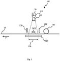
- Fig. 1 shows schematically a side view of a device 100 for observing and / or inspecting a material web 10.
- the device 100 can be used for all of the methods described below for observation and / or Inspection of a web of material can be used. In addition to web monitoring / inspection, the device can also be used for color density measurement or spectral color measurement.
- the device 100 comprises a camera 110 which is equipped with a matrix chip 20 with a binning function and a “Region of Interest” (ROI) function, for example a CCD or CMOS sensor.
- the camera 110 can be suitable for 1D, 2D and / or 3D recordings and can be a color or black-and-white camera.
- the camera 110 or the field of view of the camera 110 can either be parallel or traversing in relation to the direction of the material web width (corresponding to the direction x in Fig. 2 based on the correspondingly arranged matrix chip 20 shown).
- Fig. 1 also shows different devices for illuminating the material web 10. In the example shown, one or two lighting devices 130 are provided above the material web 10 and one lighting device 120 is provided below the material web 10. Alternative embodiments can also have only one lighting device or more than two lighting devices, so that different types of lighting can be used to illuminate the material web 10 for all the recordings or combinations of recordings described below.
- a sensor 140 can be provided which, for example, measures the distance covered or the current speed of the material web.
- encoders, proximity switches, print mark sensors and direct speed sensors can be used as sensors.
- rotary encoders incrementmental rotary encoders or rotary pulse encoders
- the impeller with a known rolling circumference sits on the material web and, for example, one or more pulses per revolution are generated.
- the distance covered by the material web in the direction of the material web length y can be determined from the number of detected pulses.
- the material web speed can then, for example, via the number of detected pulses per unit of time and via the covered Path determined, i.e. determined using the values of time and path.
- the material web is preferably moved in the direction of a material web length y, but can also be moved in the direction of a material web width x.
- the material web 10 can be moved, for example, at a web speed of at least 150 m / min, in particular at least 500 m / min, preferably at least 900 m / min, in the direction of the material web length y.
- the device 100 also comprises a (in Fig. 1 control unit (not shown) that controls all activities of the device and processes corresponding signals, for example from sensor 140 or other external sensors.
- the control unit can comprise a computer unit or be part of a computer unit or a test unit.
- one or more monitors can be provided to visually display the recordings of the camera or the image sequences created (in Fig. 1 not shown).
- Fig. 2 shows schematically a matrix chip 20 and serves to explain the binning function of the matrix chip 20.
- Binning is understood to mean the combination of adjacent physical pixels already on the matrix chip 20 itself to form a virtual pixel.
- a higher light sensitivity per virtual image point can be achieved on the one hand (for example to improve the signal-to-noise ratio).
- the image resolution is reduced in accordance with the number of combined pixels, which makes the image coarser.
- a lower image resolution has the advantage that the bandwidth can be reduced when transmitting the data of a recording to a subsequent processing system.
- a smaller amount of data per recording also allows the image recording frequency ("frames per second" - FPS) to be increased.
- Fig. 2 five different binning stages are now exemplarily shown (whereby the total number of pixels of the matrix chip 20 is to be understood purely schematically): starting from top left to bottom right no binning or a 1x1 binning 1, a 2x2 binning 2, a 3x3 binning 3, a 4x4 binning 4 and a 5x5 binning 5, with 1, 4, 9, 16 and 25 physical pixels respectively being combined into one virtual pixel.
- the physical pixels of the matrix chip 20 can be moved along a first direction, in particular along the direction of the material web length y, along a second direction, in particular along the direction of the material web width x or combined along the first direction and the second direction can be combined.
- the binning or the binning stages can be freely determined, so that the matrix sensor 20 can be designed, for example, that when using binning stages of the binning function, the pixels of the matrix chip 20 are combined so that virtual pixels with a Pixel size of 1x2, 1x3, 1x4, 1x5, 1x6, 1x7, 1x8, 1x9, 1x10, 1x11, 2x1, 3x1, 4x1, 5x1, 6x1, 7x1, 8x1, 9x1, 10x1, 11x1, 2x2, 3x2, 2x3, 4x2, 2x4, 5x2, 2x5, 6x2, 2x6, 7x2, 2x7, 8x2, 2x8, 9x2, 2x9,10x2, 2x10, 11x2, 2x11, 3x3, 4x3, 3x4, 5x3, 3x5, 6x3, 3x6, 7x3, 3x7, 8x3, 3x8, 9x3, 3x9, 10x3, 3x10, 11x3, 3x11, 4x4, 5x4, 4x5, 6x4, 4
- the distribution / number of the combined pixels can be freely determined depending on the application and the maximum physical resolution of the matrix chip 20 used and is limited purely by the physical resolution of the matrix chip 20 used. This is to be seen in particular with regard to the rapid further development in the field of matrix sensors and the possible data transmission rates, so that the methods and devices described here are by no means limited to the currently available matrix sensors / data rates.
- the method according to the invention uses the binning function of the matrix chip 20 in a new way and enables a physical zoom function without further complex devices such as additional movable cameras or zoom lenses. This is made possible by the following procedure: creating a first recording of a first section of a material web 10 at a first point in time with the camera 110 (which includes the matrix chip 20 with a binning function) and creating it a second recording of a second section of the material web 10 at a second point in time with the camera 110.
- a first binning stage is used for the first recording, in which a first number of pixels of the matrix chip 20 is combined using the binning function and a second binning stage is used for the second recording, in which a second number of pixels of the matrix chip 20 are combined using the binning function.
- the first number of pixels that are respectively combined is higher or lower than the second number of pixels that are respectively combined, whereby a physical zoom function is achieved for the second recording.
- a first example is web monitoring, in which recordings with as constant a resolution as possible are continuously observed using the zoom levels.
- the zoom level used can, for example, be specified or it can take place in accordance with an input by a user. This means that a user can specify the zoom level to be selected with which the recordings are made.
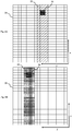
- Figures 3A and 3B shown Figure 3A shows a point in time of a recording in which the complete field of view (first active area 22) of the matrix chip 20 is used with a first binning stage, for example to record a first section of a material web.
- a reduced viewing area is recorded (with a second, smaller active area 24 of the matrix chip 20).
- a lower binning level is then selected with an image resolution that remains as constant as possible for the reduced viewing area (based on the original viewing area), which also means a larger number of pixels per mm for the reduced viewing area.
- Figure 3B shows Two consecutive recordings do not necessarily always have to have a different binning level. It can happen that a large number of recordings are made with the first binning level and the user is only made a second recording with the second binning level in the event of certain events, for example because he has discovered an error. Also, after recordings have been made “zoomed in", the user can "zoom out” again to get a larger one To be able to observe the field of view of the matrix chip 20 and thus a larger section of the material web.
- the material web 10 can, for example, have repetitive repeats, with a corresponding trigger signal being provided for each repeat during web monitoring, so that the first point in time of the first recording can be determined by a first trigger signal and the second point in time of the second recording can be determined by a second trigger signal.
- the user it is also possible for the user to adjust the X-Y coordinates during web observation, so that the sections do not represent sections of the material web 10 that correspond or not completely.
- control unit or a control device can be used for triggering, which for this purpose receives information from the sensor 140 in order to send a trigger signal for the first recordings and the second recordings to the camera 110.
- the control unit or the control device can be provided as an external device.
- the sensor 140 can be connected directly to the control device or to the camera 110.
- a second example for the application of the device and method according to the invention is inspection.
- second recordings are automatically made with the second binning stage in order to be able to inspect the defect more precisely.
- the first section and the second section can be two identical material web sections or the second section can be a partial section of the first section.
- a first active area 22 of the matrix chip 20 can be used for the first recording in order to cover a first viewing area and a second active area 24 of the matrix chip 20 can be used for the second recording in order to cover a second viewing area.
- the first active area 22 and correspondingly the first viewing area can be larger than the second active area 24 and correspondingly the second viewing area.
- the second active area 24 can be the same size as the first active area 22 (see FIG Figures 4A, 4B ).
- the second active area 24 can be part of the first active area 22, in particular lie within the first active area 22 (see FIG Figures 3A, 3B ).
- One advantage of this method is, for example, the reduction of the amount of data and the required computing power through the use of the binning function and a "Region of Interest" (ROI) function, since only the required resolution or the required viewing area is queried or recorded and is processed.
- ROI Region of Interest
- a reduced data load in turn, also allows the image recording frequency (FPS) to be increased.
- the viewing areas of the camera 110 or the matrix chip 20 can, for example, have a length and a width which are arranged according to the direction of the material web length y and the direction of the material web width x (the directions x and y are in the Figures 2 to 6C shown).
- the length and / or the width of the viewing area are changed.
- the principle of the "Region of Interest" (ROI) is used here, which makes use of the fact that it is possible to activate only certain areas 22, 24 of the sensor in the case of matrix chips 20: for the first recording, for example, this can entire field of view of the matrix sensor 20 (see Figure 3A ) or a large part of the field of view can be used.
- a first binning stage is used for this part, which combines a relatively large number of physical pixels into one virtual pixel.
- a correspondingly selected second area 24 of the matrix chip 20 can be used to cover a second (smaller) field of view (one ROI is selected).
- a second level of binning is used for this part, the combines relatively few physical pixels into one virtual pixel or the binning is completely dissolved (1x1 binning level).
- the field of view can also be the same for both recordings (see e.g. Figures 4A, 4B ).
- a second binning stage is selected in which, compared to the first binning stage, only a smaller number of physical pixels is combined for the first exposure or no binning at all more is applied.
- the second recording would have a higher image resolution (number of pixels per mm) with the same size field of view, so that the second recording would be displayed more precisely or, for example, a better physical resolution for a digital zoom function could be made possible.
- one camera and one lens can be saved (an example of this below) .
- a correspondingly smaller 24 or larger area 22 is activated here in the same ratio in the X and Y directions from the outside to the inside (or from the inside to the outside), depending on that of which zoom level should be changed to which zoom level.
- the drawings of the figures are to be understood here purely as examples.
- Figure 3A with regard to the matrix chip area in the x and y directions) of the matrix chip 20 is mostly fully utilized in the path observation and is only limited to an area 24 when zooming in.
- the possible zoom levels it can also be described as follows: the more physical pixels were combined into a virtual pixel for the first recording, the more physical zoom levels are available for the second recording, in which fewer physical pixels are then added in a lower binning level a virtual pixel or the binning function is no longer used and the maximum physical resolution of the matrix chip 20 is used.
- the result is similar to an optical zoom, since there is no need to extrapolate algorithmically, as is the case with digital zoom, for example, but the information gain is achieved physically. If the binning function is no longer used or the maximum physical resolution of the matrix chip 20 is used, a further digital zoom function can of course also take place, but with the known disadvantages that result from the digital zoom function.
- the resolution of 1024x768 pixels of the sensor remains constant over the optical zoom.
- the image resolution is 0.098 mm / pixel
- the minimum viewing area approximately 0.009 mm / pixel.
- the zoom lens even provides a better image resolution in mm / pixel in the minimal field of vision thanks to the constant resolution of 1024x768 pixels.
- the zoom lens is to be saved, but the claim that the quality of the recordings is retained for the respective viewing areas is retained. According to the invention, this could be achieved, for example, with a matrix chip with 100 megapixels (resolution for example 11548x8661). With a binning level with 11x11 binning and a corresponding maximum field of view of approx. 100 mm x 71 mm, you get an image resolution of approx. 0.095 mm / virtual pixel. If you want to take a picture according to zoom level 12 of the 12x zoom lens, the binning function can be canceled (corresponds to the 1x1 binning level) and the field of view limited to approx. 9 mm x 7 mm.
- the image resolution is approx. 0.046 mm / pixel.
- the image resolution is only obtained for the field of vision through the sensor with wide-angle lens (first camera).
- it is digitally zoomed up to a field of view of e.g. 32 mm x 24 mm.
- Digital zooming is then done again up to the field of view of approx. 4 mm x 3 mm. This means that the resolution for the respective field of view is not kept constant, as is the case with a web monitoring system with a zoom lens.
- the principle of the invention By applying the principle of the invention, one camera and one lens are to be saved here, but the claim that the quality of the recordings is retained for the respective viewing areas is retained. According to the invention, this can be achieved, for example, with a matrix chip with 70 megapixels (resolution, for example 9735x7920).
- the matrix chip is binned for the maximum viewing area of 120 mm x 90 mm with a 4x4 binning level, so that a physical or virtual resolution (by combining physical pixels in the 4x4 binning level) of approx. 2434x1823 pixels is created, which corresponds to approx. 0.049 mm / virtual pixel. From here it could theoretically be possible to digitally zoom in to a field of view of 32 mm x 24 mm.
- the binning level would be set to 1x1 or the binning would be completely canceled.
- the matrix chip then has an equivalent resolution of 2596 x 1944 pixels as the sensor of the second camera with telephoto lens of the known system, which corresponds to approx. 0.012 mm / pixel. From here, digital zooming would take place again, up to a field of view of at least 4 mm x 3 mm.
- the image resolution mm / pixel would then be in the field of view 120 mm x 90 mm to 32 mm x 24 mm always at 0.049 mm / pixel and from 32 x 24 mm to 4 mm x 3 mm also always at 0.012 mm / pixel, since the smaller the viewing area, the smaller the resolution.
- the unused binning levels 3x3 and 2x2 could still be used from a certain viewing area in order to get better physical resolution values earlier.
- the second binning level and, optionally, the second viewing area can be selected depending on the user input. If a digital zoom is used, this can also be selected depending on the user input. This means that the number of pixels that are combined in the second binning stage (more or less than in the first binning stage for the first exposure) as well as the position and size of the viewing area (ROI) can be user-controlled.
- the first active area 22 and the second active area 24 of the matrix chip 20 are not identical or may or may not overlap. In addition, several trigger signals are output per report, since a 100% inspection of the material web 10 takes place.
- the method then includes evaluating the first recording and determining a position of at least one flaw 26 on the material web 10. The second binning stage and / or the second active area 24 can then be determined based on the position of the flaw 26.
- Figures 4A and 4B show an example with a first active area 22 in which the error 26 was detected (see 4A).
- Figure 4B represents the matrix chip 20 for the second recording at the second point in time at which the material web has moved a little further in the y-direction.
- the second active area 24 is now used in a smaller binning stage and thus with a greater resolution in order to be able to record or represent and inspect the defect 26 more precisely.
- the method is particularly beneficial in inspection, if not just the binning stage for the second active area 24 is changed as in FIG Figures 4A and 4B shown, but also the field of vision in the x and y directions can be restricted to the position of the fault. This is in Figures 5A and 5B shown schematically. It is then possible, for example, to reduce the binning level even further and thus achieve a higher resolution for the zoom function without increasing the amount of data in the recording.
- the binning function is resolved for at least one area of the matrix chip 20 or the binning level is reduced and the ROI is optionally selected by selecting the second active area 24 so that a field of view of the camera results for the second recording a subsequent second recording of the error 26 or (several recordings of the errors 26a, 26b, see Figures 6A to 6C ) with a higher resolution, which can then be stored or displayed for a user, for example.
- the second recording can also be made at the second point in time based on the position of the error 26.
- the position of the error 26 can be determined, for example, in coordinates based on the direction of the material web length y and the direction of the material web width x. Based on these coordinates and the web speed of the material web 10 (for example measured by the sensor 140), the second point in time for the second recording can then be determined.
- the second active area 24 can also be determined as a function of a material web speed. For the second active area 24, its position in the direction of the material web length y, in the direction of the material web width x and / or a size based on the position of the flaw 26 and the size of the flaw 26 can be determined.
- the second exposure focuses specifically on the defect area concentrated.
- the data load can be further reduced and the resolution increased, since only a small area of the matrix chip 20 has to be activated with a reduced or resolved binning function. That is, the first and the second active area 24 as well as the adaptation of the binning level (or the complete dissolution of the binning) can be adapted variably.
- an image recording for web monitoring can also take place.
- the principle according to the invention can also be used, for example, for a variable error classification, in which it is also possible to set the error size to be detected downwards (or upwards) during operation.
- inspection systems actually specify the approximate defect size up to which they can even inspect or recognize defects.
- the resolution for the first active area 22 could be increased (if the hardware allows this) so that even smaller errors can be detected which are then included in the second active area 24 by means of the second recording even higher resolution can be recorded.
- this is of course also possible: if certain error sizes can be tolerated, then the resolution for the first active area 22 can also be reduced.
- the resolution used for the first active area 22 can therefore be used to set directly the size of the defect from which the defects can be recognized. If an error is detected, this is then recorded in the second active area 24 by means of the second recording with a higher resolution.
- the device can also comprise a material web position sensor which, for example, determines a position or a width of the material web (in the x direction).
- the signals of the position sensor can be provided to the control unit so that the active areas 22, 24 of the matrix sensor are determined based thereon, in particular a size and / or a position of the active areas 22, 24 in the direction of the material web width x are set.
- the position of a plurality of defects 26a, 26b can of course also be determined and a corresponding plurality of second recordings can be made. If the two or more defects 26a, 26b have the same position in the direction of the material web length y, then these two or more defects 26a, 26b can also be recorded simultaneously in a second recording with the correspondingly higher resolution.
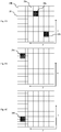
- the matrix chip 20 is divided into first and second parts 20a, 20b, the first part 20a working with the first binning stage and being used for the first recording and the second part 20b working with the second binning stage and for the second recording is used.
- the second part 20b lies behind the first part 20a in the direction of the movement of the material web. It can then be provided, for example, that the second part 20b is only activated if an error 26a, 26b was found in the first recording.
- the first part 20a can be larger than the second part 20b.
- the first part 20a can, for example, be at least twice as large, at least three times as large, at least five times as large, or at least nine times as large as the second part 20b.
- the first part 20a can, for example, take up approximately 90% of the matrix chip 20 and the second part 20b take up approximately 10% of the matrix chip 20.
- It can also be advantageous to increase the camera parameter “gain” for the second part 20b in order to compensate for a poorer light yield in this less binned state or to reduce the image noise.
- the "Gain" camera parameter can be increased or adapted to a certain binning level in order to compensate for a possibly poorer light yield.
- first recordings can be made continuously with the first part 20a and second recordings with the second part 20b.
- the second recordings can be stored continuously in a ring memory.
- Corresponding second recordings can be read out from the ring buffer and / or made available to a user and / or displayed on a monitor, for example, if so At least one error 26a, 26b was found in corresponding first recordings.
- Both the first recordings and the second recordings can cover 100% of the material web 10. In order to cover 100% of the material web 10, the number of second receptacles must be adapted in accordance with the proportions of the first and second parts 20a, 20b.
- the first part 20a takes up, for example, 90% of the matrix chip 20 and the second part 20b takes up 10% of the matrix chip 20
- a total of nine second recordings must be made with the second part 20b for each first exposure with the first part 20a .
- the second part 20b has to be triggered nine times for nine recordings, while the first part 20a only has to be triggered once.
- an image sequence with a lower binning level or without the use of binning (which is equivalent to a higher physical resolution) can be produced, which also covers 100% of the material web 10.
- the first part 20a has a binning level of 9x9 and the second part 20b has a binning level of 1x1 (i.e. practically no binning is used)
- this procedure is advantageous because the individual data packets (from the first and second recordings) always contain an equivalent data size that can be matched to an available bandwidth. The available bandwidth will then not be exceeded at any time.
- a suitable ratio of the parameters size ratio of the first part 20a to the second part 20b of the matrix chip 20 and the binning level used for the respective parts
- Figure 6A a recording of the first part 20a is shown, in which two errors 26a, 26b were detected.
- Figure 6B show a recording with the second part 20b at a point in time at which the first flaw 26a is in the field of view of the second part 20b.
- Figure 6C shows a further recording with the second part 20b at a later point in time at which the second defect 26b is in the field of view of the second part 20b.
- Another advantage of this method or this device 100 is that it is also possible to display one-off errors with high resolution do not necessarily have to be repetitive errors.
- the ROI in the y-direction and optionally also in the x-direction
- the binning level are adjusted and the same error is recorded again with high resolution will.
- the digital zoom function can, for example, cover transition areas in the resolution between corresponding binning levels. This is advantageous in the method described here, since the physical resolution can be adapted again and again through the binning stages, so that a deterioration due to the use of the digital zoom is barely noticeable. In other words: even before an image looks blurred or pixelated due to excessive digital zoom and corresponding interpolation (e.g. when displayed on a monitor), the next binning level can be used, which again provides a higher physical resolution.
- the digital zoom function can also still be used after the binning levels have been completely resolved, i.e. the physical zoom function has been exhausted.
- the selection of the binning levels and the areas to be activated can be determined relatively freely.
- the active areas 22, 24 of the matrix chip 20 and the binning steps, and optionally the use of a digital zoom to be coordinated for the first and second recordings in such a way that a stepless zoom function is provided will.
- the selected viewing areas and the binning levels are adapted to one another in such a way that, for example, the same resolution (based on the total number of (virtual) pixels per viewing area) is given for each viewing area is.
- the binning levels can also be adapted in such a way that the resolution is reduced in a constant field of view, for example in order to increase the image recording frequency (FPS).
- FPS image recording frequency
- a resolution of 2048 x 1024 is used, then 56 FPS can be sent to the control unit via a single gigabit Ethernet interface.
- the resolution of 2048 x 512 is used instead (e.g. through 1x2 binning or by restricting the field of view), then 112 FPS can be sent to the control unit via the single gigabit Ethernet interface.
- the FPS and the field of view then ultimately again determine the maximum possible web speed for a 100% inspection of the material web 10.
- the respective active areas 22, 24 and thereby the respective viewing area and the binning level to be used can be optimally coordinated with one another depending on a maximum physical resolution of the matrix chip 20, the web speed and the properties of an objective 112 optionally used for the recordings will.
- the properties of the optionally used objective can also be adapted as a function of the maximum physical resolution of the matrix chip 20.
- the matrix chip 20 can, for example, have a resolution of at least 16 megapixels, at least 32 megapixels, at least 50 megapixels, at least 70 megapixels or at least 100 megapixels. There is no upper limit to be seen here, particularly due to the rapid development in this area.
- An additional recording of the first section is created at a third point in time using the first binning stage, a different active area of the matrix chip 20 being used for the additional recording of the first section than for the first recording of the first section.
- the third point in time is after the first point in time.
- the third point in time is before the second point in time or after the second point in time, depending on the application.
- For the two recordings of the first section will be different types of illumination are used to illuminate the material web 10, so that two different image sequences (with two different types of illumination) of the complete material web 10 can be created.
- an additional recording of the second section is then made at a fourth point in time using the second binning stage, a different active area of the matrix chip 20 being used for the additional recording of the second section than for the first recording of the second section.
- the fourth point in time is after the second or after the third point in time.
- the same type of lighting can be used for the additional recording of the second section as for the additional recording of the first section, in particular a different type of lighting than for the second recording of the second section. In sum, this would then mean, for example: continuously one recording with first illumination and low resolution, first illumination and high resolution, second illumination and low resolution and second illumination with high resolution.
- different types of lighting can thus be used to illuminate the material web 10.
- the multi-inspection is not limited to two images per section with two types of lighting.
- the device can also be used for a multi-inspection with three or more image sequences.
- further recordings of the corresponding sections are then made at corresponding further points in time using corresponding further active areas of the matrix chip 20.
- further types of lighting can be used to illuminate the material web 10.
- the types of lighting can be selected, for example, from the group consisting of reflected-light illuminations, background illuminations and transmitted-light illuminations.
- a range of lighting properties can be implemented: homogeneous or inhomogeneous lighting, direct, diffuse, focused or collimated lighting, coaxial, transmissive and / or polarized lighting, different lighting angles and brightfield or darkfield lighting, light wavelengths in the UV, visible or IR range (around e.g. to be able to inspect security features), single-colored (monochrome), multi-colored (polychrome) or color-coordinated or controllable (RGB) lighting, area lighting or line lighting, constant or flashed lighting, with incident and transmitted lighting, these can be used alternately or at the same time come.
- the lighting devices can be designed as a tunnel lighting system, tube lighting system or dome lighting system, as well as being modular or adapted to the width of the material web.
- incandescent lamps for example, incandescent lamps, gas discharge lamps, LED lighting, OLED lighting or laser lighting can be used as light sources.
- the respective types of lighting and properties can be used, for example, for the following multi-inspection: print image inspection with visible incident light, label inspection with visible transmitted light and inspection of UV security features with UV incident light.
- the image recording for web monitoring can, for example, already take place with the image sequence of the 100% inspection or the image of the 100% inspection can be output as an image for web monitoring.
- the output image then corresponds to the resolution that was used for the inspection. If an extra image recording of the web observation is made with the first and / or second illumination, the field of view and the image resolution can again be adapted accordingly and thus physically zoomed.
- the device can also have a plurality of cameras 110, each of which has a matrix chip with a binning function and an ROI function, each of the cameras producing corresponding recordings for the web monitoring and / or inspection methods described above.
- the cameras can be arranged distributed over the material web width x, so that the viewing areas of the cameras adjoin or overlap one another in the direction of the material web width x.
- a coherent recording can be determined from the recordings of the plurality of cameras 110.
- mechanical offsets of the cameras in the direction of the material web length y to one another can be compensated for by a corresponding selection of active areas of the matrix chips 20.
- the camera array can thus capture a continuous material web section which is positioned identically in the direction of the material web length y.
- At least one camera 110 can also be provided on the front side of the material web 10 and at least one camera on a rear side of the material web 10, each of the cameras again corresponding recordings for the web monitoring method described above and / or inspection. This enables the observation or inspection of both sides of the material web.
Landscapes
- Engineering & Computer Science (AREA)
- Physics & Mathematics (AREA)
- General Physics & Mathematics (AREA)
- Analytical Chemistry (AREA)
- General Health & Medical Sciences (AREA)
- Health & Medical Sciences (AREA)
- Life Sciences & Earth Sciences (AREA)
- Chemical & Material Sciences (AREA)
- Pathology (AREA)
- Biochemistry (AREA)
- Immunology (AREA)
- Signal Processing (AREA)
- Textile Engineering (AREA)
- Multimedia (AREA)
- Computer Vision & Pattern Recognition (AREA)
- Theoretical Computer Science (AREA)
- Quality & Reliability (AREA)
- Investigating Materials By The Use Of Optical Means Adapted For Particular Applications (AREA)
Applications Claiming Priority (1)
| Application Number | Priority Date | Filing Date | Title |
|---|---|---|---|
| DE102016220757.1A DE102016220757A1 (de) | 2016-10-21 | 2016-10-21 | Verfahren und Vorrichtung zur Materialbahnbeobachtung und Materialbahninspektion |
Publications (2)
| Publication Number | Publication Date |
|---|---|
| EP3312596A1 EP3312596A1 (de) | 2018-04-25 |
| EP3312596B1 true EP3312596B1 (de) | 2021-11-17 |
Family
ID=60083792
Family Applications (1)
| Application Number | Title | Priority Date | Filing Date |
|---|---|---|---|
| EP17195965.3A Active EP3312596B1 (de) | 2016-10-21 | 2017-10-11 | Verfahren und vorrichtung zur materialbahnbeobachtung und materialbahninspektion |
Country Status (6)
| Country | Link |
|---|---|
| US (1) | US10878552B2 (ko) |
| EP (1) | EP3312596B1 (ko) |
| JP (2) | JP7266362B2 (ko) |
| KR (1) | KR102416273B1 (ko) |
| CN (1) | CN107976450B (ko) |
| DE (1) | DE102016220757A1 (ko) |
Families Citing this family (13)
| Publication number | Priority date | Publication date | Assignee | Title |
|---|---|---|---|---|
| EP3502637A1 (en) * | 2017-12-23 | 2019-06-26 | ABB Schweiz AG | Method and system for real-time web manufacturing supervision |
| JP6927124B2 (ja) | 2018-03-30 | 2021-08-25 | 東洋紡株式会社 | 熱収縮性ポリエステル系フィルム |
| JP2020000578A (ja) * | 2018-06-29 | 2020-01-09 | 株式会社三洋物産 | 遊技機 |
| JP2020000577A (ja) * | 2018-06-29 | 2020-01-09 | 株式会社三洋物産 | 遊技機 |
| JP2020000581A (ja) * | 2018-06-29 | 2020-01-09 | 株式会社三洋物産 | 遊技機 |
| JP2020000580A (ja) * | 2018-06-29 | 2020-01-09 | 株式会社三洋物産 | 遊技機 |
| EP3661191A1 (de) * | 2018-11-27 | 2020-06-03 | B&R Industrial Automation GmbH | Verfahren zum auslesen eines flächensensors |
| KR102629343B1 (ko) | 2018-12-21 | 2024-01-26 | 삼성전자주식회사 | 다중 셀 구조의 카메라 모듈 및 그 카메라 모듈을 포함하는 휴대용 통신 장치 |
| US20200371040A1 (en) * | 2019-05-21 | 2020-11-26 | Industrial Maintenance Engineering, Inc. d/b/a AIS Gauging | Static full width measurement system |
| US11218641B2 (en) * | 2019-09-09 | 2022-01-04 | Qualcomm Incorporated | Image capture mode adaptation |
| CN111586289A (zh) * | 2020-03-31 | 2020-08-25 | 广东利元亨智能装备股份有限公司 | 一种高速飞拍控制方法及系统 |
| JP2022049436A (ja) * | 2020-09-16 | 2022-03-29 | 東洋製罐グループホールディングス株式会社 | 表面検査システム |
| KR20240040057A (ko) * | 2022-08-05 | 2024-03-27 | 코어포토닉스 리미티드 | 자동 조정 가능한 줌 시야를 갖는 줌 디지털 카메라용 시스템 및 방법 |
Citations (1)
| Publication number | Priority date | Publication date | Assignee | Title |
|---|---|---|---|---|
| US20120013733A1 (en) | 2010-07-15 | 2012-01-19 | Eltromat Gmbh | Apparatus for Monitoring a Print Result in a Rotary Printing Press |
Family Cites Families (29)
| Publication number | Priority date | Publication date | Assignee | Title |
|---|---|---|---|---|
| JPH0686183A (ja) * | 1992-08-31 | 1994-03-25 | Canon Inc | 固体撮像素子 |
| JPH11248641A (ja) * | 1998-03-03 | 1999-09-17 | Sumitomo Metal Ind Ltd | 表面欠陥検査装置及び表面欠陥検査方法 |
| AT406528B (de) * | 1998-05-05 | 2000-06-26 | Oesterr Forsch Seibersdorf | Verfahren und einrichtung zur feststellung, insbesondere zur visualisierung, von fehlern auf der oberfläche von gegenständen |
| SE523681C2 (sv) * | 2002-04-05 | 2004-05-11 | Integrated Vision Prod | System och sensor för avbildning av egenskaper hos ett objekt |
| JP4151948B2 (ja) * | 2002-11-07 | 2008-09-17 | 住友化学株式会社 | 帯状被検体の検査システム及び検査プログラム |
| US7257278B2 (en) * | 2003-02-26 | 2007-08-14 | Hewlett-Packard Development Company, L.P. | Image sensor for capturing and filtering image data |
| US20050226466A1 (en) * | 2004-04-06 | 2005-10-13 | Quad/Tech, Inc. | Image acquisition assembly |
| US7688364B2 (en) * | 2004-12-10 | 2010-03-30 | Ambarella, Inc. | Decimating and cropping based zoom factor for a digital camera |
| FI119708B (fi) * | 2006-02-01 | 2009-02-13 | Viconsys Oy | Laite rainan tarkkailemiseksi |
| JP4655991B2 (ja) * | 2006-04-21 | 2011-03-23 | カシオ計算機株式会社 | 撮像装置及び電子ズーム方法と、プログラム |
| JP2008172506A (ja) * | 2007-01-11 | 2008-07-24 | Nec Corp | イメージセンサ |
| DE102007055820A1 (de) * | 2007-12-14 | 2009-06-18 | Voith Patent Gmbh | Verfahren und Vorrichtung zur Erfassung zumindest einer die Eigenschaften einer Oberfläche in einer Materialbahnbehandlungseinrichtung wenigstens mittelbar charaktersierenden Größe und Verfahren zur Optimierung der Betriebsweise einer Materialbahnbehandlungseinrichtung |
| DK2003443T3 (da) * | 2008-02-11 | 2011-09-05 | Texmag Gmbh Vertriebsges | Apparat til registrering af et billede |
| FR2936605B1 (fr) * | 2008-10-01 | 2014-10-31 | Saint Gobain | Dispositif d'analyse de la surface d'un substrat |
| DE102009029081A1 (de) * | 2009-09-02 | 2011-03-03 | Voith Patent Gmbh | Lasermarkierung |
| US20110141269A1 (en) * | 2009-12-16 | 2011-06-16 | Stephen Michael Varga | Systems And Methods For Monitoring On-Line Webs Using Line Scan Cameras |
| CN102483324A (zh) * | 2010-03-23 | 2012-05-30 | 富士胶片株式会社 | 拍摄装置及其控制方法,以及三维信息测量装置 |
| FI20106053A0 (fi) * | 2010-10-13 | 2010-10-13 | Metso Automation Oy | Järjestelmä rainan tarkkailemiseksi ja vastaava menetelmä rainan tarkkailemiseksi |
| US20130208978A1 (en) * | 2010-10-19 | 2013-08-15 | 3M Innovative Properties Company | Continuous charting of non-uniformity severity for detecting variability in web-based materials |
| ES2793373T3 (es) * | 2010-12-30 | 2020-11-13 | Alltec Angewandte Laserlicht Tech Gesellschaft Mit Beschraenkter Haftung | Aparato sensor |
| JP5983616B2 (ja) * | 2011-09-13 | 2016-09-06 | 日本電気株式会社 | 撮像装置、撮像方法及びプログラム |
| DE102012101310C5 (de) | 2012-02-17 | 2014-09-04 | Stephan Krebs | Vorrichtung und Verfahren zur Druckbildkontrolle |
| KR101205128B1 (ko) * | 2012-05-11 | 2012-11-26 | 주식회사 앤비젼 | 이미지 센서 비닝 기법을 이용하여 이미지 센서의 픽셀당 해상도를 조정하는 광학 검사 장치 |
| CN102721702A (zh) * | 2012-06-27 | 2012-10-10 | 山东轻工业学院 | 基于嵌入式处理器的分布式纸病检测系统及方法 |
| CN105358966B (zh) * | 2013-05-23 | 2019-08-02 | 材料开发中心股份公司 | 对长材进行表面检查的方法及执行这样的方法的设备 |
| CN104422698B (zh) * | 2013-09-04 | 2017-03-29 | 昆山钞票纸业有限公司 | 随动式防伪纸定位施放荧光纤维在线检测装置 |
| JP2015105930A (ja) * | 2013-12-02 | 2015-06-08 | 旭硝子株式会社 | 透光性基板の微小欠陥検査方法および透光性基板の微小欠陥検査装置 |
| CN104713483B (zh) * | 2015-03-30 | 2017-09-12 | 昆山钞票纸业有限公司 | 防伪纸内嵌光敏纤维的检测方法和装置 |
| CN105203557B (zh) * | 2015-10-28 | 2018-06-08 | 江西洁美电子信息材料有限公司 | 一种电子纸带造纸质量在线检测系统 |
-
2016
- 2016-10-21 DE DE102016220757.1A patent/DE102016220757A1/de active Pending
-
2017
- 2017-10-11 EP EP17195965.3A patent/EP3312596B1/de active Active
- 2017-10-18 KR KR1020170135385A patent/KR102416273B1/ko active IP Right Grant
- 2017-10-19 US US15/788,333 patent/US10878552B2/en active Active
- 2017-10-19 CN CN201710979576.0A patent/CN107976450B/zh active Active
- 2017-10-20 JP JP2017203346A patent/JP7266362B2/ja active Active
-
2022
- 2022-03-22 JP JP2022045740A patent/JP7311665B2/ja active Active
Patent Citations (1)
| Publication number | Priority date | Publication date | Assignee | Title |
|---|---|---|---|---|
| US20120013733A1 (en) | 2010-07-15 | 2012-01-19 | Eltromat Gmbh | Apparatus for Monitoring a Print Result in a Rotary Printing Press |
Also Published As
| Publication number | Publication date |
|---|---|
| KR102416273B1 (ko) | 2022-07-05 |
| KR20180044198A (ko) | 2018-05-02 |
| US10878552B2 (en) | 2020-12-29 |
| JP7266362B2 (ja) | 2023-04-28 |
| CN107976450A (zh) | 2018-05-01 |
| CN107976450B (zh) | 2021-10-29 |
| JP2022091853A (ja) | 2022-06-21 |
| US20180114308A1 (en) | 2018-04-26 |
| JP2018066740A (ja) | 2018-04-26 |
| JP7311665B2 (ja) | 2023-07-19 |
| DE102016220757A1 (de) | 2018-04-26 |
| EP3312596A1 (de) | 2018-04-25 |
Similar Documents
| Publication | Publication Date | Title |
|---|---|---|
| EP3312596B1 (de) | Verfahren und vorrichtung zur materialbahnbeobachtung und materialbahninspektion | |
| DE102008018225B4 (de) | Optischer Navigationsschaltkreis einer optischen Maus, dynamisches Rekonfigurationsverfahren für ein Pixelarray sowie Vorrichtung | |
| EP3729137B1 (de) | Multipuls-lidarsystem zur mehrdimensionalen erfassung von objekten | |
| DE102004010854A1 (de) | Anzeigen von Netzsegmentdecodierinformationen in schematischer Form | |
| DE102009043747A1 (de) | Verfahren zur Erzeugung eines Mikroskopbildes und Mikroskop | |
| EP2186639B1 (de) | Verfahren und Vorrichtung zum Überprüfen eines Druckbildes auf einer laufenden Materialbahn | |
| EP2557451B1 (de) | Verfahren und anordnung zur optischen erfassung einer beleuchteten probe | |
| DE102014008686B4 (de) | Verfahren und Vorrichtung zur Farbinterpolation | |
| EP2534521A1 (de) | Verfahren und vorrichtung zum einstellen eines geeigneten auswerteparameters für ein fluoreszenzmikroskop | |
| DE102009059977A1 (de) | Endoskopsystem mit Abtastfunktion | |
| EP1542051A1 (de) | Verfahren und Vorrichtung zum Trennen unterschiedlicher Emissionswellenlängen in einem Scanmikroskop | |
| WO2019086686A1 (de) | Reduktion von bildstörungen in bildern | |
| DE102005062237A1 (de) | Verfahren und Vorrichtung zur Untersuchung des Abbildungsverhaltens einer Abbildungsoptik | |
| WO2012084531A1 (de) | Kamera mit einem farbbildsensor sowie aufnahmeverfahren mit einer solchen kamera | |
| DE102006036845B4 (de) | Verfahren und Vorrichtung zum Scannen einer Vorlage mittels einer Zeilenkamera | |
| DE102018222903A1 (de) | Verfahren und Verarbeitungseinrichtung zum Verarbeiten von Messdaten eines Bildsensors | |
| DE112014006356B4 (de) | Verfahren zur Verbesserung der Bildqualität eines Ladungsträgerteilchen-Rastermikroskops und Ladungsträgerteilchen-Rastermikroskop | |
| EP1729258A2 (de) | Verfahren und Vorrichtung zur Ermittlung von Bewegungsvektoren | |
| EP3894929A1 (de) | Mikroskopsystem mit eingabeeinheit zum gleichzeitigen einstellen von wenigstens drei einstellparametern mittels eines in einer eingabefläche positionierbaren eingabezeigers | |
| US20090087117A1 (en) | Filtering circuit, filter processing method, image pickup element circuit and camera | |
| DE102004021047B3 (de) | Verfahren zum Vergleich eines Bildes mit mindestens einem Referenzbild | |
| DE102022002637B3 (de) | Kamerasystem und Verfahren zu dessen Betrieb | |
| EP3312595A1 (de) | Verfahren und vorrichtung zur kompensation eines materialbahnversatzes bei der materialbahninspektion | |
| EP3316216A1 (de) | Verfahren zum prüfen eines gegenstands | |
| DE102022108603A1 (de) | Bildprüfvorrichtung und Bildprüfverfahren |
Legal Events
| Date | Code | Title | Description |
|---|---|---|---|
| PUAI | Public reference made under article 153(3) epc to a published international application that has entered the european phase |
Free format text: ORIGINAL CODE: 0009012 |
|
| STAA | Information on the status of an ep patent application or granted ep patent |
Free format text: STATUS: EXAMINATION IS IN PROGRESS |
|
| 17P | Request for examination filed |
Effective date: 20171011 |
|
| AK | Designated contracting states |
Kind code of ref document: A1 Designated state(s): AL AT BE BG CH CY CZ DE DK EE ES FI FR GB GR HR HU IE IS IT LI LT LU LV MC MK MT NL NO PL PT RO RS SE SI SK SM TR |
|
| AX | Request for extension of the european patent |
Extension state: BA ME |
|
| GRAP | Despatch of communication of intention to grant a patent |
Free format text: ORIGINAL CODE: EPIDOSNIGR1 |
|
| STAA | Information on the status of an ep patent application or granted ep patent |
Free format text: STATUS: GRANT OF PATENT IS INTENDED |
|
| INTG | Intention to grant announced |
Effective date: 20210104 |
|
| GRAJ | Information related to disapproval of communication of intention to grant by the applicant or resumption of examination proceedings by the epo deleted |
Free format text: ORIGINAL CODE: EPIDOSDIGR1 |
|
| STAA | Information on the status of an ep patent application or granted ep patent |
Free format text: STATUS: EXAMINATION IS IN PROGRESS |
|
| INTC | Intention to grant announced (deleted) | ||
| GRAS | Grant fee paid |
Free format text: ORIGINAL CODE: EPIDOSNIGR3 |
|
| STAA | Information on the status of an ep patent application or granted ep patent |
Free format text: STATUS: GRANT OF PATENT IS INTENDED |
|
| GRAP | Despatch of communication of intention to grant a patent |
Free format text: ORIGINAL CODE: EPIDOSNIGR1 |
|
| INTG | Intention to grant announced |
Effective date: 20210630 |
|
| RIN1 | Information on inventor provided before grant (corrected) |
Inventor name: HERRMANN, MARKUS Inventor name: KROEHN, MANFRED |
|
| GRAA | (expected) grant |
Free format text: ORIGINAL CODE: 0009210 |
|
| STAA | Information on the status of an ep patent application or granted ep patent |
Free format text: STATUS: THE PATENT HAS BEEN GRANTED |
|
| AK | Designated contracting states |
Kind code of ref document: B1 Designated state(s): AL AT BE BG CH CY CZ DE DK EE ES FI FR GB GR HR HU IE IS IT LI LT LU LV MC MK MT NL NO PL PT RO RS SE SI SK SM TR |
|
| REG | Reference to a national code |
Ref country code: GB Ref legal event code: FG4D Free format text: NOT ENGLISH |
|
| REG | Reference to a national code |
Ref country code: DE Ref legal event code: R096 Ref document number: 502017012032 Country of ref document: DE |
|
| REG | Reference to a national code |
Ref country code: IE Ref legal event code: FG4D Free format text: LANGUAGE OF EP DOCUMENT: GERMAN |
|
| REG | Reference to a national code |
Ref country code: AT Ref legal event code: REF Ref document number: 1448446 Country of ref document: AT Kind code of ref document: T Effective date: 20211215 |
|
| REG | Reference to a national code |
Ref country code: LT Ref legal event code: MG9D |
|
| REG | Reference to a national code |
Ref country code: NL Ref legal event code: MP Effective date: 20211117 |
|
| PG25 | Lapsed in a contracting state [announced via postgrant information from national office to epo] |
Ref country code: RS Free format text: LAPSE BECAUSE OF FAILURE TO SUBMIT A TRANSLATION OF THE DESCRIPTION OR TO PAY THE FEE WITHIN THE PRESCRIBED TIME-LIMIT Effective date: 20211117 Ref country code: LT Free format text: LAPSE BECAUSE OF FAILURE TO SUBMIT A TRANSLATION OF THE DESCRIPTION OR TO PAY THE FEE WITHIN THE PRESCRIBED TIME-LIMIT Effective date: 20211117 Ref country code: FI Free format text: LAPSE BECAUSE OF FAILURE TO SUBMIT A TRANSLATION OF THE DESCRIPTION OR TO PAY THE FEE WITHIN THE PRESCRIBED TIME-LIMIT Effective date: 20211117 Ref country code: BG Free format text: LAPSE BECAUSE OF FAILURE TO SUBMIT A TRANSLATION OF THE DESCRIPTION OR TO PAY THE FEE WITHIN THE PRESCRIBED TIME-LIMIT Effective date: 20220217 |
|
| PG25 | Lapsed in a contracting state [announced via postgrant information from national office to epo] |
Ref country code: IS Free format text: LAPSE BECAUSE OF FAILURE TO SUBMIT A TRANSLATION OF THE DESCRIPTION OR TO PAY THE FEE WITHIN THE PRESCRIBED TIME-LIMIT Effective date: 20220317 Ref country code: SE Free format text: LAPSE BECAUSE OF FAILURE TO SUBMIT A TRANSLATION OF THE DESCRIPTION OR TO PAY THE FEE WITHIN THE PRESCRIBED TIME-LIMIT Effective date: 20211117 Ref country code: PT Free format text: LAPSE BECAUSE OF FAILURE TO SUBMIT A TRANSLATION OF THE DESCRIPTION OR TO PAY THE FEE WITHIN THE PRESCRIBED TIME-LIMIT Effective date: 20220317 Ref country code: PL Free format text: LAPSE BECAUSE OF FAILURE TO SUBMIT A TRANSLATION OF THE DESCRIPTION OR TO PAY THE FEE WITHIN THE PRESCRIBED TIME-LIMIT Effective date: 20211117 Ref country code: NO Free format text: LAPSE BECAUSE OF FAILURE TO SUBMIT A TRANSLATION OF THE DESCRIPTION OR TO PAY THE FEE WITHIN THE PRESCRIBED TIME-LIMIT Effective date: 20220217 Ref country code: NL Free format text: LAPSE BECAUSE OF FAILURE TO SUBMIT A TRANSLATION OF THE DESCRIPTION OR TO PAY THE FEE WITHIN THE PRESCRIBED TIME-LIMIT Effective date: 20211117 Ref country code: LV Free format text: LAPSE BECAUSE OF FAILURE TO SUBMIT A TRANSLATION OF THE DESCRIPTION OR TO PAY THE FEE WITHIN THE PRESCRIBED TIME-LIMIT Effective date: 20211117 Ref country code: HR Free format text: LAPSE BECAUSE OF FAILURE TO SUBMIT A TRANSLATION OF THE DESCRIPTION OR TO PAY THE FEE WITHIN THE PRESCRIBED TIME-LIMIT Effective date: 20211117 Ref country code: GR Free format text: LAPSE BECAUSE OF FAILURE TO SUBMIT A TRANSLATION OF THE DESCRIPTION OR TO PAY THE FEE WITHIN THE PRESCRIBED TIME-LIMIT Effective date: 20220218 Ref country code: ES Free format text: LAPSE BECAUSE OF FAILURE TO SUBMIT A TRANSLATION OF THE DESCRIPTION OR TO PAY THE FEE WITHIN THE PRESCRIBED TIME-LIMIT Effective date: 20211117 |
|
| PG25 | Lapsed in a contracting state [announced via postgrant information from national office to epo] |
Ref country code: SM Free format text: LAPSE BECAUSE OF FAILURE TO SUBMIT A TRANSLATION OF THE DESCRIPTION OR TO PAY THE FEE WITHIN THE PRESCRIBED TIME-LIMIT Effective date: 20211117 Ref country code: SK Free format text: LAPSE BECAUSE OF FAILURE TO SUBMIT A TRANSLATION OF THE DESCRIPTION OR TO PAY THE FEE WITHIN THE PRESCRIBED TIME-LIMIT Effective date: 20211117 Ref country code: RO Free format text: LAPSE BECAUSE OF FAILURE TO SUBMIT A TRANSLATION OF THE DESCRIPTION OR TO PAY THE FEE WITHIN THE PRESCRIBED TIME-LIMIT Effective date: 20211117 Ref country code: EE Free format text: LAPSE BECAUSE OF FAILURE TO SUBMIT A TRANSLATION OF THE DESCRIPTION OR TO PAY THE FEE WITHIN THE PRESCRIBED TIME-LIMIT Effective date: 20211117 Ref country code: DK Free format text: LAPSE BECAUSE OF FAILURE TO SUBMIT A TRANSLATION OF THE DESCRIPTION OR TO PAY THE FEE WITHIN THE PRESCRIBED TIME-LIMIT Effective date: 20211117 Ref country code: CZ Free format text: LAPSE BECAUSE OF FAILURE TO SUBMIT A TRANSLATION OF THE DESCRIPTION OR TO PAY THE FEE WITHIN THE PRESCRIBED TIME-LIMIT Effective date: 20211117 |
|
| REG | Reference to a national code |
Ref country code: DE Ref legal event code: R026 Ref document number: 502017012032 Country of ref document: DE |
|
| PLBI | Opposition filed |
Free format text: ORIGINAL CODE: 0009260 |
|
| PLAB | Opposition data, opponent's data or that of the opponent's representative modified |
Free format text: ORIGINAL CODE: 0009299OPPO |
|
| PLAX | Notice of opposition and request to file observation + time limit sent |
Free format text: ORIGINAL CODE: EPIDOSNOBS2 |
|
| 26 | Opposition filed |
Opponent name: BST GMBH Effective date: 20220811 |
|
| R26 | Opposition filed (corrected) |
Opponent name: BST GMBH Effective date: 20220811 |
|
| PG25 | Lapsed in a contracting state [announced via postgrant information from national office to epo] |
Ref country code: AL Free format text: LAPSE BECAUSE OF FAILURE TO SUBMIT A TRANSLATION OF THE DESCRIPTION OR TO PAY THE FEE WITHIN THE PRESCRIBED TIME-LIMIT Effective date: 20211117 |
|
| PG25 | Lapsed in a contracting state [announced via postgrant information from national office to epo] |
Ref country code: SI Free format text: LAPSE BECAUSE OF FAILURE TO SUBMIT A TRANSLATION OF THE DESCRIPTION OR TO PAY THE FEE WITHIN THE PRESCRIBED TIME-LIMIT Effective date: 20211117 |
|
| PLBB | Reply of patent proprietor to notice(s) of opposition received |
Free format text: ORIGINAL CODE: EPIDOSNOBS3 |
|
| PG25 | Lapsed in a contracting state [announced via postgrant information from national office to epo] |
Ref country code: MC Free format text: LAPSE BECAUSE OF FAILURE TO SUBMIT A TRANSLATION OF THE DESCRIPTION OR TO PAY THE FEE WITHIN THE PRESCRIBED TIME-LIMIT Effective date: 20211117 |
|
| REG | Reference to a national code |
Ref country code: CH Ref legal event code: PL |
|
| REG | Reference to a national code |
Ref country code: BE Ref legal event code: MM Effective date: 20221031 |
|
| GBPC | Gb: european patent ceased through non-payment of renewal fee |
Effective date: 20221011 |
|
| PG25 | Lapsed in a contracting state [announced via postgrant information from national office to epo] |
Ref country code: LU Free format text: LAPSE BECAUSE OF NON-PAYMENT OF DUE FEES Effective date: 20221011 |
|
| PG25 | Lapsed in a contracting state [announced via postgrant information from national office to epo] |
Ref country code: LI Free format text: LAPSE BECAUSE OF NON-PAYMENT OF DUE FEES Effective date: 20221031 Ref country code: CH Free format text: LAPSE BECAUSE OF NON-PAYMENT OF DUE FEES Effective date: 20221031 |
|
| PG25 | Lapsed in a contracting state [announced via postgrant information from national office to epo] |
Ref country code: BE Free format text: LAPSE BECAUSE OF NON-PAYMENT OF DUE FEES Effective date: 20221031 |
|
| PLCK | Communication despatched that opposition was rejected |
Free format text: ORIGINAL CODE: EPIDOSNREJ1 |
|
| PG25 | Lapsed in a contracting state [announced via postgrant information from national office to epo] |
Ref country code: IE Free format text: LAPSE BECAUSE OF NON-PAYMENT OF DUE FEES Effective date: 20221011 Ref country code: GB Free format text: LAPSE BECAUSE OF NON-PAYMENT OF DUE FEES Effective date: 20221011 |
|
| REG | Reference to a national code |
Ref country code: DE Ref legal event code: R100 Ref document number: 502017012032 Country of ref document: DE |
|
| PGFP | Annual fee paid to national office [announced via postgrant information from national office to epo] |
Ref country code: FR Payment date: 20230921 Year of fee payment: 7 |
|
| REG | Reference to a national code |
Ref country code: AT Ref legal event code: MM01 Ref document number: 1448446 Country of ref document: AT Kind code of ref document: T Effective date: 20221011 |
|
| PG25 | Lapsed in a contracting state [announced via postgrant information from national office to epo] |
Ref country code: AT Free format text: LAPSE BECAUSE OF NON-PAYMENT OF DUE FEES Effective date: 20221011 |
|
| PGFP | Annual fee paid to national office [announced via postgrant information from national office to epo] |
Ref country code: TR Payment date: 20231010 Year of fee payment: 7 Ref country code: IT Payment date: 20230926 Year of fee payment: 7 Ref country code: DE Payment date: 20230919 Year of fee payment: 7 |
|
| PLBN | Opposition rejected |
Free format text: ORIGINAL CODE: 0009273 |
|
| STAA | Information on the status of an ep patent application or granted ep patent |
Free format text: STATUS: OPPOSITION REJECTED |
|
| 27O | Opposition rejected |
Effective date: 20231103 |
|
| PG25 | Lapsed in a contracting state [announced via postgrant information from national office to epo] |
Ref country code: HU Free format text: LAPSE BECAUSE OF FAILURE TO SUBMIT A TRANSLATION OF THE DESCRIPTION OR TO PAY THE FEE WITHIN THE PRESCRIBED TIME-LIMIT; INVALID AB INITIO Effective date: 20171011 |
|
| PG25 | Lapsed in a contracting state [announced via postgrant information from national office to epo] |
Ref country code: CY Free format text: LAPSE BECAUSE OF FAILURE TO SUBMIT A TRANSLATION OF THE DESCRIPTION OR TO PAY THE FEE WITHIN THE PRESCRIBED TIME-LIMIT Effective date: 20211117 |