EP3309645B1 - Modul zur i-v-umwandlung - Google Patents
Modul zur i-v-umwandlung Download PDFInfo
- Publication number
- EP3309645B1 EP3309645B1 EP16898874.9A EP16898874A EP3309645B1 EP 3309645 B1 EP3309645 B1 EP 3309645B1 EP 16898874 A EP16898874 A EP 16898874A EP 3309645 B1 EP3309645 B1 EP 3309645B1
- Authority
- EP
- European Patent Office
- Prior art keywords
- switch
- circuit
- source follower
- bypass
- transforming
- Prior art date
- Legal status (The legal status is an assumption and is not a legal conclusion. Google has not performed a legal analysis and makes no representation as to the accuracy of the status listed.)
- Active
Links
- 238000006243 chemical reaction Methods 0.000 title description 2
- 230000001131 transforming effect Effects 0.000 claims description 74
- 238000005070 sampling Methods 0.000 claims description 66
- 239000003990 capacitor Substances 0.000 claims description 37
- 230000005669 field effect Effects 0.000 claims description 29
- 238000005516 engineering process Methods 0.000 description 8
- 230000003071 parasitic effect Effects 0.000 description 8
- 238000010586 diagram Methods 0.000 description 6
- 101100489717 Saccharomyces cerevisiae (strain ATCC 204508 / S288c) GND2 gene Proteins 0.000 description 4
- 230000003247 decreasing effect Effects 0.000 description 3
- 230000007423 decrease Effects 0.000 description 2
- 230000006872 improvement Effects 0.000 description 2
- 101100489713 Saccharomyces cerevisiae (strain ATCC 204508 / S288c) GND1 gene Proteins 0.000 description 1
- 230000008859 change Effects 0.000 description 1
- 230000000694 effects Effects 0.000 description 1
- 230000007246 mechanism Effects 0.000 description 1
- 230000004048 modification Effects 0.000 description 1
- 238000012986 modification Methods 0.000 description 1
Images


Classifications
-
- G—PHYSICS
- G05—CONTROLLING; REGULATING
- G05F—SYSTEMS FOR REGULATING ELECTRIC OR MAGNETIC VARIABLES
- G05F1/00—Automatic systems in which deviations of an electric quantity from one or more predetermined values are detected at the output of the system and fed back to a device within the system to restore the detected quantity to its predetermined value or values, i.e. retroactive systems
- G05F1/10—Regulating voltage or current
- G05F1/12—Regulating voltage or current wherein the variable actually regulated by the final control device is AC
-
- G—PHYSICS
- G05—CONTROLLING; REGULATING
- G05F—SYSTEMS FOR REGULATING ELECTRIC OR MAGNETIC VARIABLES
- G05F3/00—Non-retroactive systems for regulating electric variables by using an uncontrolled element, or an uncontrolled combination of elements, such element or such combination having self-regulating properties
- G05F3/02—Regulating voltage or current
- G05F3/08—Regulating voltage or current wherein the variable is DC
- G05F3/10—Regulating voltage or current wherein the variable is DC using uncontrolled devices with non-linear characteristics
- G05F3/16—Regulating voltage or current wherein the variable is DC using uncontrolled devices with non-linear characteristics being semiconductor devices
- G05F3/20—Regulating voltage or current wherein the variable is DC using uncontrolled devices with non-linear characteristics being semiconductor devices using diode- transistor combinations
- G05F3/26—Current mirrors
- G05F3/262—Current mirrors using field-effect transistors only
-
- G—PHYSICS
- G11—INFORMATION STORAGE
- G11C—STATIC STORES
- G11C27/00—Electric analogue stores, e.g. for storing instantaneous values
- G11C27/02—Sample-and-hold arrangements
-
- H—ELECTRICITY
- H02—GENERATION; CONVERSION OR DISTRIBUTION OF ELECTRIC POWER
- H02M—APPARATUS FOR CONVERSION BETWEEN AC AND AC, BETWEEN AC AND DC, OR BETWEEN DC AND DC, AND FOR USE WITH MAINS OR SIMILAR POWER SUPPLY SYSTEMS; CONVERSION OF DC OR AC INPUT POWER INTO SURGE OUTPUT POWER; CONTROL OR REGULATION THEREOF
- H02M11/00—Power conversion systems not covered by the preceding groups
Definitions
- the present disclosure relates to the field of electronic circuit technologies, and in particular, to an I-V converting module.
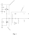
- An existing current to voltage converting module i.e. an I-V converting module, as shown in Fig. 1 , consists of a regular I-V transforming circuit 1, a sampling and holding circuit 2, and a current output sensor 3.
- the sampling and holding circuit 2 counteracts a direct current component output by the current output sensor 3 to enlarge an output dynamic range of the I-V converting module.
- a setup speed of the existing sampling and holding circuit 2 is relatively slow. This decreases a speed of the entire I-V conversion, in other words, this results in a longer time for obtaining an alternating current signal.
- a current output by the current output sensor 3 is I 0
- the direct current component output by the current output sensor 3 is I
- a switch S 2 is closed.
- the time constant is ⁇ ⁇ 100 ⁇ s.
- the setup speed of the sampling and holding circuit 2 is very low, and consequently the I-V transforming circuit 1 needs a long time to collect an alternating current component output by the current output sensor 3 and the converting rate of the I-V converting module may be severely decreased.
- Some embodiments of the present disclosure aim to provide an I-V converting module, to greatly accelerate a setup speed of a sampling and holding circuit, thereby increasing the converting rate of the I-V transforming circuit.
- some embodiments of the present disclosure provide an I-V converting module according to claim 1.
- some embodiments of the present disclosure provide an I-V converting module.
- a sampling setup stage a feedback loop formed by the N-type field-effect transistor, the I-V transforming circuit and the loop switch, is conducted, and the N-type field-effect transistor separates the sampling and holding circuit from the current output sensor, so that a time constant formed by the sampling and holding circuit and the current output sensor greatly decreases, the setup speed of the sampling and holding circuit is greatly accelerated, and the converting rate of the I-V converting module is increased.
- a voltage of an output end of the current output sensor in the sampling setup stage maintains to be unchanged, which ensures that an output current does not to change with a voltage of the output end, and which ensures the consistency of the magnitude of an output current of the current output sensor.
- the I-V converting module further includes a loop capacitor.
- the loop capacitor is connected between the gate of the N-type field-effect transistor and the input end of the I-V transforming circuit or the loop capacitor is connected between the base of the NPN- type triode and the input end of the I-V transforming circuit to improve the stability of the feedback loop.
- the bypass circuit includes a bypass switch and a power supply, and the bypass switch is connected between the gate of the N-type field-effect transistor and the power supply, wherein the bypass circuit is disabled when the bypass switch is disconnected; or the bypass circuit comprises a bypass switch and a power supply, and the bypass switch is connected between the base of the NPN- type triode and the power supply, wherein the bypass circuit is disabled when the bypass switch is disconnected.
- This embodiment provides a specific example of a bypass circuit, and this bypass circuit is relatively simple.
- the bypass circuit includes a first bypass switch, a second bypass switch, and a ground plane.
- the first bypass switch connects between the gate of the N-type field-effect transistor and the ground plane.
- the second bypass switch connects between the source and the drain of the N-type field-effect transistor.
- the bypass circuit is disabled when both of the first bypass switch and the second bypass switch are disconnected or the bypass circuit comprises a first bypass switch, a second bypass switch, and a ground plane.
- the first bypass switch is connected between the base of the NPN- type triode and the ground plane.
- the second bypass switch is connected between the emitter and the collector of the NPN- type triode. Wherein the bypass circuit is disabled when both of the first bypass switch and the second bypass switch are disconnected.
- an inverting amplifier includes an inverter or an operational amplifier. Two different types of inverting amplifiers are provided to expand an application scenario of the present disclosure.
- a transforming path includes a resistor and a switch that are connected in series, or a capacitor and a switch that are connected in series. Two different types of transforming paths are provided to ensure the feasibility of the present disclosure.
- the loop switch is an electronic switch or a physical switch. Different types of loop switches are provided to expand an application scenario of the present disclosure.
- a first embodiment of the present disclosure relates to an I-V converting module, i.e., a current to voltage converting module.
- the I-V converting module includes: an I-V transforming circuit 1, a sampling and holding circuit 2, a current output sensor 3, a source follower M 1 , a loop switch S 1 , and a bypass circuit.
- the source follower M1 includes an N-type field-effect transistor or an NPN-type triode, but without any limitation; and as an example, this embodiment is described by using the N-type field-effect transistor.
- a drain of the source follower M 1 connects to an input/output end of the sampling and holding circuit 2
- a source of the source follower connects to an input end V in of the I-V transforming circuit 1 and an output end of the current output sensor 3
- a gate of the source follower connects to an output end V out of the I-V transforming circuit 1 via the loop switch S 1
- the gate of the source follower also connects to the bypass circuit.
- the loop switch S 1 is an electronic switch or a physical switch.
- the electronic switch may be a field-effect transistor or a bipolar junction transistor. This embodiment has no limitation on the type of the loop switch S 1 .
- the current output sensor 3 includes a parasitic capacitor C 3 .
- One end of the parasitic capacitor C 3 connects to a ground terminal GND1, and the other end of the parasitic capacitor C 3 connects to an output end of the current output sensor 3.
- the output end of the current output sensor 3 connects to the source of the source follower M 1 and the input end V in of the I-V transforming circuit 1.A current Iois output by the output end of the current output sensor 3.
- a direct current component output by the current output sensor 3 is I.
- the sampling and holding circuit 2 includes: a sampling field-effect transistor M 2 , a sampling capacitor C 2 , and a sampling switch S 2 .
- One end of the sampling capacitor C 2 and a source of the sampling field-effect transistor M2 are connected to a power supply voltage VDD.
- the other end of the sampling capacitor C 2 connects to a gate of the sampling field-effect transistor M 2 and one end of the sampling switch S 2 .
- the other end of the sampling switch S 2 and a drain of the sampling field-effect transistor M 2 are connected to the drain of the source follower M 1 .
- the I-V transforming circuit 1 includes an inverting amplifier and at least one transforming path.
- the transforming path connects between an input end and an output end of the inverting amplifier.
- the input end and the output end of the inverting amplifier respectively form the input end V in and the output end V out of the I-V transforming circuit 1.
- the inverting amplifier includes an inverter or an operational amplifier (but without any limitation).
- the transforming path includes a resistor and a switch which are connected in series, or a capacitor and a switch which are connected in series. Moreover, there may be multiple or a single transforming path. The type of serial connection of the transforming path and the number of the transforming paths may be specifically set according to actual situations in this embodiment, and this is not limited in this embodiment.
- This embodiment provides two examples of the I-V transforming circuit 1, and specific descriptions are as follows.
- the inverting amplifier is an inverter 11, and a transforming path 12 includes a capacitor C 12 and a converting switch S 12 which are connected in series. Specifically, one end of the capacitor C 12 connects to an input end V in of the inverter 11, and the other end of the capacitor C 12 connects to one end of the converting switch S 12 . The other end of the converting switchS12 connects to an output end V out of the inverter 11. The input end V in and the output end V out of the inverter 11 respectively form the input end V in and the output end V out of the I-V transforming circuit 1.
- the I-V transforming circuit 1 In the I-V transforming circuit of the first type, when the converting switch S 12 is disconnected, the transforming path 12 does not work. In this situation, the I-V transforming circuit 1 is equivalent to an open-loop amplifier. When the converting switch S 12 is closed, the I-V transforming circuit 1 converts an input current signal I in into a voltage signal and outputs the voltage signal. The converting switch S 12 is controlled by a clock signal ⁇ to disconnect and close at intervals. The input current signal I in is an alternating current component output by the current output sensor 3.
- the inverting amplifier is an operational amplifier 13, and the transforming path 12 includes a resistor R 12 and a converting switch S 12 which are connected in series.
- the resistor R 12 connects to an input end Vin of the operational amplifier 13, that is, an inverting input end of the operational amplifier 13.An in-phase input end of the operational amplifier 13 receives a common-mode power supply V cm .
- the other end of the resistor R12 connects to an end of the converting switch S 12 .
- the other end of the converting switch S12 connects to an output end V out of the operational amplifier 13.
- the input end Vin and the output end V out of the operational amplifier 13 respectively form the input end V in and the output end V out of the I-V transforming circuit 1.
- the I-V transforming circuit 1 of the second type when the converting switch S 12 is disconnected, the transforming path 12 does not work. In this situation, the I-V transforming circuit 1 is equivalent to an open-loop amplifier. When the converting switch S 12 is closed, the I-V transforming circuit 1 converts an input current signal I in into a voltage signal and outputs the voltage signal.
- the I-V transforming circuit 1 may be connected by an operational amplifier and a transforming path including a capacitor and a switch which are connected in series, or may be connected by an inverter and a transforming path including a resistance and a switch which are connected in series.
- the bypass circuit may include a bypass switch S 3 and a power supply.
- the bypass switch S 3 connects between a gate of the source follower M1 and the power supply.
- the power supply of the bypass circuit may be the power supply voltage VDD of the sampling and holding circuit 2, or may be an individual power supply. This is not limited in this embodiment.
- the bypass circuit In the bypass circuit, the bypass circuit is disabled when the bypass switch S 3 is disconnected, that is, the bypass circuit is in a non-working state.
- the bypass circuit is enabled when the bypass switch S 3 is closed, that is, the bypass circuit is in a working state.
- the gate of the source follower M 1 connects to the power supply, the source follower M 1 enters into a linear region, and the source follower M 1 is equivalent to a closed switch.
- the loop switch S 1 when a control signal sh is at a high level, the loop switch S 1 is closed and the bypass circuit is disabled, that is, the bypass switch S 3 is disconnected.
- the loop switch S 1 is disconnected and the bypass circuit is enabled, that is, the bypass switch S 3 is closed, the feedback loop is bypassed, and the I-V converting module enters into an I-V converting stage.
- the loop switch S 1 and the sampling switch S 2 are controlled by the control signal sh, and the converting switch S 12 is controlled by a control signal s h.
- the control signal sh is at a high level
- the loop switch S 1 and the sampling switch S 2 are closed, and the converting switch S 12 and the bypass switch S 3 are disconnected.
- the feedback loop is conducted, the source follower M 1 enters into a saturation region and separates the sampling and holding circuit 2 from the current output sensor 3.
- the I-V converting module enters into a sampling setup stage, that is, the sampling and holding circuit 2 begins to sample a current, the gate and the drain of the sampling field-effect transistor M 2 are short-circuited, and charges the sampling capacitor C 2 , and finally a voltage V c2 in one end of the sampling capacitor C 2 stabilizes to a voltage value, making a drain current of the sampling field-effect transistor M 2 be equal to the direct current component I output by the current output sensor 3.
- the sampling field-effect transistor M 2 is equivalent to a resistor having a resistance of gm, and the resistor, the sampling capacitor C 2 , and a capacitor seen from the drain of the source follower M 1 are connected in parallel to generate a time constant ⁇ 1.
- the loop switch S 1 and the sampling switch S 2 are disconnected, and the converting switch S12 and the bypass switch S 3 is closed.
- the I-V converting module enters into an I-V converting stage, the sampling field-effect transistor M 2 outputs a constant current and counteracts the direct current component I.
- the source follower M 1 enters into the linear region. In this situation, the source follower M 1 is equivalent to a closed switch, the I-V transforming circuit converts an alternating-current signal output by the current output sensor 3 into a voltage output signal.
- the sampling setup stage that is, when the control signal sh is at a high level, the switch S 2 is closed, and a voltage of a plate of the parasitic capacitor C 3 connected to the sampling capacitor C 2 begins to be established.
- the sampling field-effect transistor M 2 is equivalent to a resistor having a resistance of gm.
- the time constant ⁇ 1 C 2 /gm1, where gm1 is a transconductance of the sampling field-effect transistor M 2 .
- the time constant of the sampling and holding circuit 2 is ⁇ ⁇ 1 ⁇ s, that is, compared with an existing sampling and holding circuit, the setup speed of the sampling and holding circuit 2 is almost increased by 100 times (usually is increased by 10 to 100 times). Therefore, the I-V transforming circuit 1 only needs a very short time to convert the alternating current component output by the current output sensor 3.
- Req is an equivalent impedance of an input end Vin in a loop including the transforming path 12 and the inverter 11.
- Req 1/(gm 2 ⁇ A)
- gm 2 is a transconductance of the source follower M1
- the setup speed of the input end V in may be greatly increased by approximately 10 to 100 times.
- this embodiment provides an I-V converting module
- the feedback loop is formed by the source follower M1, the I-V transforming circuit 1, and the loop switch S1, enabling the source follower M1 to be in the saturation region in the sampling setup stage, so as to separate the parasitic capacitor C 3 from the sampling capacitor C 1 , that is, to separate the sampling and holding circuit 2 from the current output sensor 3.
- a time constant formed by the parasitic capacitor C 3 and the sampling capacitor C 1 is greatly decreased, thereby greatly accelerating the setup speed of the sampling and holding circuit 2, and increasing the converting rate of the I-V transforming circuit.
- a control circuit of the I-V converting module provided by the present invention is relatively simple, and the formed feedback loop reuses the inverting amplifier in the I-V transforming circuit, which reduces the circuit costs.
- a second embodiment of the present invention relates to an I-V converting module. Improvements are made in the second embodiment based on the first embodiment, and the main improvement is: in the second embodiment of the present invention, as shown in Fig. 5 , a loop capacitor C 1 is added in the feedback loop.
- the loop capacitor C 1 connects between the gate of the source follower M 1 and the input end V in of the I-V transforming circuit 1.
- the loop capacitor C 1 is in parallel connection with the inverter 11. Due to the Miller effect, the loop capacitor C 1 is doubled to the source of the source follower M 1 . Therefore, the source of the source follower M 1 generates a low-frequency pole to make the feedback loop more stable.
- Req 1/(gm 2 ⁇ A)
- gm 2 is a transconductance of the source follower M1
- the setup speed of the input end V in is greatly increased.
- this embodiment adds the loop capacitor C 1 in the feedback loop, thereby improving the stability of the feedback loop.
- a third embodiment of the present invention relates to an I-V converting module.
- the third embodiment is substantially similar to the second embodiment, and the main difference is: in the second embodiment, the bypass circuit includes the bypass switch and the power supply. However, in the third embodiment of the present invention, as shown in Fig. 6 , the bypass circuit includes a first bypass switch S 3 (that is, the bypass switch S 3 in the second embodiment), a second bypass switch S 4 , and a ground plane GND2.
- the first bypass switch S 3 connects between the gate of the source follower M 1 and the ground plane GND2; and the second bypass switch S4 connects between the source and the drain of the source follower M 1 .
- the second bypass switch S 4 uses a P-type field-effect transistor, but without any limitation on the type of transistor.
- bypass circuit when both of the first bypass switch S 3 and the second bypass switch S 4 are disconnected, the bypass circuit is disabled, that is, the bypass circuit is in a non-working state.
- the bypass circuit is enabled, that is, the bypass circuit is in a working state.
- a loop switch S1 when a control signal sh is at a high level, a loop switch S1 is closed, and the first bypass switch S 3 and the second bypass switch S4 are disconnected.
- the source follower M1 enters into the saturation region (due to a negative feedback).
- sh is at a low level, the loop switch S 1 is disconnected, and both of the first bypass switch S 3 and the second bypass switch S 4 are closed, and the feedback loop is bypassed.
- the I-V transforming circuit is equivalent to a regular transforming circuit, the gate of the source follower M 1 connects to the ground plane GND2, and the source follower M1 enters into a cutoff region.
- the second bypass switch S 4 is closed, and the source follower M 1 is short-circuited.
- the mechanism of the bypass circuit in this embodiment is different.
- the gate of the source follower M 1 is pulled to a terminal of the power supply.
- the bypass circuit may introduce the ripple of the voltage to the I-V transforming circuit 1, that is, a large amount of noise may be introduced, resulting in impact on a final signal-to-noise ratio.
- the gate of the second bypass switch S 4 (when being a P-type field-effect transistor) is grounded and is conducted the short-circuited source follower M 1 , and the gate of the source follower M 1 connects the ground plane GND2 (that is, is grounded), avoiding introducing the ripple of the power supply to the I-V transforming circuit, so as to increase the signal-to-noise ratio of the I-V transforming circuit 1, that is, to improve the power supply rejection capability of the I-V transforming circuit.
- the source follower when the source follower is in the linear region in the sampling setup stage, the source follower is equivalent to a closed switch, such that some switches in the circuit are reduced, and the costs as well, and the control complexity of the I-V converting module is decreased.
- modules involved in this embodiment are all logical modules.
- a logical unit may be a physical unit, or may be part of a physical unit, or may be implemented as a combination of multiple physical units.
- units without very close relationship with the solving of the technical problems in the present invention are not introduced in this embodiment, which does not indicate that other units are not included in this embodiment.
Landscapes
- Engineering & Computer Science (AREA)
- Physics & Mathematics (AREA)
- Microelectronics & Electronic Packaging (AREA)
- Electromagnetism (AREA)
- General Physics & Mathematics (AREA)
- Radar, Positioning & Navigation (AREA)
- Automation & Control Theory (AREA)
- Nonlinear Science (AREA)
- Power Engineering (AREA)
- Amplifiers (AREA)
- Analogue/Digital Conversion (AREA)
Claims (7)
- I-V-Wandlermodul, umfassend: einen Stromausgangssensor (3), eine I-V-Transformationsschaltung (1), eine Abtast- und Halteschaltung (2), einen Quellfolger, einen Schleifenschalter (S1) und eine Umgehungsschaltung;
wobei ein erster Anschluss des Quellfolgers (M1) mit einem Eingangs-/Ausgangsende der Abtast- und Halteschaltung (2) verbunden ist, ein zweiter Anschluss des Quellfolgers (M1) mit einem Eingangsende der I-V-Transformationsschaltung (1) und einem Ausgangsende des Stromausgangssensors (3) verbunden ist und ein dritter Anschluss des Quellfolgers (M1) mit einem Ausgangsende der I-V-Transformationsschaltung (1) über den Schleifenschalter (S1) verbunden ist; und
wobei der zweite Anschluss des Quellfolgers (M1) elektrisch mit der Umgehungsschaltung verbunden ist;
wobei, wenn der Schleifenschalter (S1) geschlossen ist und die Umgehungsschaltung deaktiviert ist, eine Rückkopplungsschleife von dem Quellfolger (M1) gebildet wird, die I-V-Transformationsschaltung (1) und der Schleifenschalter (S1) geleitet werden und der Quellfolger (M1) in den Sättigungsbereich eintritt und das I-V-Wandlermodul in eine Abtasteinrichtungsphase eintritt; und
wobei, wenn der Schleifenschalter (S1) getrennt ist und die Umgehungsschaltung aktiviert ist, die Rückkopplungsschleife umgangen wird und der Quellfolger (M1) in den linearen Bereich oder Ausschaltbereich eintritt und das I-V-Wandlermodul in eine I-V-Wandlerphase eintritt; wobei der Quellfolger entweder einen Feldeffekttransistor vom n-Typ beinhaltet, bei dem der erste Anschluss seine Senke ist, der zweite Anschluss seine Quelle ist und der dritte Anschluss sein Gate ist; oder der Quellfolger eine Triode vom NPN-Typ beinhaltet, bei dem der erste Anschluss sein Kollektor ist, der zweite Anschluss sein Emitter ist und der dritte Anschluss seine Basis ist. - I-V-Wandlermodul nach Anspruch 1, wobei das I-V-Wandlermodul ferner einen Schleifenkondensator (S4) umfasst; und
wobei der Schleifenkondensator (S4) zwischen dem zweiten Anschluss des Quellfolgers und dem Eingangsende der I-V-Transformationsschaltung (1) verbunden ist. - I-V-Wandlermodul nach Anspruch 1, wobei die Umgehungsschaltung einen Umgehungsschalter (S3) und eine Stromversorgung umfasst und der Umgehungsschalter (S3) zwischen dem zweiten Anschluss des Quellfolgers und der Stromversorgung verbunden ist; und
wobei die Umgehungsschaltung deaktiviert ist, wenn der Umgehungsschalter (S3) getrennt ist. - I-V-Wandlermodul nach Anspruch 1, wobei die Umgehungsschaltung einen ersten Umgehungsschalter (S3), einen zweiten Umgehungsschalter (S4) und eine Masseebene umfasst,
wobei der erste Umgehungsschalter (S3) zwischen dem zweiten Anschluss des Quellfolgers und der Masseebene verbunden ist;
wobei der zweite Umgehungsschalter (S4) zwischen dem ersten und dritten Anschluss des Quellfolgers verbunden ist; und
wobei die Umgehungsschaltung deaktiviert ist, wenn beide des ersten Umgehungsschalters (S3) und des zweiten Umgehungsschalters (S4) getrennt sind. - I-V-Wandlermodul nach Anspruch 1, wobei die I-V-Transformationsschaltung (1) einen invertierenden Verstärker und mindestens einen Transformationspfad (12) umfasst;
wobei der Transformationspfad (12) zwischen einem Eingangsende des invertierenden Verstärkers und einem Ausgangsende des invertierenden Verstärkers verbunden ist; und
wobei das Eingangsende des invertierenden Verstärkers und das Ausgangsende des invertierenden Verstärkers das Eingangsende bzw. das Ausgangsende der I-V-Transformationsschaltung (1) bilden. - I-V-Wandlermodul nach Anspruch 5, wobei der invertierende Verstärker einen Wechselrichter (11) oder einen Betriebsverstärker (13) umfasst.
- I-V-Wandlermodul nach Anspruch 5, wobei der Transformationspfad (12) einen Widerstand (R12) und einen Schalter (S12), die in Reihe verbunden sind, oder einen Kondensator (C12) und einen Schalter (S12), die in Reihe verbunden sind, umfasst.
Applications Claiming Priority (1)
| Application Number | Priority Date | Filing Date | Title |
|---|---|---|---|
| PCT/CN2016/095429 WO2018032309A1 (zh) | 2016-08-16 | 2016-08-16 | I-v转换模块 |
Publications (3)
| Publication Number | Publication Date |
|---|---|
| EP3309645A1 EP3309645A1 (de) | 2018-04-18 |
| EP3309645A4 EP3309645A4 (de) | 2018-08-08 |
| EP3309645B1 true EP3309645B1 (de) | 2019-11-20 |
Family
ID=58285387
Family Applications (1)
| Application Number | Title | Priority Date | Filing Date |
|---|---|---|---|
| EP16898874.9A Active EP3309645B1 (de) | 2016-08-16 | 2016-08-16 | Modul zur i-v-umwandlung |
Country Status (5)
| Country | Link |
|---|---|
| US (1) | US10146245B2 (de) |
| EP (1) | EP3309645B1 (de) |
| KR (1) | KR102001754B1 (de) |
| CN (1) | CN106489107B (de) |
| WO (1) | WO2018032309A1 (de) |
Families Citing this family (1)
| Publication number | Priority date | Publication date | Assignee | Title |
|---|---|---|---|---|
| CN111402829B (zh) | 2020-04-10 | 2021-07-27 | 苏州华星光电技术有限公司 | Goa电路、显示面板 |
Family Cites Families (13)
| Publication number | Priority date | Publication date | Assignee | Title |
|---|---|---|---|---|
| US4210872A (en) * | 1978-09-08 | 1980-07-01 | American Microsystems, Inc. | High pass switched capacitor filter section |
| JPH09148852A (ja) * | 1995-11-24 | 1997-06-06 | Matsushita Electric Ind Co Ltd | 送信出力可変装置 |
| GB2384100B (en) | 2002-01-09 | 2005-10-26 | Seiko Epson Corp | An electronic circuit for controlling the current supply to an element |
| JP4252485B2 (ja) * | 2004-03-29 | 2009-04-08 | 富士通マイクロエレクトロニクス株式会社 | スイッチングレギュレータ制御回路、スイッチングレギュレータ、およびスイッチングレギュレータ制御方法 |
| EP2075909A3 (de) * | 2007-12-26 | 2016-10-12 | TPO Displays Corp. | Stromabtastverfahren und -schaltung |
| KR101547225B1 (ko) | 2007-12-26 | 2015-08-26 | 티피오 디스플레이스 코포레이션 | 전류 샘플링 방법 및 회로 |
| JP2009251877A (ja) * | 2008-04-04 | 2009-10-29 | Nec Electronics Corp | 基準電圧回路 |
| JP5161754B2 (ja) | 2008-12-19 | 2013-03-13 | パナソニック株式会社 | 煙感知器 |
| EP2734839B1 (de) | 2011-07-20 | 2017-11-08 | The Regents of The University of California | Ausbalancierter patch-clamp-verstärker zur polynukleotid-nanoporen-sequenzierung |
| CN202331254U (zh) * | 2011-09-28 | 2012-07-11 | 魏德米勒电联接国际贸易(上海)有限公司 | 设有过流保护电路模块的电流-电压转换电路 |
| CN104536510B (zh) * | 2014-11-18 | 2016-04-20 | 中山大学 | 一种差分电压转电流电路 |
| CN104614568A (zh) * | 2014-12-04 | 2015-05-13 | 深圳市德赛微电子技术有限公司 | 一种带驱动功能的电流电压转换器 |
| CN204595666U (zh) * | 2015-02-15 | 2015-08-26 | 格科微电子(上海)有限公司 | 电流源及其阵列、读出电路及放大电路 |
-
2016
- 2016-08-16 CN CN201680000904.1A patent/CN106489107B/zh active Active
- 2016-08-16 EP EP16898874.9A patent/EP3309645B1/de active Active
- 2016-08-16 KR KR1020177030105A patent/KR102001754B1/ko active Active
- 2016-08-16 WO PCT/CN2016/095429 patent/WO2018032309A1/zh not_active Ceased
-
2017
- 2017-10-25 US US15/793,563 patent/US10146245B2/en active Active
Non-Patent Citations (1)
| Title |
|---|
| None * |
Also Published As
| Publication number | Publication date |
|---|---|
| KR102001754B1 (ko) | 2019-07-18 |
| US10146245B2 (en) | 2018-12-04 |
| EP3309645A4 (de) | 2018-08-08 |
| CN106489107A (zh) | 2017-03-08 |
| KR20180037135A (ko) | 2018-04-11 |
| US20180052480A1 (en) | 2018-02-22 |
| WO2018032309A1 (zh) | 2018-02-22 |
| CN106489107B (zh) | 2018-02-13 |
| EP3309645A1 (de) | 2018-04-18 |
Similar Documents
| Publication | Publication Date | Title |
|---|---|---|
| US9634685B2 (en) | Telescopic amplifier with improved common mode settling | |
| US9407221B2 (en) | Differential amplifier circuit | |
| US10084412B2 (en) | Charge-steering amplifier circuit and control method thereof | |
| US10171052B2 (en) | Operational amplifier and differential amplifying circuit thereof | |
| US10230361B2 (en) | High-speed clocked comparators | |
| CN103840775B (zh) | 一种片上实现直流失调消除功能的限幅放大器 | |
| JP2017184122A (ja) | 差動増幅器 | |
| US20170179940A1 (en) | Track and hold circuit | |
| EP3309645B1 (de) | Modul zur i-v-umwandlung | |
| JP2007243510A (ja) | 光信号受信回路およびそれを用いた光信号受信装置 | |
| CN106385246A (zh) | 电压比较器 | |
| US11431302B2 (en) | Isolation circuit | |
| EP3675358B1 (de) | Hochgeschwindigkeitsentscheidungsvorrichtung | |
| US10607711B2 (en) | Current sample-and-hold circuit and sensor | |
| US20190166566A1 (en) | Amplifier circuit having controllable output stage | |
| US11936354B2 (en) | Amplifier circuit | |
| CN109714031B (zh) | 一种轨到轨高性能比较器 | |
| US10171040B1 (en) | Trans-impedance amplifier | |
| TW201644188A (zh) | 具單端輸入之平衡差動轉阻抗放大器及平衡方法 | |
| CN111835293A (zh) | 多跨阻恒定带宽超低噪声tia | |
| US20200067462A1 (en) | High frequency amplifier | |
| US20170272061A1 (en) | Voltage clamping circuit | |
| CN104104339B (zh) | 一种高增益宽动态范围cmos跨阻放大器 | |
| CN113037236A (zh) | 一种运算放大器 | |
| JPS59147517A (ja) | 振幅制限回路 |
Legal Events
| Date | Code | Title | Description |
|---|---|---|---|
| STAA | Information on the status of an ep patent application or granted ep patent |
Free format text: STATUS: UNKNOWN |
|
| STAA | Information on the status of an ep patent application or granted ep patent |
Free format text: STATUS: THE INTERNATIONAL PUBLICATION HAS BEEN MADE |
|
| PUAI | Public reference made under article 153(3) epc to a published international application that has entered the european phase |
Free format text: ORIGINAL CODE: 0009012 |
|
| STAA | Information on the status of an ep patent application or granted ep patent |
Free format text: STATUS: REQUEST FOR EXAMINATION WAS MADE |
|
| 17P | Request for examination filed |
Effective date: 20171025 |
|
| AK | Designated contracting states |
Kind code of ref document: A1 Designated state(s): AL AT BE BG CH CY CZ DE DK EE ES FI FR GB GR HR HU IE IS IT LI LT LU LV MC MK MT NL NO PL PT RO RS SE SI SK SM TR |
|
| AX | Request for extension of the european patent |
Extension state: BA ME |
|
| REG | Reference to a national code |
Ref country code: DE Ref legal event code: R079 Ref document number: 602016024902 Country of ref document: DE Free format text: PREVIOUS MAIN CLASS: G05F0001120000 Ipc: G11C0027020000 |
|
| A4 | Supplementary search report drawn up and despatched |
Effective date: 20180706 |
|
| RIC1 | Information provided on ipc code assigned before grant |
Ipc: G05F 3/26 20060101ALI20180702BHEP Ipc: G11C 27/02 20060101AFI20180702BHEP |
|
| GRAP | Despatch of communication of intention to grant a patent |
Free format text: ORIGINAL CODE: EPIDOSNIGR1 |
|
| STAA | Information on the status of an ep patent application or granted ep patent |
Free format text: STATUS: GRANT OF PATENT IS INTENDED |
|
| DAV | Request for validation of the european patent (deleted) | ||
| DAX | Request for extension of the european patent (deleted) | ||
| INTG | Intention to grant announced |
Effective date: 20190607 |
|
| GRAS | Grant fee paid |
Free format text: ORIGINAL CODE: EPIDOSNIGR3 |
|
| GRAA | (expected) grant |
Free format text: ORIGINAL CODE: 0009210 |
|
| STAA | Information on the status of an ep patent application or granted ep patent |
Free format text: STATUS: THE PATENT HAS BEEN GRANTED |
|
| AK | Designated contracting states |
Kind code of ref document: B1 Designated state(s): AL AT BE BG CH CY CZ DE DK EE ES FI FR GB GR HR HU IE IS IT LI LT LU LV MC MK MT NL NO PL PT RO RS SE SI SK SM TR |
|
| REG | Reference to a national code |
Ref country code: GB Ref legal event code: FG4D |
|
| REG | Reference to a national code |
Ref country code: CH Ref legal event code: EP |
|
| REG | Reference to a national code |
Ref country code: DE Ref legal event code: R096 Ref document number: 602016024902 Country of ref document: DE |
|
| REG | Reference to a national code |
Ref country code: IE Ref legal event code: FG4D |
|
| REG | Reference to a national code |
Ref country code: AT Ref legal event code: REF Ref document number: 1205095 Country of ref document: AT Kind code of ref document: T Effective date: 20191215 |
|
| REG | Reference to a national code |
Ref country code: NL Ref legal event code: MP Effective date: 20191120 |
|
| REG | Reference to a national code |
Ref country code: LT Ref legal event code: MG4D |
|
| PG25 | Lapsed in a contracting state [announced via postgrant information from national office to epo] |
Ref country code: LT Free format text: LAPSE BECAUSE OF FAILURE TO SUBMIT A TRANSLATION OF THE DESCRIPTION OR TO PAY THE FEE WITHIN THE PRESCRIBED TIME-LIMIT Effective date: 20191120 Ref country code: NO Free format text: LAPSE BECAUSE OF FAILURE TO SUBMIT A TRANSLATION OF THE DESCRIPTION OR TO PAY THE FEE WITHIN THE PRESCRIBED TIME-LIMIT Effective date: 20200220 Ref country code: GR Free format text: LAPSE BECAUSE OF FAILURE TO SUBMIT A TRANSLATION OF THE DESCRIPTION OR TO PAY THE FEE WITHIN THE PRESCRIBED TIME-LIMIT Effective date: 20200221 Ref country code: FI Free format text: LAPSE BECAUSE OF FAILURE TO SUBMIT A TRANSLATION OF THE DESCRIPTION OR TO PAY THE FEE WITHIN THE PRESCRIBED TIME-LIMIT Effective date: 20191120 Ref country code: LV Free format text: LAPSE BECAUSE OF FAILURE TO SUBMIT A TRANSLATION OF THE DESCRIPTION OR TO PAY THE FEE WITHIN THE PRESCRIBED TIME-LIMIT Effective date: 20191120 Ref country code: BG Free format text: LAPSE BECAUSE OF FAILURE TO SUBMIT A TRANSLATION OF THE DESCRIPTION OR TO PAY THE FEE WITHIN THE PRESCRIBED TIME-LIMIT Effective date: 20200220 Ref country code: SE Free format text: LAPSE BECAUSE OF FAILURE TO SUBMIT A TRANSLATION OF THE DESCRIPTION OR TO PAY THE FEE WITHIN THE PRESCRIBED TIME-LIMIT Effective date: 20191120 Ref country code: NL Free format text: LAPSE BECAUSE OF FAILURE TO SUBMIT A TRANSLATION OF THE DESCRIPTION OR TO PAY THE FEE WITHIN THE PRESCRIBED TIME-LIMIT Effective date: 20191120 |
|
| PG25 | Lapsed in a contracting state [announced via postgrant information from national office to epo] |
Ref country code: IS Free format text: LAPSE BECAUSE OF FAILURE TO SUBMIT A TRANSLATION OF THE DESCRIPTION OR TO PAY THE FEE WITHIN THE PRESCRIBED TIME-LIMIT Effective date: 20200320 Ref country code: HR Free format text: LAPSE BECAUSE OF FAILURE TO SUBMIT A TRANSLATION OF THE DESCRIPTION OR TO PAY THE FEE WITHIN THE PRESCRIBED TIME-LIMIT Effective date: 20191120 Ref country code: RS Free format text: LAPSE BECAUSE OF FAILURE TO SUBMIT A TRANSLATION OF THE DESCRIPTION OR TO PAY THE FEE WITHIN THE PRESCRIBED TIME-LIMIT Effective date: 20191120 |
|
| PG25 | Lapsed in a contracting state [announced via postgrant information from national office to epo] |
Ref country code: AL Free format text: LAPSE BECAUSE OF FAILURE TO SUBMIT A TRANSLATION OF THE DESCRIPTION OR TO PAY THE FEE WITHIN THE PRESCRIBED TIME-LIMIT Effective date: 20191120 |
|
| PG25 | Lapsed in a contracting state [announced via postgrant information from national office to epo] |
Ref country code: ES Free format text: LAPSE BECAUSE OF FAILURE TO SUBMIT A TRANSLATION OF THE DESCRIPTION OR TO PAY THE FEE WITHIN THE PRESCRIBED TIME-LIMIT Effective date: 20191120 Ref country code: RO Free format text: LAPSE BECAUSE OF FAILURE TO SUBMIT A TRANSLATION OF THE DESCRIPTION OR TO PAY THE FEE WITHIN THE PRESCRIBED TIME-LIMIT Effective date: 20191120 Ref country code: CZ Free format text: LAPSE BECAUSE OF FAILURE TO SUBMIT A TRANSLATION OF THE DESCRIPTION OR TO PAY THE FEE WITHIN THE PRESCRIBED TIME-LIMIT Effective date: 20191120 Ref country code: PT Free format text: LAPSE BECAUSE OF FAILURE TO SUBMIT A TRANSLATION OF THE DESCRIPTION OR TO PAY THE FEE WITHIN THE PRESCRIBED TIME-LIMIT Effective date: 20200412 Ref country code: EE Free format text: LAPSE BECAUSE OF FAILURE TO SUBMIT A TRANSLATION OF THE DESCRIPTION OR TO PAY THE FEE WITHIN THE PRESCRIBED TIME-LIMIT Effective date: 20191120 Ref country code: DK Free format text: LAPSE BECAUSE OF FAILURE TO SUBMIT A TRANSLATION OF THE DESCRIPTION OR TO PAY THE FEE WITHIN THE PRESCRIBED TIME-LIMIT Effective date: 20191120 |
|
| REG | Reference to a national code |
Ref country code: AT Ref legal event code: MK05 Ref document number: 1205095 Country of ref document: AT Kind code of ref document: T Effective date: 20191120 |
|
| REG | Reference to a national code |
Ref country code: DE Ref legal event code: R097 Ref document number: 602016024902 Country of ref document: DE |
|
| PG25 | Lapsed in a contracting state [announced via postgrant information from national office to epo] |
Ref country code: SM Free format text: LAPSE BECAUSE OF FAILURE TO SUBMIT A TRANSLATION OF THE DESCRIPTION OR TO PAY THE FEE WITHIN THE PRESCRIBED TIME-LIMIT Effective date: 20191120 Ref country code: SK Free format text: LAPSE BECAUSE OF FAILURE TO SUBMIT A TRANSLATION OF THE DESCRIPTION OR TO PAY THE FEE WITHIN THE PRESCRIBED TIME-LIMIT Effective date: 20191120 |
|
| PLBE | No opposition filed within time limit |
Free format text: ORIGINAL CODE: 0009261 |
|
| STAA | Information on the status of an ep patent application or granted ep patent |
Free format text: STATUS: NO OPPOSITION FILED WITHIN TIME LIMIT |
|
| 26N | No opposition filed |
Effective date: 20200821 |
|
| PG25 | Lapsed in a contracting state [announced via postgrant information from national office to epo] |
Ref country code: AT Free format text: LAPSE BECAUSE OF FAILURE TO SUBMIT A TRANSLATION OF THE DESCRIPTION OR TO PAY THE FEE WITHIN THE PRESCRIBED TIME-LIMIT Effective date: 20191120 Ref country code: SI Free format text: LAPSE BECAUSE OF FAILURE TO SUBMIT A TRANSLATION OF THE DESCRIPTION OR TO PAY THE FEE WITHIN THE PRESCRIBED TIME-LIMIT Effective date: 20191120 Ref country code: PL Free format text: LAPSE BECAUSE OF FAILURE TO SUBMIT A TRANSLATION OF THE DESCRIPTION OR TO PAY THE FEE WITHIN THE PRESCRIBED TIME-LIMIT Effective date: 20191120 |
|
| PG25 | Lapsed in a contracting state [announced via postgrant information from national office to epo] |
Ref country code: IT Free format text: LAPSE BECAUSE OF FAILURE TO SUBMIT A TRANSLATION OF THE DESCRIPTION OR TO PAY THE FEE WITHIN THE PRESCRIBED TIME-LIMIT Effective date: 20191120 |
|
| PG25 | Lapsed in a contracting state [announced via postgrant information from national office to epo] |
Ref country code: MC Free format text: LAPSE BECAUSE OF FAILURE TO SUBMIT A TRANSLATION OF THE DESCRIPTION OR TO PAY THE FEE WITHIN THE PRESCRIBED TIME-LIMIT Effective date: 20191120 |
|
| REG | Reference to a national code |
Ref country code: CH Ref legal event code: PL |
|
| PG25 | Lapsed in a contracting state [announced via postgrant information from national office to epo] |
Ref country code: CH Free format text: LAPSE BECAUSE OF NON-PAYMENT OF DUE FEES Effective date: 20200831 Ref country code: LU Free format text: LAPSE BECAUSE OF NON-PAYMENT OF DUE FEES Effective date: 20200816 Ref country code: LI Free format text: LAPSE BECAUSE OF NON-PAYMENT OF DUE FEES Effective date: 20200831 |
|
| REG | Reference to a national code |
Ref country code: BE Ref legal event code: MM Effective date: 20200831 |
|
| PG25 | Lapsed in a contracting state [announced via postgrant information from national office to epo] |
Ref country code: FR Free format text: LAPSE BECAUSE OF NON-PAYMENT OF DUE FEES Effective date: 20200831 |
|
| PG25 | Lapsed in a contracting state [announced via postgrant information from national office to epo] |
Ref country code: IE Free format text: LAPSE BECAUSE OF NON-PAYMENT OF DUE FEES Effective date: 20200816 Ref country code: BE Free format text: LAPSE BECAUSE OF NON-PAYMENT OF DUE FEES Effective date: 20200831 |
|
| PG25 | Lapsed in a contracting state [announced via postgrant information from national office to epo] |
Ref country code: TR Free format text: LAPSE BECAUSE OF FAILURE TO SUBMIT A TRANSLATION OF THE DESCRIPTION OR TO PAY THE FEE WITHIN THE PRESCRIBED TIME-LIMIT Effective date: 20191120 Ref country code: MT Free format text: LAPSE BECAUSE OF FAILURE TO SUBMIT A TRANSLATION OF THE DESCRIPTION OR TO PAY THE FEE WITHIN THE PRESCRIBED TIME-LIMIT Effective date: 20191120 Ref country code: CY Free format text: LAPSE BECAUSE OF FAILURE TO SUBMIT A TRANSLATION OF THE DESCRIPTION OR TO PAY THE FEE WITHIN THE PRESCRIBED TIME-LIMIT Effective date: 20191120 |
|
| PG25 | Lapsed in a contracting state [announced via postgrant information from national office to epo] |
Ref country code: MK Free format text: LAPSE BECAUSE OF FAILURE TO SUBMIT A TRANSLATION OF THE DESCRIPTION OR TO PAY THE FEE WITHIN THE PRESCRIBED TIME-LIMIT Effective date: 20191120 |
|
| PGFP | Annual fee paid to national office [announced via postgrant information from national office to epo] |
Ref country code: DE Payment date: 20240821 Year of fee payment: 9 |
|
| PGFP | Annual fee paid to national office [announced via postgrant information from national office to epo] |
Ref country code: GB Payment date: 20240826 Year of fee payment: 9 |