EP3306646A1 - Charged particle beam exposure apparatus and device manufacturing method - Google Patents
Charged particle beam exposure apparatus and device manufacturing method Download PDFInfo
- Publication number
- EP3306646A1 EP3306646A1 EP16807445.8A EP16807445A EP3306646A1 EP 3306646 A1 EP3306646 A1 EP 3306646A1 EP 16807445 A EP16807445 A EP 16807445A EP 3306646 A1 EP3306646 A1 EP 3306646A1
- Authority
- EP
- European Patent Office
- Prior art keywords
- charged particle
- particle beam
- exposure apparatus
- electron beam
- opening member
- Prior art date
- Legal status (The legal status is an assumption and is not a legal conclusion. Google has not performed a legal analysis and makes no representation as to the accuracy of the status listed.)
- Withdrawn
Links
Images




Classifications
-
- H—ELECTRICITY
- H01—ELECTRIC ELEMENTS
- H01J—ELECTRIC DISCHARGE TUBES OR DISCHARGE LAMPS
- H01J37/00—Discharge tubes with provision for introducing objects or material to be exposed to the discharge, e.g. for the purpose of examination or processing thereof
- H01J37/30—Electron-beam or ion-beam tubes for localised treatment of objects
- H01J37/3002—Details
- H01J37/3007—Electron or ion-optical systems
-
- G—PHYSICS
- G03—PHOTOGRAPHY; CINEMATOGRAPHY; ANALOGOUS TECHNIQUES USING WAVES OTHER THAN OPTICAL WAVES; ELECTROGRAPHY; HOLOGRAPHY
- G03F—PHOTOMECHANICAL PRODUCTION OF TEXTURED OR PATTERNED SURFACES, e.g. FOR PRINTING, FOR PROCESSING OF SEMICONDUCTOR DEVICES; MATERIALS THEREFOR; ORIGINALS THEREFOR; APPARATUS SPECIALLY ADAPTED THEREFOR
- G03F7/00—Photomechanical, e.g. photolithographic, production of textured or patterned surfaces, e.g. printing surfaces; Materials therefor, e.g. comprising photoresists; Apparatus specially adapted therefor
- G03F7/20—Exposure; Apparatus therefor
- G03F7/2051—Exposure without an original mask, e.g. using a programmed deflection of a point source, by scanning, by drawing with a light beam, using an addressed light or corpuscular source
- G03F7/2059—Exposure without an original mask, e.g. using a programmed deflection of a point source, by scanning, by drawing with a light beam, using an addressed light or corpuscular source using a scanning corpuscular radiation beam, e.g. an electron beam
-
- G—PHYSICS
- G03—PHOTOGRAPHY; CINEMATOGRAPHY; ANALOGOUS TECHNIQUES USING WAVES OTHER THAN OPTICAL WAVES; ELECTROGRAPHY; HOLOGRAPHY
- G03F—PHOTOMECHANICAL PRODUCTION OF TEXTURED OR PATTERNED SURFACES, e.g. FOR PRINTING, FOR PROCESSING OF SEMICONDUCTOR DEVICES; MATERIALS THEREFOR; ORIGINALS THEREFOR; APPARATUS SPECIALLY ADAPTED THEREFOR
- G03F1/00—Originals for photomechanical production of textured or patterned surfaces, e.g., masks, photo-masks, reticles; Mask blanks or pellicles therefor; Containers specially adapted therefor; Preparation thereof
- G03F1/20—Masks or mask blanks for imaging by charged particle beam [CPB] radiation, e.g. by electron beam; Preparation thereof
-
- G—PHYSICS
- G03—PHOTOGRAPHY; CINEMATOGRAPHY; ANALOGOUS TECHNIQUES USING WAVES OTHER THAN OPTICAL WAVES; ELECTROGRAPHY; HOLOGRAPHY
- G03F—PHOTOMECHANICAL PRODUCTION OF TEXTURED OR PATTERNED SURFACES, e.g. FOR PRINTING, FOR PROCESSING OF SEMICONDUCTOR DEVICES; MATERIALS THEREFOR; ORIGINALS THEREFOR; APPARATUS SPECIALLY ADAPTED THEREFOR
- G03F7/00—Photomechanical, e.g. photolithographic, production of textured or patterned surfaces, e.g. printing surfaces; Materials therefor, e.g. comprising photoresists; Apparatus specially adapted therefor
- G03F7/20—Exposure; Apparatus therefor
-
- G—PHYSICS
- G03—PHOTOGRAPHY; CINEMATOGRAPHY; ANALOGOUS TECHNIQUES USING WAVES OTHER THAN OPTICAL WAVES; ELECTROGRAPHY; HOLOGRAPHY
- G03F—PHOTOMECHANICAL PRODUCTION OF TEXTURED OR PATTERNED SURFACES, e.g. FOR PRINTING, FOR PROCESSING OF SEMICONDUCTOR DEVICES; MATERIALS THEREFOR; ORIGINALS THEREFOR; APPARATUS SPECIALLY ADAPTED THEREFOR
- G03F7/00—Photomechanical, e.g. photolithographic, production of textured or patterned surfaces, e.g. printing surfaces; Materials therefor, e.g. comprising photoresists; Apparatus specially adapted therefor
- G03F7/70—Microphotolithographic exposure; Apparatus therefor
- G03F7/70216—Mask projection systems
- G03F7/70233—Optical aspects of catoptric systems, i.e. comprising only reflective elements, e.g. extreme ultraviolet [EUV] projection systems
-
- G—PHYSICS
- G03—PHOTOGRAPHY; CINEMATOGRAPHY; ANALOGOUS TECHNIQUES USING WAVES OTHER THAN OPTICAL WAVES; ELECTROGRAPHY; HOLOGRAPHY
- G03F—PHOTOMECHANICAL PRODUCTION OF TEXTURED OR PATTERNED SURFACES, e.g. FOR PRINTING, FOR PROCESSING OF SEMICONDUCTOR DEVICES; MATERIALS THEREFOR; ORIGINALS THEREFOR; APPARATUS SPECIALLY ADAPTED THEREFOR
- G03F7/00—Photomechanical, e.g. photolithographic, production of textured or patterned surfaces, e.g. printing surfaces; Materials therefor, e.g. comprising photoresists; Apparatus specially adapted therefor
- G03F7/70—Microphotolithographic exposure; Apparatus therefor
- G03F7/70383—Direct write, i.e. pattern is written directly without the use of a mask by one or multiple beams
- G03F7/704—Scanned exposure beam, e.g. raster-, rotary- and vector scanning
-
- G—PHYSICS
- G03—PHOTOGRAPHY; CINEMATOGRAPHY; ANALOGOUS TECHNIQUES USING WAVES OTHER THAN OPTICAL WAVES; ELECTROGRAPHY; HOLOGRAPHY
- G03F—PHOTOMECHANICAL PRODUCTION OF TEXTURED OR PATTERNED SURFACES, e.g. FOR PRINTING, FOR PROCESSING OF SEMICONDUCTOR DEVICES; MATERIALS THEREFOR; ORIGINALS THEREFOR; APPARATUS SPECIALLY ADAPTED THEREFOR
- G03F7/00—Photomechanical, e.g. photolithographic, production of textured or patterned surfaces, e.g. printing surfaces; Materials therefor, e.g. comprising photoresists; Apparatus specially adapted therefor
- G03F7/70—Microphotolithographic exposure; Apparatus therefor
- G03F7/70691—Handling of masks or workpieces
- G03F7/70775—Position control, e.g. interferometers or encoders for determining the stage position
-
- G—PHYSICS
- G03—PHOTOGRAPHY; CINEMATOGRAPHY; ANALOGOUS TECHNIQUES USING WAVES OTHER THAN OPTICAL WAVES; ELECTROGRAPHY; HOLOGRAPHY
- G03F—PHOTOMECHANICAL PRODUCTION OF TEXTURED OR PATTERNED SURFACES, e.g. FOR PRINTING, FOR PROCESSING OF SEMICONDUCTOR DEVICES; MATERIALS THEREFOR; ORIGINALS THEREFOR; APPARATUS SPECIALLY ADAPTED THEREFOR
- G03F7/00—Photomechanical, e.g. photolithographic, production of textured or patterned surfaces, e.g. printing surfaces; Materials therefor, e.g. comprising photoresists; Apparatus specially adapted therefor
- G03F7/70—Microphotolithographic exposure; Apparatus therefor
- G03F7/708—Construction of apparatus, e.g. environment aspects, hygiene aspects or materials
- G03F7/7085—Detection arrangement, e.g. detectors of apparatus alignment possibly mounted on wafers, exposure dose, photo-cleaning flux, stray light, thermal load
-
- H—ELECTRICITY
- H01—ELECTRIC ELEMENTS
- H01J—ELECTRIC DISCHARGE TUBES OR DISCHARGE LAMPS
- H01J37/00—Discharge tubes with provision for introducing objects or material to be exposed to the discharge, e.g. for the purpose of examination or processing thereof
- H01J37/30—Electron-beam or ion-beam tubes for localised treatment of objects
- H01J37/305—Electron-beam or ion-beam tubes for localised treatment of objects for casting, melting, evaporating, or etching
-
- H—ELECTRICITY
- H10—SEMICONDUCTOR DEVICES; ELECTRIC SOLID-STATE DEVICES NOT OTHERWISE PROVIDED FOR
- H10P—GENERIC PROCESSES OR APPARATUS FOR THE MANUFACTURE OR TREATMENT OF DEVICES COVERED BY CLASS H10
- H10P72/00—Handling or holding of wafers, substrates or devices during manufacture or treatment thereof
- H10P72/50—Handling or holding of wafers, substrates or devices during manufacture or treatment thereof for positioning, orientation or alignment
-
- H—ELECTRICITY
- H10—SEMICONDUCTOR DEVICES; ELECTRIC SOLID-STATE DEVICES NOT OTHERWISE PROVIDED FOR
- H10P—GENERIC PROCESSES OR APPARATUS FOR THE MANUFACTURE OR TREATMENT OF DEVICES COVERED BY CLASS H10
- H10P72/00—Handling or holding of wafers, substrates or devices during manufacture or treatment thereof
- H10P72/70—Handling or holding of wafers, substrates or devices during manufacture or treatment thereof for supporting or gripping
- H10P72/76—Handling or holding of wafers, substrates or devices during manufacture or treatment thereof for supporting or gripping using mechanical means, e.g. clamps or pinches
- H10P72/7604—Handling or holding of wafers, substrates or devices during manufacture or treatment thereof for supporting or gripping using mechanical means, e.g. clamps or pinches the wafers being placed on a susceptor, stage or support
- H10P72/7618—Handling or holding of wafers, substrates or devices during manufacture or treatment thereof for supporting or gripping using mechanical means, e.g. clamps or pinches the wafers being placed on a susceptor, stage or support characterised by a movable susceptor, stage or support, others than those only rotating on their own vertical axis, e.g. susceptors on a rotating carrousel
-
- H—ELECTRICITY
- H10—SEMICONDUCTOR DEVICES; ELECTRIC SOLID-STATE DEVICES NOT OTHERWISE PROVIDED FOR
- H10P—GENERIC PROCESSES OR APPARATUS FOR THE MANUFACTURE OR TREATMENT OF DEVICES COVERED BY CLASS H10
- H10P76/00—Manufacture or treatment of masks on semiconductor bodies, e.g. by lithography or photolithography
-
- H—ELECTRICITY
- H10—SEMICONDUCTOR DEVICES; ELECTRIC SOLID-STATE DEVICES NOT OTHERWISE PROVIDED FOR
- H10W—GENERIC PACKAGES, INTERCONNECTIONS, CONNECTORS OR OTHER CONSTRUCTIONAL DETAILS OF DEVICES COVERED BY CLASS H10
- H10W20/00—Interconnections in chips, wafers or substrates
- H10W20/01—Manufacture or treatment
- H10W20/031—Manufacture or treatment of conductive parts of the interconnections
- H10W20/067—Manufacture or treatment of conductive parts of the interconnections by modifying the pattern of conductive parts
- H10W20/068—Manufacture or treatment of conductive parts of the interconnections by modifying the pattern of conductive parts by using a laser, e.g. laser cutting or laser direct writing
Definitions
- the present invention relates to a charged particle beam exposure apparatus and a device manufacturing method, and more particularly to a charged particle beam exposure apparatus that exposes a target with a charged particle beam, and a device manufacturing method that uses the charged particle beam exposure apparatus.
- an exposure apparatus used in a lithography process to produce electronic devices such as a semiconductor device that uses ultraviolet light from far ultraviolet region to vacuum ultraviolet region as an exposure beam (hereinafter called an ultraviolet light exposure apparatus)
- an ultraviolet light exposure apparatus in order to increase resolution, shortening exposure wavelength, optimizing illumination conditions, applying a liquid immersion method to further increase numerical aperture of a projection optical system and the like have been performed.
- a charged particle beam exposure apparatus exposing a target with a charged particle beam, comprising: a stage holding the target that can be relatively moved with respect to the charged particle beam; a charged particle beam optical system irradiating the target with the charged particle beam; and a charged particle detection device arranged at an emitting side of the charged particle beam of the charged particle beam optical system and in the periphery of the charged particle beam, to detect the charged particle beam.
- a charged particle beam exposure apparatus exposing a target with a charged particle beam, comprising: a stage, holding the target that can be relatively moved with respect to the charged particle beam; a charged particle beam optical system, irradiating the target with the charged particle beam; and an opening member arranged at an emitting side of the charged particle beam of the charged particle beam optical system, having an opening formed, through which the charged particle beam passes.
- a device manufacturing method including: exposing the substrate using the charged particle beam exposure apparatus according to one of the first and the second aspect, and developing the substrate that has been exposed.
- FIG. 1 schematically shows a structure of an electron beam exposure apparatus 100 according to the first embodiment.
- Electron beam exposure apparatus 100 is equipped with an electron beam optical system to be described later on; therefore, the description below will be made with a Z-axis being parallel to the optical axis of the electron beam optical system, and a Y-axis and an X-axis being orthogonal to each other in a plane perpendicular to the Z-axis.
- the charged particle beam is not limited to the electron beam, and may be a beam using a charged particle such as an ion beam.
- Electron beam exposure apparatus 100 is equipped with a vacuum chamber 10, and an exposure system 20 housed inside an exposure chamber 12 divided by vacuum chamber 10.
- Exposure system 20 is equipped with a stage 22 movable holding a wafer W, and an electron beam irradiation device 30 that has an electron beam optical system 32 which irradiates wafer W coated with a resist for electron beams (sensitive agent) with an electron beam.
- Stage 22 is moved with predetermined strokes in an X-axis direction and a Y-axis direction on a base member (not shown) by a stage drive system 24 (not shown in FIG. 1 , refer to FIG. 7 ) including a linear motor or the like, and is also finely moved in a Z-axis direction, a rotation direction around the X-axis ( ⁇ x direction), a rotation direction around the Y-axis ( ⁇ y direction), and a rotation direction around the Z-axis ( ⁇ z direction).
- a stage drive system 24 (not shown in FIG. 1 , refer to FIG. 7 ) including a linear motor or the like, and is also finely moved in a Z-axis direction, a rotation direction around the X-axis ( ⁇ x direction), a rotation direction around the Y-axis ( ⁇ y direction), and a rotation direction around the Z-axis ( ⁇ z direction).
- a magnetic shield is applied to the linear motor, and magnetic flux leakage from the linear motor to the wafer side is effectively suppressed or prevented.
- Electron beam irradiation device 30, as is shown in FIG. 1 has a barrel 34.
- This barrel 34 is formed in a cylindrical shape.
- Barrel 34 has an electron beam emitting section 34a, a main section 34b that houses an electron gun section and an electromagnetic lens to be described later on, and a step section (flange section) arranged in between the electron beam emitting section 34a and main section 34b.
- Barrel 34 is supported from below by a metrology frame 40 consisting of an annular plate member.
- electron beam emitting section 34a of barrel 34 is formed by a small diameter section whose diameter is smaller than main section 34b, and the small diameter section is inserted into a circular opening in metrology frame 40 so that barrel 34 is supported from below by metrology frame 40 in a state where the bottom surface of the step section is in contact with the upper surface of metrology frame 40.
- Metrology frame 40 has, to the outer periphery section, each of the lower end of three suspension support mechanisms 50a, 50b, and 50c serving as connecting members having a flexible structure (however, suspension support mechanism 50c in FIG. 1 is hidden in the depth of 50a) connected, arranged apart at a center angle of 120 degrees, and is supported in a suspended state from a top plate (ceiling wall) of vacuum chamber 10 that divides exposure chamber 12 via suspension support mechanisms 50a, 50b, and 50c. That is, in the manner described above, electron beam irradiation device 30 is supported by suspension at three points with respect to vacuum chamber 10.
- suspension support mechanisms 50a, 50b, and 50c serving as connecting members having a flexible structure (however, suspension support mechanism 50c in FIG. 1 is hidden in the depth of 50a) connected, arranged apart at a center angle of 120 degrees, and is supported in a suspended state from a top plate (ceiling wall) of vacuum chamber 10 that divides exposure chamber 12 via suspension support mechanisms 50a, 50b, and 50c
- the three suspension support mechanisms 50a, 50b, and 50c as is representatively shown in suspension support mechanism 50a in FIG. 1 , each has a passive vibration isolation pad 52 provided at the upper end of each of the suspension support mechanisms, and a wire 54 made of steel having one end connected to the lower end of vibration isolation pad (vibration isolation section) 52 and the other end connected to metrology frame 40.
- Vibration isolation pad 52 is fixed to the top plate of vacuum chamber 10, and each includes an air damper or a coil spring.
- vibration isolation pad 52 Since a large part of the vibration component in the Z-axis direction parallel to an optical axis AX of electron beam optical system 32 is absorbed by vibration isolation pad 52, high vibration isolation performance can be obtained in the direction parallel to optical axis AX of electron beam optical system 32. Also, natural frequency of suspension support mechanisms 50a, 50b, and 50c is lower in a direction perpendicular to optical axis AX than in the direction parallel to optical axis AX of electron beam optical system 32.
- the length (length of wire 54) of the three suspension support mechanisms 50a, 50b, and 50c is set long enough so that the vibration isolation performance (capacity of preventing vibration such as floor vibration transmitted from the outside to vacuum chamber 10 from traveling to electron beam irradiation device 30) in the direction perpendicular to optical axis AX becomes sufficiently high.
- the vibration isolation performance Capacity of preventing vibration such as floor vibration transmitted from the outside to vacuum chamber 10 from traveling to electron beam irradiation device 30
- relative position between electron beam irradiation device 30 and vacuum chamber 10 may change at a comparatively low frequency.
- a positioning device 14 (not shown in FIG. 1 , refer to FIG. 7 ) of a non-contact method is provided in between electron beam irradiation device 20 and vacuum chamber 10.
- This positioning device 14 can be structured including a six-axis acceleration sensor and a six-axis actuator, as is disclosed in, for example, International Publication WO 2007/077920 , and the like.
- Positioning device 14 is controlled by a controller 60 (refer to FIG. 7 ).
- Electron beam irradiation device 30 includes parts such as an electron gun section 36 partly provided inside barrel 34 that generates electrons and performs acceleration by an acceleration power supply (not shown) to form an electron beam EB (refer to FIG. 2 ), and an electron beam optical system 32 arranged in a predetermined positional relation inside barrel 34 that is structured of various electrodes and the like such as an electromagnetic lens and an aperture used to perform forming of spots of electron beam EB, adjustment of irradiation position of electron beam EB with respect to wafer W, adjustment of irradiation amount and the like.
- Electromagnetic lens includes an electromagnetic lens that has a focus coil (hereinafter referred to as a focus lens for convenience), an electromagnetic lens that has a deflection coil (hereinafter referred to as a deflection lens for convenience) and the like.
- FIG. 1 representatively shows a focus lens 32a and deflection lens 32b that structure electron beam optical system 32.
- focus lens 32a is controlled by controller 60 via a focus control section 64
- deflection lens 32b is controlled by controller 60 via an electron beam deflection control section 66.
- electron beam optical system 32 consists of a multi-beam optical system that can be separately turned on/off and can irradiate n (n is, for example, 500) deflectable beams.
- n is, for example, 500
- the multi-beam optical system a system can be used that has a structure similar to the optical system disclosed in, for example, Japanese Unexamined Patent Application Publication No. 2011-258842 , International Publication WO 2007/017255 , and the like.
- circular spots of the electron beams are formed simultaneously at 500 points set at an equal spacing within, for example, a 10 ⁇ m ⁇ 20 nm exposure area (a slit shaped area extending in the X direction). That is, one exposure area is formed with 500 electron beams.
- the circular spot of the electron beam is formed having a diameter (e.g. a diameter of 20 nm) smaller than the resolution limit of the ultraviolet light exposure apparatus.
- a predetermined direction e.g. Y-axis direction
- the pattern is formed on the shot areas on the wafer.
- Electron beam irradiation device 30 is equipped with a reflected electron detection device to be described later on that detects reflected electrons. Electron beam irradiation device 30 is controlled by controller60 (refer to FIG. 7 ).
- Controller 60 can deflect and scan electron beam EB by controlling deflection lens 32b.
- the range that electron beam EB can be scanned by deflection lens 32b can be decided by the deflectability of deflection lens 32b.
- the scanning range of electron beam EB can be set smaller than at least the radius of barrel 34.
- an opening member 16 is arranged on a -Z side of electron beam irradiation device 30 (electron beam optical system 32) and also on the +Z side of wafer W held by stage 22 in the Z-axis direction, that is, on the electron beam emitting side of electron beam irradiation device30. Opening member 16 is arranged, for example, parallel to an XY plane, which is a surface intersecting the optical axis of electron beam optical system 32, and is supported in a suspended state from metrology frame 40 via a plurality of (at least three) support members 42. Opening member 16 has strength strong enough to maintain flatness in a state supported by the plurality of support members 42.
- FIG. 2 shows an enlarged view of the lower end of barrel 34, metrology frame 40, and opening member 16 in FIG. 1 in a state partly broken, along with stage 22.
- FIGS. 3A and 3B show a perspective view of opening member 16 when viewed from above obliquely and a planar view, respectively.
- FIG. 4 shows the part of circle A in FIG. 2 of opening member 16 enlarged
- FIG. 5 shows the part of circle B in FIG. 4 enlarged.
- Opening member 16 as is shown in FIGS. 3A and 3B , consists of a plate member having a shape almost a square, and a conical recess section 16a is formed in the center. Conical recess section 16a is formed so that the size of the opening gradually becomes smaller from the upper surface (electron beam optical system 32) side of opening member 16 towards the lower surface (wafer W) side.
- a dielectric is used as the material of opening member 16.
- a dielectric material also having a low thermal expansion coefficient such as, e.g. a zero expansion ceramic, is used.
- an engraved recess section 16b of a circular cross section having, for example, a diameter D of about 100 ⁇ m to 200 ⁇ m is formed, and in the center of the bottom wall section of engraved recess section 16b, a fine rectangular slit (or a circle) shaped opening 16c is formed. Opening 16c is slightly larger than an exposure field, having a size of about 30 ⁇ m.
- a metal reflection film 18 is provided, and on the upper surface of reflection film 18, a reflection surface 18a is formed. In other words, reflection surface 18a is provided around opening 16c. Also, the upper surface of the bottom wall is provided to face electron beam optical system 32.
- a calibration pattern consisting of a line-and-space pattern whose periodic direction is in the first direction is formed, and on reflection surface 18a at both sides of opening 16c in a second direction (a direction orthogonal to the first direction, the X-axis direction in FIG. 5 ), a calibration pattern CP (in FIG.
- Y calibration pattern CP whose periodic direction is on the Y-axis direction is shown
- Calibration pattern CP each has different reflectance in the line section and the space section.
- calibration pattern CP shown is made much thicker than the actual size of thickness for convenience of explanation.
- Thickness t of the bottom wall (including the thickness of reflection film 18) of engraved recess section 16b on which reflection film 18 and calibration pattern CP are formed is desirably as thin as possible.
- the thickness of the bottom wall of engraved recess section 16 is set, as an example, to about 10 ⁇ m to 50 ⁇ m.
- reflection surface 18a is a plane parallel to the XY plane, the embodiment is not limited to this, and may be a curved surface that has an arc shape in a side view whose center is on the optical axis of electron beam optical system 32, or may be an inclined surface corresponding thereto. Also, reflection surface 18a may be formed separated in the first direction (Y-axis direction) and the second direction (X-axis direction).
- a plurality of reflected electron detection devices 38 is provided near the lower end of deflection lens 32b of electron beam optical system 32.
- the plurality of reflected electron detection devices 38 is arranged on the emitting side of deflection lens 32b and also at the periphery of charged particle beams.
- the periphery of charged particle beams refers to the range in which electron beams EB can be scanned by deflection lens 32b as is previously described.
- Each of the plurality of reflected electron detection devices 38 is structured, for example, by a semiconductor detector, and sends detection signals corresponding to reflected electrons which are detected to a signal processor 62 (refer to FIG. 7 ).
- Signal processor 62 after amplifying the detection signals of the plurality of reflected electron detection devices 38 with an amplifier (not shown), performs signal processing and sends the processing results to controller 60 (refer to FIG. 7 ).
- Each of the plurality of reflected electron detection devices 38 is provided at a position where reflected electrons generated at an alignment mark AM that enters barrel 34 via opening 16c and the inner space of engraved recess section 16b can be detected when alignment mark AM on wafer W is irradiated with electron beam EB via the inner space of engraved recess section 16b and opening 16c of opening member 16.
- Alignment mark AM formed on wafer W is formed by a two-dimensional mark including a line-and-space pattern whose periodic direction is in the Y-axis direction (the first direction) and a line-and-space pattern whose periodic direction is in the X-axis direction (the second direction).
- reflected electron detection devices 38 y1 and 38 y2 that detects reflected electrons generated in a direction tilted with respect to the optical axis within a YZ plane from alignment mark AM on wafer W
- a pair of reflected electron detection devices 38 x1 and 38 x2 that detects reflected electrons generated in a direction tilted with respect to the optical axis within an XZ plane from alignment mark AM is also actually provided (refer to FIG. 7 ).
- reflected electron detection devices 38 x1 , 38 x2 , 38 y1 , and 38 y2 are also used when performing calibration of beam position to be described later on.
- Position information of stage 22 is measured by an encoder system 28 (refer to FIG. 7 ).
- Encoder system 28 as is shown in FIG. 2 , is formed in an area excluding a section at the rear surface side of recess section16a at the lower surface (surface on the -Z side) of opening member 16, and consists of a grating RG consisting of a reflection type two-dimensional grating whose periodic directions are in the X-axis direction and the Y-axis direction and four heads 26 (hereinafter described as heads 26 1 to 26 4 for convenience) with one head arranged at one corner of the four corners of stage 22 facing grating RG.
- a reflective diffraction grating having a pitch of, e.g. 1 ⁇ m, for each of the periodic directions is used.
- grating RG a grating structured of four sections that can individually face the four heads 26 may be used, as is disclosed in, for example, U.S. Patent Application Publication No. 2011/0053061 .
- heads 26 1 and 26 3 are provided whose measurement directions are in the X-axis direction and the Z-axis direction
- heads 26 2 and 26 4 are provided whose measurement directions are in the Y-axis direction and the Z-axis direction.
- the four heads 26 1 to 26 4 are arranged at each of the vertex positions of the same square or rectangle in a planar view.
- FIG. 2 shows only two heads 26 1 and 26 2 of the four heads.
- Heads 26 1 and 26 3 make up two-axis linear encoders 28 1 and 28 3 , respectively, which irradiate grating RG with a beam and measure position information of stage 22 in the X-axis direction and the Z-axis direction. Also, heads 26 2 and 26 4 make up two-axis linear encoders 28 2 and 28 4 , respectively, which irradiate grating RG with a beam and measure position information of stage 22 in the Y-axis direction and the Z-axis direction.
- an encoder head having a structure similar to a displacement measurement sensor head disclosed in, for example, U.S. Patent No. 7,561,280 can be used.
- controller 60 can measure the position of stage 22 (wafer W) in directions of six degrees of freedom (in each of the X-axis, the Y-axis, the Z-axis, the ⁇ x, the ⁇ y, and the ⁇ z directions), based on the information measured by encoder system 28.
- FIG. 7 is a block diagram showing an input-output relation of controller 60 which structures a control system of electron beam exposure apparatus 100.
- Controller 60 includes a microcomputer and the like, and has overall control over each section of electron beam exposure apparatus 100 including the sections shown in FIG. 7 .
- controller 60 controls electron beam EB emitted from electron beam optical system 32 and stage 22 according to a predetermined pattern data and each drawing parameter decided in advance, and performs exposure (pattern drawing) with respect to wafer W.
- a plurality of layers of patterns has to be overlaid and formed on a wafer, which makes overlay between an underlayer pattern and a pattern to be drawn important.
- controller 60 controlling deflection lens 32b via electron beam deflection control section 66, electron beam EB is sequentially scanned with respect to two or more alignment marks AM (refer to FIG. 6 ) formed in advance on the wafer, and on this scanning, reflected electrons generated from alignment marks AM are detected by reflected electron detection device 38.
- accelerating voltage of electron beam EB is set to the same accelerating voltage as the time of exposure (the time of pattern drawing).
- FIG. 6 shows reflected electrons RE of electron beam EB irradiated on alignment marks AM along an optical path (an optical path indicated by a solid line in the drawing) parallel to the optical axis, moving toward reflected electron detection devices 38 y1 and 38 y2 from alignment marks AM.
- Controller 60 specifies the position of alignment marks AM based on deflection information (information including deflection angle, deflection direction and the like) of the electron beam obtained from electron beam deflection control section 66 and processing results of detection signals of the marks obtained from signal processor 62, and based on the position and stage coordinate information obtained from encoder system 28 at the time of detection, acquires the position of alignment marks AM on a stage coordinate system.
- deflection information information including deflection angle, deflection direction and the like
- target position information for positioning the shot areas on the wafer to an exposure position (irradiation position in a reference state of the electron beam, that is, irradiation position of electron beam EB on wafer W when electron beam EB is irradiated along the optical path indicated by the solid line in FIG. 6 on optical axis AX) can be acquired.
- controller 60 draws the pattern while moving the wafer (stage 22) at the time of exposure of the wafer (at the time of pattern drawing with respect to the wafer).
- alignment marks AM as a reference as is described, the pattern can be drawn at a desired position at all times, and a new pattern to be drawn can be overlaid favorably on the pattern which has already been formed on wafer W.
- controller 60 performs initial setting for calibration of drift (position and focus) of electron beam EB at the time of alignment measurement before starting exposure, prior to measuring mark position information of alignment marks AM.
- Controller 60 sets the position of wafer W in the Z-axis direction to the same position as the time of exposure and scans alignment marks AM while changing focal position by changing current of a focus coil that focus lens 32a described earlier has via focus control section 64, and from a change in detection signals of reflected electron detection device 38 (a predetermined one among 38 x1 , 38 x2 , 38 y1 , and 38 y2 ) that has detected reflected electron RE, the position where the change is sharpest is acquired as the optimum focal position, and the current corresponding to the optimum focal position is to be supplied thereafter to the focus coil.
- controller 60 deflects and scans electron beam EB with respect to the four calibration patterns CP on reflection surface 18a and detects reflected electrons from each of the calibration patterns CP using reflected electron detection devices 38 x1 , 38 x2 , 38 y1 , and 38 y2 , and based on deflection information of electron beam EB obtained from electron beam deflection control section 66 and information on processing results of detection signals of calibration patterns CP obtained from signal processor 62, position (hereinafter referred to as position information of calibration patterns CP) of calibration patterns CP with the position of electron beam EB in the reference state serving as a reference, that is, information on the amount of angle that electron beam EB should be deflected in each of the X direction and the Y direction from the reference state or on the direction of deflection so that the center position of each of the calibration patterns CP is made to be irradiated with electron beam EB is to be acquired.
- position information of calibration patterns CP position of calibration patterns CP
- FIG. 8 shows a state where reflected electrons RE are detected using reflected electron detection device 38 y1 when acquiring position information of calibration pattern CP on the reflection surface positioned at the +Y side of opening 16c.
- Drift includes deviation of deflection angle, shift of deflection direction, and shift with respect to optical axis AX.
- controller 60 functions as a detection device that detects the drift.
- controller 60 stores the state of change of detection signals of a predetermined one reflected electron detector that has detected reflected electrons from calibration patterns CP, such as, for example, reflected electron detection device 38 y1 , in an internal memory. This is because controller 60 detects the drift of focus of electron beam EB later on, using the state of change of detection signals as a reference. Note that all reflected electron detection devices may have the state of change of detection signals stored in the internal memory.
- controller 60 acquires the target position information to position the shot areas on the wafer at the exposure position as is previously described based on results of the alignment measurement, and at the time of exposure on the wafer (at the time of pattern drawing with respect to the wafer), draws the pattern while moving the wafer (stage 22) based on the acquired target position information.
- This wafer exposure is performed, by repeating the alternate scanning operation in which scanning exposure of the wafer is performed alternately in the +Y direction and the -Y direction and the operation (stepping operation) of moving the wafer by a distance the same as the width of the exposure area in the X-axis direction to one side of the X-axis direction during deceleration and acceleration of the wafer in the Y-axis direction between scanning in the +Y direction (plus scan) and scanning in the -Y direction (minus scan).
- the alternate scanning operation has to be repeated many times in order to expose one wafer or one exposure area, the exposure operation takes much more time than the ultraviolet light exposure apparatus and the like. Therefore, the calibration of drift (position and focus) of electron beam EB has to be performed even while exposing one wafer.
- controller 60 deflects and scans electron beam EB with respect to the four calibration patterns CP on reflection surface 18a and detects reflected electrons RE generated from each of the calibration patterns CP using reflected electron detection devices 38 x1 , 38 x2 , 38 y1 , and 38 y2 , similar to the time of initial setting for calibration previously described. Then, controller 60 acquires position information of calibration patterns CP based on deflection information of the electron beam obtained from electron beam deflection control section 66 and information on processing results of detection signals of calibration patterns CP obtained from the signal processor, and stores the information in memory.
- controller 60 calculates the position of calibration patterns CP according to a procedure decided in advance, based on position information of calibration pattern CP obtained N times (N is a natural number, e.g. 10 times). For example, an average of the remaining position information which is information excluding from the 10 times the position that has changed maximum and minimum from the time of initial setting, position information that has changed maximum from the time of initial setting, or an average of the 10 times is acquired as the position of calibration patterns CP. Then, by comparing the calculated position and the position information of calibration patterns CP at the time of initial setting described above, the controller acquires the drift amount of the position of electron beam EB. Note that instead of the average of 10 times, controller 60 may acquire the average less than 10 times of moving.
- controller 60 calibrates the drift each time the drift amount of the position of electron beam EB is acquired, or calibrates the drift only when the drift amount exceeds a threshold value.
- controller 60 acquires the state of change of detection signals of reflected electrons RE from a predetermined calibration pattern CP once in every N times, compares the acquired state of change to the corresponding state of change of the detection signals stored at the time of initial setting, and detects the drift amount of the focus of the electron beam. Then, controller 60 calibrates the drift each time the drift amount of the focus of electron beam EB is acquired by adjusting the current supplied to the focus coil, or calibrates the drift only when the drift amount exceeds a threshold value.
- the exposure apparatus since the exposure apparatus is equipped with the plate shaped opening member 16 arranged facing wafer W via a predetermined gap on the wafer W side in the optical axis AX direction (the Z-axis direction) of electron beam optical system 32, with opening 16c formed through which electron beam EB from electron beam optical system 32 passes, this can suppress an adverse effect that the electrical charge accumulated on wafer W by irradiation of electron beam EB has on the irradiation position of electron beam EB when compared to the case when the exposure apparatus is not equipped with opening member 16.
- opening member 16 is made of a dielectric (zero expansion ceramic)
- the adverse effect that the electrical charge accumulated on wafer W by irradiation of electron beam EB has on the irradiation position of electron beam EB can be suppressed more effectively.
- electron beam EB is deflected and scanned with respect to calibration patterns CP on reflection surface 18a formed on the inner bottom surface of the engraved recess section of opening member 16, and by detecting reflected electrons RE generated at calibration patterns CP with reflected electron detection device 38, the drift of position of electron beam EB is detected. Therefore, the drift of position of electron beam EB can be detected, without using the alignment marks on the wafer. Also, with electron beam exposure apparatus 100, controller 60 detects the drift of position of electron beam EB during the stepping operation (during the deceleration and acceleration period in the scanning direction) in between the plus scan and the minus scan in the exposure operation of the wafer. Therefore, it becomes possible to detect the drift of position of electron beam EB and perform calibration of the drift, without decreasing the throughput.
- electron beam exposure apparatus100 along with detecting the drift of position of electron beam EB, it is possible to detect the drift amount of focus of the electron beam, based on change of detection signals of the reflected electrons from the calibration pattern acquired for detecting the drift of position of electron beam EB, and to perform calibration of the drift of focus of electron beam EB when necessary.
- the embodiment is not limited to this, and the reference marks provided on stage 22 may be scanned with the electron beam.
- the scan becomes free of the risk of being affected by the electron beam resist coated on wafer W, being affected by defective shapes of alignment marks, and the like.
- a measurement device for measuring the positional relation between the alignment marks and the reference marks such as for example, a microscope or the like will be necessary.
- controller 60 scans electron beam EB via electron beam deflection control section 66 with respect to reflection surface 18a in a range including a border section with the opening (edge of reflection surface 18a).
- controller 60 to detect reflected electrons from reflection surface 18a using reflected electron detection devices 38 x1 , 38 x2 , 38 y1 , and 38 y2 and to detect position of the edge of reflection surface 18a with the position of electron beam EB serving as a reference, based on deflection information of electron beam EB obtained from electron beam deflection control section 66 and information on processing results of detection signals of reflection surface 18a obtained from signal processor 62, similar to the detection of position information of calibration pattern CP previously described.
- controller 60 scans electron beam EB via electron beam deflection control section 66 with respect to reflection surface18a in a range including the edge of reflection surface 18a.
- detection signals of reflected electrons from reflection surface 18a including the edge are obtained by scanning electron beam EB with respect to reflection surface 18a, it becomes possible to detect drift amount of the focus of the electron beam based on change of the detection signals, and to perform calibration of the drift of the focus of electron beam EB when necessary.
- reflection surface 18a is formed on the upper surface of the bottom wall of engraved recess section 16b of opening member 16
- a reflection pattern having a reflectance to electron beam EB different from that of the upper surface may be formed on the upper surface of the bottom wall of recess section 16b, without the reflection surface being formed.
- the same working effect can be produced as the embodiment described above.
- opening member 16 is supported by metrology frame 40 which supports barrel 34 (electron beam irradiation device 30) having electron beam optical system 32 inside
- positional relation between opening member 16 and metrology frame 4 0 may change by the influence of heat or influence of other factors. Therefore, for example, as is shown in FIG. 7 in a dotted (broken line) block, a measurement device 90 that measures the relative position between metrology frame 40 and opening member 16 may be further provided, and controller 60 may correct the position of electron beam EB based on measurement information of the measurement device.
- opening member 16 is supported by metrology frame 40 supporting barrel 34 (electron beam irradiation device 30) that has electron beam optical system 32 inside
- the embodiment is not limited to this, and the positional relation of opening member 16 with electron beam optical system 32 (barrel 34) may be constantly maintained.
- measurement device 90 described above may be provided, and by controller 60 or another controller controlling an actuator (not shown), opening member 16 may be driven with respect to metrology frame 40 so that a constant positional relation is maintained between electron beam optical system 32 (barrel 34) supported by metrology frame 40 and opening member 16.
- position information of stage 22 is measured by encoder system 28 that has grating RG formed on the lower surface (surface on the -Z side) of opening member 16 and four heads 26 provided on the upper surface of stage 22 at the four corners facing the grating
- the embodiment is not limited to this, and the position information of stage 22 may be measured by an encoder system in which the grating section (grating) is provided at stage 22 and the heads are provided external to stage 22 in a manner that can face the grating section.
- the position measurement device that measures position information of stage 22 is not limited to the encoder system, and a laser interferometer system may also be used.
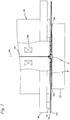
- FIG. 10 shows enlarged the lower end of barrel 34, metrology frame 40, an opening member 16A, and stage 22 that the exposure apparatus according to the second embodiment is equipped with.
- opening member 16A is provided instead of opening member 16 previously described and a laser interferometer system 128 is provided instead of encoder system 28, and by laser interferometer system 128, position information of stage 22 that holds wafer W is to be measured in the XY plane in directions of three degrees of freedom or six degrees of freedom.
- the structure of other parts is similar to electron beam exposure apparatus 100 according to the first embodiment previously described.
- Opening member 16A is structured basically similar to opening member 16 previously described, but the following point is different. That is, with opening member 16A, grating RG is not formed on the surface facing wafer W (lower surface, the surface on the -Z side) and a plurality of temperature sensors 70 consisting of, for example, infrared sensors, is arranged in an array in the XY two-dimensional direction. The plurality of temperature sensors is embedded in opening member 16A in a state where the lower surface of the sensors is at a position almost at the same surface as the lower surface of opening member 16A.
- controller 60 controls the irradiation position of electron beam EB with respect to wafer W, based on temperature information measured by the plurality of temperature sensors 70 during the exposure operation of wafer W.
- controller 60 can control the irradiation position of electron beam EB with respect to wafer W based on the temperature information of wafer W measured by the plurality of temperature sensors without the exposure operation being interrupted, which can make drawing errors of the pattern due to non-linear thermal expansion of the wafer smaller when non-linear thermal expansion of the wafer occurs by the irradiation of electron beam EB.
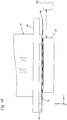
- FIG. 11 similar to FIG. 10 , shows enlarged the lower end of barrel 34, metrology frame 40, an opening member 16B, and stage 22 that the electron beam exposure apparatus according to the third embodiment is equipped with.
- opening member 16B is provided instead of opening member 16A previously described, and the apparatus is different from the electron beam exposure apparatus according to the second embodiment on the point that opening member 16B is supported by suspension from metrology frame 40 via a plurality of drivers 80 that can drive opening member 16B in a direction (the Z-axis direction) parallel to optical axis AX.
- the structure of other parts is similar to the electron beam exposure apparatus according to the second embodiment previously described.
- Opening member 16B is structured similar to opening member 16A, and other than having a plurality of temperature sensors 70 like opening member 16A, a structure is employed that makes it possible for opening member 16B to cool itself.
- a liquid flow path can be formed inside opening member 16B, and a structure can be employed in which opening member 16B cools itself by making a cooling liquid flow in the liquid flow path.
- a circulation system may be employed that makes the cooling liquid cooled in a cooler arranged external to the vacuum chamber flow into the liquid flow path via piping and returns the cooling liquid flowing in the liquid flow path to the cooler via piping.
- thermal conduction conduction, convection
- heat receiving amount by the radiation is inversely proportional to the square of the distance from the heat source.
- temperature rising rate of the wafer is inversely proportional to the square of the distance between opening member 16B and wafer W.
- controller 60 controls drivers 80 so that opening member 16B is moved close to wafer W to a desired distance based on detection results of temperature sensors 70, and cools wafer W to a predetermined temperature. Controller 60 can execute such cooling of wafer W when, for example, during the stepping operation (during deceleration and acceleration in the scanning direction) performed every predetermined times in the exposure operation of the wafer.
- processing for detection of the drift of electron beam EB should not to be performed at the time of stepping operation when cooling of wafer W is performed, and processing for detection of the drift of electron beam EB has to be performed at the time of stepping operation when cooling of wafer W is not performed, that is, at the time of stepping operation when the Z position of opening member 16B can be set to the position at the time of initial setting.
- the temperature sensors do not necessarily have to be provided.
- the temperature sensors provided may be one or several.
- opening member 16B instead of opening member 16B, opening member 16 previously described may be used, and instead of laser interferometer system 128, encoder system 28 may be employed.
- opening members 16A and 16B are used on which reflection surface 18a and calibration patterns CP are formed on the upper surface of the inner bottom wall of engraved recess section 16b
- the embodiments are not limited to this, and an opening member may be used that has only opening 16c formed without having one of, or both of the reflection surface and the calibration patterns on the upper surface of the inner bottom wall of engraved recess section 16b. That is, an opening member may be used that has opening 16c formed substantially on the optical axis of electron beam optical system 32 and has temperature sensor 70 at a surface facing wafer W.
- the center section including recess section 16a and the remaining section may be structured by separate members.
- the center section can be structured by a disc-shaped member having parts similar to recess section 16a previously described in the center of the upper surface, engraved recess section 16b that has at least one of reflection surface 18a and calibration patterns CP formed, and opening 16c.
- opening members 16, 16A, and 16B are used for calibration of the drift of electron beam EB, in other words, these opening members can also be referred to as calibration members. Also, since reflection surface 18a is formed on opening members 16, 16A, and 16B, in other words, these opening members can also be referred to as reflection members. Furthermore, since calibration patterns CP are formed on opening members 16, 16A, and 16B, in other words, these opening members can also be referred to as pattern members.
- the structure of detecting the drift of position and the like of electron beam EB is not limited to this structure.
- a charged particle detector that directly detects electron beam EB may be used instead of reflected electron detection device 38.
- the charged particle detector only has to be arranged at the position where calibration patterns CP are formed in opening member 16 previously described, instead of calibration patterns CP.
- a first charged particle detector for example, a first charged particle detector can be used that has a structure in which a plurality of sets of a scintillator section which converts electrons to light and a photoelectric conversion device which converts light generated by the scintillator section to electric signals are arranged.
- a light guide for guiding the light generated by the scintillator section may be provided in between the scintillator section and the photoelectric conversion device.
- the scintillator section is provided in the periphery of opening 16c of opening member 16 and is equipped with a plurality of scintillators arranged with the first direction or the second direction serving as the periodic direction, and each of the plurality of scintillators is connected to the photoelectric conversion device.
- the photoelectric conversion device for example a photodiode, a photomultiplier tube or the like may be used.
- a detector having a two-layer structure formed by layering a silicon (Si) thin film and a photodiode may be used as another detector (a second charged particle detector) to directly detect electron beam EB.
- the Si thin film has a plurality of slits formed with periodic directions in the first direction and the second direction, and facing each slit of the Si thin film, photodiodes are provided which allows detection of electron beam EB that passes through each of the slits.
- opening member 16 By irradiating a target such as wafer W with electron beam EB, there may be cases when electrical charge of opening member 16 occurs. That is, organic matter derived from the resist or the like is adhered to opening member 16, and the electrical charge is accumulated on the organic matter. When electrical charge is accumulated in opening member 16 in this manner, the position of electron beam EB irradiated on wafer W varies due to the influence of the accumulated electrical charge on the electric field. Therefore, to prevent the accumulation of electrical charge in opening member 16, a structure of applying a conductive coating on the surface of opening member 16, and connecting this coating to a ground wire may be employed.
- the conductive coating is applied to a surface (lower surface) facing wafer W of opening member 16, or to a surface (upper surface) facing electron beam optical system 32.
- the coating and ground wire are preferably connected at a place distanced from opening 16c to avoid the connection influencing electron beam EB.
- opening member 16 instead of providing the conductive coating on the surface of opening member 16, by structuring opening member 16 to be separable into a first part and a second part in a direction orthogonal to the optical axis of electron beam optical system 32, and connecting the first part and the second part in a state with a conductive material in between the first part and the second part, it becomes possible to incorporate a conductive material layer in opening member 16. And by connecting the conductive material layer to the ground wire, even if the organic matter adhered to the surface of opening member 16 is charged, the electrical charge flows to the ground wire through the conductive material layer, therefore, the electrical charge is not accumulated on opening member 16.
- a structure of cleaning the organic matter adhered to opening member 10 may be employed to prevent the electrical charge from accumulating on opening member 16.
- gas such as ozone on opening member 16 reacting with the organic matter adhered to opening member 16 and making a reaction
- opening member 16 can be cleaned.
- a cleaning device having a supply port that blows gas onto the surface of opening member 16 and a recovery port that recovers the gas that has been blown, only has to be arranged below opening member 16.
- opening member 16 it is preferable to employ a structure of opening member 16 to suppress influence of external magnetic field to suppress (prevent) the external magnetic field of electron beam optical system 32 from affecting electron beam EB via opening member 16.
- a structure may be employed in which the outer periphery of opening member 16 is surrounded by a high magnetic permeability material such as permalloy to make a magnetic shield.
- the material of the shield since the material of the shield has higher magnetic permeability than the material of opening member 16, almost all magnetism from the outside passes through the shield and bypasses opening member 16. Therefore, opening member 16 becomes shielded from the external magnetic field, and it becomes possible to prevent electron beam EB from being affected by the external magnetic field
- an electron beam irradiation device employing a method using a variable shaped beam (rectangular beam) can be used in which the electron beam shape is changed into a rectangular shape by making the electron beam pass through a rectangular shaped hole called a forming aperture in several steps.
- electron beam irradiation device 30 integral with metrology frame 40 are supported in a suspended state from a top plate (ceiling wall) of the vacuum chamber via the three suspension support mechanisms 50a, 50b, and 50c, the embodiments are not limited to this, and electron beam irradiation device may be supported by a floor type body. Also, a structure may be employed in which electron beam irradiation device 30 can move with respect to stage 22.
- each of the embodiments above may also be suitably applied when producing a mask by forming fine patterns on a glass substrate.
- the electron beam exposure apparatus using an electron beam as the charged particle beam is described, each of the embodiments above can also be applied to an exposure apparatus using an ion beam and the like as the charged particle beam for exposure.
- Electronic devices such as semiconductor devices (micro devices) are manufactured through steps such as; a step for performing function/performance design of a device, a step for making a wafer from a silicon material, a lithography step for performing exposure (pattern drawing according to a designed pattern data) with respect to a wafer by the electron beam exposure apparatus and the exposure method according to the embodiments or the modified examples previously described, a development step for developing the wafer which has been exposed, an etching step for removing by etching an exposed member of an area other than the area where the resist remains, a resist removing step for removing the resist that is no longer necessary since etching has been completed, a device assembly step (including a dicing process, a bonding process, and a package process), and an inspection step.
- the lithography step since the exposure method described so far is executed using the exposure apparatus of the embodiments above and the device pattern is formed on the wafer, micro devices with high integration can be produced with good productivity.
- the charged particle beam exposure apparatus is suitable for use in a lithography process when manufacturing electronic devices such as semiconductor devices.
- the device manufacturing method of the present invention is suitable for manufacturing micro devices.
Landscapes
- Physics & Mathematics (AREA)
- General Physics & Mathematics (AREA)
- Analytical Chemistry (AREA)
- Chemical & Material Sciences (AREA)
- Engineering & Computer Science (AREA)
- Health & Medical Sciences (AREA)
- Plasma & Fusion (AREA)
- Toxicology (AREA)
- Environmental & Geological Engineering (AREA)
- Epidemiology (AREA)
- Public Health (AREA)
- Exposure And Positioning Against Photoresist Photosensitive Materials (AREA)
- Electron Beam Exposure (AREA)
- Optics & Photonics (AREA)
Abstract
Description
- The present invention relates to a charged particle beam exposure apparatus and a device manufacturing method, and more particularly to a charged particle beam exposure apparatus that exposes a target with a charged particle beam, and a device manufacturing method that uses the charged particle beam exposure apparatus.
- In an exposure apparatus used in a lithography process to produce electronic devices (micro devices) such as a semiconductor device that uses ultraviolet light from far ultraviolet region to vacuum ultraviolet region as an exposure beam (hereinafter called an ultraviolet light exposure apparatus), in order to increase resolution, shortening exposure wavelength, optimizing illumination conditions, applying a liquid immersion method to further increase numerical aperture of a projection optical system and the like have been performed.
- In recent years, to form circuit patterns having a pitch finer than the resolution limit of the ultraviolet light exposure apparatus, an electron beam exposure apparatus has been proposed that forms spots smaller than the resolution limit of the ultraviolet light exposure apparatus with an electron beam and relatively scans this spot of the electron beam and a wafer (for example, refer to PTL 1).
- However, in the conventional electron beam exposure apparatus, irradiation of the electron beam causes a charge-up in targets such as a wafer, and by the influence of the electrical charge accumulated on the surface, the electron beam could be adversely affected.
- [PTL 1]
U.S. Patent No. 7,173,263 - According to a first aspect of the present invention, there is provided a charged particle beam exposure apparatus exposing a target with a charged particle beam, comprising: a stage holding the target that can be relatively moved with respect to the charged particle beam; a charged particle beam optical system irradiating the target with the charged particle beam; and a charged particle detection device arranged at an emitting side of the charged particle beam of the charged particle beam optical system and in the periphery of the charged particle beam, to detect the charged particle beam.
- According to a second aspect of the present invention, there is provided a charged particle beam exposure apparatus exposing a target with a charged particle beam, comprising: a stage, holding the target that can be relatively moved with respect to the charged particle beam; a charged particle beam optical system, irradiating the target with the charged particle beam; and an opening member arranged at an emitting side of the charged particle beam of the charged particle beam optical system, having an opening formed, through which the charged particle beam passes.
- According to a third aspect of the present invention, there is provided a device manufacturing method, including: exposing the substrate using the charged particle beam exposure apparatus according to one of the first and the second aspect, and developing the substrate that has been exposed.
-
-
FIG. 1 is a view schematically showing a structure of an electronbeam exposure apparatus 100 according to a first embodiment. -
FIG. 2 is an enlarged view of a lower end of a barrel, a metrology frame, and an opening member inFIG. 1 partly broken, along with a stage. -
FIG. 3A is a perspective view when viewing the opening member from above obliquely, andFIG. 3B is a planar view of the opening member. -
FIG. 4 is an enlarged view of the part circle A shown inFIG. 2 of the opening member. -
FIG. 5 is an enlarged view of the part circle B shown inFIG. 4 . -
FIG. 6 is a view showing an arrangement of a reflected electron detection device, along with a view showing a state of detection of reflected electrons from alignment marks. -
FIG. 7 is a block diagram showing an input-output relation of a controller that structures a control system of the electron beam exposure apparatus. -
FIG. 8 is a view showing a state where reflected electrons RE are detected using reflected electron detection device 38y1 when acquiring positions of calibration patterns on a reflection surface positioned at the +Y side of opening 16c. -
FIG. 9 is a view used to explain a modified example of the first embodiment. -
FIG. 10 is a view used to explain a structure of an electron beam exposure apparatus according to a second embodiment. -
FIG. 11 is a view used to explain a structure of an electron beam exposure apparatus according to a third embodiment. - Hereinafter, a first embodiment will be described, based on
FIGS. 1 to 8 .FIG. 1 schematically shows a structure of an electronbeam exposure apparatus 100 according to the first embodiment. Electronbeam exposure apparatus 100 is equipped with an electron beam optical system to be described later on; therefore, the description below will be made with a Z-axis being parallel to the optical axis of the electron beam optical system, and a Y-axis and an X-axis being orthogonal to each other in a plane perpendicular to the Z-axis. - In the embodiment, as an example of a charged particle beam, a structure using an electron beam will be described. The charged particle beam, however, is not limited to the electron beam, and may be a beam using a charged particle such as an ion beam.
- Electron
beam exposure apparatus 100 is equipped with avacuum chamber 10, and anexposure system 20 housed inside anexposure chamber 12 divided byvacuum chamber 10. -
Exposure system 20, as is shown inFIG. 1 , is equipped with astage 22 movable holding a wafer W, and an electronbeam irradiation device 30 that has an electron beamoptical system 32 which irradiates wafer W coated with a resist for electron beams (sensitive agent) with an electron beam. -
Stage 22 is moved with predetermined strokes in an X-axis direction and a Y-axis direction on a base member (not shown) by a stage drive system 24 (not shown inFIG. 1 , refer toFIG. 7 ) including a linear motor or the like, and is also finely moved in a Z-axis direction, a rotation direction around the X-axis (θx direction), a rotation direction around the Y-axis (θy direction), and a rotation direction around the Z-axis (θz direction). To suppress the irradiation position of the electron beam emitted from electronbeam irradiation device 30 on wafer W from moving (displacement) by variation of magnetic field caused by the linear motor or the like as much as possible, a magnetic shield is applied to the linear motor, and magnetic flux leakage from the linear motor to the wafer side is effectively suppressed or prevented. - Electron
beam irradiation device 30, as is shown inFIG. 1 , has abarrel 34. Thisbarrel 34 is formed in a cylindrical shape.Barrel 34 has an electronbeam emitting section 34a, amain section 34b that houses an electron gun section and an electromagnetic lens to be described later on, and a step section (flange section) arranged in between the electronbeam emitting section 34a andmain section 34b.Barrel 34 is supported from below by ametrology frame 40 consisting of an annular plate member. To be more specific, electronbeam emitting section 34a ofbarrel 34 is formed by a small diameter section whose diameter is smaller thanmain section 34b, and the small diameter section is inserted into a circular opening inmetrology frame 40 so thatbarrel 34 is supported from below bymetrology frame 40 in a state where the bottom surface of the step section is in contact with the upper surface ofmetrology frame 40. -
Metrology frame 40 has, to the outer periphery section, each of the lower end of threesuspension support mechanisms suspension support mechanism 50c inFIG. 1 is hidden in the depth of 50a) connected, arranged apart at a center angle of 120 degrees, and is supported in a suspended state from a top plate (ceiling wall) ofvacuum chamber 10 that dividesexposure chamber 12 viasuspension support mechanisms beam irradiation device 30 is supported by suspension at three points with respect tovacuum chamber 10. - The three
suspension support mechanisms suspension support mechanism 50a inFIG. 1 , each has a passivevibration isolation pad 52 provided at the upper end of each of the suspension support mechanisms, and awire 54 made of steel having one end connected to the lower end of vibration isolation pad (vibration isolation section) 52 and the other end connected tometrology frame 40.Vibration isolation pad 52 is fixed to the top plate ofvacuum chamber 10, and each includes an air damper or a coil spring. - In the embodiment, of vibration such as floor vibration transmitted from the outside to
vacuum chamber 10, since a large part of the vibration component in the Z-axis direction parallel to an optical axis AX of electron beamoptical system 32 is absorbed byvibration isolation pad 52, high vibration isolation performance can be obtained in the direction parallel to optical axis AX of electron beamoptical system 32. Also, natural frequency ofsuspension support mechanisms optical system 32. Since the threesuspension support mechanisms suspension support mechanisms vacuum chamber 10 from traveling to electron beam irradiation device 30) in the direction perpendicular to optical axis AX becomes sufficiently high. In this structure, while high vibration isolation performance can be obtained along with being able to largely reduce the weight of the mechanism section, relative position between electronbeam irradiation device 30 andvacuum chamber 10 may change at a comparatively low frequency. Therefore, in order to maintain the relative position between electronbeam irradiation device 30 andvacuum chamber 10 to a predetermined state, a positioning device 14 (not shown inFIG. 1 , refer toFIG. 7 ) of a non-contact method is provided in between electronbeam irradiation device 20 andvacuum chamber 10. Thispositioning device 14 can be structured including a six-axis acceleration sensor and a six-axis actuator, as is disclosed in, for example, International PublicationWO 2007/077920 , and the like.Positioning device 14 is controlled by a controller 60 (refer toFIG. 7 ). This allows the relative position of electronbeam irradiation device 30 in the X-axis direction, the Y-axis direction, the Z-axis direction and relative rotation angle around the X-axis, the Y-axis, and the Z-axis with respect tovacuum chamber 10 to be maintained at a constant state (a predetermined state). - Electron
beam irradiation device 30, as is shown inFIG. 1 , includes parts such as anelectron gun section 36 partly provided insidebarrel 34 that generates electrons and performs acceleration by an acceleration power supply (not shown) to form an electron beam EB (refer toFIG. 2 ), and an electron beamoptical system 32 arranged in a predetermined positional relation insidebarrel 34 that is structured of various electrodes and the like such as an electromagnetic lens and an aperture used to perform forming of spots of electron beam EB, adjustment of irradiation position of electron beam EB with respect to wafer W, adjustment of irradiation amount and the like. Electromagnetic lens includes an electromagnetic lens that has a focus coil (hereinafter referred to as a focus lens for convenience), an electromagnetic lens that has a deflection coil (hereinafter referred to as a deflection lens for convenience) and the like. -
FIG. 1 representatively shows afocus lens 32a anddeflection lens 32b that structure electron beamoptical system 32. As is shown inFIG. 7 ,focus lens 32a is controlled bycontroller 60 via afocus control section 64, anddeflection lens 32b is controlled bycontroller 60 via an electron beamdeflection control section 66. - In the embodiment, electron beam
optical system 32 consists of a multi-beam optical system that can be separately turned on/off and can irradiate n (n is, for example, 500) deflectable beams. As the multi-beam optical system, a system can be used that has a structure similar to the optical system disclosed in, for example, Japanese Unexamined Patent Application Publication No.2011-258842 WO 2007/017255 , and the like. As an example, when the 500 multi-beams arranged in a line in a lateral direction (X direction) are all in an on state (a state in which wafer W is irradiated with the electron beams), circular spots of the electron beams are formed simultaneously at 500 points set at an equal spacing within, for example, a 10 µm × 20 nm exposure area (a slit shaped area extending in the X direction). That is, one exposure area is formed with 500 electron beams. Note that the circular spot of the electron beam is formed having a diameter (e.g. a diameter of 20 nm) smaller than the resolution limit of the ultraviolet light exposure apparatus. - In the embodiment, by electron beam
optical system 32 forming spots of multiple (n=500) electron beams in a circular shape as is described above, arranging the circular spots in an exposure area, and also turning on/off the circular spots of the multiple electron beams while deflecting the circular spots, while movingstage 22 in a predetermined direction, e.g. Y-axis direction, in predetermined strokes at a constant speed so that wafer W is scanned with respect to the exposure area, apart of a shot area on the wafer, that is, a strip-shaped shot area having a width of 10 µm is exposed (scanning exposure). And, by repeatedly performing an alternate scanning operation in which the scanning exposure is performed alternately in the +Y direction and the -Y direction and a stepping operation in which wafer W (stage 22) is moved by a distance the same as the size of the exposure area in the X-axis direction to one side of the X-axis direction in deceleration and acceleration zones of wafer W (stage 22) in the Y-axis direction in order to change the scanning direction in the alternate scanning, the pattern is formed on the shot areas on the wafer. - Electron
beam irradiation device 30 is equipped with a reflected electron detection device to be described later on that detects reflected electrons. Electronbeam irradiation device 30 is controlled by controller60 (refer toFIG. 7 ). -
Controller 60 can deflect and scan electron beam EB by controllingdeflection lens 32b. Note that the range that electron beam EB can be scanned bydeflection lens 32b can be decided by the deflectability ofdeflection lens 32b. For example, the scanning range of electron beam EB can be set smaller than at least the radius ofbarrel 34. - In electron
beam exposure apparatus 100, on a -Z side of electron beam irradiation device 30 (electron beam optical system 32) and also on the +Z side of wafer W held bystage 22 in the Z-axis direction, that is, on the electron beam emitting side of electron beam irradiation device30, an openingmember 16 is arranged. Openingmember 16 is arranged, for example, parallel to an XY plane, which is a surface intersecting the optical axis of electron beamoptical system 32, and is supported in a suspended state frommetrology frame 40 via a plurality of (at least three)support members 42. Openingmember 16 has strength strong enough to maintain flatness in a state supported by the plurality ofsupport members 42. -
FIG. 2 shows an enlarged view of the lower end ofbarrel 34,metrology frame 40, and openingmember 16 inFIG. 1 in a state partly broken, along withstage 22. Also,FIGS. 3A and 3B show a perspective view of openingmember 16 when viewed from above obliquely and a planar view, respectively. Also,FIG. 4 shows the part of circle A inFIG. 2 of openingmember 16 enlarged, andFIG. 5 shows the part of circle B inFIG. 4 enlarged. - Opening
member 16, as is shown inFIGS. 3A and 3B , consists of a plate member having a shape almost a square, and aconical recess section 16a is formed in the center.Conical recess section 16a is formed so that the size of the opening gradually becomes smaller from the upper surface (electron beam optical system 32) side of openingmember 16 towards the lower surface (wafer W) side. As the material of openingmember 16, for example, a dielectric is used. Note that in the embodiment, as openingmember 16, a dielectric material also having a low thermal expansion coefficient such as, e.g. a zero expansion ceramic, is used. - In the center of recess section16a, as is shown in
FIG. 5 , anengraved recess section 16b of a circular cross section having, for example, a diameter D of about 100 µm to 200 µm is formed, and in the center of the bottom wall section of engravedrecess section 16b, a fine rectangular slit (or a circle) shapedopening 16c is formed.Opening 16c is slightly larger than an exposure field, having a size of about 30 µm. - On the upper surface of the bottom wall of engraved
recess section 16b, ametal reflection film 18 is provided, and on the upper surface ofreflection film 18, areflection surface 18a is formed. In other words,reflection surface 18a is provided aroundopening 16c. Also, the upper surface of the bottom wall is provided to face electron beamoptical system 32. Onreflection surface 18a at both sides of opening 16c in a first direction (the Y-axis direction inFIG. 5 ), a calibration pattern consisting of a line-and-space pattern whose periodic direction is in the first direction is formed, and onreflection surface 18a at both sides of opening 16c in a second direction (a direction orthogonal to the first direction, the X-axis direction inFIG. 5 ), a calibration pattern CP (inFIG. 5 and the like, only Y calibration pattern CP whose periodic direction is on the Y-axis direction is shown) consisting of a line-and-space pattern whose periodic direction is in the second direction is formed. Calibration pattern CP each has different reflectance in the line section and the space section. InFIG. 5 and the like, calibration pattern CP shown is made much thicker than the actual size of thickness for convenience of explanation. - Thickness t of the bottom wall (including the thickness of reflection film 18) of engraved
recess section 16b on whichreflection film 18 and calibration pattern CP are formed is desirably as thin as possible. In the embodiment, the thickness of the bottom wall of engravedrecess section 16 is set, as an example, to about 10 µm to 50 µm. - Note that in the embodiment, while
reflection surface 18a is a plane parallel to the XY plane, the embodiment is not limited to this, and may be a curved surface that has an arc shape in a side view whose center is on the optical axis of electron beamoptical system 32, or may be an inclined surface corresponding thereto. Also,reflection surface 18a may be formed separated in the first direction (Y-axis direction) and the second direction (X-axis direction). - Returning to the former subject of the description, inside
barrel 34, as is shown inFIG. 6 , a plurality of reflected electron detection devices 38 is provided near the lower end ofdeflection lens 32b of electron beamoptical system 32. In other words, the plurality of reflected electron detection devices 38 is arranged on the emitting side ofdeflection lens 32b and also at the periphery of charged particle beams. Note that the periphery of charged particle beams refers to the range in which electron beams EB can be scanned bydeflection lens 32b as is previously described. - Each of the plurality of reflected electron detection devices 38 is structured, for example, by a semiconductor detector, and sends detection signals corresponding to reflected electrons which are detected to a signal processor 62 (refer to
FIG. 7 ).Signal processor 62, after amplifying the detection signals of the plurality of reflected electron detection devices 38 with an amplifier (not shown), performs signal processing and sends the processing results to controller 60 (refer toFIG. 7 ). - Each of the plurality of reflected electron detection devices 38, as is shown in
FIG. 6 , is provided at a position where reflected electrons generated at an alignment mark AM that entersbarrel 34 viaopening 16c and the inner space of engravedrecess section 16b can be detected when alignment mark AM on wafer W is irradiated with electron beam EB via the inner space of engravedrecess section 16b andopening 16c of openingmember 16. Alignment mark AM formed on wafer W is formed by a two-dimensional mark including a line-and-space pattern whose periodic direction is in the Y-axis direction (the first direction) and a line-and-space pattern whose periodic direction is in the X-axis direction (the second direction). AlthoughFIG. 6 only shows a pair of reflected electron detection devices 38y1 and 38y2 that detects reflected electrons generated in a direction tilted with respect to the optical axis within a YZ plane from alignment mark AM on wafer W, a pair of reflected electron detection devices 38x1 and 38x2 that detects reflected electrons generated in a direction tilted with respect to the optical axis within an XZ plane from alignment mark AM is also actually provided (refer toFIG. 7 ). In the embodiment, reflected electron detection devices 38x1, 38x2, 38y1, and 38y2 are also used when performing calibration of beam position to be described later on. - Position information of
stage 22 is measured by an encoder system 28 (refer toFIG. 7 ).Encoder system 28, as is shown inFIG. 2 , is formed in an area excluding a section at the rear surface side of recess section16a at the lower surface (surface on the -Z side) of openingmember 16, and consists of a grating RG consisting of a reflection type two-dimensional grating whose periodic directions are in the X-axis direction and the Y-axis direction and four heads 26 (hereinafter described asheads 261 to 264 for convenience) with one head arranged at one corner of the four corners ofstage 22 facing grating RG. - As the reflection type two-dimensional grating, a reflective diffraction grating having a pitch of, e.g. 1 µm, for each of the periodic directions is used. Note that as grating RG, a grating structured of four sections that can individually face the four
heads 26 may be used, as is disclosed in, for example,U.S. Patent Application Publication No. 2011/0053061 . - Of the two diagonal lines of
stage 22, near the two corners located on one of the diagonal lines, heads 261 and 263 are provided whose measurement directions are in the X-axis direction and the Z-axis direction, and near the two corners located on the other diagonal line, heads 262 and 264 are provided whose measurement directions are in the Y-axis direction and the Z-axis direction. The four heads 261 to 264 are arranged at each of the vertex positions of the same square or rectangle in a planar view.FIG. 2 shows only twoheads -
Heads linear encoders stage 22 in the X-axis direction and the Z-axis direction. Also, heads 262 and 264 make up two-axislinear encoders stage 22 in the Y-axis direction and the Z-axis direction. - As each of the
heads 261 to 264, an encoder head having a structure similar to a displacement measurement sensor head disclosed in, for example,U.S. Patent No. 7,561,280 can be used. - The four two-axis
linear encoders 281 to 284 described above, that is, the fourheads 261 to 264 which measure position information ofstage 22 using each grating RGstructure encoder system 28. Position information measured byencoder system 28 is supplied to controller 60 (refer toFIG. 7 ). - In
encoder system 28, at least three of the fourheads 261 to 264 faces grating RG at all times whenstage 22 is in an area where exposure and alignment to wafer W is performed, therefore,controller 60 can measure the position of stage 22 (wafer W) in directions of six degrees of freedom (in each of the X-axis, the Y-axis, the Z-axis, the θx, the θy, and the θz directions), based on the information measured byencoder system 28. -
FIG. 7 is a block diagram showing an input-output relation ofcontroller 60 which structures a control system of electronbeam exposure apparatus 100.Controller 60 includes a microcomputer and the like, and has overall control over each section of electronbeam exposure apparatus 100 including the sections shown inFIG. 7 . - In electron
beam exposure apparatus 100 structured in the manner described above,controller 60 controls electron beam EB emitted from electron beamoptical system 32 andstage 22 according to a predetermined pattern data and each drawing parameter decided in advance, and performs exposure (pattern drawing) with respect to wafer W. - Now, in order to complete a micro device such as a semiconductor device, a plurality of layers of patterns has to be overlaid and formed on a wafer, which makes overlay between an underlayer pattern and a pattern to be drawn important.
- Therefore, in the embodiment, prior to pattern drawing (exposure of the wafer) with respect to the wafer, by
controller 60controlling deflection lens 32b via electron beamdeflection control section 66, electron beam EB is sequentially scanned with respect to two or more alignment marks AM (refer toFIG. 6 ) formed in advance on the wafer, and on this scanning, reflected electrons generated from alignment marks AM are detected by reflected electron detection device 38. At the time of scanning with respect to alignment marks AM, accelerating voltage of electron beam EB is set to the same accelerating voltage as the time of exposure (the time of pattern drawing). -
FIG. 6 , as an example, shows reflected electrons RE of electron beam EB irradiated on alignment marks AM along an optical path (an optical path indicated by a solid line in the drawing) parallel to the optical axis, moving toward reflected electron detection devices 38y1 and 38y2 from alignment marks AM.Controller 60 specifies the position of alignment marks AM based on deflection information (information including deflection angle, deflection direction and the like) of the electron beam obtained from electron beamdeflection control section 66 and processing results of detection signals of the marks obtained fromsignal processor 62, and based on the position and stage coordinate information obtained fromencoder system 28 at the time of detection, acquires the position of alignment marks AM on a stage coordinate system. Based on the position on the stage coordinate system of the two or more alignment marks acquired in this manner, target position information for positioning the shot areas on the wafer to an exposure position (irradiation position in a reference state of the electron beam, that is, irradiation position of electron beam EB on wafer W when electron beam EB is irradiated along the optical path indicated by the solid line inFIG. 6 on optical axis AX) can be acquired. Then, based on the target position information that has been obtained,controller 60 draws the pattern while moving the wafer (stage 22) at the time of exposure of the wafer (at the time of pattern drawing with respect to the wafer). By using alignment marks AM as a reference as is described, the pattern can be drawn at a desired position at all times, and a new pattern to be drawn can be overlaid favorably on the pattern which has already been formed on wafer W. - However, while using electron
beam exposure apparatus 100, when the position of electron beam EB drifts from the reference state, for example, drifts from a state where the optical path of electron beam EB coincides with optical axis AX of electron beamoptical system 32 due to, for example, thermal expansion and the like ofbarrel 34 housing electron beamoptical system 32, even if exposure (pattern drawing) with respect to the wafer by electron beam EB is performed with alignment marks AM serving as a reference as is described above, the pattern cannot be drawn at a desired position due to the drift. Also, drift of focus of electron beam EB also becomes a cause of defective exposure. - Therefore, in the embodiment,
controller 60 performs initial setting for calibration of drift (position and focus) of electron beam EB at the time of alignment measurement before starting exposure, prior to measuring mark position information of alignment marks AM. -
Controller 60 sets the position of wafer W in the Z-axis direction to the same position as the time of exposure and scans alignment marks AM while changing focal position by changing current of a focus coil that focuslens 32a described earlier has viafocus control section 64, and from a change in detection signals of reflected electron detection device 38 (a predetermined one among 38x1, 38x2, 38y1, and 38y2) that has detected reflected electron RE, the position where the change is sharpest is acquired as the optimum focal position, and the current corresponding to the optimum focal position is to be supplied thereafter to the focus coil. - Next,
controller 60 deflects and scans electron beam EB with respect to the four calibration patterns CP onreflection surface 18a and detects reflected electrons from each of the calibration patterns CP using reflected electron detection devices 38x1, 38x2, 38y1, and 38y2, and based on deflection information of electron beam EB obtained from electron beamdeflection control section 66 and information on processing results of detection signals of calibration patterns CP obtained fromsignal processor 62, position (hereinafter referred to as position information of calibration patterns CP) of calibration patterns CP with the position of electron beam EB in the reference state serving as a reference, that is, information on the amount of angle that electron beam EB should be deflected in each of the X direction and the Y direction from the reference state or on the direction of deflection so that the center position of each of the calibration patterns CP is made to be irradiated with electron beam EB is to be acquired.FIG. 8 , as an example, shows a state where reflected electrons RE are detected using reflected electron detection device 38y1 when acquiring position information of calibration pattern CP on the reflection surface positioned at the +Y side ofopening 16c. Here, as is obvious from the position information of calibration pattern CP defined above, in the case the position information of the calibration pattern has changed later on from the position information at the time of the initial setting, this means that the position of the electron beam has drifted according to the amount of change. Drift includes deviation of deflection angle, shift of deflection direction, and shift with respect to optical axis AX. Also,controller 60 functions as a detection device that detects the drift. - On this operation,
controller 60 stores the state of change of detection signals of a predetermined one reflected electron detector that has detected reflected electrons from calibration patterns CP, such as, for example, reflected electron detection device 38y1, in an internal memory. This is becausecontroller 60 detects the drift of focus of electron beam EB later on, using the state of change of detection signals as a reference. Note that all reflected electron detection devices may have the state of change of detection signals stored in the internal memory. - This completes the initial setting for calibration of drift (position and focus) of electron beam EB.
- After this, measurement (alignment measurement) of mark position information of alignment marks AM described earlier is performed.
- Then,
controller 60 acquires the target position information to position the shot areas on the wafer at the exposure position as is previously described based on results of the alignment measurement, and at the time of exposure on the wafer (at the time of pattern drawing with respect to the wafer), draws the pattern while moving the wafer (stage 22) based on the acquired target position information. This wafer exposure (pattern drawing), as is described earlier, is performed, by repeating the alternate scanning operation in which scanning exposure of the wafer is performed alternately in the +Y direction and the -Y direction and the operation (stepping operation) of moving the wafer by a distance the same as the width of the exposure area in the X-axis direction to one side of the X-axis direction during deceleration and acceleration of the wafer in the Y-axis direction between scanning in the +Y direction (plus scan) and scanning in the -Y direction (minus scan). - However, since the size of the exposure area in a non-scanning direction (the X-axis direction) of electron
beam exposure apparatus 100 is about, e.g. 50 µm,, the alternate scanning operation has to be repeated many times in order to expose one wafer or one exposure area, the exposure operation takes much more time than the ultraviolet light exposure apparatus and the like. Therefore, the calibration of drift (position and focus) of electron beam EB has to be performed even while exposing one wafer. - Therefore, in electron
beam exposure apparatus 100, each time the stepping operation described earlier is performed, during the stepping operation,controller 60 deflects and scans electron beam EB with respect to the four calibration patterns CP onreflection surface 18a and detects reflected electrons RE generated from each of the calibration patterns CP using reflected electron detection devices 38x1, 38x2, 38y1, and 38y2, similar to the time of initial setting for calibration previously described. Then,controller 60 acquires position information of calibration patterns CP based on deflection information of the electron beam obtained from electron beamdeflection control section 66 and information on processing results of detection signals of calibration patterns CP obtained from the signal processor, and stores the information in memory. - Then,
controller 60 calculates the position of calibration patterns CP according to a procedure decided in advance, based on position information of calibration pattern CP obtained N times (N is a natural number, e.g. 10 times). For example, an average of the remaining position information which is information excluding from the 10 times the position that has changed maximum and minimum from the time of initial setting, position information that has changed maximum from the time of initial setting, or an average of the 10 times is acquired as the position of calibration patterns CP. Then, by comparing the calculated position and the position information of calibration patterns CP at the time of initial setting described above, the controller acquires the drift amount of the position of electron beam EB. Note that instead of the average of 10 times,controller 60 may acquire the average less than 10 times of moving. - Then,
controller 60 calibrates the drift each time the drift amount of the position of electron beam EB is acquired, or calibrates the drift only when the drift amount exceeds a threshold value. - Also,
controller 60 acquires the state of change of detection signals of reflected electrons RE from a predetermined calibration pattern CP once in every N times, compares the acquired state of change to the corresponding state of change of the detection signals stored at the time of initial setting, and detects the drift amount of the focus of the electron beam. Then,controller 60 calibrates the drift each time the drift amount of the focus of electron beam EB is acquired by adjusting the current supplied to the focus coil, or calibrates the drift only when the drift amount exceeds a threshold value. - As is described so far, with electron
beam exposure apparatus 100 according to the embodiment, since the exposure apparatus is equipped with the plate shaped openingmember 16 arranged facing wafer W via a predetermined gap on the wafer W side in the optical axis AX direction (the Z-axis direction) of electron beamoptical system 32, withopening 16c formed through which electron beam EB from electron beamoptical system 32 passes, this can suppress an adverse effect that the electrical charge accumulated on wafer W by irradiation of electron beam EB has on the irradiation position of electron beam EB when compared to the case when the exposure apparatus is not equipped with openingmember 16. Also, in the embodiment, especially since openingmember 16 is made of a dielectric (zero expansion ceramic), the adverse effect that the electrical charge accumulated on wafer W by irradiation of electron beam EB has on the irradiation position of electron beam EB can be suppressed more effectively. - Also, as is obvious from
FIG. 6 , since only reflected electrons RE having a high extraction angle that can pass through opening 16c of openingmember 16 are detected and reflected electrons of low energy or reflected electrons that are scattered nearstage 22 withinexposure chamber 12 are no longer detected when detecting the reflected electrons from alignment marks AM on wafer W with reflected electron detection device 38, as a consequence, S/N ratio when detecting the reflected electrons can be improved. - Also, with electron
beam exposure apparatus 100 according to the embodiment, electron beam EB is deflected and scanned with respect to calibration patterns CP onreflection surface 18a formed on the inner bottom surface of the engraved recess section of openingmember 16, and by detecting reflected electrons RE generated at calibration patterns CP with reflected electron detection device 38, the drift of position of electron beam EB is detected. Therefore, the drift of position of electron beam EB can be detected, without using the alignment marks on the wafer. Also, with electronbeam exposure apparatus 100,controller 60 detects the drift of position of electron beam EB during the stepping operation (during the deceleration and acceleration period in the scanning direction) in between the plus scan and the minus scan in the exposure operation of the wafer. Therefore, it becomes possible to detect the drift of position of electron beam EB and perform calibration of the drift, without decreasing the throughput. - Also, with electron beam exposure apparatus100, along with detecting the drift of position of electron beam EB, it is possible to detect the drift amount of focus of the electron beam, based on change of detection signals of the reflected electrons from the calibration pattern acquired for detecting the drift of position of electron beam EB, and to perform calibration of the drift of focus of electron beam EB when necessary.
- Note that in the embodiment, while the case has been described where the alignment marks formed on wafer W are scanned with the electron beam on the initial setting for calibration of the drift (position and focus) of electron beam EB, the embodiment is not limited to this, and the reference marks provided on
stage 22 may be scanned with the electron beam. In such a case, the scan becomes free of the risk of being affected by the electron beam resist coated on wafer W, being affected by defective shapes of alignment marks, and the like. In this case, a measurement device for measuring the positional relation between the alignment marks and the reference marks, such as for example, a microscope or the like will be necessary. - Next, a modified example of the electron beam exposure apparatus according to the first embodiment will be described. While the electron beam exposure apparatus according to the modified example, as is shown in
FIG. 9 , differs from the first embodiment previously described on the point that the calibration pattern is not formed onreflection surface 18a of openingmember 16, the structure of other parts are similar to the first embodiment previously described. - With the electron beam exposure apparatus according to the modified example, as is shown in
FIG. 9 ,controller 60 scans electron beam EB via electron beamdeflection control section 66 with respect toreflection surface 18a in a range including a border section with the opening (edge ofreflection surface 18a). This allowscontroller 60 to detect reflected electrons fromreflection surface 18a using reflected electron detection devices 38x1, 38x2, 38y1, and 38y2 and to detect position of the edge ofreflection surface 18a with the position of electron beam EB serving as a reference, based on deflection information of electron beam EB obtained from electron beamdeflection control section 66 and information on processing results of detection signals ofreflection surface 18a obtained fromsignal processor 62, similar to the detection of position information of calibration pattern CP previously described. - Accordingly, in the modified example, by handling the position of the edge of
reflection surface 18a in a manner similar to the position of calibration patterns CP in the embodiment described above, it becomes possible to perform detection of the drift of position of electron beam EB and calibration of the drift in the same way as the embodiment described above. In the modified example, in both initial setting and during stepping operation, as is shown inFIG. 9 ,controller 60 scans electron beam EB via electron beamdeflection control section 66 with respect to reflection surface18a in a range including the edge ofreflection surface 18a. - Also, since detection signals of reflected electrons from
reflection surface 18a including the edge are obtained by scanning electron beam EB with respect toreflection surface 18a, it becomes possible to detect drift amount of the focus of the electron beam based on change of the detection signals, and to perform calibration of the drift of the focus of electron beam EB when necessary. - Note that in the first embodiment and the modified example described above, while
reflection surface 18a is formed on the upper surface of the bottom wall of engravedrecess section 16b of openingmember 16, a reflection pattern having a reflectance to electron beam EB different from that of the upper surface may be formed on the upper surface of the bottom wall ofrecess section 16b, without the reflection surface being formed. In this case, by handling the reflection pattern in a manner similar to the calibration pattern in the embodiment described above, the same working effect can be produced as the embodiment described above. - Note that in the embodiment above, while opening
member 16 is supported bymetrology frame 40 which supports barrel 34 (electron beam irradiation device 30) having electron beamoptical system 32 inside, positional relation between openingmember 16 and metrology frame 4 0 may change by the influence of heat or influence of other factors. Therefore, for example, as is shown inFIG. 7 in a dotted (broken line) block, ameasurement device 90 that measures the relative position betweenmetrology frame 40 and openingmember 16 may be further provided, andcontroller 60 may correct the position of electron beam EB based on measurement information of the measurement device. - Note that in the embodiment above, while the case has been described in which opening
member 16 is supported bymetrology frame 40 supporting barrel 34 (electron beam irradiation device 30) that has electron beamoptical system 32 inside, the embodiment is not limited to this, and the positional relation of openingmember 16 with electron beam optical system 32 (barrel 34) may be constantly maintained. In this case,measurement device 90 described above may be provided, and bycontroller 60 or another controller controlling an actuator (not shown), openingmember 16 may be driven with respect tometrology frame 40 so that a constant positional relation is maintained between electron beam optical system 32 (barrel 34) supported bymetrology frame 40 and openingmember 16. - Also, in the embodiment above, while an example was given where position information of
stage 22 is measured byencoder system 28 that has grating RG formed on the lower surface (surface on the -Z side) of openingmember 16 and fourheads 26 provided on the upper surface ofstage 22 at the four corners facing the grating, the embodiment is not limited to this, and the position information ofstage 22 may be measured by an encoder system in which the grating section (grating) is provided atstage 22 and the heads are provided external to stage 22 in a manner that can face the grating section. - Also, the position measurement device that measures position information of
stage 22 is not limited to the encoder system, and a laser interferometer system may also be used. - Next, a second embodiment will be described, based on
FIG. 10 . Here, the same reference codes will be used for component parts identical or similar to electronbeam exposure apparatus 100 according to the first embodiment previously described, and the description thereabout will be brief or omitted. -
FIG. 10 shows enlarged the lower end ofbarrel 34,metrology frame 40, an openingmember 16A, andstage 22 that the exposure apparatus according to the second embodiment is equipped with. With the electron beam exposure apparatus according to the second embodiment, openingmember 16A is provided instead of openingmember 16 previously described and alaser interferometer system 128 is provided instead ofencoder system 28, and bylaser interferometer system 128, position information ofstage 22 that holds wafer W is to be measured in the XY plane in directions of three degrees of freedom or six degrees of freedom. The structure of other parts is similar to electronbeam exposure apparatus 100 according to the first embodiment previously described. - Opening
member 16A is structured basically similar to openingmember 16 previously described, but the following point is different. That is, with openingmember 16A, grating RG is not formed on the surface facing wafer W (lower surface, the surface on the -Z side) and a plurality oftemperature sensors 70 consisting of, for example, infrared sensors, is arranged in an array in the XY two-dimensional direction. The plurality of temperature sensors is embedded in openingmember 16A in a state where the lower surface of the sensors is at a position almost at the same surface as the lower surface of openingmember 16A. - Then,
controller 60 controls the irradiation position of electron beam EB with respect to wafer W, based on temperature information measured by the plurality oftemperature sensors 70 during the exposure operation of wafer W. - With the electron beam exposure apparatus according to the second embodiment, other than being able to obtain the same effect as the first embodiment previously described,
controller 60 can control the irradiation position of electron beam EB with respect to wafer W based on the temperature information of wafer W measured by the plurality of temperature sensors without the exposure operation being interrupted, which can make drawing errors of the pattern due to non-linear thermal expansion of the wafer smaller when non-linear thermal expansion of the wafer occurs by the irradiation of electron beam EB. - Next, a third embodiment will be described, based on
FIG. 11 . Here, the same reference codes will be used for component parts identical or similar to the electron beam exposure apparatus according to the first and second embodiments previously described, and the description thereabout will be brief or omitted. -
FIG. 11 , similar toFIG. 10 , shows enlarged the lower end ofbarrel 34,metrology frame 40, an openingmember 16B, andstage 22 that the electron beam exposure apparatus according to the third embodiment is equipped with. With the electron beam exposure apparatus according to the third embodiment, openingmember 16B is provided instead of openingmember 16A previously described, and the apparatus is different from the electron beam exposure apparatus according to the second embodiment on the point that openingmember 16B is supported by suspension frommetrology frame 40 via a plurality ofdrivers 80 that can drive openingmember 16B in a direction (the Z-axis direction) parallel to optical axis AX. The structure of other parts is similar to the electron beam exposure apparatus according to the second embodiment previously described. - Opening
member 16B is structured similar to openingmember 16A, and other than having a plurality oftemperature sensors 70 like openingmember 16A, a structure is employed that makes it possible for openingmember 16B to cool itself. For example, a liquid flow path can be formed inside openingmember 16B, and a structure can be employed in which openingmember 16B cools itself by making a cooling liquid flow in the liquid flow path. For example, a circulation system may be employed that makes the cooling liquid cooled in a cooler arranged external to the vacuum chamber flow into the liquid flow path via piping and returns the cooling liquid flowing in the liquid flow path to the cooler via piping. - While thermal conduction (conduction, convection) through air does not occur inside the vacuum chamber since there is no air, it is possible to cool wafer W facing opening
member 16B by radiation (emission) with openingmember 16B. Also, heat receiving amount by the radiation is inversely proportional to the square of the distance from the heat source. In the case of the third embodiment, temperature rising rate of the wafer is inversely proportional to the square of the distance between openingmember 16B and wafer W. - Therefore, in the third embodiment, according to the thermal conduction property by the radiation described above,
controller 60controls drivers 80 so that openingmember 16B is moved close to wafer W to a desired distance based on detection results oftemperature sensors 70, and cools wafer W to a predetermined temperature.Controller 60 can execute such cooling of wafer W when, for example, during the stepping operation (during deceleration and acceleration in the scanning direction) performed every predetermined times in the exposure operation of the wafer. However, in this case, when detection and calibration of the drift of electron beam EB similar to electronbeam exposure apparatus 100 according to the first embodiment previously described is to be performed, because Z position of openingmember 16B changes from the time of initial setting at the time of stepping operation when cooling of wafer W is performed, even if detection of reflected electrons from calibration patterns CP previously described is performed, detection results of the reflected electrons cannot be used for detecting the drift of electron beam EB. Accordingly, processing for detection of the drift of electron beam EB should not to be performed at the time of stepping operation when cooling of wafer W is performed, and processing for detection of the drift of electron beam EB has to be performed at the time of stepping operation when cooling of wafer W is not performed, that is, at the time of stepping operation when the Z position of openingmember 16B can be set to the position at the time of initial setting. - Note that in the third embodiment described above, since the temperature rise of wafer W due to irradiation of electron beam EB can be acquired in advance by simulation or the like, it is also possible to control
driver 80 during the stepping operation previously described to cool wafer W, based on the simulation results. In such a case, the temperature sensors do not necessarily have to be provided. As is obvious from the description here, in the third embodiment, the temperature sensors provided may be one or several. - Also, when no temperature sensors are provided in the third embodiment, instead of opening
member 16B, openingmember 16 previously described may be used, and instead oflaser interferometer system 128,encoder system 28 may be employed. - Note that in the second and third embodiments described above, while opening
members reflection surface 18a and calibration patterns CP are formed on the upper surface of the inner bottom wall of engravedrecess section 16b, the embodiments are not limited to this, and an opening member may be used that has only opening 16c formed without having one of, or both of the reflection surface and the calibration patterns on the upper surface of the inner bottom wall of engravedrecess section 16b. That is, an opening member may be used that hasopening 16c formed substantially on the optical axis of electron beamoptical system 32 and hastemperature sensor 70 at a surface facing wafer W. - Note that in each of the embodiments above, instead of opening
members recess section 16a and the remaining section may be structured by separate members. In this case, for example, the center section can be structured by a disc-shaped member having parts similar torecess section 16a previously described in the center of the upper surface, engravedrecess section 16b that has at least one ofreflection surface 18a and calibration patterns CP formed, andopening 16c. - Also, in each of the embodiments above, since opening
members reflection surface 18a is formed on openingmembers members - Note that in each of the embodiments above, while the case has been described where the drift of position and the like of electron beam EB is detected by deflecting and scanning electron beam EB with respect to calibration patterns CP on formed on opening
member 16, and by detecting reflected electrons RE generated at calibration patterns CP with reflected electron detection device 38, the structure of detecting the drift of position and the like of electron beam EB is not limited to this structure. For example, instead of reflected electron detection device 38, a charged particle detector that directly detects electron beam EB may be used. In this case, the charged particle detector only has to be arranged at the position where calibration patterns CP are formed in openingmember 16 previously described, instead of calibration patterns CP. - Here, as the charged particle detector, for example, a first charged particle detector can be used that has a structure in which a plurality of sets of a scintillator section which converts electrons to light and a photoelectric conversion device which converts light generated by the scintillator section to electric signals are arranged. Note that a light guide for guiding the light generated by the scintillator section may be provided in between the scintillator section and the photoelectric conversion device.
- In the first charged particle detector, the scintillator section is provided in the periphery of opening 16c of opening
member 16 and is equipped with a plurality of scintillators arranged with the first direction or the second direction serving as the periodic direction, and each of the plurality of scintillators is connected to the photoelectric conversion device. As the photoelectric conversion device, for example a photodiode, a photomultiplier tube or the like may be used. - Furthermore, as another detector (a second charged particle detector) to directly detect electron beam EB, a detector having a two-layer structure formed by layering a silicon (Si) thin film and a photodiode may be used. The Si thin film has a plurality of slits formed with periodic directions in the first direction and the second direction, and facing each slit of the Si thin film, photodiodes are provided which allows detection of electron beam EB that passes through each of the slits.
- Also by irradiating a target such as wafer W with electron beam EB, there may be cases when electrical charge of opening
member 16 occurs. That is, organic matter derived from the resist or the like is adhered to openingmember 16, and the electrical charge is accumulated on the organic matter. When electrical charge is accumulated in openingmember 16 in this manner, the position of electron beam EB irradiated on wafer W varies due to the influence of the accumulated electrical charge on the electric field. Therefore, to prevent the accumulation of electrical charge in openingmember 16, a structure of applying a conductive coating on the surface of openingmember 16, and connecting this coating to a ground wire may be employed. The conductive coating is applied to a surface (lower surface) facing wafer W of openingmember 16, or to a surface (upper surface) facing electron beamoptical system 32. The coating and ground wire are preferably connected at a place distanced from opening 16c to avoid the connection influencing electron beam EB. With this structure, even if the organic matter is adhered to openingmember 16, the electrical charge is not accumulated on the organic matter and is carried through the coating to the ground wire, which can reduce the influence on electron beam EB. - Note that instead of providing the conductive coating on the surface of opening
member 16, by structuring openingmember 16 to be separable into a first part and a second part in a direction orthogonal to the optical axis of electron beamoptical system 32, and connecting the first part and the second part in a state with a conductive material in between the first part and the second part, it becomes possible to incorporate a conductive material layer in openingmember 16. And by connecting the conductive material layer to the ground wire, even if the organic matter adhered to the surface of openingmember 16 is charged, the electrical charge flows to the ground wire through the conductive material layer, therefore, the electrical charge is not accumulated on openingmember 16. - A structure of cleaning the organic matter adhered to opening
member 10 may be employed to prevent the electrical charge from accumulating on openingmember 16. By blowing gas such as ozone on openingmember 16 reacting with the organic matter adhered to openingmember 16 and making a reaction, openingmember 16 can be cleaned. For example, after moving (withdrawing)stage 22 from below openingmember 16, a cleaning device, having a supply port that blows gas onto the surface of openingmember 16 and a recovery port that recovers the gas that has been blown, only has to be arranged below openingmember 16. - Note that it is preferable to employ a structure of opening
member 16 to suppress influence of external magnetic field to suppress (prevent) the external magnetic field of electron beamoptical system 32 from affecting electron beam EB via openingmember 16. For example, a structure may be employed in which the outer periphery of openingmember 16 is surrounded by a high magnetic permeability material such as permalloy to make a magnetic shield. In this structure, since the material of the shield has higher magnetic permeability than the material of openingmember 16, almost all magnetism from the outside passes through the shield andbypasses opening member 16. Therefore, openingmember 16 becomes shielded from the external magnetic field, and it becomes possible to prevent electron beam EB from being affected by the external magnetic field - Note that in each of the embodiments above, while examples were given in the case of using a single-column type electron beam
optical system 32, the embodiments are not limited to this, and a multi-column type electron beam optical system that has a plurality of optical system columns consisting of multi-beam optical systems previously described may also be used. Also,recess section 16a, engravedrecess section 16b, andopening 16c previously described only have to be formed in an arrangement corresponding to the plurality of optical system columns on the upper surface of each of the openingmembers - Note that in each of the embodiments above, while the case has been described where the
entire exposure system 20 is housed insidevacuum chamber 10, the embodiments are not limited to this, and ofexposure system 20, the part excluding the lower end ofbarrel 34 of electronbeam irradiation device 30 may be exposed outside ofvacuum chamber 10. - Note that in each of the embodiments above, while electron
beam irradiation device 30 integral withmetrology frame 40 are supported in a suspended state from a top plate (ceiling wall) of the vacuum chamber via the threesuspension support mechanisms beam irradiation device 30 can move with respect to stage 22. - Note that in each of the embodiments above, while the case has been described where the target is a wafer for manufacturing semiconductor devices, the exposure apparatus according to each of the embodiments may also be suitably applied when producing a mask by forming fine patterns on a glass substrate. Also, in each of the embodiments above, while the electron beam exposure apparatus using an electron beam as the charged particle beam is described, each of the embodiments above can also be applied to an exposure apparatus using an ion beam and the like as the charged particle beam for exposure.
- Electronic devices such as semiconductor devices (micro devices) are manufactured through steps such as; a step for performing function/performance design of a device, a step for making a wafer from a silicon material, a lithography step for performing exposure (pattern drawing according to a designed pattern data) with respect to a wafer by the electron beam exposure apparatus and the exposure method according to the embodiments or the modified examples previously described, a development step for developing the wafer which has been exposed, an etching step for removing by etching an exposed member of an area other than the area where the resist remains, a resist removing step for removing the resist that is no longer necessary since etching has been completed, a device assembly step (including a dicing process, a bonding process, and a package process), and an inspection step. In this case, in the lithography step, since the exposure method described so far is executed using the exposure apparatus of the embodiments above and the device pattern is formed on the wafer, micro devices with high integration can be produced with good productivity.
- Note that the disclosures of all publications, international publications, U.S. Patent Application Publications, and U.S. Patents related to the exposure apparatus and the like quoted in each of the embodiments above, in their entirety, are incorporated herein by reference as a part of the present specification.
- As is described so far, the charged particle beam exposure apparatus according to the present invention is suitable for use in a lithography process when manufacturing electronic devices such as semiconductor devices. Also, the device manufacturing method of the present invention is suitable for manufacturing micro devices.
-
- 16...opening member,
- 16c...opening,
- 18a...reflection surface,
- 22...stage,
- 2 6...head,
- 32...electron beam optical system,
- 38...reflected electron detection device,
- 40...metrology frame,
- 60...controller,
- 70...temperature sensor,
- 80...driver,
- 90...measurement device,
- 100...electron beam exposure apparatus,
- AX...optical axis,
- EB...electron beam,
- CP...calibration pattern,
- RG...grating,
- W...wafer.
Claims (40)
- A charged particle beam exposure apparatus exposing a target with a charged particle beam, comprising:a stage, holding the target that can be relatively moved with respect to the charged particle beam;a charged particle beam optical system, irradiating the target with the charged particle beam; anda charged particle detection device, which is arranged at an emitting side of the charged particle beam of the charged particle beam optical system and in the periphery of the charged particle beam, to detect the charged particle beam.
- The charged particle beam exposure apparatus according to claim 1, wherein
the charged particle detection device includes a reflection member reflecting the charged particle beam, and a reflection type charged particle detection device detecting the charged particle beam reflected by the reflection member. - The charged particle beam exposure apparatus according to claim 2, wherein
the reflection member has a reflection pattern to reflect the charged particle beam. - The charged particle beam exposure apparatus according to one of claims 2 and 3, wherein
the reflection member is arranged with respect to an optical axis of the charged particle beam optical system, at a position distanced in a direction intersecting the optical axis. - The charged particle beam exposure apparatus according to claim 4, wherein
the apparatus has a controller, which controls the charged particle beam optical system and deflects the charged particle beam toward the reflection member. - The charged particle beam exposure apparatus according to claim 5, wherein
the reflection type charged particle detection device is arranged in between the charged particle beam optical system and the reflection member. - The charged particle beam exposure apparatus according to one of claims 5 and 6, wherein
the controller executes a scanning operation in which the stage holding the target and the charged particle beam optical system are relatively moved in a first direction and the target is exposed with the charged particle beam, and a stepping operation in which the stage and the charged particle beam optical system are moved in a direction intersecting the first direction to change exposure position of the target, along with deflecting the charged particle beam toward the reflection member during the stepping operation. - The charged particle beam exposure apparatus according to any one of claims 2 to 7, wherein
the apparatus has an opening member arranged in between an emitting side of the charged particle beam of the charged particle beam optical system and the target, having an opening formed, through which the charged particle beam passes, and
the reflection member is provided at the opening member. - The charged particle beam exposure apparatus according to claim 8, wherein
at least a part of the opening member is structured by a dielectric. - The charged particle beam exposure apparatus according to one of claims 8 and 9, wherein
the opening member has a positional relation constantly maintained with the charged particle beam optical system. - The charged particle beam exposure apparatus according to any one of claims 8 to 10, wherein
the opening member is supported by a frame supporting the charged particle beam optical system. - The charged particle beam exposure apparatus according to any one of claims 8 to 11, further comprising:a measurement device, which measures relative position between the frame and the opening member.
- The charged particle beam exposure apparatus according to any one of claims 8 to 12, further comprising:an adjustment device, which adjusts positional relation between the opening member and the charged particle beam optical system.
- The charged particle beam exposure apparatus according to any one of claims 1 to 13, comprising:a detection device, which detects drift of the charged particle beam, based on detection results of the charged particle detection device.
- The charged particle beam exposure apparatus according to claim 14, wherein
the charged particle beam optical system, after correcting the drift detected by the detection device, irradiates the target with the charged particle beam. - The charged particle beam exposure apparatus according to one of claims 14 and 15, wherein
the controller acquires drift of the charged particle beam, based on detection results of the charged particle detection device obtained during successive stepping operations performed a plurality of times. - The charged particle beam exposure apparatus according to claim 16, wherein
the controller acquires the drift of the charged particle beam, based on an average or a moving average of a value serving as a reference of beam position obtained from the detection results of the charged particle detection device obtained during the successive stepping operations performed a plurality of times. - The charged particle beam exposure apparatus according to any one of claims 14 to 17, wherein
the controller acquires drift of at least one of position of the charged particle beam and focus. - A charged particle beam exposure apparatus exposing a target with a charged particle beam, comprising:a stage, holding the target that can be relatively moved with respect to the charged particle beam;a charged particle beam optical system, irradiating the target with the charged particle beam; andan opening member, which is arranged at an emitting side of the charged particle beam of the charged particle beam optical system, having an opening formed, through which the charged particle beam passes.
- The charged particle beam exposure apparatus according to claim 19, wherein
at least a part of the opening member is structured by a dielectric. - The charged particle beam exposure apparatus according to one of claims 19 and 20, wherein
the opening member has a positional relation constantly maintained with the charged particle beam optical system. - The charged particle beam exposure apparatus according to any one of claims 19 to 21, wherein
the opening member is supported by a frame supporting the charged particle beam optical system. - The charged particle beam exposure apparatus according to claim 22, wherein
in the opening member, a part of a position measurement device that measures position information of the stage is provided. - The charged particle beam exposure apparatus according to claim 23, wherein
the position measurement device is an encoder system, having a grating section provided at one of the stage and the opening member, and a head section provided at the other of the stage and the opening member that can face the grating section and irradiates the grating section with a beam and receiving a return beam from the grating section. - The charged particle beam exposure apparatus according to any one of claims 22 to 24, further comprising:a measurement device, which measures relative position between the frame and the opening member.
- The charged particle beam exposure apparatus according to any one of claims 19 to 25, further comprising:an adjustment device, adjusting positional relation between the opening member and the charged particle beam optical system.
- The charged particle beam exposure apparatus according to any one of claims 19 to 26, further comprising:a reflection charged particle detection device, which is arranged at a position where a reflection charged particle from the target can be incident thereon, via the opening of the opening member.
- The charged particle beam exposure apparatus according to claim 27, wherein
on a surface opposite to the target of the opening member, a reflection surface, reflecting the charged particle beam which is deflected, is provided in at least a part of the periphery of the opening. - The charged particle beam exposure apparatus according to claim 28, wherein
the reflection surface includes an edge part dividing the opening, the apparatus further comprising:a detection device, which detects drift of the charged particle beam, based on results of detecting a reflection charged particle generated at the reflection surface by scanning the reflection surface with the charged particle beam, using the reflection charged particle detection device. - The charged particle beam exposure apparatus according to claim 27, wherein
on a surface opposite to the target of the opening member, a reflection pattern reflecting the deflected charged particle beam is provided in at least a part of the periphery of the opening. - The charged particle beam exposure apparatus according to claim 30, further comprising:a detection device, which detects drift of the charged particle beam, based on results of detecting a reflection charged particle generated at the reflection surface by scanning the reflection surface with the charged particle beam, using the reflection charged particle detection device.
- The charged particle beam exposure apparatus according to one of claims 29 and 31, wherein
a scanning operation in which the stage holding the target and the charged particle beam optical system are relatively moved in a first direction and the target is exposed with the charged particle beam and a stepping operation in which the stage and the charged particle beam optical system are moved in a direction intersecting the first direction to change exposure position of the target are executed, along with executing detection of drift of the charged particle beam during the stepping operation. - The charged particle beam exposure apparatus according to claim 32, wherein
drift of the charged particle beam is acquired, based on detection results of the reflection charged particle obtained during successive stepping operations performed a plurality of times. - The charged particle beam exposure apparatus according to claim 32, wherein
drift of the charged particle beam is acquired, based on an average or a moving average of a value serving as a reference of beam position obtained from the detection results of the reflection charged particle obtained during the successive stepping operations performed a plurality of times. - The charged particle beam exposure apparatus according to any one of claims 29 to 34, wherein
drift of at least one of position of the charged particle beam and focus is acquired. - The charged particle beam exposure apparatus according to any one of claims 19 to 35, further comprising:a plurality of temperature sensors arranged on a surface of the opening member facing the target that can measure temperature of the target at different positions within a surface.
- The charged particle beam exposure apparatus according to claim 36, further comprising:a controller, which controls irradiation position of the charged particle beam with respect to the target, based on temperature information measured by the plurality of temperature sensors.
- The charged particle beam exposure apparatus according to one of claims 19 and 20, wherein
the opening member also serves as a cooling member that can cool the target by radiation, the apparatus further comprising:a driver, which allows the opening member to move in a direction parallel to an optical axis of the charged particle beam optical system; anda controller, which controls the driver. - The charged particle beam exposure apparatus according to claim 38, wherein
the controller controls the driver, based on detection results of the temperature sensors. - A device manufacturing method, including:exposing the substrate using the charged particle beam exposure apparatus according to any one of claims 1 to 39, anddeveloping the substrate that has been exposed.
Applications Claiming Priority (3)
| Application Number | Priority Date | Filing Date | Title |
|---|---|---|---|
| JP2015116161 | 2015-06-08 | ||
| JP2015116160 | 2015-06-08 | ||
| PCT/JP2016/066825 WO2016199738A1 (en) | 2015-06-08 | 2016-06-07 | Charged particle beam exposure apparatus and device manufacturing method |
Publications (2)
| Publication Number | Publication Date |
|---|---|
| EP3306646A1 true EP3306646A1 (en) | 2018-04-11 |
| EP3306646A4 EP3306646A4 (en) | 2019-01-23 |
Family
ID=57504503
Family Applications (1)
| Application Number | Title | Priority Date | Filing Date |
|---|---|---|---|
| EP16807445.8A Withdrawn EP3306646A4 (en) | 2015-06-08 | 2016-06-07 | APPARATUS FOR EXPOSING CHARGED PARTICLE BEAM EXPOSURE AND METHOD FOR MANUFACTURING DEVICE |
Country Status (8)
| Country | Link |
|---|---|
| US (1) | US10593514B2 (en) |
| EP (1) | EP3306646A4 (en) |
| JP (1) | JP6973072B2 (en) |
| KR (1) | KR20180016423A (en) |
| CN (1) | CN107710383A (en) |
| HK (1) | HK1243824A1 (en) |
| TW (1) | TWI712864B (en) |
| WO (1) | WO2016199738A1 (en) |
Families Citing this family (2)
| Publication number | Priority date | Publication date | Assignee | Title |
|---|---|---|---|---|
| JP7391735B2 (en) * | 2019-09-25 | 2023-12-05 | 株式会社日立ハイテクサイエンス | Charged particle beam device |
| EP4009349A1 (en) * | 2020-12-03 | 2022-06-08 | ASML Netherlands B.V. | Charged particle tool, calibration method, inspection method |
Family Cites Families (33)
| Publication number | Priority date | Publication date | Assignee | Title |
|---|---|---|---|---|
| DE2236529C3 (en) | 1972-07-21 | 1976-01-02 | Max-Planck-Gesellschaft Zur Foerderung Der Wissenschaften E.V., 3400 Goettingen | Rotating device of high accuracy for optical devices, in particular electron microscopes |
| JPS6133640Y2 (en) * | 1979-09-11 | 1986-10-01 | ||
| JPS5746856A (en) * | 1980-07-28 | 1982-03-17 | Kasai Kogyo Co Ltd | Production of interior part for car |
| JPS5746856U (en) * | 1980-08-29 | 1982-03-16 | ||
| US4550258A (en) | 1982-07-27 | 1985-10-29 | Nippon Telegraph & Telephone Public Corporation | Aperture structure for charged beam exposure |
| JPH0652650B2 (en) * | 1985-06-24 | 1994-07-06 | 株式会社東芝 | Alignment method of charged beam |
| JPS62287556A (en) * | 1986-06-05 | 1987-12-14 | Toshiba Corp | Axis-aligning method for charged beam |
| JPH0821351B2 (en) * | 1987-06-24 | 1996-03-04 | 富士通株式会社 | Electronic beam alignment method |
| JPH02236939A (en) * | 1989-03-09 | 1990-09-19 | Nikon Corp | Scanning electron microscope |
| JP2642881B2 (en) * | 1994-09-28 | 1997-08-20 | 東京大学長 | Ultrasensitive hydrogen detection method using slow multiply charged ions |
| JP2001077002A (en) | 1999-09-02 | 2001-03-23 | Nikon Corp | Charged particle beam exposure method, charged particle beam exposure apparatus, and semiconductor device manufacturing method |
| JP2001319853A (en) * | 2000-05-09 | 2001-11-16 | Advantest Corp | Electron beam drift diagnosis method, electron beam exposure apparatus |
| JP2002075826A (en) | 2000-08-28 | 2002-03-15 | Nikon Corp | Charged particle beam exposure system |
| JP4205390B2 (en) | 2002-09-12 | 2009-01-07 | キヤノン株式会社 | Exposure apparatus and device manufacturing method |
| EP2302457B1 (en) | 2002-10-25 | 2016-03-30 | Mapper Lithography Ip B.V. | Lithography system |
| JP4080297B2 (en) | 2002-10-28 | 2008-04-23 | 株式会社アドバンテスト | Electron beam irradiation apparatus, electron beam exposure apparatus, and defect detection method |
| JP4557682B2 (en) | 2004-11-09 | 2010-10-06 | 株式会社東芝 | Electron beam drawing apparatus, deflection amplifier, and electron beam drawing method |
| EP1753010B1 (en) | 2005-08-09 | 2012-12-05 | Carl Zeiss SMS GmbH | Particle-optical system |
| US8953148B2 (en) | 2005-12-28 | 2015-02-10 | Nikon Corporation | Exposure apparatus and making method thereof |
| TWI412896B (en) | 2005-12-28 | 2013-10-21 | 尼康股份有限公司 | Exposure apparatus and manufacturing method thereof |
| KR101323565B1 (en) * | 2006-01-19 | 2013-10-29 | 가부시키가이샤 니콘 | Moving body drive method, moving body drive system, pattern formation method, pattern formation device, exposure method, exposure device, and device fabrication method |
| KR101464388B1 (en) * | 2006-07-25 | 2014-11-21 | 마퍼 리쏘그라피 아이피 비.브이. | A multiple beam charged particle optical system |
| EP2102883A1 (en) * | 2006-12-29 | 2009-09-23 | Yxlon International Feinfocus Gmbh | Method and device for determining the extension of the cross-section of an electron beam |
| US7561280B2 (en) | 2007-03-15 | 2009-07-14 | Agilent Technologies, Inc. | Displacement measurement sensor head and system having measurement sub-beams comprising zeroth order and first order diffraction components |
| US8779380B2 (en) * | 2008-06-05 | 2014-07-15 | Hitachi High-Technologies Corporation | Ion beam device |
| JP5199756B2 (en) * | 2008-07-03 | 2013-05-15 | 株式会社ニューフレアテクノロジー | Method for obtaining offset deflection amount of shaped beam and drawing apparatus |
| US8493547B2 (en) | 2009-08-25 | 2013-07-23 | Nikon Corporation | Exposure apparatus, exposure method, and device manufacturing method |
| JP5655793B2 (en) * | 2009-12-18 | 2015-01-21 | 株式会社ニコン | Maintenance method and safety device for substrate processing apparatus |
| JP5988537B2 (en) | 2010-06-10 | 2016-09-07 | 株式会社ニコン | Charged particle beam exposure apparatus and device manufacturing method |
| JP5364112B2 (en) * | 2011-01-25 | 2013-12-11 | 株式会社日立ハイテクノロジーズ | Charged particle beam equipment |
| JP5320418B2 (en) | 2011-01-31 | 2013-10-23 | 株式会社日立ハイテクノロジーズ | Charged particle beam equipment |
| JP6293435B2 (en) * | 2013-08-08 | 2018-03-14 | 株式会社ニューフレアテクノロジー | Multi-charged particle beam writing apparatus and multi-charged particle beam writing method |
| JP6294758B2 (en) * | 2014-05-12 | 2018-03-14 | 株式会社ニューフレアテクノロジー | Charged particle beam drawing apparatus and charged particle beam dose amount detection method |
-
2016
- 2016-06-07 CN CN201680033454.6A patent/CN107710383A/en active Pending
- 2016-06-07 HK HK18103292.9A patent/HK1243824A1/en unknown
- 2016-06-07 WO PCT/JP2016/066825 patent/WO2016199738A1/en not_active Ceased
- 2016-06-07 JP JP2017523634A patent/JP6973072B2/en active Active
- 2016-06-07 EP EP16807445.8A patent/EP3306646A4/en not_active Withdrawn
- 2016-06-07 KR KR1020177037120A patent/KR20180016423A/en not_active Withdrawn
- 2016-06-07 US US15/574,280 patent/US10593514B2/en active Active
- 2016-06-08 TW TW105118126A patent/TWI712864B/en active
Also Published As
| Publication number | Publication date |
|---|---|
| US20180138011A1 (en) | 2018-05-17 |
| US10593514B2 (en) | 2020-03-17 |
| WO2016199738A1 (en) | 2016-12-15 |
| CN107710383A (en) | 2018-02-16 |
| EP3306646A4 (en) | 2019-01-23 |
| KR20180016423A (en) | 2018-02-14 |
| HK1243824A1 (en) | 2018-07-20 |
| TW201721290A (en) | 2017-06-16 |
| JP6973072B2 (en) | 2021-11-24 |
| JPWO2016199738A1 (en) | 2018-03-29 |
| TWI712864B (en) | 2020-12-11 |
Similar Documents
| Publication | Publication Date | Title |
|---|---|---|
| JP5505821B2 (en) | Pattern lock device for particle beam exposure apparatus | |
| JP5835892B2 (en) | Charged particle beam drawing apparatus and device manufacturing method | |
| JP3862639B2 (en) | Exposure equipment | |
| US8927949B2 (en) | Measuring apparatus, drawing apparatus, and article manufacturing method | |
| US9293292B2 (en) | Drawing apparatus, and method of manufacturing article | |
| US10593514B2 (en) | Charged particle beam irradiation apparatus and device manufacturing method | |
| US8766215B2 (en) | Charged particle beam drawing apparatus and method of manufacturing article | |
| US8476607B2 (en) | Charged particle beam drawing apparatus and article manufacturing method | |
| US20180356737A1 (en) | Exposure apparatus and control method of exposure apparatus, and device manufacturing method | |
| TWI516858B (en) | Drawing device for performing drawing on a substrate using charged particle beam and method of manufacturing the same | |
| US11276558B2 (en) | Exposure apparatus and exposure method, lithography method, and device manufacturing method | |
| JP4343293B2 (en) | Charged particle beam exposure method and apparatus, and device manufacturing method | |
| JP4416195B2 (en) | Charged particle beam exposure method and apparatus, and device manufacturing method | |
| US20150129779A1 (en) | Drawing apparatus, and method of manufacturing article | |
| JP2015144269A (en) | Lithographic apparatus, and method of manufacturing goods | |
| JP2000357647A (en) | Charged particle beam exposure system | |
| JP2000150354A (en) | Charged particle beam exposure method and apparatus, and device manufacturing method |
Legal Events
| Date | Code | Title | Description |
|---|---|---|---|
| PUAI | Public reference made under article 153(3) epc to a published international application that has entered the european phase |
Free format text: ORIGINAL CODE: 0009012 |
|
| 17P | Request for examination filed |
Effective date: 20180103 |
|
| AK | Designated contracting states |
Kind code of ref document: A1 Designated state(s): AL AT BE BG CH CY CZ DE DK EE ES FI FR GB GR HR HU IE IS IT LI LT LU LV MC MK MT NL NO PL PT RO RS SE SI SK SM TR |
|
| AX | Request for extension of the european patent |
Extension state: BA ME |
|
| DAV | Request for validation of the european patent (deleted) | ||
| DAX | Request for extension of the european patent (deleted) | ||
| A4 | Supplementary search report drawn up and despatched |
Effective date: 20181221 |
|
| RIC1 | Information provided on ipc code assigned before grant |
Ipc: G03F 7/20 20060101ALI20181217BHEP Ipc: H01L 21/027 20060101AFI20181217BHEP Ipc: H01J 37/305 20060101ALI20181217BHEP Ipc: H01L 21/68 20060101ALI20181217BHEP |
|
| STAA | Information on the status of an ep patent application or granted ep patent |
Free format text: STATUS: THE APPLICATION IS DEEMED TO BE WITHDRAWN |
|
| 18D | Application deemed to be withdrawn |
Effective date: 20190719 |