EP3301552A1 - Organic light emitting display device and touch sensing method for the same - Google Patents
Organic light emitting display device and touch sensing method for the same Download PDFInfo
- Publication number
- EP3301552A1 EP3301552A1 EP16207514.7A EP16207514A EP3301552A1 EP 3301552 A1 EP3301552 A1 EP 3301552A1 EP 16207514 A EP16207514 A EP 16207514A EP 3301552 A1 EP3301552 A1 EP 3301552A1
- Authority
- EP
- European Patent Office
- Prior art keywords
- electrode
- sensing
- driving
- display device
- light emitting
- Prior art date
- Legal status (The legal status is an assumption and is not a legal conclusion. Google has not performed a legal analysis and makes no representation as to the accuracy of the status listed.)
- Granted
Links
- 238000000034 method Methods 0.000 title claims abstract description 18
- 238000004364 calculation method Methods 0.000 abstract description 3
- 239000010410 layer Substances 0.000 description 36
- 239000000758 substrate Substances 0.000 description 28
- 239000002184 metal Substances 0.000 description 9
- 238000002161 passivation Methods 0.000 description 7
- 239000003990 capacitor Substances 0.000 description 4
- 239000011159 matrix material Substances 0.000 description 4
- 238000000151 deposition Methods 0.000 description 2
- 238000010586 diagram Methods 0.000 description 2
- 238000002347 injection Methods 0.000 description 2
- 239000007924 injection Substances 0.000 description 2
- 239000011810 insulating material Substances 0.000 description 2
- 239000000463 material Substances 0.000 description 2
- 229910044991 metal oxide Inorganic materials 0.000 description 2
- 150000004706 metal oxides Chemical class 0.000 description 2
- 150000002894 organic compounds Chemical class 0.000 description 2
- 238000000059 patterning Methods 0.000 description 2
- 230000008569 process Effects 0.000 description 2
- 230000004044 response Effects 0.000 description 2
- 239000004065 semiconductor Substances 0.000 description 2
- 230000003796 beauty Effects 0.000 description 1
- 239000003086 colorant Substances 0.000 description 1
- 239000004020 conductor Substances 0.000 description 1
- 230000001419 dependent effect Effects 0.000 description 1
- 238000005516 engineering process Methods 0.000 description 1
- 230000005525 hole transport Effects 0.000 description 1
- 238000004519 manufacturing process Methods 0.000 description 1
- 239000007769 metal material Substances 0.000 description 1
- 230000004048 modification Effects 0.000 description 1
- 238000012986 modification Methods 0.000 description 1
- 239000012811 non-conductive material Substances 0.000 description 1
- 230000009467 reduction Effects 0.000 description 1
- 238000007789 sealing Methods 0.000 description 1
- 239000003566 sealing material Substances 0.000 description 1
- 239000002356 single layer Substances 0.000 description 1
Images


Classifications
-
- H—ELECTRICITY
- H10—SEMICONDUCTOR DEVICES; ELECTRIC SOLID-STATE DEVICES NOT OTHERWISE PROVIDED FOR
- H10K—ORGANIC ELECTRIC SOLID-STATE DEVICES
- H10K59/00—Integrated devices, or assemblies of multiple devices, comprising at least one organic light-emitting element covered by group H10K50/00
- H10K59/40—OLEDs integrated with touch screens
-
- G—PHYSICS
- G06—COMPUTING; CALCULATING OR COUNTING
- G06F—ELECTRIC DIGITAL DATA PROCESSING
- G06F3/00—Input arrangements for transferring data to be processed into a form capable of being handled by the computer; Output arrangements for transferring data from processing unit to output unit, e.g. interface arrangements
- G06F3/01—Input arrangements or combined input and output arrangements for interaction between user and computer
- G06F3/03—Arrangements for converting the position or the displacement of a member into a coded form
- G06F3/041—Digitisers, e.g. for touch screens or touch pads, characterised by the transducing means
- G06F3/0412—Digitisers structurally integrated in a display
-
- G—PHYSICS
- G06—COMPUTING; CALCULATING OR COUNTING
- G06F—ELECTRIC DIGITAL DATA PROCESSING
- G06F3/00—Input arrangements for transferring data to be processed into a form capable of being handled by the computer; Output arrangements for transferring data from processing unit to output unit, e.g. interface arrangements
- G06F3/01—Input arrangements or combined input and output arrangements for interaction between user and computer
- G06F3/03—Arrangements for converting the position or the displacement of a member into a coded form
- G06F3/041—Digitisers, e.g. for touch screens or touch pads, characterised by the transducing means
- G06F3/0416—Control or interface arrangements specially adapted for digitisers
- G06F3/04164—Connections between sensors and controllers, e.g. routing lines between electrodes and connection pads
-
- G—PHYSICS
- G06—COMPUTING; CALCULATING OR COUNTING
- G06F—ELECTRIC DIGITAL DATA PROCESSING
- G06F3/00—Input arrangements for transferring data to be processed into a form capable of being handled by the computer; Output arrangements for transferring data from processing unit to output unit, e.g. interface arrangements
- G06F3/01—Input arrangements or combined input and output arrangements for interaction between user and computer
- G06F3/03—Arrangements for converting the position or the displacement of a member into a coded form
- G06F3/041—Digitisers, e.g. for touch screens or touch pads, characterised by the transducing means
- G06F3/0416—Control or interface arrangements specially adapted for digitisers
- G06F3/04166—Details of scanning methods, e.g. sampling time, grouping of sub areas or time sharing with display driving
-
- G—PHYSICS
- G06—COMPUTING; CALCULATING OR COUNTING
- G06F—ELECTRIC DIGITAL DATA PROCESSING
- G06F3/00—Input arrangements for transferring data to be processed into a form capable of being handled by the computer; Output arrangements for transferring data from processing unit to output unit, e.g. interface arrangements
- G06F3/01—Input arrangements or combined input and output arrangements for interaction between user and computer
- G06F3/03—Arrangements for converting the position or the displacement of a member into a coded form
- G06F3/041—Digitisers, e.g. for touch screens or touch pads, characterised by the transducing means
- G06F3/044—Digitisers, e.g. for touch screens or touch pads, characterised by the transducing means by capacitive means
- G06F3/0443—Digitisers, e.g. for touch screens or touch pads, characterised by the transducing means by capacitive means using a single layer of sensing electrodes
-
- H—ELECTRICITY
- H10—SEMICONDUCTOR DEVICES; ELECTRIC SOLID-STATE DEVICES NOT OTHERWISE PROVIDED FOR
- H10K—ORGANIC ELECTRIC SOLID-STATE DEVICES
- H10K59/00—Integrated devices, or assemblies of multiple devices, comprising at least one organic light-emitting element covered by group H10K50/00
- H10K59/10—OLED displays
- H10K59/12—Active-matrix OLED [AMOLED] displays
- H10K59/131—Interconnections, e.g. wiring lines or terminals
-
- H—ELECTRICITY
- H10—SEMICONDUCTOR DEVICES; ELECTRIC SOLID-STATE DEVICES NOT OTHERWISE PROVIDED FOR
- H10K—ORGANIC ELECTRIC SOLID-STATE DEVICES
- H10K59/00—Integrated devices, or assemblies of multiple devices, comprising at least one organic light-emitting element covered by group H10K50/00
- H10K59/30—Devices specially adapted for multicolour light emission
- H10K59/35—Devices specially adapted for multicolour light emission comprising red-green-blue [RGB] subpixels
- H10K59/352—Devices specially adapted for multicolour light emission comprising red-green-blue [RGB] subpixels the areas of the RGB subpixels being different
-
- H—ELECTRICITY
- H10—SEMICONDUCTOR DEVICES; ELECTRIC SOLID-STATE DEVICES NOT OTHERWISE PROVIDED FOR
- H10K—ORGANIC ELECTRIC SOLID-STATE DEVICES
- H10K59/00—Integrated devices, or assemblies of multiple devices, comprising at least one organic light-emitting element covered by group H10K50/00
- H10K59/30—Devices specially adapted for multicolour light emission
- H10K59/38—Devices specially adapted for multicolour light emission comprising colour filters or colour changing media [CCM]
-
- G—PHYSICS
- G06—COMPUTING; CALCULATING OR COUNTING
- G06F—ELECTRIC DIGITAL DATA PROCESSING
- G06F2203/00—Indexing scheme relating to G06F3/00 - G06F3/048
- G06F2203/041—Indexing scheme relating to G06F3/041 - G06F3/045
- G06F2203/04103—Manufacturing, i.e. details related to manufacturing processes specially suited for touch sensitive devices
Definitions
- Exemplary embodiments of the present disclosure relate to an organic light emitting display device and a touch sensing method for the same.
- An organic light emitting display device is a display device which displays an image using organic light emitting diodes.
- the organic light emitting diode which is a self-light-emitting element which emits light by itself, has a high response speed, high light emitting efficiency, high luminance, and a wide viewing angle.
- a display device may operate by receiving a user's commands through various input devices such as a keyboard, a mouse, and the like, and thus input devices to which a user can intuitively and conveniently input commands by touching a screen of the display device are being developed.
- a touch panel is disposed on a screen of a display device and is touched by a user who views the screen of the display device, and thus the display device may receive the user's command.
- the touch panel is disposed on the display device, the display device may become thick and heavy due to the touch panel and visibility may be reduced due to reduction of luminance.
- thinner and lighter display devices due to the spread of mobile devices and the beauty of their appearance, there are attempts to implement thinner and lighter display devices.
- the touch electrodes mounted on the display device include a plurality of capacitors formed by disposing a plurality of layers on the display device to dispose a plurality of driving electrode lines and a plurality of sensing electrode lines, a plurality of layers are required and there is a limit in minimizing, e.g. thinning down, the display device.
- driving signals are sequentially transmitted to respective driving electrode lines when a touch point is calculated.
- driving signals are sequentially transmitted to respective driving electrode lines when a touch point is calculated.
- a size of the display device is large, there is a problem in that it takes a long time to transmit the driving signals to respective driving electrode lines.
- the present disclosure has been made in an effort to provide a touch sensing method for an organic light emitting display device in which calculation of a touch point is performed more quickly.
- an organic light emitting display device includes a first driving electrode disposed on a portion of a first area of a (the) display device, a second driving electrode disposed on a portion of a second area of the display device and connected to the first driving electrode, a first sensing electrode disposed on another portion of the first area and configured to correspond to the first driving electrode, and a second sensing electrode disposed on another portion of the second area and configured to correspond to the second driving electrode.
- the organic light emitting display device further comprises a third driving electrode disposed on a portion of a third area of the display device adjacent to the first area.
- the first sensing electrode extends and is disposed on another portion of the third area.
- the organic light emitting display device further comprises a fourth driving electrode disposed on a portion of a fourth area of the display device adjacent to the second area,
- the second sensing electrode extends and is disposed on another portion of the fourth area.
- a plurality of openings are formed in at least one electrode of the first driving electrode and the first sensing electrode.
- a color filter is disposed below the openings.
- an emission surface is disposed in the openings.
- the emission surface is disposed to have a predetermined interval from said at least one electrode in a horizontal direction.
- the predetermined interval corresponds to a sum of a thickness of said at least one electrode and a distance from an upper surface of the emission surface to a lower surface of said at least one electrode.
- a plurality of openings are formed in at least one electrode of the first driving electrode and the first sensing electrode.
- the openings are covered by a color filter.
- the first driving electrode and the first sensing electrode are disposed between a first film and a second film.
- an organic light emitting display device includes a display device, a driving electrode disposed on the display device and including a first driving electrode and a second driving electrode which are driven by a first driving signal, a sensing electrode disposed on the display device and including a first sensing electrode configured to correspond to the first driving electrode and output a first sensing signal corresponding to the first driving signal and a second sensing electrode configured to correspond to the second driving electrode and output a second sensing signal corresponding to the first driving signal, and a touch driver integrated circuit (IC) configured to transmit the first driving signal to the driving electrode and receive the first sensing signal and the second sensing signal from the sensing electrode.
- IC touch driver integrated circuit
- the driving electrode further includes a third driving electrode adjacent to the first driving electrode and a fourth driving electrode adjacent to the second driving electrode, which are driven by a second driving signal, the first sensing electrode outputs a third sensing signal corresponding to the second driving signal, and the second sensing electrode outputs a fourth sensing signal corresponding to the second driving signal.
- a plurality of openings are formed in at least one electrode of the first driving electrode and the first sensing electrode.
- a color filter is disposed below the openings.
- an emission surface is disposed in the openings, the emission surface is disposed to have a predetermined interval from said at least one electrode in a horizontal direction; and the predetermined interval corresponds to a sum of a thickness of said at least one electrode and a distance from an upper surface of the emission surface to a lower surface of said at least one electrode.
- a plurality of openings are formed in at least one electrode of the first driving electrode and the first sensing electrode, and the openings are covered by a color filter.
- the first driving electrode and the first sensing electrode are disposed between a first film and a second film.
- a touch sensing method for an organic light emitting display device includes applying a first driving signal to a first driving electrode and a second driving electrode, which are disposed in a first area and a second area of a display device, sensing a first sensing signal from a first sensing electrode corresponding to a driving signal applied to the first driving electrode, and sensing a second sensing signal from a second sensing electrode corresponding to a driving signal applied to the second driving electrode, and calculating a touch point of the display device corresponding to the first sensing signal and the second sensing signal.
- the applying of the first driving signal further includes applying a second driving signal to a third driving electrode and a fourth driving electrode which are disposed in a third area adjacent to the first area of the display device and a fourth area adjacent to the second area
- the sensing of the first and second sensing signals further includes sensing a third sensing signal from the first sensing electrode corresponding to the second driving signal and sensing a fourth sensing signal from the second sensing electrode corresponding to the second driving signal
- an organic light emitting display device in which a thinner thickness is implemented can be provided.
- a touch sensing method for an organic light emitting diode display device in which calculation of a touch point is performed more quickly by effectively transmitting a driving signal can be provided.
- terminologies such as first, second, A, B, (a), and (b) may be used. These terms are only used to distinguish one component from another component, but the nature, order, or number of the corresponding components is not limited by these terms. It will be understood that when an element is referred to as being “connected” or “coupled” to another element, it can be directly connected or coupled to another element, intervening elements may be present, or it can be connected or coupled to another element through the other element.
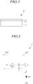
- FIG. 1 is a cross-sectional view illustrating an exemplary embodiment of an organic light emitting diode display device according to the present exemplary embodiment.
- an organic light emitting diode display device 100 may include a first substrate 110, an organic film 120 deposited on the first substrate 110 which emits light, and a second substrate 130 which protects the organic film 120 deposited on the first substrate 110.
- the second substrate 130 may be bonded to the first substrate 110 by a sealing material (not illustrated) to seal the organic film 120, and thus may be referred to as a sealing substrate.
- the first substrate 110 may include a plurality of pixel circuits (not illustrated) which selectively transmit a current to the organic film 120 to emit light in the organic film 120.
- the present disclosure is not limited thereto, and the first substrate 110 may be a substrate in which a plurality of pixel circuits are formed. In each of the pixel circuits, elements such as a plurality of transistors (not illustrated) and capacitors (not illustrated) may be formed.
- the first substrate 110 may be formed of an insulating material or a metal material.
- the organic film 120 may be included in an organic light emitting diode, and the organic light emitting diode may receive a driving current from the pixel circuit and emit light to a corresponding pixel.
- the organic film 120 may be an organic compound layer which is formed on an anode electrode of the organic light emitting diode and a cathode electrode of the organic light emitting diode and formed between the anode and cathode electrodes.
- the organic compound layer may include a hole injection layer (HIL), a hole transport layer (HTL), an emission layer (EML), an electron transport layer (ETL), and an electron injection layer (EIL).
- the second substrate 130 may face and be bonded to the first substrate 110 to protect the organic film 120 from moisture or foreign matter.
- the second substrate 130 may have a thickness of 5 ⁇ m or more, and may be formed of an insulating material.
- touch electrodes such as those illustrated in FIG. 3 may be disposed on the second substrate 130. That is, a separate touch panel is not formed on the second substrate 130, but the touch electrodes may be formed on the second substrate 130 so that the touch electrodes may be embedded in the display device.
- FIG. 2 is a circuit diagram illustrating an exemplary embodiment of a structure of a pixel used in the organic light emitting diode display device illustrated in FIG. 1 .
- the display device may include a plurality of pixels, and each of the pixels may include an organic light emitting diode OLED and a pixel circuit 101.
- the pixel circuit 101 may include first and second transistors M1 and M2 and a capacitor C1 and may control a current which flows in the organic light emitting diode OLED.
- the first transistor M1 may be a driving transistor for driving the current which flows in the organic light emitting diode OLED.
- a low potential voltage EVSS transmitted to a cathode electrode of the organic light emitting diode OLED may be a ground.
- the present disclosure is not limited thereto.
- a first electrode of the first transistor M1 may be connected to a high potential voltage line VL to which a high potential voltage EVDD is transmitted, a second electrode thereof may be connected to an anode electrode of the organic light emitting diode OLED, and a gate electrode thereof may be connected to a first node N1. Further, the first transistor M1 may drive a driving current in a direction from the first electrode to the second electrode according to a voltage difference between the first electrode and the gate electrode. The driving current may be transmitted to the organic light emitting diode OLED so that the organic light emitting diode OLED may emit light.
- a first electrode of the second transistor M2 may be connected to a data line DL to which a data voltage VDATA corresponding to a data signal is transmitted, a second electrode thereof may be connected to the first node N1, and a gate electrode thereof may be connected to a gate line S.
- the second transistor M2 may transmit the data voltage VDATA corresponding to a data signal, which is transmitted through the data line DL, to the first node N1 in response to a voltage of a gate signal transmitted through the gate line S.
- the capacitor C1 may be disposed to connect the first node N1 and a second node N2 and may maintain a voltage applied to the gate electrode of the first transistor M1 by maintaining a voltage between the first node N1 and the second node N2.
- the first electrodes of the first transistor M1 and the second transistor M2 may be drain electrodes, and the second electrodes thereof may be source electrodes.
- the present disclosure is not limited thereto.
- each of the transistors is illustrated as a p-channel metal-oxide semiconductor (PMOS) transistor, but the present disclosure is not limited thereto, and each of the transistors may be an n-channel metal-oxide semiconductor (NMOS) transistor.
- CMOS metal-oxide semiconductor
- a structure of the pixel circuit is only exemplary, but the present disclosure is not limited thereto.
- FIG. 3 is a plan view illustrating an exemplary embodiment of touch electrodes used in the organic light emitting diode display device according to the present exemplary embodiment.
- a plurality of touch electrodes TE may be disposed on a second substrate.
- the touch electrode TE may include a plurality of driving electrodes and a plurality of sensing electrodes. Further, a display device in which the touch electrodes TE are disposed may be divided into a plurality of areas, and the plurality of areas may include a first area 1301 and a third area 1303, which are disposed at an upper portion 130a of the display device based on a virtual central line X-X', and a second area 1302 and a fourth area 1304, which are disposed at a lower portion 130b of the display device. Further, a first driving electrode 131a may be disposed at a portion of the first area 1301, and a second driving electrode 131b may be disposed at a portion of the second area 1302.
- a third driving electrode 131c may be disposed at a portion of the third area 1303, and a fourth driving electrode 131d may be disposed at a portion of the fourth area 1304.
- a first sensing electrode 132a corresponding to the first driving electrode 131a may be disposed at another portion of the first area 1301, and a second sensing electrode 132b corresponding to the second driving electrode 131b may be disposed at another portion of the second area 1302.
- the first sensing electrode 132a disposed at the other portion of the first area 1301 may extend and may be disposed at another portion of the third area 1303, and the second sensing electrode 132b disposed at the other portion of the second area 1302 may extend and may be disposed at another portion of the fourth area 1304.
- first driving electrode 131a and the second driving electrode 131b may be connected by a first routing line 1311
- third driving electrode 131c and the fourth driving electrode 131d may be connected by the second routing line 1312. That is, a pair of driving electrodes may be connected to a single routing line.
- the second driving electrode 131b may be connected to a first driving line 1313 for transmitting a first driving signal
- the first driving electrode 131 a may receive the first driving signal through the first routing line 1311 transmitted to the second driving electrode 131b
- the fourth driving electrode 131d may be connected to a second driving line 1314 for transmitting a second driving signal
- the third driving electrode 131c may receive the second driving signal through the second routing line 1312 transmitted to the fourth driving electrode 131d through the second driving line 1314.
- a first sensing line 1121 may be connected to the first sensing electrode 132a
- a second sensing line 1322 may be connected to the second sensing electrode 132b.
- a driving line including the first driving line 1313 and the second driving line 1314 and a sensing line including the first sensing line 1121 and the second sensing line 1322 may be connected to a touch driver integrated circuit (IC) 350.
- IC touch driver integrated circuit
- the touch driver IC 350 may apply a driving signal to the driving line including the first driving line 1313 and the second driving line 1314, and may receive a sensing signal corresponding to the driving signal through the first sensing line 1121 and the second sensing line 1322.
- the touch driver IC 350 transmits a first driving signal to the second driving electrode 131b through the first driving line 1313, the first driving signal may be transmitted to the first driving electrode 131a connected to the second driving electrode 131b in a pair.
- the touch driver IC 350 transmits a second driving signal to the fourth driving electrode 131d through the second driving line 1314, the second driving signal may be transmitted to the third driving electrode 131c connected to the fourth driving electrode 131d in a pair.
- the sensing electrodes are divided into the first sensing electrode 132a and the second sensing electrode 132b in this way, two sensing signals corresponding to the driving signals transmitted in a pair may be output. By doing this, even when the number of driving signals applied to the driving electrodes is reduced, the sensing signals may be output to correspond to the number of driving electrodes. Therefore, the number of channels for outputting driving signals of the touch driver IC 350 may be reduced by half. By doing this, a time for which a driving signal is applied during a single touch sensing interval in the touch driver IC 350 may be reduced.
- FIG. 4 is a cross-sectional view illustrating an exemplary embodiment of the display device in which the touch electrodes illustrated in FIG. 3 are formed.
- a routing interconnection 4311, a first driving electrode 431, and a first sensing electrode 432 may be arranged on a second substrate 430 of the display device. That is, the first driving electrode 431 and the first sensing electrode 432 may be arranged in a single layer on the second substrate 430 rather than different layers thereon. That is, the routing interconnection 4311, the first driving electrode 431, and the first sensing electrode 432 may be formed by depositing and patterning a metal layer on a first insulating film. After the routing interconnection 4311, the first driving electrode 431, and the first sensing electrode 432 are patterned and formed, a second insulating film may be deposited thereon.
- routing interconnection 4311, the first driving electrode 431, and the first sensing electrode 432 may be formed by depositing and patterning the metal layer, the routing interconnection 4311, the first driving electrode 431, and the first sensing electrode 432 may be formed of the same metal. Therefore, a thinner display device than that in which the first driving electrode 431 and the first sensing electrode 432 are arranged in different layers may be implemented.
- FIG. 5A is a plan view illustrating an exemplary embodiment of the touch electrodes illustrated in FIG. 3
- FIG. 5B is a cross-sectional view illustrating the exemplary embodiment of the touch electrodes illustrated in FIG. 3 .
- an area B illustrated in FIG. 3 is illustrated.
- the area B represents an area in which opening areas having different sizes are formed in the touch electrode.
- the area B is illustrated as being in a portion of the third driving electrode 131c in FIG. 3 , but the present disclosure is not limited thereto, and the entire third driving electrode 131c may be formed as the area B and upper portions of the other driving electrodes and/or the other sensing electrodes may also have opening areas 510 as the area B.
- each touch electrode 500 may be formed of an opaque conductor, but light may be emitted by the opening areas 510 in the electrode.
- the opening areas 510 may include an opening area 510a for emitting red light, an opening area 510b for emitting green light, and an opening area 510c for emitting blue light.
- Light passing through each of the opening areas 510 may correspond to a light emitting area corresponding to an organic film of an organic light emitting diode included in each pixel, and the organic light emitting diode may emit any one of red light, green light, and blue light to the light emitting area.
- the organic light emitting diode which emits light through the opening area may emit white light
- color filters may be disposed in respective opening areas 510a, 510b, and 510c.
- the color filters may be formed to cover the opening areas or may be formed below the opening areas.
- the opening areas 510 may be implemented to have a predetermined size and may be formed to have different sizes depending on colors of light to be emitted. That is, a size of the opening area 510a from which red light is emitted and a size of the opening area 510b from which green light is emitted are greater than a size of the opening area 510c from which blue light is emitted, and thus it is possible to compensate for blue light having a low emission efficiency and a short life span.
- the present disclosure is not limited thereto.
- the touch electrodes 500 may be formed to have a predetermined thickness t1, and a dielectric 530 may be positioned below the touch electrodes 500 to have a predetermined thickness t2.
- an emission surface 520 for emitting light having a color from the opening area in which the touch electrode is not covered may be disposed below the dielectric 530.
- the emission surface 520 may correspond to an organic film of an organic light emitting diode and to an upper surface of a color filter.
- a size of the opening area may be greater than a size of the light emitting area of the organic light emitting diode, or may be greater than sizes of the color filters disposed below the opening areas 510a, 510b, and 510c.
- a gap d having a predetermined interval may be present between the touch electrode 500 and the light emitting area or the emission surface 520 corresponding to the upper surface of the color filter.
- the interval of the gap d may correspond to the sum of the thickness t1 of the touch electrode 500 and the thickness t2 of the dielectric 530. Further, the interval of the gap d may correspond to a half of the sum of the thickness t1 of the touch electrode 500 and the thickness t2 of the dielectric 530.
- the entire emission surface 520 exposed in the opening areas 510 may be visible to a user as seen in a front view of the display device, and by doing this, the color coordinates may not be distorted.
- an outer edge of the emission surface 520 exposed in the opening areas 510 is partially covered by the touch electrode 500 as seen in a side view having the predetermined angle ⁇ with a front view rather than in a front view of the display device, a portion of the emission surface 520 is not exposed to a user's view, and thus the user viewing the display device in a side view may recognize that color coordinates of an image are distorted.
- the size of the emission surface 520 is implemented to be smaller than the size of the opening area, since there is no portion covered by the touch electrode 500 in the light emitting area or the color filter even when the display device is viewed in a side view, it is possible to prevent a phenomenon in which color coordinates are distorted according to a viewing angle.
- the dielectric 530 may be a non-conductive material disposed between the light emitting area and/or the color filter and the touch electrode 500 disposed on the light emitting area and/or the color filter, and may be at least one of a passivation layer and an overcoating layer.
- the present disclosure is not limited thereto.
- FIG. 6 is a cross-sectional view illustrating another exemplary embodiment of the touch electrodes illustrated in FIG. 3 .
- a routing interconnection 6311 may be formed on a second substrate 630, and a passivation layer 6312 may be formed on the routing interconnection 6311.
- touch electrodes TE may be formed on the passivation layer 6312.
- the touch electrode TE may include a driving electrode and a sensing electrode.
- opening areas may be formed in the touch electrodes TE so that light emitted to a lower portion of the second substrate 630 may be emitted through the opening areas.
- an overcoating layer 6313 may be deposited on the second substrate 630 in which the touch electrodes TE are formed.
- a black matrix BM and color filters CF may be deposited on the deposited overcoating layer 6313. Since the touch electrodes including the driving electrodes and the sensing electrodes may be formed on the second substrate, that is, on the same layer, a thinner display device may be implemented.
- the color filters CF may be disposed on the touch electrodes and the color filters CF may not be covered by the touch electrodes, a problem due to a viewing angle may not occur. Further, since the black matrix BM is disposed to correspond to upper portions of the touch electrodes TE formed therebelow, an aperture ratio of the display device may be prevented from being reduced.
- FIG. 7 is a cross-sectional view illustrating still another exemplary embodiment of the touch electrodes illustrated in FIG. 3 .
- a black matrix BM and color filters CF may be disposed on a second substrate 730, an overcoating layer 7312 may be deposited on the black matrix BM and the color filters CF, and a metal layer may be formed and patterned on the overcoating layer 7312 to form a routing interconnection 7311. Further, after a passivation layer 7313 is deposited on the routing interconnection 7311 and an upper portion of the passivation layer 7313 is planarized, a metal layer may be deposited and patterned to form touch electrodes TE. Opening areas 740 may be formed in the touch electrodes TE. Here, the opening areas 740 are illustrated as having a predetermined interval, but the present disclosure is not limited thereto.
- routing interconnection 7311 and the touch electrodes TE may have the same material.
- the routing interconnection 7311 and the touch electrodes TE are illustrated as being disposed on different layers on the second substrate 730, but the routing interconnection 7311 and the touch electrodes TE are only exemplary and may be disposed on the same layer.
- a size of a color filter CF corresponding to a single pixel should be smaller than a size of the opening areas 740.
- FIG. 8 is a cross-sectional view illustrating yet another exemplary embodiment of the touch electrodes illustrated in FIG. 3 .
- a metal layer may be formed and patterned on a second substrate 830 to form a routing interconnection 8311. Further, after a passivation layer 8313 is deposited on the routing interconnection 8311 and an upper portion of the passivation layer 8313 is planarized, a metal layer may be deposited and patterned to form touch electrodes TE. Opening areas 840 may be formed in the touch electrodes TE. Here, the opening areas 840 are illustrated as having a predetermined interval, but the present disclosure is not limited thereto. Further, the metal layers which form the routing interconnection 8311 and the touch electrodes TE may have the same material. Here, the routing interconnection 8311 and the touch electrodes TE are illustrated as being disposed on different layers on the second substrate 830, but the routing interconnection 8311 and the touch electrodes TE are only exemplary and may be disposed on the same layer.
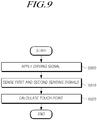
- FIG. 9 is a flowchart illustrating an exemplary embodiment of a touch sensing method of sensing a touch in an organic light emitting diode display device including the touch electrodes illustrated in FIG. 3 .
- the touch sensing method may include applying driving signals to a first driving electrode and a second driving electrode disposed in a first area and a second area of a display device which are different from each other.
- the first driving electrode and the second driving electrode may be connected in a pair, and a driving signal applied to the second driving electrode may be applied to the first driving electrode (S900). Therefore, even when a single driving signal is transmitted to a single driving electrode, two driving electrodes may receive the driving signal. Therefore, since the number of channels for outputting driving signals of the touch driver IC which outputs the driving signals may be reduced, a time for which a driving signal is applied to a plurality of driving electrodes during a single touch sensing interval may be reduced.
- a second driving signal may be applied to a third driving electrode and a fourth driving electrode, which are disposed in a third area adjacent to a first area of the display device and a fourth area adjacent to a second area.
- a first sensing signal corresponding to the driving signal applied to the first driving electrode may be sensed, and a second sensing signal corresponding to the driving signal applied to the second driving electrode may be sensed (S910).
- the first sensing electrode corresponds to the first driving electrode and the second sensing electrode corresponds to the second driving electrode, thereby outputting two sensing signals corresponding to a single driving signal.
- the sensing signals output from the sensing electrodes may be transmitted to the touch driver IC. Further, when the sensing signals are sensed, a third sensing signal corresponding to the second driving signal may be sensed from the first sensing electrode, and a fourth sensing signal corresponding to the second driving signal may be sensed from the second sensing electrode.
- touch points of the display device corresponding to the first sensing signal and the second sensing signal may be calculated (S920).
- the touch points may transmit the first sensing signal and the second sensing signal which are transmitted to the touch driver IC to a control-ler, and the controller may calculate information on the driving signals supplied to the touch driver IC and information included in the first sensing signal and the second sensing signal using a preset algorithm.
- the controller may be a specific controller for calculating a touch point and may be a timing controller for controlling the driving of the organic light emitting diode display device.
- the present disclosure is not limited thereto.
Abstract
Description
- This application claims priority from Korean Patent Application No.
10-2016-0127123 filed on September 30, 2016 - Exemplary embodiments of the present disclosure relate to an organic light emitting display device and a touch sensing method for the same.
- An organic light emitting display device is a display device which displays an image using organic light emitting diodes. The organic light emitting diode, which is a self-light-emitting element which emits light by itself, has a high response speed, high light emitting efficiency, high luminance, and a wide viewing angle.
- Further, a display device may operate by receiving a user's commands through various input devices such as a keyboard, a mouse, and the like, and thus input devices to which a user can intuitively and conveniently input commands by touching a screen of the display device are being developed. To this end, a touch panel is disposed on a screen of a display device and is touched by a user who views the screen of the display device, and thus the display device may receive the user's command. However, when the touch panel is disposed on the display device, the display device may become thick and heavy due to the touch panel and visibility may be reduced due to reduction of luminance. Further, recently, due to the spread of mobile devices and the beauty of their appearance, there are attempts to implement thinner and lighter display devices.
- Therefore, due to the above-described problem and recent trends, there are attempts to implement thinner display devices. To this end, a method of mounting a touch electrode on a display device through an additional process in a process of manufacturing the display device rather than a method of disposing a touch panel on the display device has been proposed.
- However, since the touch electrodes mounted on the display device include a plurality of capacitors formed by disposing a plurality of layers on the display device to dispose a plurality of driving electrode lines and a plurality of sensing electrode lines, a plurality of layers are required and there is a limit in minimizing, e.g. thinning down, the display device.
- Further, driving signals are sequentially transmitted to respective driving electrode lines when a touch point is calculated. However, when a size of the display device is large, there is a problem in that it takes a long time to transmit the driving signals to respective driving electrode lines.
- The above identified problems are solved by the features of the independent claims. Advantageous embodiments are derived from the dependent claims. The present disclosure has been made in an effort to provide an organic light emitting diode display device in which a thin thickness is implemented.
- The present disclosure has been made in an effort to provide a touch sensing method for an organic light emitting display device in which calculation of a touch point is performed more quickly.
- According to an exemplary embodiment (aspect) of the present disclosure, there is provided an organic light emitting display device. The organic light emitting display device includes a first driving electrode disposed on a portion of a first area of a (the) display device, a second driving electrode disposed on a portion of a second area of the display device and connected to the first driving electrode, a first sensing electrode disposed on another portion of the first area and configured to correspond to the first driving electrode, and a second sensing electrode disposed on another portion of the second area and configured to correspond to the second driving electrode.
- In an exemplary embodiment, the organic light emitting display device further comprises a third driving electrode disposed on a portion of a third area of the display device adjacent to the first area.
- In an exemplary embodiment, the first sensing electrode extends and is disposed on another portion of the third area.
- In an exemplary embodiment, the organic light emitting display device further comprises a fourth driving electrode disposed on a portion of a fourth area of the display device adjacent to the second area,
- In an exemplary embodiment, the second sensing electrode extends and is disposed on another portion of the fourth area.
- In an exemplary embodiment, a plurality of openings (opening areas) are formed in at least one electrode of the first driving electrode and the first sensing electrode.
- In an exemplary embodiment a color filter is disposed below the openings.
- In an exemplary embodiment, an emission surface is disposed in the openings.
- In an exemplary embodiment, the emission surface is disposed to have a predetermined interval from said at least one electrode in a horizontal direction.
- In an exemplary embodiment, the predetermined interval corresponds to a sum of a thickness of said at least one electrode and a distance from an upper surface of the emission surface to a lower surface of said at least one electrode.
- In an exemplary embodiment, a plurality of openings are formed in at least one electrode of the first driving electrode and the first sensing electrode.
- In an exemplary embodiment,the openings are covered by a color filter.
- In an exemplary embodiment, the first driving electrode and the first sensing electrode are disposed between a first film and a second film.
- According to an exemplary embodiment (aspect) of the present disclosure, there is provided an organic light emitting display device. The organic light emitting display device includes a display device, a driving electrode disposed on the display device and including a first driving electrode and a second driving electrode which are driven by a first driving signal, a sensing electrode disposed on the display device and including a first sensing electrode configured to correspond to the first driving electrode and output a first sensing signal corresponding to the first driving signal and a second sensing electrode configured to correspond to the second driving electrode and output a second sensing signal corresponding to the first driving signal, and a touch driver integrated circuit (IC) configured to transmit the first driving signal to the driving electrode and receive the first sensing signal and the second sensing signal from the sensing electrode.
- In an exemplary embodiment, the driving electrode further includes a third driving electrode adjacent to the first driving electrode and a fourth driving electrode adjacent to the second driving electrode, which are driven by a second driving signal, the first sensing electrode outputs a third sensing signal corresponding to the second driving signal, and the second sensing electrode outputs a fourth sensing signal corresponding to the second driving signal.
- In an exemplary embodiment, a plurality of openings are formed in at least one electrode of the first driving electrode and the first sensing electrode.
- In an exemplary embodiment, a color filter is disposed below the openings.
- In an exemplary embodiment, an emission surface is disposed in the openings, the emission surface is disposed to have a predetermined interval from said at least one electrode in a horizontal direction; and the predetermined interval corresponds to a sum of a thickness of said at least one electrode and a distance from an upper surface of the emission surface to a lower surface of said at least one electrode.
- In an exemplary embodiment, a plurality of openings are formed in at least one electrode of the first driving electrode and the first sensing electrode, and the openings are covered by a color filter.
- In an exemplary embodiment, the first driving electrode and the first sensing electrode are disposed between a first film and a second film.
- According to an exemplary embodiment of the present disclosure, there is provided a touch sensing method for an organic light emitting display device. The touch sensing method includes applying a first driving signal to a first driving electrode and a second driving electrode, which are disposed in a first area and a second area of a display device, sensing a first sensing signal from a first sensing electrode corresponding to a driving signal applied to the first driving electrode, and sensing a second sensing signal from a second sensing electrode corresponding to a driving signal applied to the second driving electrode, and calculating a touch point of the display device corresponding to the first sensing signal and the second sensing signal.
- In an exemplary embodiment. the applying of the first driving signal further includes applying a second driving signal to a third driving electrode and a fourth driving electrode which are disposed in a third area adjacent to the first area of the display device and a fourth area adjacent to the second area, and the sensing of the first and second sensing signals further includes sensing a third sensing signal from the first sensing electrode corresponding to the second driving signal and sensing a fourth sensing signal from the second sensing electrode corresponding to the second driving signal
- According to the exemplary embodiments of the present disclosure, an organic light emitting display device in which a thinner thickness is implemented can be provided.
- Further, a touch sensing method for an organic light emitting diode display device in which calculation of a touch point is performed more quickly by effectively transmitting a driving signal can be provided.
- The above and other aspects, features and advantages of the present disclosure will be more clearly understood from the following detailed description taken in conjunction with the accompanying drawings.
-
FIG. 1 is a cross-sectional view illustrating an exemplary embodiment of an organic light emitting display device according to the present exemplary embodiment. -
FIG. 2 is a circuit diagram illustrating an exemplary embodiment of a structure of a pixel used in the organic light emitting display device illustrated inFIG. 1 . -
FIG. 3 is a plan view illustrating an exemplary embodiment of touch electrodes used in the organic light emitting diode display device according to the present exemplary embodiment. -
FIG. 4 is a cross-sectional view illustrating an exemplary embodiment of a display device in which the touch electrodes illustrated inFIG. 3 are formed. -
FIG. 5A is a plan view illustrating an exemplary embodiment of the touch electrodes illustrated inFIG. 3 . -
FIG. 5B is a cross-sectional view illustrating an exemplary embodiment of the touch electrodes illustrated inFIG. 3 . -
FIG. 6 is a cross-sectional view illustrating another exemplary embodiment of the touch electrodes illustrated inFIG. 3 . -
FIG. 7 is a cross-sectional view illustrating still another exemplary embodiment of the touch electrodes illustrated inFIG. 3 . -
FIG. 8 is a cross-sectional view illustrating yet another exemplary embodiment of the touch electrodes illustrated inFIG. 3 . -
FIG. 9 is a flowchart illustrating an exemplary embodiment of a touch sensing method of sensing a touch in an organic light emitting display device including the touch electrodes illustrated inFIG. 3 . - Hereinafter, some exemplary embodiments of the present application will be described in detail with reference to the accompanying drawings. When reference numerals are assigned to components of each drawing, it should be noted that, even when the same components are illustrated in different drawings, the same numerals are assigned to the same components whenever possible. In addition, in descriptions of the present disclosure, when detailed descriptions of related well-known technology are deemed to unnecessarily obscure the gist of the disclosure, they will be omitted.
- Further, in describing components of the present disclosure, terminologies such as first, second, A, B, (a), and (b) may be used. These terms are only used to distinguish one component from another component, but the nature, order, or number of the corresponding components is not limited by these terms. It will be understood that when an element is referred to as being "connected" or "coupled" to another element, it can be directly connected or coupled to another element, intervening elements may be present, or it can be connected or coupled to another element through the other element.
-
FIG. 1 is a cross-sectional view illustrating an exemplary embodiment of an organic light emitting diode display device according to the present exemplary embodiment. - Referring to
FIG. 1 , an organic light emittingdiode display device 100 may include afirst substrate 110, anorganic film 120 deposited on thefirst substrate 110 which emits light, and asecond substrate 130 which protects theorganic film 120 deposited on thefirst substrate 110. Thesecond substrate 130 may be bonded to thefirst substrate 110 by a sealing material (not illustrated) to seal theorganic film 120, and thus may be referred to as a sealing substrate. - The
first substrate 110 may include a plurality of pixel circuits (not illustrated) which selectively transmit a current to theorganic film 120 to emit light in theorganic film 120. However, the present disclosure is not limited thereto, and thefirst substrate 110 may be a substrate in which a plurality of pixel circuits are formed. In each of the pixel circuits, elements such as a plurality of transistors (not illustrated) and capacitors (not illustrated) may be formed. Thefirst substrate 110 may be formed of an insulating material or a metal material. - The
organic film 120 may be included in an organic light emitting diode, and the organic light emitting diode may receive a driving current from the pixel circuit and emit light to a corresponding pixel. Theorganic film 120 may be an organic compound layer which is formed on an anode electrode of the organic light emitting diode and a cathode electrode of the organic light emitting diode and formed between the anode and cathode electrodes. The organic compound layer may include a hole injection layer (HIL), a hole transport layer (HTL), an emission layer (EML), an electron transport layer (ETL), and an electron injection layer (EIL). Further, when a driving voltage is applied to the anode electrode and the cathode electrode by an operation of a pixel circuit, holes which pass through the HTL and electrons which pass through the ETL move to the EML to form excitons, and as a result, visible light may be generated in the EML. - The
second substrate 130 may face and be bonded to thefirst substrate 110 to protect theorganic film 120 from moisture or foreign matter. Thesecond substrate 130 may have a thickness of 5 µm or more, and may be formed of an insulating material. Further, touch electrodes such as those illustrated inFIG. 3 may be disposed on thesecond substrate 130. That is, a separate touch panel is not formed on thesecond substrate 130, but the touch electrodes may be formed on thesecond substrate 130 so that the touch electrodes may be embedded in the display device. -
FIG. 2 is a circuit diagram illustrating an exemplary embodiment of a structure of a pixel used in the organic light emitting diode display device illustrated inFIG. 1 . - Referring to
FIG. 2 , the display device may include a plurality of pixels, and each of the pixels may include an organic light emitting diode OLED and apixel circuit 101. Thepixel circuit 101 may include first and second transistors M1 and M2 and a capacitor C1 and may control a current which flows in the organic light emitting diode OLED. Here, the first transistor M1 may be a driving transistor for driving the current which flows in the organic light emitting diode OLED. Further, a low potential voltage EVSS transmitted to a cathode electrode of the organic light emitting diode OLED may be a ground. However, the present disclosure is not limited thereto. - A first electrode of the first transistor M1 may be connected to a high potential voltage line VL to which a high potential voltage EVDD is transmitted, a second electrode thereof may be connected to an anode electrode of the organic light emitting diode OLED, and a gate electrode thereof may be connected to a first node N1. Further, the first transistor M1 may drive a driving current in a direction from the first electrode to the second electrode according to a voltage difference between the first electrode and the gate electrode. The driving current may be transmitted to the organic light emitting diode OLED so that the organic light emitting diode OLED may emit light.
- A first electrode of the second transistor M2 may be connected to a data line DL to which a data voltage VDATA corresponding to a data signal is transmitted, a second electrode thereof may be connected to the first node N1, and a gate electrode thereof may be connected to a gate line S. The second transistor M2 may transmit the data voltage VDATA corresponding to a data signal, which is transmitted through the data line DL, to the first node N1 in response to a voltage of a gate signal transmitted through the gate line S.
- The capacitor C1 may be disposed to connect the first node N1 and a second node N2 and may maintain a voltage applied to the gate electrode of the first transistor M1 by maintaining a voltage between the first node N1 and the second node N2.
- The first electrodes of the first transistor M1 and the second transistor M2 may be drain electrodes, and the second electrodes thereof may be source electrodes. However, the present disclosure is not limited thereto. Further, although each of the transistors is illustrated as a p-channel metal-oxide semiconductor (PMOS) transistor, but the present disclosure is not limited thereto, and each of the transistors may be an n-channel metal-oxide semiconductor (NMOS) transistor. Here, a structure of the pixel circuit is only exemplary, but the present disclosure is not limited thereto.
-
FIG. 3 is a plan view illustrating an exemplary embodiment of touch electrodes used in the organic light emitting diode display device according to the present exemplary embodiment. - Referring to
FIG. 3 , a plurality of touch electrodes TE may be disposed on a second substrate. - The touch electrode TE may include a plurality of driving electrodes and a plurality of sensing electrodes. Further, a display device in which the touch electrodes TE are disposed may be divided into a plurality of areas, and the plurality of areas may include a
first area 1301 and athird area 1303, which are disposed at anupper portion 130a of the display device based on a virtual central line X-X', and asecond area 1302 and afourth area 1304, which are disposed at alower portion 130b of the display device. Further, afirst driving electrode 131a may be disposed at a portion of thefirst area 1301, and asecond driving electrode 131b may be disposed at a portion of thesecond area 1302. Further, athird driving electrode 131c may be disposed at a portion of thethird area 1303, and afourth driving electrode 131d may be disposed at a portion of thefourth area 1304. Further, afirst sensing electrode 132a corresponding to thefirst driving electrode 131a may be disposed at another portion of thefirst area 1301, and asecond sensing electrode 132b corresponding to thesecond driving electrode 131b may be disposed at another portion of thesecond area 1302. Further, thefirst sensing electrode 132a disposed at the other portion of thefirst area 1301 may extend and may be disposed at another portion of thethird area 1303, and thesecond sensing electrode 132b disposed at the other portion of thesecond area 1302 may extend and may be disposed at another portion of thefourth area 1304. - Further, the
first driving electrode 131a and thesecond driving electrode 131b may be connected by afirst routing line 1311, and thethird driving electrode 131c and thefourth driving electrode 131d may be connected by thesecond routing line 1312. That is, a pair of driving electrodes may be connected to a single routing line. Further, thesecond driving electrode 131b may be connected to afirst driving line 1313 for transmitting a first driving signal, thefirst driving electrode 131 a may receive the first driving signal through thefirst routing line 1311 transmitted to thesecond driving electrode 131b, thefourth driving electrode 131d may be connected to asecond driving line 1314 for transmitting a second driving signal, and thethird driving electrode 131c may receive the second driving signal through thesecond routing line 1312 transmitted to thefourth driving electrode 131d through thesecond driving line 1314. Further, afirst sensing line 1121 may be connected to thefirst sensing electrode 132a, and asecond sensing line 1322 may be connected to thesecond sensing electrode 132b. Further, a driving line including thefirst driving line 1313 and thesecond driving line 1314 and a sensing line including thefirst sensing line 1121 and thesecond sensing line 1322 may be connected to a touch driver integrated circuit (IC) 350. - The
touch driver IC 350 may apply a driving signal to the driving line including thefirst driving line 1313 and thesecond driving line 1314, and may receive a sensing signal corresponding to the driving signal through thefirst sensing line 1121 and thesecond sensing line 1322. When thetouch driver IC 350 transmits a first driving signal to thesecond driving electrode 131b through thefirst driving line 1313, the first driving signal may be transmitted to thefirst driving electrode 131a connected to thesecond driving electrode 131b in a pair. Further, when thetouch driver IC 350 transmits a second driving signal to thefourth driving electrode 131d through thesecond driving line 1314, the second driving signal may be transmitted to thethird driving electrode 131c connected to thefourth driving electrode 131d in a pair. Since the sensing electrodes are divided into thefirst sensing electrode 132a and thesecond sensing electrode 132b in this way, two sensing signals corresponding to the driving signals transmitted in a pair may be output. By doing this, even when the number of driving signals applied to the driving electrodes is reduced, the sensing signals may be output to correspond to the number of driving electrodes. Therefore, the number of channels for outputting driving signals of thetouch driver IC 350 may be reduced by half. By doing this, a time for which a driving signal is applied during a single touch sensing interval in thetouch driver IC 350 may be reduced. -
FIG. 4 is a cross-sectional view illustrating an exemplary embodiment of the display device in which the touch electrodes illustrated inFIG. 3 are formed. - Referring to
FIG. 4 , arouting interconnection 4311, afirst driving electrode 431, and afirst sensing electrode 432 may be arranged on asecond substrate 430 of the display device. That is, thefirst driving electrode 431 and thefirst sensing electrode 432 may be arranged in a single layer on thesecond substrate 430 rather than different layers thereon. That is, therouting interconnection 4311, thefirst driving electrode 431, and thefirst sensing electrode 432 may be formed by depositing and patterning a metal layer on a first insulating film. After therouting interconnection 4311, thefirst driving electrode 431, and thefirst sensing electrode 432 are patterned and formed, a second insulating film may be deposited thereon. Since therouting interconnection 4311, thefirst driving electrode 431, and thefirst sensing electrode 432 may be formed by depositing and patterning the metal layer, therouting interconnection 4311, thefirst driving electrode 431, and thefirst sensing electrode 432 may be formed of the same metal. Therefore, a thinner display device than that in which thefirst driving electrode 431 and thefirst sensing electrode 432 are arranged in different layers may be implemented. -
FIG. 5A is a plan view illustrating an exemplary embodiment of the touch electrodes illustrated inFIG. 3 , andFIG. 5B is a cross-sectional view illustrating the exemplary embodiment of the touch electrodes illustrated inFIG. 3 . - Referring to
FIGS. 5A and 5B , an area B illustrated inFIG. 3 is illustrated. Here, the area B represents an area in which opening areas having different sizes are formed in the touch electrode. The area B is illustrated as being in a portion of thethird driving electrode 131c inFIG. 3 , but the present disclosure is not limited thereto, and the entirethird driving electrode 131c may be formed as the area B and upper portions of the other driving electrodes and/or the other sensing electrodes may also have openingareas 510 as the area B. - Therefore, each
touch electrode 500 may be formed of an opaque conductor, but light may be emitted by the openingareas 510 in the electrode. Further, the openingareas 510 may include anopening area 510a for emitting red light, anopening area 510b for emitting green light, and anopening area 510c for emitting blue light. Light passing through each of the openingareas 510 may correspond to a light emitting area corresponding to an organic film of an organic light emitting diode included in each pixel, and the organic light emitting diode may emit any one of red light, green light, and blue light to the light emitting area. Further, the organic light emitting diode which emits light through the opening area may emit white light, and color filters may be disposed inrespective opening areas areas 510 may be implemented to have a predetermined size and may be formed to have different sizes depending on colors of light to be emitted. That is, a size of theopening area 510a from which red light is emitted and a size of theopening area 510b from which green light is emitted are greater than a size of theopening area 510c from which blue light is emitted, and thus it is possible to compensate for blue light having a low emission efficiency and a short life span. However, the present disclosure is not limited thereto. - Further, as illustrated in
FIG. 5B , thetouch electrodes 500 may be formed to have a predetermined thickness t1, and a dielectric 530 may be positioned below thetouch electrodes 500 to have a predetermined thickness t2. Further, anemission surface 520 for emitting light having a color from the opening area in which the touch electrode is not covered may be disposed below the dielectric 530. Theemission surface 520 may correspond to an organic film of an organic light emitting diode and to an upper surface of a color filter. Further, a size of the opening area may be greater than a size of the light emitting area of the organic light emitting diode, or may be greater than sizes of the color filters disposed below the openingareas touch electrode 500 and the light emitting area or theemission surface 520 corresponding to the upper surface of the color filter. The interval of the gap d may correspond to the sum of the thickness t1 of thetouch electrode 500 and the thickness t2 of the dielectric 530. Further, the interval of the gap d may correspond to a half of the sum of the thickness t1 of thetouch electrode 500 and the thickness t2 of the dielectric 530. When a size of theemission surface 520 disposed below the dielectric 530 is the same as the size of the opening area, theentire emission surface 520 exposed in the openingareas 510 may be visible to a user as seen in a front view of the display device, and by doing this, the color coordinates may not be distorted. However, an outer edge of theemission surface 520 exposed in the openingareas 510 is partially covered by thetouch electrode 500 as seen in a side view having the predetermined angle θ with a front view rather than in a front view of the display device, a portion of theemission surface 520 is not exposed to a user's view, and thus the user viewing the display device in a side view may recognize that color coordinates of an image are distorted. However, when the size of theemission surface 520 is implemented to be smaller than the size of the opening area, since there is no portion covered by thetouch electrode 500 in the light emitting area or the color filter even when the display device is viewed in a side view, it is possible to prevent a phenomenon in which color coordinates are distorted according to a viewing angle. - Here, the dielectric 530 may be a non-conductive material disposed between the light emitting area and/or the color filter and the
touch electrode 500 disposed on the light emitting area and/or the color filter, and may be at least one of a passivation layer and an overcoating layer. However, the present disclosure is not limited thereto. -
FIG. 6 is a cross-sectional view illustrating another exemplary embodiment of the touch electrodes illustrated inFIG. 3 . - Referring to
FIG. 6 , arouting interconnection 6311 may be formed on asecond substrate 630, and apassivation layer 6312 may be formed on therouting interconnection 6311. Further, touch electrodes TE may be formed on thepassivation layer 6312. The touch electrode TE may include a driving electrode and a sensing electrode. Further, opening areas may be formed in the touch electrodes TE so that light emitted to a lower portion of thesecond substrate 630 may be emitted through the opening areas. Further, anovercoating layer 6313 may be deposited on thesecond substrate 630 in which the touch electrodes TE are formed. Further, a black matrix BM and color filters CF may be deposited on the depositedovercoating layer 6313. Since the touch electrodes including the driving electrodes and the sensing electrodes may be formed on the second substrate, that is, on the same layer, a thinner display device may be implemented. - In this case, since the color filters CF may be disposed on the touch electrodes and the color filters CF may not be covered by the touch electrodes, a problem due to a viewing angle may not occur. Further, since the black matrix BM is disposed to correspond to upper portions of the touch electrodes TE formed therebelow, an aperture ratio of the display device may be prevented from being reduced.
-
FIG. 7 is a cross-sectional view illustrating still another exemplary embodiment of the touch electrodes illustrated inFIG. 3 . - Referring to
FIG. 7 , a black matrix BM and color filters CF may be disposed on asecond substrate 730, anovercoating layer 7312 may be deposited on the black matrix BM and the color filters CF, and a metal layer may be formed and patterned on theovercoating layer 7312 to form arouting interconnection 7311. Further, after apassivation layer 7313 is deposited on therouting interconnection 7311 and an upper portion of thepassivation layer 7313 is planarized, a metal layer may be deposited and patterned to form touch electrodes TE.Opening areas 740 may be formed in the touch electrodes TE. Here, the openingareas 740 are illustrated as having a predetermined interval, but the present disclosure is not limited thereto. Further, the metal layers which form therouting interconnection 7311 and the touch electrodes TE may have the same material. Here, therouting interconnection 7311 and the touch electrodes TE are illustrated as being disposed on different layers on thesecond substrate 730, but therouting interconnection 7311 and the touch electrodes TE are only exemplary and may be disposed on the same layer. - In this case, since the color filters CF may be disposed below the touch electrodes TE, a size of a color filter CF corresponding to a single pixel should be smaller than a size of the
opening areas 740. -
FIG. 8 is a cross-sectional view illustrating yet another exemplary embodiment of the touch electrodes illustrated inFIG. 3 . - Referring to
FIG. 8 , a metal layer may be formed and patterned on asecond substrate 830 to form arouting interconnection 8311. Further, after apassivation layer 8313 is deposited on therouting interconnection 8311 and an upper portion of thepassivation layer 8313 is planarized, a metal layer may be deposited and patterned to form touch electrodes TE.Opening areas 840 may be formed in the touch electrodes TE. Here, the openingareas 840 are illustrated as having a predetermined interval, but the present disclosure is not limited thereto. Further, the metal layers which form therouting interconnection 8311 and the touch electrodes TE may have the same material. Here, therouting interconnection 8311 and the touch electrodes TE are illustrated as being disposed on different layers on thesecond substrate 830, but therouting interconnection 8311 and the touch electrodes TE are only exemplary and may be disposed on the same layer. -
FIG. 9 is a flowchart illustrating an exemplary embodiment of a touch sensing method of sensing a touch in an organic light emitting diode display device including the touch electrodes illustrated inFIG. 3 . - Referring to
FIG. 9 , the touch sensing method may include applying driving signals to a first driving electrode and a second driving electrode disposed in a first area and a second area of a display device which are different from each other. The first driving electrode and the second driving electrode may be connected in a pair, and a driving signal applied to the second driving electrode may be applied to the first driving electrode (S900). Therefore, even when a single driving signal is transmitted to a single driving electrode, two driving electrodes may receive the driving signal. Therefore, since the number of channels for outputting driving signals of the touch driver IC which outputs the driving signals may be reduced, a time for which a driving signal is applied to a plurality of driving electrodes during a single touch sensing interval may be reduced. Further, when the driving signal is applied to the driving electrode, a second driving signal may be applied to a third driving electrode and a fourth driving electrode, which are disposed in a third area adjacent to a first area of the display device and a fourth area adjacent to a second area. - Further, a first sensing signal corresponding to the driving signal applied to the first driving electrode may be sensed, and a second sensing signal corresponding to the driving signal applied to the second driving electrode may be sensed (S910). The first sensing electrode corresponds to the first driving electrode and the second sensing electrode corresponds to the second driving electrode, thereby outputting two sensing signals corresponding to a single driving signal. The sensing signals output from the sensing electrodes may be transmitted to the touch driver IC. Further, when the sensing signals are sensed, a third sensing signal corresponding to the second driving signal may be sensed from the first sensing electrode, and a fourth sensing signal corresponding to the second driving signal may be sensed from the second sensing electrode.
- Further, touch points of the display device corresponding to the first sensing signal and the second sensing signal may be calculated (S920). The touch points may transmit the first sensing signal and the second sensing signal which are transmitted to the touch driver IC to a control-ler, and the controller may calculate information on the driving signals supplied to the touch driver IC and information included in the first sensing signal and the second sensing signal using a preset algorithm. The controller may be a specific controller for calculating a touch point and may be a timing controller for controlling the driving of the organic light emitting diode display device. However, the present disclosure is not limited thereto.
- The above description is only an example describing the technological scope of the present disclosure. Various changes, modifications, and replacements may be made without departing from the scope of the present disclosure by those skilled in the field of display devices and touch sensing. Therefore, the exemplary embodiments disclosed above and in the accompanying drawings should be considered in a descriptive sense only and not for limiting the technological scope. The technological scope of the present disclosure is not limited by these embodiments or the accompanying drawings. The scope of the present disclosure should be interpreted by the appended claims and encompass all equivalents falling within the scope of the appended claims.
Claims (15)
- An organic light emitting display device (100) comprising:a first driving electrode (131a, 431) disposed on a portion of a first area (1301) of the display device (100);a second driving electrode (131b) disposed on a portion of a second area (1302) of the display device (100) and connected to the first driving electrode (131a, 431);a first sensing electrode (132a, 432) disposed on another portion of the first area (1301) and configured to correspond to the first driving electrode (131a, 431); anda second sensing electrode (132b) disposed on another portion of the second area (1302) and configured to correspond to the second driving electrode (131b).
- The organic light emitting display device (100) according to claim 1, further comprising:a third driving electrode (131c) disposed on a portion of a third area (1303) of the display device (100) adjacent to the first area (1301),wherein the first sensing electrode (132a, 432) extends and is disposed on another portion of the third area (1303).
- The organic light emitting display device (100) according to claim 2, further comprising:a fourth driving electrode (131d) disposed on a portion of a fourth area (1304) of the display device (100) adjacent to the second area (1302),wherein the second sensing electrode (132b) extends and is disposed on another portion of the fourth area (1304).
- The organic light emitting display device (100) according to one of the preceding claims, wherein a plurality of opening areas (510) are formed in at least one electrode of the first driving electrode (131a, 431) and the first sensing electrode (132a, 432).
- The organic light emitting display device (100) according to claim 4, wherein a color filter is disposed below the opening areas (510).
- The organic light emitting display device (100) according to claim 4 or 5, wherein an emission surface (520) is disposed in the opening areas (510).
- The organic light emitting display device (100) according to claim 6, wherein the emission surface (520) is disposed to have a predetermined interval from said at least one electrode in a horizontal direction.
- The organic light emitting display device (100) according to claim 6, wherein the predetermined interval corresponds to a sum of a thickness of said at least one electrode and a distance from an upper surface of the emission surface (520) to a lower surface of said at least one electrode.
- The organic light emitting display device (100) according to one of the preceding claims,
wherein a plurality of opening areas (510) are formed in at least one electrode of the first driving electrode (131a, 431) and the first sensing electrode (132a, 432). - The organic light emitting display device according to claim 9, wherein the opening areas (510) are covered by a color filter.
- The organic light emitting display device (100) according to one of the preceding claims, wherein the first driving electrode (131a, 431) and the first sensing electrode (132a, 432) are disposed between a first film and a second film.
- The organic light emitting display device (100) according to one of the preceding claims, wherein:a driving electrode disposed on the display device (100) and including the first driving electrode (131a, 431) and the second driving electrode (131b) which are driven by a first driving signal;a sensing electrode disposed on the display device (100) and including the first sensing electrode (132a, 432) configured to correspond to the first driving electrode (131a, 431) and output a first sensing signal corresponding to the first driving signal and the second sensing electrode (132b) configured to correspond to the second driving electrode (131b) and output a second sensing signal corresponding to the first driving signal; anda touch driver integrated circuit, IC, configured to transmit the first driving signal to the driving electrode and receive the first sensing signal and the second sensing signal from the sensing electrode.
- The organic light emitting display device (100) according to claim 12, wherein the driving electrode further includes the third driving electrode (131c) adjacent to the first driving electrode (131a, 431) and the fourth driving electrode (131d) adjacent to the second driving electrode (131b), which are driven by a second driving signal, the first sensing electrode (132a, 432) outputs a third sensing signal corresponding to the second driving signal, and the second sensing electrode (132b) outputs a fourth sensing signal corresponding to the second driving signal.
- A touch sensing method for an organic light emitting display device (100), the method comprising:applying a first driving signal to a first driving electrode (131a, 431) and a second driving electrode (131b) which are disposed in a first area (1301) and a second area (1302) of a display device (100);sensing a first sensing signal from a first sensing electrode (132a, 432) corresponding to a driving signal applied to the first driving electrode (131a, 431), and sensing a second sensing signal from a second sensing electrode (132b) corresponding to a driving signal applied to the second driving electrode (131b); andcalculating a touch point of the display device (100) corresponding to the first sensing signal and the second sensing signal.
- The touch sensing method for an organic light emitting display device (100) according to claim 14, wherein the applying of the first driving signal further includes applying a second driving signal to a third driving electrode (131c) and a fourth driving electrode (131d) which are disposed in a third area (1303) adjacent to the first area (1301) of the display device (100) and a fourth area (1304) adjacent to the second area (1302), and the sensing of the first and second sensing signals further includes sensing a third sensing signal from the first sensing electrode (132a, 432) corresponding to the second driving signal and sensing a fourth sensing signal from the second sensing electrode (132b) corresponding to the second driving signal.
Applications Claiming Priority (1)
| Application Number | Priority Date | Filing Date | Title |
|---|---|---|---|
| KR1020160127123A KR102567934B1 (en) | 2016-09-30 | 2016-09-30 | Organic light emitting display and touch senising method for the same |
Publications (2)
| Publication Number | Publication Date |
|---|---|
| EP3301552A1 true EP3301552A1 (en) | 2018-04-04 |
| EP3301552B1 EP3301552B1 (en) | 2021-11-17 |
Family
ID=57755083
Family Applications (1)
| Application Number | Title | Priority Date | Filing Date |
|---|---|---|---|
| EP16207514.7A Active EP3301552B1 (en) | 2016-09-30 | 2016-12-30 | Organic light emitting display device and touch sensing method for the same |
Country Status (6)
| Country | Link |
|---|---|
| US (1) | US10312297B2 (en) |
| EP (1) | EP3301552B1 (en) |
| JP (1) | JP6472431B2 (en) |
| KR (1) | KR102567934B1 (en) |
| CN (1) | CN107885378B (en) |
| TW (2) | TWI671664B (en) |
Cited By (2)
| Publication number | Priority date | Publication date | Assignee | Title |
|---|---|---|---|---|
| CN110162224A (en) * | 2018-05-31 | 2019-08-23 | 京东方科技集团股份有限公司 | Touch display substrate and its driving method, display device |
| EP3982417A1 (en) * | 2020-10-06 | 2022-04-13 | Samsung Display Co., Ltd. | Display device |
Families Citing this family (11)
| Publication number | Priority date | Publication date | Assignee | Title |
|---|---|---|---|---|
| KR102421678B1 (en) * | 2017-07-20 | 2022-07-19 | 삼성디스플레이 주식회사 | Touch sensor and display device having the same |
| JP6959065B2 (en) * | 2017-08-14 | 2021-11-02 | 株式会社ジャパンディスプレイ | Display device |
| KR102189017B1 (en) | 2019-01-17 | 2020-12-09 | 주식회사 하이딥 | Touch sensor panel and touch input apparatus |
| KR20200106589A (en) | 2019-03-04 | 2020-09-15 | 삼성디스플레이 주식회사 | Carrier, apparatus for manufacturing a display apparatus having the same and method for manufacturing a display apparatus |
| KR102256700B1 (en) * | 2019-03-26 | 2021-05-27 | 주식회사 하이딥 | Touch sensor panel |
| KR20210004006A (en) * | 2019-07-02 | 2021-01-13 | 삼성디스플레이 주식회사 | Display device |
| US11557635B2 (en) * | 2019-12-10 | 2023-01-17 | Samsung Display Co., Ltd. | Display device, mask assembly, and apparatus for manufacturing the display device |
| KR102402657B1 (en) * | 2020-05-19 | 2022-05-27 | 주식회사 티케이케미칼 | Fingerprint sensor integrated touch screen panel |
| KR20210151300A (en) | 2020-06-04 | 2021-12-14 | 삼성디스플레이 주식회사 | Display apparatus |
| KR20220006160A (en) | 2020-07-07 | 2022-01-17 | 삼성디스플레이 주식회사 | Display apparatus |
| KR20220016360A (en) | 2020-07-30 | 2022-02-09 | 삼성디스플레이 주식회사 | Input sensing panel and elecronic apparatus including the same |
Citations (4)
| Publication number | Priority date | Publication date | Assignee | Title |
|---|---|---|---|---|
| EP2148264A2 (en) * | 2008-07-21 | 2010-01-27 | Samsung Mobile Display Co., Ltd. | Organic light emitting display device |
| US20120168796A1 (en) * | 2010-12-30 | 2012-07-05 | Jung-Woo Moon | Light emitting diode display |
| CN103246422A (en) * | 2013-05-21 | 2013-08-14 | 敦泰科技有限公司 | Touch screen device and touch screen thereof |
| CN104035624A (en) * | 2014-06-30 | 2014-09-10 | 上海天马微电子有限公司 | Touch layer, touch panel, touch device, display panel and display device |
Family Cites Families (26)
| Publication number | Priority date | Publication date | Assignee | Title |
|---|---|---|---|---|
| JP3421078B2 (en) * | 1993-05-07 | 2003-06-30 | シャープ株式会社 | Information input / output device |
| CN101738761B (en) | 2008-11-26 | 2014-07-23 | 群创光电股份有限公司 | Touch panel |
| CN102289310B (en) | 2010-06-18 | 2014-07-02 | 胜华科技股份有限公司 | Touch display panel |
| US20120025516A1 (en) * | 2010-07-27 | 2012-02-02 | William John Miller | Secure Lottery Ticket Using Hybrid Construction |
| TWI401498B (en) | 2010-09-03 | 2013-07-11 | Au Optronics Corp | Flat display touch panel and fabricating method of the same |
| CN102985900B (en) * | 2011-02-24 | 2016-05-25 | 谱瑞科技股份有限公司 | single-layer touch sensor |
| TWI456321B (en) | 2011-12-08 | 2014-10-11 | Au Optronics Corp | Touch display panel |
| TWI567446B (en) | 2012-01-20 | 2017-01-21 | 群康科技(深圳)有限公司 | In-cell touch panel display |
| US9519810B2 (en) * | 2012-07-31 | 2016-12-13 | Datalogic ADC, Inc. | Calibration and self-test in automated data reading systems |
| CN103293735B (en) * | 2012-08-27 | 2015-11-25 | 上海天马微电子有限公司 | Touch control type LCD device |
| CN102830556B (en) | 2012-08-31 | 2015-08-19 | 北京京东方光电科技有限公司 | A kind of touch display panel and display device |
| KR20140059429A (en) * | 2012-11-08 | 2014-05-16 | 삼성전기주식회사 | Touch panel and method for manufacturing the same |
| US9354755B2 (en) * | 2012-11-27 | 2016-05-31 | Guardian Industries Corp. | Projected capacitive touch panel with a silver-inclusive transparent conducting layer(s) |
| TWI498797B (en) | 2012-12-13 | 2015-09-01 | Au Optronics Corp | Touch panel and touch display panel |
| US9298300B2 (en) | 2013-05-01 | 2016-03-29 | Apple Inc. | Displays with integrated touch and improved image pixel aperture |
| CN104182104A (en) * | 2013-05-27 | 2014-12-03 | 胜华科技股份有限公司 | Touch control panel |
| US20140347319A1 (en) * | 2013-05-27 | 2014-11-27 | Wintek Corporation | Touch panel |
| KR102216554B1 (en) * | 2014-03-14 | 2021-02-17 | 삼성디스플레이 주식회사 | Touch panel and display device comprising the same |
| US9658726B2 (en) * | 2014-07-10 | 2017-05-23 | Cypress Semiconductor Corporation | Single layer sensor pattern |
| WO2016140282A1 (en) | 2015-03-03 | 2016-09-09 | シャープ株式会社 | Display device equipped with touch sensor |
| CN104793825B (en) * | 2015-04-30 | 2018-04-20 | 京东方科技集团股份有限公司 | A kind of touch input equipment and touch display device |
| US10168844B2 (en) * | 2015-06-26 | 2019-01-01 | Samsung Display Co., Ltd. | Flexible display device |
| US9715304B2 (en) * | 2015-06-30 | 2017-07-25 | Synaptics Incorporated | Regular via pattern for sensor-based input device |
| CN115808825A (en) * | 2016-03-15 | 2023-03-17 | 株式会社半导体能源研究所 | Display device, module, and electronic apparatus |
| KR102533076B1 (en) * | 2016-05-26 | 2023-05-18 | 삼성디스플레이 주식회사 | Touch sensor |
| KR102629869B1 (en) * | 2016-09-27 | 2024-01-30 | 삼성디스플레이 주식회사 | Touch screen, display device having the same and driving method thereof |
-
2016
- 2016-09-30 KR KR1020160127123A patent/KR102567934B1/en active IP Right Grant
- 2016-12-27 US US15/391,772 patent/US10312297B2/en active Active
- 2016-12-27 JP JP2016253090A patent/JP6472431B2/en active Active
- 2016-12-28 TW TW107112811A patent/TWI671664B/en active
- 2016-12-28 CN CN201611235029.3A patent/CN107885378B/en active Active
- 2016-12-28 TW TW105143706A patent/TWI625657B/en active
- 2016-12-30 EP EP16207514.7A patent/EP3301552B1/en active Active
Patent Citations (4)
| Publication number | Priority date | Publication date | Assignee | Title |
|---|---|---|---|---|
| EP2148264A2 (en) * | 2008-07-21 | 2010-01-27 | Samsung Mobile Display Co., Ltd. | Organic light emitting display device |
| US20120168796A1 (en) * | 2010-12-30 | 2012-07-05 | Jung-Woo Moon | Light emitting diode display |
| CN103246422A (en) * | 2013-05-21 | 2013-08-14 | 敦泰科技有限公司 | Touch screen device and touch screen thereof |
| CN104035624A (en) * | 2014-06-30 | 2014-09-10 | 上海天马微电子有限公司 | Touch layer, touch panel, touch device, display panel and display device |
Cited By (4)
| Publication number | Priority date | Publication date | Assignee | Title |
|---|---|---|---|---|
| CN110162224A (en) * | 2018-05-31 | 2019-08-23 | 京东方科技集团股份有限公司 | Touch display substrate and its driving method, display device |
| CN110162224B (en) * | 2018-05-31 | 2021-01-26 | 京东方科技集团股份有限公司 | Touch display substrate, driving method thereof and display device |
| US11347360B2 (en) | 2018-05-31 | 2022-05-31 | Boe Technology Group Co., Ltd. | Touch display substrate and method for driving the same, display device |
| EP3982417A1 (en) * | 2020-10-06 | 2022-04-13 | Samsung Display Co., Ltd. | Display device |
Also Published As
| Publication number | Publication date |
|---|---|
| TWI671664B (en) | 2019-09-11 |
| KR102567934B1 (en) | 2023-08-18 |
| JP6472431B2 (en) | 2019-02-20 |
| US10312297B2 (en) | 2019-06-04 |
| TW201814459A (en) | 2018-04-16 |
| TW201830214A (en) | 2018-08-16 |
| TWI625657B (en) | 2018-06-01 |
| CN107885378A (en) | 2018-04-06 |
| JP2018060494A (en) | 2018-04-12 |
| KR20180036896A (en) | 2018-04-10 |
| US20180097038A1 (en) | 2018-04-05 |
| EP3301552B1 (en) | 2021-11-17 |
| CN107885378B (en) | 2021-02-26 |
Similar Documents
| Publication | Publication Date | Title |
|---|---|---|
| EP3301552A1 (en) | Organic light emitting display device and touch sensing method for the same | |
| US10761632B2 (en) | Display device with touch sensor for suppressing deterioration of image quality caused by capacitor in touch sensor unit and method for manufacturing same | |
| JP6623164B2 (en) | Organic light emitting diode display with bottom shield | |
| JP6457086B2 (en) | Organic light-emitting diode display with large aperture ratio | |
| US11075253B2 (en) | Organic light-emitting display device | |
| US9455304B2 (en) | Organic light-emitting diode display with white and blue diodes | |
| KR102449131B1 (en) | Organic light emitting display device | |
| US20170110521A1 (en) | Transparent display apparatus | |
| JP6932596B2 (en) | Organic EL display device | |
| KR102520708B1 (en) | Organic light-emitting display apparatus | |
| KR102392503B1 (en) | Organic light emitting display device | |
| US9070890B2 (en) | Pixel and organic light emitting display device having the same | |
| KR102394650B1 (en) | Organic light emitting display device | |
| KR102247825B1 (en) | Bottom Emission Type Organic Light Emission Diode Display Having Color Filters And Method For Manufacturing The Same | |
| KR20200009008A (en) | Display device and electronic device | |
| US20210126081A1 (en) | Organic light-emitting display apparatus | |
| KR102309842B1 (en) | Organic light emitting diode display and manufactucring method of the same | |
| JP2006284915A (en) | Display device and array substrate | |
| CN110021238B (en) | Display apparatus and image pickup apparatus | |
| KR102531139B1 (en) | Organic light emitting display and manufaturing method for the same | |
| KR20180049361A (en) | Organic light emitting display device | |
| KR102051660B1 (en) | Organic light emitting device, method of fabricating the same and organic light emitting display | |
| KR20230117010A (en) | Display apparatus | |
| KR20210038182A (en) | Organic light emitting display device | |
| KR20170043136A (en) | Organic light emitting diode display |
Legal Events
| Date | Code | Title | Description |
|---|---|---|---|
| PUAI | Public reference made under article 153(3) epc to a published international application that has entered the european phase |
Free format text: ORIGINAL CODE: 0009012 |
|
| STAA | Information on the status of an ep patent application or granted ep patent |
Free format text: STATUS: REQUEST FOR EXAMINATION WAS MADE |
|
| 17P | Request for examination filed |
Effective date: 20161230 |
|
| AK | Designated contracting states |
Kind code of ref document: A1 Designated state(s): AL AT BE BG CH CY CZ DE DK EE ES FI FR GB GR HR HU IE IS IT LI LT LU LV MC MK MT NL NO PL PT RO RS SE SI SK SM TR |
|
| AX | Request for extension of the european patent |
Extension state: BA ME |
|
| RBV | Designated contracting states (corrected) |
Designated state(s): AL AT BE BG CH CY CZ DE DK EE ES FI FR GB GR HR HU IE IS IT LI LT LU LV MC MK MT NL NO PL PT RO RS SE SI SK SM TR |
|
| STAA | Information on the status of an ep patent application or granted ep patent |
Free format text: STATUS: EXAMINATION IS IN PROGRESS |
|
| 17Q | First examination report despatched |
Effective date: 20200128 |
|
| STAA | Information on the status of an ep patent application or granted ep patent |
Free format text: STATUS: EXAMINATION IS IN PROGRESS |
|
| GRAP | Despatch of communication of intention to grant a patent |
Free format text: ORIGINAL CODE: EPIDOSNIGR1 |
|
| STAA | Information on the status of an ep patent application or granted ep patent |
Free format text: STATUS: GRANT OF PATENT IS INTENDED |
|
| INTG | Intention to grant announced |
Effective date: 20210702 |
|
| RIN1 | Information on inventor provided before grant (corrected) |
Inventor name: LEE, JAEGYUN Inventor name: JUNG, JIHYUN Inventor name: AN, SUCHANG Inventor name: KIM, SANGKYU Inventor name: GWON, HYANGMYOUNG Inventor name: LEE, YANGSIK |
|
| GRAS | Grant fee paid |
Free format text: ORIGINAL CODE: EPIDOSNIGR3 |
|
| GRAA | (expected) grant |
Free format text: ORIGINAL CODE: 0009210 |
|
| STAA | Information on the status of an ep patent application or granted ep patent |
Free format text: STATUS: THE PATENT HAS BEEN GRANTED |
|
| AK | Designated contracting states |
Kind code of ref document: B1 Designated state(s): AL AT BE BG CH CY CZ DE DK EE ES FI FR GB GR HR HU IE IS IT LI LT LU LV MC MK MT NL NO PL PT RO RS SE SI SK SM TR |
|
| REG | Reference to a national code |
Ref country code: GB Ref legal event code: FG4D |
|
| REG | Reference to a national code |
Ref country code: IE Ref legal event code: FG4D |
|
| REG | Reference to a national code |
Ref country code: DE Ref legal event code: R096 Ref document number: 602016066265 Country of ref document: DE |
|
| REG | Reference to a national code |
Ref country code: AT Ref legal event code: REF Ref document number: 1448604 Country of ref document: AT Kind code of ref document: T Effective date: 20211215 |
|
| REG | Reference to a national code |
Ref country code: LT Ref legal event code: MG9D |
|
| REG | Reference to a national code |
Ref country code: NL Ref legal event code: MP Effective date: 20211117 |
|
| REG | Reference to a national code |
Ref country code: AT Ref legal event code: MK05 Ref document number: 1448604 Country of ref document: AT Kind code of ref document: T Effective date: 20211117 |
|
| PG25 | Lapsed in a contracting state [announced via postgrant information from national office to epo] |
Ref country code: RS Free format text: LAPSE BECAUSE OF FAILURE TO SUBMIT A TRANSLATION OF THE DESCRIPTION OR TO PAY THE FEE WITHIN THE PRESCRIBED TIME-LIMIT Effective date: 20211117 Ref country code: LT Free format text: LAPSE BECAUSE OF FAILURE TO SUBMIT A TRANSLATION OF THE DESCRIPTION OR TO PAY THE FEE WITHIN THE PRESCRIBED TIME-LIMIT Effective date: 20211117 Ref country code: FI Free format text: LAPSE BECAUSE OF FAILURE TO SUBMIT A TRANSLATION OF THE DESCRIPTION OR TO PAY THE FEE WITHIN THE PRESCRIBED TIME-LIMIT Effective date: 20211117 Ref country code: BG Free format text: LAPSE BECAUSE OF FAILURE TO SUBMIT A TRANSLATION OF THE DESCRIPTION OR TO PAY THE FEE WITHIN THE PRESCRIBED TIME-LIMIT Effective date: 20220217 Ref country code: AT Free format text: LAPSE BECAUSE OF FAILURE TO SUBMIT A TRANSLATION OF THE DESCRIPTION OR TO PAY THE FEE WITHIN THE PRESCRIBED TIME-LIMIT Effective date: 20211117 |
|
| PG25 | Lapsed in a contracting state [announced via postgrant information from national office to epo] |
Ref country code: IS Free format text: LAPSE BECAUSE OF FAILURE TO SUBMIT A TRANSLATION OF THE DESCRIPTION OR TO PAY THE FEE WITHIN THE PRESCRIBED TIME-LIMIT Effective date: 20220317 Ref country code: SE Free format text: LAPSE BECAUSE OF FAILURE TO SUBMIT A TRANSLATION OF THE DESCRIPTION OR TO PAY THE FEE WITHIN THE PRESCRIBED TIME-LIMIT Effective date: 20211117 Ref country code: PT Free format text: LAPSE BECAUSE OF FAILURE TO SUBMIT A TRANSLATION OF THE DESCRIPTION OR TO PAY THE FEE WITHIN THE PRESCRIBED TIME-LIMIT Effective date: 20220317 Ref country code: PL Free format text: LAPSE BECAUSE OF FAILURE TO SUBMIT A TRANSLATION OF THE DESCRIPTION OR TO PAY THE FEE WITHIN THE PRESCRIBED TIME-LIMIT Effective date: 20211117 Ref country code: NO Free format text: LAPSE BECAUSE OF FAILURE TO SUBMIT A TRANSLATION OF THE DESCRIPTION OR TO PAY THE FEE WITHIN THE PRESCRIBED TIME-LIMIT Effective date: 20220217 Ref country code: NL Free format text: LAPSE BECAUSE OF FAILURE TO SUBMIT A TRANSLATION OF THE DESCRIPTION OR TO PAY THE FEE WITHIN THE PRESCRIBED TIME-LIMIT Effective date: 20211117 Ref country code: LV Free format text: LAPSE BECAUSE OF FAILURE TO SUBMIT A TRANSLATION OF THE DESCRIPTION OR TO PAY THE FEE WITHIN THE PRESCRIBED TIME-LIMIT Effective date: 20211117 Ref country code: HR Free format text: LAPSE BECAUSE OF FAILURE TO SUBMIT A TRANSLATION OF THE DESCRIPTION OR TO PAY THE FEE WITHIN THE PRESCRIBED TIME-LIMIT Effective date: 20211117 Ref country code: GR Free format text: LAPSE BECAUSE OF FAILURE TO SUBMIT A TRANSLATION OF THE DESCRIPTION OR TO PAY THE FEE WITHIN THE PRESCRIBED TIME-LIMIT Effective date: 20220218 Ref country code: ES Free format text: LAPSE BECAUSE OF FAILURE TO SUBMIT A TRANSLATION OF THE DESCRIPTION OR TO PAY THE FEE WITHIN THE PRESCRIBED TIME-LIMIT Effective date: 20211117 |
|
| PG25 | Lapsed in a contracting state [announced via postgrant information from national office to epo] |
Ref country code: SM Free format text: LAPSE BECAUSE OF FAILURE TO SUBMIT A TRANSLATION OF THE DESCRIPTION OR TO PAY THE FEE WITHIN THE PRESCRIBED TIME-LIMIT Effective date: 20211117 Ref country code: SK Free format text: LAPSE BECAUSE OF FAILURE TO SUBMIT A TRANSLATION OF THE DESCRIPTION OR TO PAY THE FEE WITHIN THE PRESCRIBED TIME-LIMIT Effective date: 20211117 Ref country code: RO Free format text: LAPSE BECAUSE OF FAILURE TO SUBMIT A TRANSLATION OF THE DESCRIPTION OR TO PAY THE FEE WITHIN THE PRESCRIBED TIME-LIMIT Effective date: 20211117 Ref country code: EE Free format text: LAPSE BECAUSE OF FAILURE TO SUBMIT A TRANSLATION OF THE DESCRIPTION OR TO PAY THE FEE WITHIN THE PRESCRIBED TIME-LIMIT Effective date: 20211117 Ref country code: DK Free format text: LAPSE BECAUSE OF FAILURE TO SUBMIT A TRANSLATION OF THE DESCRIPTION OR TO PAY THE FEE WITHIN THE PRESCRIBED TIME-LIMIT Effective date: 20211117 Ref country code: CZ Free format text: LAPSE BECAUSE OF FAILURE TO SUBMIT A TRANSLATION OF THE DESCRIPTION OR TO PAY THE FEE WITHIN THE PRESCRIBED TIME-LIMIT Effective date: 20211117 |
|
| REG | Reference to a national code |
Ref country code: CH Ref legal event code: PL |
|
| REG | Reference to a national code |
Ref country code: DE Ref legal event code: R097 Ref document number: 602016066265 Country of ref document: DE |
|
| PG25 | Lapsed in a contracting state [announced via postgrant information from national office to epo] |
Ref country code: MC Free format text: LAPSE BECAUSE OF FAILURE TO SUBMIT A TRANSLATION OF THE DESCRIPTION OR TO PAY THE FEE WITHIN THE PRESCRIBED TIME-LIMIT Effective date: 20211117 |
|
| PLBE | No opposition filed within time limit |
Free format text: ORIGINAL CODE: 0009261 |
|
| STAA | Information on the status of an ep patent application or granted ep patent |
Free format text: STATUS: NO OPPOSITION FILED WITHIN TIME LIMIT |
|
| REG | Reference to a national code |
Ref country code: BE Ref legal event code: MM Effective date: 20211231 |
|
| 26N | No opposition filed |
Effective date: 20220818 |
|
| PG25 | Lapsed in a contracting state [announced via postgrant information from national office to epo] |
Ref country code: LU Free format text: LAPSE BECAUSE OF NON-PAYMENT OF DUE FEES Effective date: 20211230 Ref country code: IE Free format text: LAPSE BECAUSE OF NON-PAYMENT OF DUE FEES Effective date: 20211230 Ref country code: AL Free format text: LAPSE BECAUSE OF FAILURE TO SUBMIT A TRANSLATION OF THE DESCRIPTION OR TO PAY THE FEE WITHIN THE PRESCRIBED TIME-LIMIT Effective date: 20211117 |
|
| PG25 | Lapsed in a contracting state [announced via postgrant information from national office to epo] |
Ref country code: SI Free format text: LAPSE BECAUSE OF FAILURE TO SUBMIT A TRANSLATION OF THE DESCRIPTION OR TO PAY THE FEE WITHIN THE PRESCRIBED TIME-LIMIT Effective date: 20211117 Ref country code: BE Free format text: LAPSE BECAUSE OF NON-PAYMENT OF DUE FEES Effective date: 20211231 |
|
| PG25 | Lapsed in a contracting state [announced via postgrant information from national office to epo] |
Ref country code: LI Free format text: LAPSE BECAUSE OF NON-PAYMENT OF DUE FEES Effective date: 20211231 Ref country code: CH Free format text: LAPSE BECAUSE OF NON-PAYMENT OF DUE FEES Effective date: 20211231 |
|
| PG25 | Lapsed in a contracting state [announced via postgrant information from national office to epo] |
Ref country code: IT Free format text: LAPSE BECAUSE OF FAILURE TO SUBMIT A TRANSLATION OF THE DESCRIPTION OR TO PAY THE FEE WITHIN THE PRESCRIBED TIME-LIMIT Effective date: 20211117 Ref country code: HU Free format text: LAPSE BECAUSE OF FAILURE TO SUBMIT A TRANSLATION OF THE DESCRIPTION OR TO PAY THE FEE WITHIN THE PRESCRIBED TIME-LIMIT; INVALID AB INITIO Effective date: 20161230 |
|
| PG25 | Lapsed in a contracting state [announced via postgrant information from national office to epo] |
Ref country code: CY Free format text: LAPSE BECAUSE OF FAILURE TO SUBMIT A TRANSLATION OF THE DESCRIPTION OR TO PAY THE FEE WITHIN THE PRESCRIBED TIME-LIMIT Effective date: 20211117 |
|
| PGFP | Annual fee paid to national office [announced via postgrant information from national office to epo] |
Ref country code: GB Payment date: 20231023 Year of fee payment: 8 |
|
| PGFP | Annual fee paid to national office [announced via postgrant information from national office to epo] |
Ref country code: FR Payment date: 20231024 Year of fee payment: 8 Ref country code: DE Payment date: 20231023 Year of fee payment: 8 |