JP6932596B2 - Organic EL display device - Google Patents
Organic EL display device Download PDFInfo
- Publication number
- JP6932596B2 JP6932596B2 JP2017183510A JP2017183510A JP6932596B2 JP 6932596 B2 JP6932596 B2 JP 6932596B2 JP 2017183510 A JP2017183510 A JP 2017183510A JP 2017183510 A JP2017183510 A JP 2017183510A JP 6932596 B2 JP6932596 B2 JP 6932596B2
- Authority
- JP
- Japan
- Prior art keywords
- pixel
- electrode
- sub
- display device
- pixel electrode
- Prior art date
- Legal status (The legal status is an assumption and is not a legal conclusion. Google has not performed a legal analysis and makes no representation as to the accuracy of the status listed.)
- Active
Links
- 239000010410 layer Substances 0.000 claims description 44
- 239000000758 substrate Substances 0.000 claims description 19
- 239000002346 layers by function Substances 0.000 claims description 10
- XUIMIQQOPSSXEZ-UHFFFAOYSA-N Silicon Chemical compound [Si] XUIMIQQOPSSXEZ-UHFFFAOYSA-N 0.000 claims description 4
- 230000003287 optical effect Effects 0.000 claims description 4
- 239000010703 silicon Substances 0.000 claims description 4
- 229910052710 silicon Inorganic materials 0.000 claims description 4
- 230000005540 biological transmission Effects 0.000 claims description 2
- 238000000034 method Methods 0.000 description 16
- 239000003086 colorant Substances 0.000 description 5
- 239000011347 resin Substances 0.000 description 5
- 229920005989 resin Polymers 0.000 description 5
- 238000002347 injection Methods 0.000 description 4
- 239000007924 injection Substances 0.000 description 4
- 239000000463 material Substances 0.000 description 4
- 238000000926 separation method Methods 0.000 description 4
- 239000011230 binding agent Substances 0.000 description 3
- 238000000576 coating method Methods 0.000 description 3
- 230000000694 effects Effects 0.000 description 3
- 239000010408 film Substances 0.000 description 3
- 238000012905 input function Methods 0.000 description 3
- 229910052751 metal Inorganic materials 0.000 description 3
- 239000002184 metal Substances 0.000 description 3
- 239000000126 substance Substances 0.000 description 3
- PXHVJJICTQNCMI-UHFFFAOYSA-N Nickel Chemical compound [Ni] PXHVJJICTQNCMI-UHFFFAOYSA-N 0.000 description 2
- KDLHZDBZIXYQEI-UHFFFAOYSA-N Palladium Chemical compound [Pd] KDLHZDBZIXYQEI-UHFFFAOYSA-N 0.000 description 2
- RTAQQCXQSZGOHL-UHFFFAOYSA-N Titanium Chemical compound [Ti] RTAQQCXQSZGOHL-UHFFFAOYSA-N 0.000 description 2
- XLOMVQKBTHCTTD-UHFFFAOYSA-N Zinc monoxide Chemical compound [Zn]=O XLOMVQKBTHCTTD-UHFFFAOYSA-N 0.000 description 2
- 229910045601 alloy Inorganic materials 0.000 description 2
- 239000000956 alloy Substances 0.000 description 2
- 229910052782 aluminium Inorganic materials 0.000 description 2
- XAGFODPZIPBFFR-UHFFFAOYSA-N aluminium Chemical compound [Al] XAGFODPZIPBFFR-UHFFFAOYSA-N 0.000 description 2
- 230000000903 blocking effect Effects 0.000 description 2
- 239000000470 constituent Substances 0.000 description 2
- 238000010586 diagram Methods 0.000 description 2
- 238000001035 drying Methods 0.000 description 2
- 239000000284 extract Substances 0.000 description 2
- 239000011521 glass Substances 0.000 description 2
- AMGQUBHHOARCQH-UHFFFAOYSA-N indium;oxotin Chemical compound [In].[Sn]=O AMGQUBHHOARCQH-UHFFFAOYSA-N 0.000 description 2
- 239000004973 liquid crystal related substance Substances 0.000 description 2
- 239000011159 matrix material Substances 0.000 description 2
- 229910044991 metal oxide Inorganic materials 0.000 description 2
- 150000004706 metal oxides Chemical class 0.000 description 2
- 150000002739 metals Chemical class 0.000 description 2
- 238000010422 painting Methods 0.000 description 2
- BASFCYQUMIYNBI-UHFFFAOYSA-N platinum Chemical compound [Pt] BASFCYQUMIYNBI-UHFFFAOYSA-N 0.000 description 2
- 229920001721 polyimide Polymers 0.000 description 2
- 229910052709 silver Inorganic materials 0.000 description 2
- 239000004332 silver Substances 0.000 description 2
- 239000010936 titanium Substances 0.000 description 2
- 229910052719 titanium Inorganic materials 0.000 description 2
- 238000007740 vapor deposition Methods 0.000 description 2
- XLYOFNOQVPJJNP-UHFFFAOYSA-N water Substances O XLYOFNOQVPJJNP-UHFFFAOYSA-N 0.000 description 2
- 229920000178 Acrylic resin Polymers 0.000 description 1
- 239000004925 Acrylic resin Substances 0.000 description 1
- 229910001148 Al-Li alloy Inorganic materials 0.000 description 1
- OYPRJOBELJOOCE-UHFFFAOYSA-N Calcium Chemical compound [Ca] OYPRJOBELJOOCE-UHFFFAOYSA-N 0.000 description 1
- VYZAMTAEIAYCRO-UHFFFAOYSA-N Chromium Chemical compound [Cr] VYZAMTAEIAYCRO-UHFFFAOYSA-N 0.000 description 1
- RYGMFSIKBFXOCR-UHFFFAOYSA-N Copper Chemical compound [Cu] RYGMFSIKBFXOCR-UHFFFAOYSA-N 0.000 description 1
- WHXSMMKQMYFTQS-UHFFFAOYSA-N Lithium Chemical compound [Li] WHXSMMKQMYFTQS-UHFFFAOYSA-N 0.000 description 1
- 239000004642 Polyimide Substances 0.000 description 1
- BUGBHKTXTAQXES-UHFFFAOYSA-N Selenium Chemical compound [Se] BUGBHKTXTAQXES-UHFFFAOYSA-N 0.000 description 1
- BQCADISMDOOEFD-UHFFFAOYSA-N Silver Chemical compound [Ag] BQCADISMDOOEFD-UHFFFAOYSA-N 0.000 description 1
- 229920001807 Urea-formaldehyde Polymers 0.000 description 1
- JFBZPFYRPYOZCQ-UHFFFAOYSA-N [Li].[Al] Chemical compound [Li].[Al] JFBZPFYRPYOZCQ-UHFFFAOYSA-N 0.000 description 1
- 229920000122 acrylonitrile butadiene styrene Polymers 0.000 description 1
- 239000000654 additive Substances 0.000 description 1
- 229910052783 alkali metal Inorganic materials 0.000 description 1
- 150000001340 alkali metals Chemical class 0.000 description 1
- 229910052784 alkaline earth metal Inorganic materials 0.000 description 1
- 150000001342 alkaline earth metals Chemical class 0.000 description 1
- SNAAJJQQZSMGQD-UHFFFAOYSA-N aluminum magnesium Chemical compound [Mg].[Al] SNAAJJQQZSMGQD-UHFFFAOYSA-N 0.000 description 1
- 239000003963 antioxidant agent Substances 0.000 description 1
- 230000003078 antioxidant effect Effects 0.000 description 1
- -1 calcium Chemical compound 0.000 description 1
- 229910052791 calcium Inorganic materials 0.000 description 1
- 239000011575 calcium Substances 0.000 description 1
- 238000005266 casting Methods 0.000 description 1
- 229910052804 chromium Inorganic materials 0.000 description 1
- 239000011651 chromium Substances 0.000 description 1
- 229910017052 cobalt Inorganic materials 0.000 description 1
- 239000010941 cobalt Substances 0.000 description 1
- GUTLYIVDDKVIGB-UHFFFAOYSA-N cobalt atom Chemical compound [Co] GUTLYIVDDKVIGB-UHFFFAOYSA-N 0.000 description 1
- 229920001940 conductive polymer Polymers 0.000 description 1
- 229920001577 copolymer Polymers 0.000 description 1
- 229910052802 copper Inorganic materials 0.000 description 1
- 239000010949 copper Substances 0.000 description 1
- 238000002425 crystallisation Methods 0.000 description 1
- 230000008025 crystallization Effects 0.000 description 1
- 238000000151 deposition Methods 0.000 description 1
- 238000007598 dipping method Methods 0.000 description 1
- 238000005401 electroluminescence Methods 0.000 description 1
- 239000003822 epoxy resin Substances 0.000 description 1
- PCHJSUWPFVWCPO-UHFFFAOYSA-N gold Chemical compound [Au] PCHJSUWPFVWCPO-UHFFFAOYSA-N 0.000 description 1
- 229910052737 gold Inorganic materials 0.000 description 1
- 239000010931 gold Substances 0.000 description 1
- 230000005525 hole transport Effects 0.000 description 1
- 229920001519 homopolymer Polymers 0.000 description 1
- 238000003384 imaging method Methods 0.000 description 1
- 229910003437 indium oxide Inorganic materials 0.000 description 1
- PJXISJQVUVHSOJ-UHFFFAOYSA-N indium(iii) oxide Chemical compound [O-2].[O-2].[O-2].[In+3].[In+3] PJXISJQVUVHSOJ-UHFFFAOYSA-N 0.000 description 1
- 230000010365 information processing Effects 0.000 description 1
- 150000002484 inorganic compounds Chemical class 0.000 description 1
- 229910010272 inorganic material Inorganic materials 0.000 description 1
- 238000009413 insulation Methods 0.000 description 1
- 239000011133 lead Substances 0.000 description 1
- 229910052744 lithium Inorganic materials 0.000 description 1
- SJCKRGFTWFGHGZ-UHFFFAOYSA-N magnesium silver Chemical compound [Mg].[Ag] SJCKRGFTWFGHGZ-UHFFFAOYSA-N 0.000 description 1
- WPBNNNQJVZRUHP-UHFFFAOYSA-L manganese(2+);methyl n-[[2-(methoxycarbonylcarbamothioylamino)phenyl]carbamothioyl]carbamate;n-[2-(sulfidocarbothioylamino)ethyl]carbamodithioate Chemical compound [Mn+2].[S-]C(=S)NCCNC([S-])=S.COC(=O)NC(=S)NC1=CC=CC=C1NC(=S)NC(=O)OC WPBNNNQJVZRUHP-UHFFFAOYSA-L 0.000 description 1
- 239000000203 mixture Substances 0.000 description 1
- 229910052759 nickel Inorganic materials 0.000 description 1
- 150000002894 organic compounds Chemical class 0.000 description 1
- 239000012044 organic layer Substances 0.000 description 1
- 229910052763 palladium Inorganic materials 0.000 description 1
- 239000005011 phenolic resin Substances 0.000 description 1
- 239000004014 plasticizer Substances 0.000 description 1
- 229910052697 platinum Inorganic materials 0.000 description 1
- 229920003227 poly(N-vinyl carbazole) Polymers 0.000 description 1
- 229920000767 polyaniline Polymers 0.000 description 1
- 239000004417 polycarbonate Substances 0.000 description 1
- 229920005668 polycarbonate resin Polymers 0.000 description 1
- 239000004431 polycarbonate resin Substances 0.000 description 1
- 229920000647 polyepoxide Polymers 0.000 description 1
- 229920001225 polyester resin Polymers 0.000 description 1
- 239000004645 polyester resin Substances 0.000 description 1
- 239000009719 polyimide resin Substances 0.000 description 1
- 229920000128 polypyrrole Polymers 0.000 description 1
- 229920000123 polythiophene Polymers 0.000 description 1
- 238000002310 reflectometry Methods 0.000 description 1
- 229910052711 selenium Inorganic materials 0.000 description 1
- 239000011669 selenium Substances 0.000 description 1
- 239000002356 single layer Substances 0.000 description 1
- 239000000243 solution Substances 0.000 description 1
- 239000002904 solvent Substances 0.000 description 1
- 238000004528 spin coating Methods 0.000 description 1
- 238000004544 sputter deposition Methods 0.000 description 1
- 239000010409 thin film Substances 0.000 description 1
- XOLBLPGZBRYERU-UHFFFAOYSA-N tin dioxide Chemical compound O=[Sn]=O XOLBLPGZBRYERU-UHFFFAOYSA-N 0.000 description 1
- 229910001887 tin oxide Inorganic materials 0.000 description 1
- WFKWXMTUELFFGS-UHFFFAOYSA-N tungsten Chemical compound [W] WFKWXMTUELFFGS-UHFFFAOYSA-N 0.000 description 1
- 229910052721 tungsten Inorganic materials 0.000 description 1
- 239000010937 tungsten Substances 0.000 description 1
- 239000006097 ultraviolet radiation absorber Substances 0.000 description 1
- 238000001771 vacuum deposition Methods 0.000 description 1
- 229910052720 vanadium Inorganic materials 0.000 description 1
- GPPXJZIENCGNKB-UHFFFAOYSA-N vanadium Chemical compound [V]#[V] GPPXJZIENCGNKB-UHFFFAOYSA-N 0.000 description 1
- YVTHLONGBIQYBO-UHFFFAOYSA-N zinc indium(3+) oxygen(2-) Chemical compound [O--].[Zn++].[In+3] YVTHLONGBIQYBO-UHFFFAOYSA-N 0.000 description 1
- 239000011787 zinc oxide Substances 0.000 description 1
Images


Classifications
-
- G—PHYSICS
- G09—EDUCATION; CRYPTOGRAPHY; DISPLAY; ADVERTISING; SEALS
- G09G—ARRANGEMENTS OR CIRCUITS FOR CONTROL OF INDICATING DEVICES USING STATIC MEANS TO PRESENT VARIABLE INFORMATION
- G09G3/00—Control arrangements or circuits, of interest only in connection with visual indicators other than cathode-ray tubes
- G09G3/20—Control arrangements or circuits, of interest only in connection with visual indicators other than cathode-ray tubes for presentation of an assembly of a number of characters, e.g. a page, by composing the assembly by combination of individual elements arranged in a matrix no fixed position being assigned to or needed to be assigned to the individual characters or partial characters
- G09G3/22—Control arrangements or circuits, of interest only in connection with visual indicators other than cathode-ray tubes for presentation of an assembly of a number of characters, e.g. a page, by composing the assembly by combination of individual elements arranged in a matrix no fixed position being assigned to or needed to be assigned to the individual characters or partial characters using controlled light sources
- G09G3/30—Control arrangements or circuits, of interest only in connection with visual indicators other than cathode-ray tubes for presentation of an assembly of a number of characters, e.g. a page, by composing the assembly by combination of individual elements arranged in a matrix no fixed position being assigned to or needed to be assigned to the individual characters or partial characters using controlled light sources using electroluminescent panels
- G09G3/32—Control arrangements or circuits, of interest only in connection with visual indicators other than cathode-ray tubes for presentation of an assembly of a number of characters, e.g. a page, by composing the assembly by combination of individual elements arranged in a matrix no fixed position being assigned to or needed to be assigned to the individual characters or partial characters using controlled light sources using electroluminescent panels semiconductive, e.g. using light-emitting diodes [LED]
- G09G3/3208—Control arrangements or circuits, of interest only in connection with visual indicators other than cathode-ray tubes for presentation of an assembly of a number of characters, e.g. a page, by composing the assembly by combination of individual elements arranged in a matrix no fixed position being assigned to or needed to be assigned to the individual characters or partial characters using controlled light sources using electroluminescent panels semiconductive, e.g. using light-emitting diodes [LED] organic, e.g. using organic light-emitting diodes [OLED]
- G09G3/3225—Control arrangements or circuits, of interest only in connection with visual indicators other than cathode-ray tubes for presentation of an assembly of a number of characters, e.g. a page, by composing the assembly by combination of individual elements arranged in a matrix no fixed position being assigned to or needed to be assigned to the individual characters or partial characters using controlled light sources using electroluminescent panels semiconductive, e.g. using light-emitting diodes [LED] organic, e.g. using organic light-emitting diodes [OLED] using an active matrix
- G09G3/3233—Control arrangements or circuits, of interest only in connection with visual indicators other than cathode-ray tubes for presentation of an assembly of a number of characters, e.g. a page, by composing the assembly by combination of individual elements arranged in a matrix no fixed position being assigned to or needed to be assigned to the individual characters or partial characters using controlled light sources using electroluminescent panels semiconductive, e.g. using light-emitting diodes [LED] organic, e.g. using organic light-emitting diodes [OLED] using an active matrix with pixel circuitry controlling the current through the light-emitting element
-
- G—PHYSICS
- G09—EDUCATION; CRYPTOGRAPHY; DISPLAY; ADVERTISING; SEALS
- G09G—ARRANGEMENTS OR CIRCUITS FOR CONTROL OF INDICATING DEVICES USING STATIC MEANS TO PRESENT VARIABLE INFORMATION
- G09G3/00—Control arrangements or circuits, of interest only in connection with visual indicators other than cathode-ray tubes
- G09G3/20—Control arrangements or circuits, of interest only in connection with visual indicators other than cathode-ray tubes for presentation of an assembly of a number of characters, e.g. a page, by composing the assembly by combination of individual elements arranged in a matrix no fixed position being assigned to or needed to be assigned to the individual characters or partial characters
- G09G3/2007—Display of intermediate tones
- G09G3/2074—Display of intermediate tones using sub-pixels
-
- G—PHYSICS
- G09—EDUCATION; CRYPTOGRAPHY; DISPLAY; ADVERTISING; SEALS
- G09G—ARRANGEMENTS OR CIRCUITS FOR CONTROL OF INDICATING DEVICES USING STATIC MEANS TO PRESENT VARIABLE INFORMATION
- G09G2300/00—Aspects of the constitution of display devices
- G09G2300/04—Structural and physical details of display devices
- G09G2300/0439—Pixel structures
- G09G2300/0452—Details of colour pixel setup, e.g. pixel composed of a red, a blue and two green components
-
- G—PHYSICS
- G09—EDUCATION; CRYPTOGRAPHY; DISPLAY; ADVERTISING; SEALS
- G09G—ARRANGEMENTS OR CIRCUITS FOR CONTROL OF INDICATING DEVICES USING STATIC MEANS TO PRESENT VARIABLE INFORMATION
- G09G2300/00—Aspects of the constitution of display devices
- G09G2300/04—Structural and physical details of display devices
- G09G2300/0439—Pixel structures
- G09G2300/0456—Pixel structures with a reflective area and a transmissive area combined in one pixel, such as in transflectance pixels
-
- G—PHYSICS
- G09—EDUCATION; CRYPTOGRAPHY; DISPLAY; ADVERTISING; SEALS
- G09G—ARRANGEMENTS OR CIRCUITS FOR CONTROL OF INDICATING DEVICES USING STATIC MEANS TO PRESENT VARIABLE INFORMATION
- G09G2300/00—Aspects of the constitution of display devices
- G09G2300/08—Active matrix structure, i.e. with use of active elements, inclusive of non-linear two terminal elements, in the pixels together with light emitting or modulating elements
- G09G2300/0809—Several active elements per pixel in active matrix panels
- G09G2300/0842—Several active elements per pixel in active matrix panels forming a memory circuit, e.g. a dynamic memory with one capacitor
- G09G2300/0852—Several active elements per pixel in active matrix panels forming a memory circuit, e.g. a dynamic memory with one capacitor being a dynamic memory with more than one capacitor
-
- G—PHYSICS
- G09—EDUCATION; CRYPTOGRAPHY; DISPLAY; ADVERTISING; SEALS
- G09G—ARRANGEMENTS OR CIRCUITS FOR CONTROL OF INDICATING DEVICES USING STATIC MEANS TO PRESENT VARIABLE INFORMATION
- G09G2310/00—Command of the display device
- G09G2310/02—Addressing, scanning or driving the display screen or processing steps related thereto
- G09G2310/0262—The addressing of the pixel, in a display other than an active matrix LCD, involving the control of two or more scan electrodes or two or more data electrodes, e.g. pixel voltage dependent on signals of two data electrodes
-
- G—PHYSICS
- G09—EDUCATION; CRYPTOGRAPHY; DISPLAY; ADVERTISING; SEALS
- G09G—ARRANGEMENTS OR CIRCUITS FOR CONTROL OF INDICATING DEVICES USING STATIC MEANS TO PRESENT VARIABLE INFORMATION
- G09G2320/00—Control of display operating conditions
- G09G2320/02—Improving the quality of display appearance
- G09G2320/0242—Compensation of deficiencies in the appearance of colours
-
- G—PHYSICS
- G09—EDUCATION; CRYPTOGRAPHY; DISPLAY; ADVERTISING; SEALS
- G09G—ARRANGEMENTS OR CIRCUITS FOR CONTROL OF INDICATING DEVICES USING STATIC MEANS TO PRESENT VARIABLE INFORMATION
- G09G2320/00—Control of display operating conditions
- G09G2320/06—Adjustment of display parameters
- G09G2320/0626—Adjustment of display parameters for control of overall brightness
Description
本発明は、表示装置、それを備えた撮像装置に関する。 The present invention relates to a display device and an imaging device including the display device.
近年、表示装置は、様々な種類の方式の装置が知られており、それぞれ高い色再現性を実現しようとしている。表示装置は、画素を複数有している装置である。そして画素は発光色が異なる複数の副画素を有している。 In recent years, various types of display devices have been known, and each of them is trying to realize high color reproducibility. The display device is a device having a plurality of pixels. The pixel has a plurality of sub-pixels having different emission colors.
有機エレクトロルミネッセンス(以下有機ELという。)素子を用いた表示装置は、薄型化、高コントラスト比などの特徴を有し、次世代ディスプレイデバイスとして注目されている。 Display devices that use organic electroluminescence (hereinafter referred to as organic EL) elements have features such as thinness and high contrast ratio, and are attracting attention as next-generation display devices.
有機EL表示装置としては、赤(R)、緑(G)、青(B)の有機EL材料を蒸着する際にマスクを利用して塗り分ける方式や、RGBの有機EL材料の塗り分けを行わずに白色光を発光する有機EL素子とカラーフィルタの組み合わせによりRGBの各色光を取り出す方式がある。 As the organic EL display device, a method of separately painting using a mask when depositing red (R), green (G), and blue (B) organic EL materials, and a method of separately painting RGB organic EL materials are performed. There is a method of extracting each color light of RGB by a combination of an organic EL element that emits white light and a color filter.
また、有機EL表示装置の駆動方法として、表示素子に供給する映像用の信号を、画素内のトランジスタを使用して制御するアクティブマトリックス方式が知られている。 Further, as a driving method of the organic EL display device, an active matrix method is known in which a signal for video supplied to a display element is controlled by using a transistor in a pixel.
有機EL表示装置においては、その発光特性を最適化するために、電極を分割して個々を独立して制御することで、より正確な発光特性の制御を行うことが知られている。 In an organic EL display device, it is known that more accurate control of light emission characteristics is performed by dividing electrodes and controlling each of them independently in order to optimize the light emission characteristics.
特許文献1には、副画素を発光させる電極を、発光面積の大きな画素電極と発光面積の小さい画素電極に画素面内で分割することが記載されている。発光量が大きい高輝度時には発光面積の大きい画素電極に電流を供給し、発光量が小さい低輝度時には発光面積の小さい画素電極に電流を供給することで低輝度時においても供給電流を精度よく制御して階調に応じた輝度をより正確に表現できるとしている。
発光色が異なる複数種類の画素を有する表示装置においては、一の画素が発光する場合に、隣接画素への影響を考慮することが好ましい。特に有機EL表示装置では、各画素で共通に形成される共通層が存在する場合があり、その共通層を流れるリーク電流を抑制することが好ましい。このリーク電流によって隣接画素もわずかに発光してしまうために色再現性が悪化してしまう。 In a display device having a plurality of types of pixels having different emission colors, it is preferable to consider the influence on adjacent pixels when one pixel emits light. In particular, in an organic EL display device, there may be a common layer that is commonly formed in each pixel, and it is preferable to suppress a leak current flowing through the common layer. Due to this leakage current, the adjacent pixels also emit light slightly, so that the color reproducibility deteriorates.
特許文献1に記載の有機EL表示装置は、正確な階調を表現するために、一副画素に大発光素子と小発光素子とを設けているが、副画素間のリーク電流の対策は十分ではない。
The organic EL display device described in
小発光素子の画素電極と大発光素子の画素電極との距離が小さい場合、小発光素子の画素電極に電流を供給しようとしても隣接画素の大発光素子の画素電極へリーク電流が発生する。そして、当該大発光素子の発光色が、小発光素子の発光色と異なる場合、色再現性が悪化する。 When the distance between the pixel electrode of the small light emitting element and the pixel electrode of the large light emitting element is small, a leak current is generated in the pixel electrode of the large light emitting element of the adjacent pixel even if a current is supplied to the pixel electrode of the small light emitting element. When the emission color of the large light emitting element is different from the emission color of the small light emitting element, the color reproducibility deteriorates.
本発明は、上述の課題に鑑みてなされたものであり、画素から、当該画素と異なる発光色である隣接画素への影響を抑制することで、色再現性に優れた表示装置を提供することを目的とする。 The present invention has been made in view of the above-mentioned problems, and provides a display device having excellent color reproducibility by suppressing the influence of a pixel on an adjacent pixel having an emission color different from that of the pixel. With the goal.
そこで、本発明は、第一の副画素と、前記第一の副画素とは異なる発光色の第二の副画素とを有し、前記第一の副画素と、前記第二の副画素とが隣接して配置されている画素を備えた表示装置であって、前記第一の副画素及び前記第二の副画素は、第一電極と、第二電極と、前記第一電極と前記第二電極との間に配置されている機能層とを有し、前記第一の副画素の前記第一電極は、第一画素電極と前記第一画素電極と隣り合う第二画素電極とを有し、前記第一の副画素の第一画素電極に電流を供給する第一のトランジスタと、前記第一の副画素の第二画素電極に電流を供給する第二のトランジスタとを有し、いずれの前記第一の副画素及び前記第二の副画素においても、前記第一の副画素の前記第一画素電極と前記第二の副画素の前記第一電極との間に、前記第一の副画素の前記第二画素電極が配置され、前記第一のトランジスタは、前記第二のトランジスタを介して前記第二の画素電極に電流を供給することを特徴とする表示装置を提供する。 Therefore, the present invention has a first sub-pixel and a second sub-pixel having an emission color different from that of the first sub-pixel, and the first sub-pixel and the second sub-pixel Is a display device including pixels arranged adjacent to each other, wherein the first sub-pixel and the second sub-pixel are a first electrode, a second electrode, the first electrode, and the first. It has a functional layer arranged between the two electrodes, and the first electrode of the first sub-pixel has a first pixel electrode and a second pixel electrode adjacent to the first pixel electrode. It has a first transistor that supplies a current to the first pixel electrode of the first sub-pixel and a second transistor that supplies a current to the second pixel electrode of the first sub-pixel. Also in the first sub-pixel and the second sub-pixel, the first sub-pixel is located between the first pixel electrode of the first sub-pixel and the first electrode of the second sub-pixel. The second pixel electrode of the sub-pixel is arranged, and the first transistor provides a display device characterized by supplying a current to the second pixel electrode via the second transistor.
本発明によれば、副画素から、当該副画素と異なる発光色である隣接副画素への影響を抑制することで、色再現性に優れた表示装置を提供できる。 According to the present invention, it is possible to provide a display device having excellent color reproducibility by suppressing the influence of a sub-pixel on an adjacent sub-pixel having a emission color different from that of the sub-pixel.
本発明は、発光色が異なる複数種類の画素を有する表示装置において、副画素から、当該副画素と異なる発光色である隣接副画素への影響を抑制することで、副画素が発光する際に当該副画素の隣接副画素が、意図せずに発光することを抑制した表示装置である。 According to the present invention, in a display device having a plurality of types of pixels having different emission colors, the sub-pixels suppress the influence of the sub-pixels on adjacent sub-pixels having an emission color different from that of the sub-pixels, so that the sub-pixels emit light. This is a display device that suppresses unintentional light emission of adjacent sub-pixels of the sub-pixels.
本明細書において、画素が発光するとは、画素から光が出ている状態を指し、その光は自発光であっても、透過光であってもよい。すなわち、表示装置が、有機EL表示装置であっても、液晶表示装置であってもよい。 In the present specification, when a pixel emits light, it means a state in which light is emitted from the pixel, and the light may be self-luminous or transmitted light. That is, the display device may be an organic EL display device or a liquid crystal display device.
副画素が有する電極の一方は、第一画素電極と第二画素電極とを有し、第一画素電極と、隣接副画素の電極との間に、第二画素電極が配置されているため、隣接副画素への影響を抑制することができる。当該影響とは、有機EL表示装置においては、隣接画素へのリーク電流である。 One of the electrodes of the sub-pixel has a first pixel electrode and a second pixel electrode, and the second pixel electrode is arranged between the first pixel electrode and the electrode of the adjacent sub-pixel. The influence on the adjacent sub-pixel can be suppressed. The effect is a leak current to adjacent pixels in an organic EL display device.
本発明に係る表示装置は、画素を有し、前記画素は第一電極と、第二電極と、前記第一電極と前記第二電極との間に配置されている機能層とを有する。機能層は有機化合物で構成されても、無機化合物で構成されてもよい。また、機能層は自発光であっても、透過光を制御するものであってよい。自発光である場合は、有機EL素子の発光層が挙げられ、透過光を制御する場合には、液晶などが挙げられる。 The display device according to the present invention has pixels, and the pixels have a first electrode, a second electrode, and a functional layer arranged between the first electrode and the second electrode. The functional layer may be composed of an organic compound or an inorganic compound. Further, the functional layer may be self-luminous or may control transmitted light. In the case of self-luminous light, a light emitting layer of an organic EL element can be mentioned, and in the case of controlling transmitted light, a liquid crystal display or the like can be mentioned.
本発明に係る表示装置は、第二画素電極が第一画素電極の周囲を囲って配置されていてもよい。また第一画素電極の一部が第二画素電極に隣接していなくてもよい。 In the display device according to the present invention, the second pixel electrode may be arranged so as to surround the circumference of the first pixel electrode. Further, a part of the first pixel electrode does not have to be adjacent to the second pixel electrode.
本発明に係る表示装置は、すべての副画素が第一画素電極及び第二画素電極を有してもよい。また、一部の副画素のみが、第一画素電極及び第二画素電極を有してもよい。 In the display device according to the present invention, all the sub-pixels may have a first pixel electrode and a second pixel electrode. Further, only some sub-pixels may have a first pixel electrode and a second pixel electrode.
以下、有機EL表示装置を例にとって、本発明に係る表示装置を説明する。 Hereinafter, the display device according to the present invention will be described by taking an organic EL display device as an example.
[第一の実施形態]
[有機EL表示装置の電極構成]
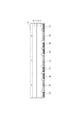
図1は、画素の第一電極の平面図である。画素1は、R画素、G画素、B画素の3つの副画素を有している。各副画素の第一電極4は第一画素電極2と第二画素電極3とを有している。第一画素電極2と隣接する副画素の第一画素電極2との間には、第二画素電極3が配置されている。例えば、G画素の第一画素電極2GとB画素の第一画素電極2Bとの間には、第二画素電極3G及び第二画素電極3Bが配置されている。各第一電極上には不図示の有機EL層が複数の画素に亘って共通層として設けられている。共通層とは、平面内において分離されることなく形成されている層である。
[First Embodiment]
[Electrode configuration of organic EL display device]
FIG. 1 is a plan view of the first electrode of the pixel.
表示装置は、第一画素電極及び第二画素電極に供給する電流の比率を制御する制御部を有してよい。 The display device may have a control unit that controls the ratio of the current supplied to the first pixel electrode and the second pixel electrode.
制御部は副画素間のリーク電流を低減するために、表示しようとする輝度が小さいほど第二画素電極3に対して第一画素電極2に流れる電流の比率が大きくなるよう制御してよい。反対に、表示しようとする輝度が大きいほど、第二画素電極3に対して第一画素電極2に流れる電流の比率は小さくなるよう制御してよい。さらには、HDR表示を行うために高輝度の発光が必要な場合は、上記の比率を考慮せずに第一及び第二画素電極に電流を供給してもよい。表示装置は、第一画素電極及び第二画素電極に供給する電流の比率を考慮しない、HDRモードを有してよい。特に有機EL素子を用いる場合は、コントラスト比が高いので、HDR表示を有利に行うことができる。 In order to reduce the leakage current between the sub-pixels, the control unit may control so that the smaller the brightness to be displayed, the larger the ratio of the current flowing through the first pixel electrode 2 to the second pixel electrode 3. On the contrary, the larger the brightness to be displayed, the smaller the ratio of the current flowing through the first pixel electrode 2 to the second pixel electrode 3 may be controlled. Furthermore, when high-luminance light emission is required for HDR display, current may be supplied to the first and second pixel electrodes without considering the above ratio. The display device may have an HDR mode that does not consider the ratio of the currents supplied to the first pixel electrode and the second pixel electrode. In particular, when an organic EL element is used, the HDR display can be advantageously performed because the contrast ratio is high.
図2は赤(R)、緑(G)、青(B)の3つの副画素から成る画素の断面図である。図1と同じ構成部材には同じ符号が付されている。各副画素の画素電極は第一画素電極2と第二画素電極3に分割されている。副画素電極と副画素電極の間には絶縁層である素子分離層5が配置されている。素子分離層はバンクとも呼ばれる。 FIG. 2 is a cross-sectional view of a pixel composed of three sub-pixels of red (R), green (G), and blue (B). The same components as those in FIG. 1 are designated by the same reference numerals. The pixel electrode of each sub-pixel is divided into a first pixel electrode 2 and a second pixel electrode 3. An element separation layer 5 which is an insulating layer is arranged between the sub-pixel electrode and the sub-pixel electrode. The element separation layer is also called a bank.
各画素電極及び素子分離層5の上には白色を発光する有機EL層6が平面的に分離されることなく共通層として設けられている。有機EL層6には例えば電荷注入層や発光層等を順に堆積させることで、機能に応じた有機層を形成する。有機EL層6の上には第二電極7が全副画素共通に設けられている。第二電極は、全画素に共通で設けられてもよい。共通で設けられるとは、平面的に分離されることなく配置されることを指す。 An organic EL layer 6 that emits white light is provided as a common layer on each pixel electrode and the element separation layer 5 without being separated in a plane. For example, a charge injection layer, a light emitting layer, and the like are sequentially deposited on the organic EL layer 6 to form an organic layer according to the function. A second electrode 7 is provided on the organic EL layer 6 in common with all sub-pixels. The second electrode may be provided in common to all pixels. Commonly provided means that they are arranged without being separated in a plane.
第二電極7の上には絶縁層8が積層され、絶縁層8の上にはカラーフィルタ9が形成されている。赤(R)、緑(G)、青(B)の3つの副画素に対応したカラーフィルタと白色に発光する有機EL素子と組み合わせることにより、白色光からR、G、Bの各色光を取り出すことができる。
An insulating
次に低輝度時に色再現性が向上する理由をG画素のみ低輝度を表示させる場合の例を用いて説明する。G画素に低輝度を表示させる場合、画素電極3Gに対して画素電極2Gに流れる電流比率が大きくなってよい。画素電極2Gは画素電極3Gよりも隣接する副画素の画素電極(2R、3R、2B、3B)との距離が十分に大きいため、隣接副画素へのリーク電流が発生しがたい画素である。そのため、隣接する副画素へのリーク電流を抑制することができる。隣接する副画素に流れるリーク電流が低減すると、隣接する副画素がリーク電流によって発光する量を抑制できるため、色再現性を向上させることができる。
Next, the reason why the color reproducibility is improved at low brightness will be described with an example of displaying low brightness only for G pixels. When displaying low brightness on the G pixel, the ratio of the current flowing through the
色再現性の低下は、特に低輝度時において顕著である。それは、微小な電流を画素電極に流して発光させる場合、隣接画素へリークする電流の割合が増加するからである。 The decrease in color reproducibility is particularly remarkable at low brightness. This is because when a minute current is passed through the pixel electrodes to emit light, the proportion of the current leaking to the adjacent pixels increases.
色再現性を向上させる効果は、表示装置が低輝度を表示しようとする場合に効果が高いので、上記の制御は、所定以下の輝度を表示しようとする場合に用いてもよい。 Since the effect of improving the color reproducibility is high when the display device tries to display low brightness, the above control may be used when trying to display brightness below a predetermined value.
具体的には、G画素が発光する際に、R画素又はB画素の発光を抑制することができるので、意図した緑色を発光することができる。R画素やB画素においても同様である。その結果、RGBの発光色を色度座標上に表し、それぞれを線分で繋ぐことで描いた三角形の面積を大きくすることができる。 Specifically, when the G pixel emits light, the emission of the R pixel or the B pixel can be suppressed, so that the intended green can be emitted. The same applies to the R pixel and the B pixel. As a result, the area of the drawn triangle can be increased by expressing the emission color of RGB on the chromaticity coordinates and connecting each with a line segment.
一方、G画素に高輝度を表示させようとする場合は、画素電極3Gに対して画素電極2Gに流れる電流比率が小さくなってよい。画素電極3Gは隣接する副画素の画素電極、特に第一電極4R及び第一電極4Bとの距離が、画素電極2Gの場合よりも小さいため、リーク電流は流れやすい。しかし、低輝度を表示させようとする場合よりも大きな電流が画素電極3Gに流れるため、画素電極3Gに流れる電流に対するリーク電流の比率は低輝度を表示する場合に比べて小さい。そのため、低輝度を表示させる場合よりもリーク電流の影響が軽微であり、色再現性への影響も小さい。
On the other hand, when the G pixel is intended to display high brightness, the ratio of the current flowing through the
図1では、第一電極がストライプ状に配置される例を示しているが、これに限らない。例えば、図3に示す平面図のようにデルタ配列であってよい。デルタ配列は、各副画素を頂点として、三角形(デルタ)の形状に配置される配列である。 FIG. 1 shows an example in which the first electrodes are arranged in a stripe shape, but the present invention is not limited to this. For example, it may be a delta array as shown in the plan view shown in FIG. The delta array is an array arranged in a triangular shape with each sub-pixel as a vertex.
[有機EL表示装置の回路構成]
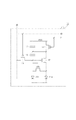
図4は、本発明の有機EL表示装置に用いられる画素回路の一例である。図4において、副画素10は、有機EL素子11と、有機EL素子11を駆動する駆動回路とによって構成されている。有機EL素子11は、11aと11bとに分けて記載されている。有機EL素子11は全副画素10に対して共通に設けられた第二電極18が接続されている。第二電極はカソード電極であってよい。有機EL素子11の第一電極である、アノード電極は、副画素毎に2つに分割されているため有機EL素子11a、有機EL素子11bと表すことができる。有機EL素子11aは、第一画素電極に電流を供給する回路であり、有機EL素子11bは第二画素電極に電流を供給する回路である。
[Circuit configuration of organic EL display device]
FIG. 4 is an example of a pixel circuit used in the organic EL display device of the present invention. In FIG. 4, the sub-pixel 10 is composed of an organic EL element 11 and a drive circuit for driving the organic EL element 11. The organic EL element 11 is described separately as 11a and 11b. The organic EL element 11 is connected to a second electrode 18 that is commonly provided for all the sub-pixels 10. The second electrode may be a cathode electrode. Since the anode electrode, which is the first electrode of the organic EL element 11, is divided into two for each sub-pixel, it can be represented as an
有機EL素子11を駆動する駆動回路は、駆動トランジスタ12、選択トランジスタ13、スイッチングトランジスタ14、電流制御用トランジスタ15及び第一容量素子16、第二容量素子17を有する。駆動トランジスタ12、選択トランジスタ13、スイッチングトランジスタ14、電流制御用トランジスタ15は、Pチャネル型のトランジスタであってよい。
The drive circuit for driving the organic EL element 11 includes a
駆動トランジスタ12は、有機EL素子11a及び有機EL素子11bに接続されており、有機EL素子11a及び有機EL素子11bに駆動電流を供給する。具体的には、駆動トランジスタ12のドレイン電極が有機EL素子11a及び有機EL素子11bのアノード電極に接続されている。
The
選択トランジスタ13は、ゲート電極が走査線19に接続され、ソース電極が信号線20に接続され、ドレイン電極が駆動トランジスタ12のゲート電極に接続されている。選択トランジスタ13のゲート電極には、不図示の垂直駆動回路から走査線19を通して書き込まれた信号が印加される。
In the
スイッチングトランジスタ14は、ゲート電極が走査線21に接続され、ソース電極が第一電源電位VDDに接続され、ドレイン電極が駆動トランジスタ12のソース電極に接続されている。スイッチングトランジスタ14のゲート電極には、垂直駆動回路から走査線21を通して発光を制御するための信号が印加される。
In the switching
第一容量素子16は、駆動トランジスタ12のゲート電極とソース電極との間に接続されている。第二容量素子17は、駆動トランジスタ12のソース電極と第一電源電位VDDとの間に接続されている。
The
走査線19、21が接続されている垂直駆動回路は、行単位で順次信号を供給することによって、信号電圧及び基準電圧を各画素の保持容量素子に保持させ、信号電圧に応じた輝度で画素が発光するように制御する。
The vertical drive circuit to which the
上記構成の副画素10において、選択トランジスタ13は、垂直駆動回路から走査線19を通してゲート電極に印加される書き込み信号に応答して導通状態になる。この動作によって輝度情報に応じた信号電圧又は基準電圧をサンプリングして副画素10内に書き込む。基準電圧を印加することによって各画素の駆動トランジスタ12の閾値電圧ばらつきを補正し、閾値電圧ばらつきによる各画素の輝度ばらつきを低減することができる。書き込まれた信号電圧又は基準電圧は駆動トランジスタ12のゲート電極に印加されるとともに第一容量素子16に保持される。
In the sub-pixel 10 having the above configuration, the
スイッチングトランジスタ14は、垂直駆動回路から走査線21を通して発光を制御するための信号がゲート電極に印加されることで導通状態になる。すなわち、有機EL素子11の発光、非発光を制御する機能を有している。
The switching
駆動トランジスタ12は飽和領域で動作するように設計されている。駆動トランジスタ12は電源電位VDDからスイッチングトランジスタ14を介して電流の供給を受けて有機EL素子11a及び有機EL素子11bを電流駆動にて発光させる。この際、第一容量素子16に保持された電圧に応じて有機EL素子11に流れる電流量が決まるため、有機EL素子の発光量を制御することができる。
The
電流制御用トランジスタ15は有機EL素子11bに流れる電流を制御するためのトランジスタである。ゲート電極が駆動トランジスタ12のゲート電極と接続されているため、第一容量素子16に保持された電圧に応じて導通状態を制御することができる。すなわち、駆動トランジスタ12を通して供給される電流に対して有機EL素子11aと有機EL素子11bに流す電流の比率を制御することができる。
The current control transistor 15 is a transistor for controlling the current flowing through the
電流制御用トランジスタ15は、第二画素電極に接続されたトランジスタであり、入力信号の大きさに応じて、第二画素電極に供給する電流を大きくする構成であってよい。 The current control transistor 15 is a transistor connected to the second pixel electrode, and may be configured to increase the current supplied to the second pixel electrode according to the magnitude of the input signal.
本実施形態の場合、入力される信号電圧が表示される輝度として小さいほど有機EL素子11bよりも有機EL素子11aに流れる電流の比率が大きくなってよい。また、入力される信号電圧が表示される輝度として大きいほど有機EL素子11bに流れる電流は大きくなってよい。輝度によって有機EL素子11aと11bに流れる電流の比率をどの程度にするかは、電流制御用トランジスタ18の閾値を調整するなどして制御することが可能である。
In the case of the present embodiment, the smaller the displayed brightness of the input signal voltage, the larger the ratio of the current flowing through the
本実施形態においては、電流制御用トランジスタ15を用いた回路で有機EL素子11aと有機EL素子11bに流れる電流を制御している。しかし、有機EL素子11aと有機EL素子11bに流れる電流の比率を制御できるのであれば、この回路構成に限られるものではない。
In the present embodiment, the current flowing through the
図4では、MOSトランジスタとしてPMOSを用いているが、NMOSを用いてもよい。また、駆動回路として3つのトランジスタと2つの容量素子からなる回路構成のものに限られるものではない。また、MOSトランジスタとしては、シリコンウェーハ上に形成したトランジスタを用いてもよいし、ガラス基板上に形成した薄膜トランジスタを用いてもよい。 In FIG. 4, a MOSFET is used as the MOS transistor, but an NMOS may be used. Further, the drive circuit is not limited to a circuit configuration including three transistors and two capacitive elements. Further, as the MOS transistor, a transistor formed on a silicon wafer may be used, or a thin film transistor formed on a glass substrate may be used.
図5は、本発明の有機EL表示装置の一例を示す全体概略図である。有機EL表示装置22は、表示領域23、水平駆動回路24、垂直駆動回路25、接続端子部26を備えている。表示領域23には、複数の画素がマトリックス状に配置されている。各画素は、赤(R)、緑(G)、青(B)の副画素を有している。各副画素には、図4の画素回路が配置されている。
FIG. 5 is an overall schematic view showing an example of the organic EL display device of the present invention. The organic EL display device 22 includes a
水平駆動回路24はデータ信号を出力する回路であり、データ線20と接続されている。垂直駆動回路25は選択信号を出力する回路である。接続端子部26は水平駆動回路24、垂直駆動回路25にクロック信号、画像データ信号等を入力する端子であり、配線(不図示)によって水平駆動回路24、垂直駆動回路25と接続されている。
The
以上述べたように、本発明では、低輝度を表示する場合に主に電流を流す第一画素電極2を隣接する副画素の第一電極から遠い位置に配置することが好ましい。 As described above, in the present invention, it is preferable to arrange the first pixel electrode 2 that mainly conducts current when displaying low brightness at a position far from the first electrode of the adjacent sub-pixel.
[第二の実施形態]
図6は、本実施形態に係る画素の平面図である。本実施形態は、特定の副画素の第一電極のみが、第一画素電極及び第二画素電極を有し、その他の副画素の第一電極は分割されていないことを除いて、第一の実施形態と同じである。第一の実施形態の構造及び説明は本実施形態においても同様に適用することが可能である。
[Second Embodiment]
FIG. 6 is a plan view of the pixels according to the present embodiment. In this embodiment, the first electrode of a specific sub-pixel has a first pixel electrode and a second pixel electrode, and the first electrode of the other sub-pixel is not divided. It is the same as the embodiment. The structure and description of the first embodiment can be similarly applied to this embodiment.
図6ではG画素のみ画素電極が第一画素電極2G、第二画素電極3Gに分割されている。R画素及びB画素は画素電極4が分割されていない。G画素の画素回路は図4のように有機EL素子11aと有機EL素子11bに流す電流比率を制御するための電流制御用トランジスタ18が設けられている。一方、R画素及びB画素は画素電極が分割されていないため、図11に示すように1つの有機EL素子11のみ設けられていて電流制御用トランジスタは設けられていない。
In FIG. 6, the pixel electrode of only the G pixel is divided into the
本実施形態では、R画素及びB画素に比べてG画素を多く発光させる場合の低輝度時の色再現性を向上させたい場合に有効である。R画素及びB画素の画素電極は分割されていないため、分割させた場合に比べて発光面積を大きく確保することが可能になり、発光効率を向上させることができる。 In this embodiment, it is effective when it is desired to improve the color reproducibility at low brightness when a large number of G pixels are emitted as compared with R pixels and B pixels. Since the pixel electrodes of the R pixel and the B pixel are not divided, it is possible to secure a large light emitting area as compared with the case of being divided, and it is possible to improve the luminous efficiency.
[第三の実施形態]
図7は、本実施形態に係る画素の平面図である。本実施形態は、同じ色を発光する副画素の第一画素電極同士の間には、第二画素電極を設けないことを除いて、第一の実施形態と同じである。実施例1の構造及び説明は本実施例においても同様に適用することが可能である。
[Third Embodiment]
FIG. 7 is a plan view of the pixels according to the present embodiment. This embodiment is the same as the first embodiment except that a second pixel electrode is not provided between the first pixel electrodes of the sub-pixels that emit the same color. The structure and description of Example 1 can be similarly applied to this Example.
本実施形態では、異なる色を表示する副画素間においては、第一画素電極と隣接する副画素における第一電極の間に第二画素電極が配置されているが、同じ色を発光する副画素間においては第二画素電極を設けない。すなわち、第一画素電極の平面における形状が、多角形であり、前記第一画素電極の少なくともいずれか一辺は、前記第二画素電極に接していない構成としてよい。 In the present embodiment, between the sub-pixels displaying different colors, the second pixel electrode is arranged between the first pixel electrode and the first electrode of the adjacent sub-pixel, but the sub-pixels emitting the same color. No second pixel electrode is provided between them. That is, the shape of the first pixel electrode on the plane may be polygonal, and at least one side of the first pixel electrode may not be in contact with the second pixel electrode.
例えば、G画素の第一画素電極と隣接するG画素の第一画素電極の間には第二画素電極は設けられていないため、G画素の第一画素電極間の距離は異色の第一画素電極間の距離よりも小さい。そのため、隣接する同色の画素電極間のリーク電流は、隣接する異色の画素電極間のリーク電流よりも大きくなるが、同じ色の画素同士のリーク電流なので色再現性に与える影響は小さい。 For example, since the second pixel electrode is not provided between the first pixel electrode of the G pixel and the first pixel electrode of the adjacent G pixel, the distance between the first pixel electrodes of the G pixel is a different color of the first pixel. It is smaller than the distance between the electrodes. Therefore, the leak current between adjacent pixel electrodes of the same color is larger than the leak current between adjacent pixel electrodes of different colors, but since it is a leak current between pixels of the same color, the effect on color reproducibility is small.
また、第一の実施形態に比べて、第一画素電極の発光面積を大きく確保することが可能になり、発光効率を向上させることができる。 Further, as compared with the first embodiment, it is possible to secure a large light emitting area of the first pixel electrode, and it is possible to improve the light emitting efficiency.
[その他の形態]
本発明に係る表示装置は、基板を有してよい。基板は、高い強度を有する基板であっても、フレキシブル基板であってもよい。具体的には、ガラス基板、シリコン基板等の強度が高い基板であってよい。また、ポリアクリル基板、ポリイミド基板等のフレキシブル基板であってよい。
[Other forms]
The display device according to the present invention may have a substrate. The substrate may be a substrate having high strength or a flexible substrate. Specifically, it may be a substrate having high strength such as a glass substrate or a silicon substrate. Further, it may be a flexible substrate such as a polyacrylic substrate or a polyimide substrate.
本発明に係る表示装置は、基板から、第一電極、機能層、第二電極、の順に配置されてよい。また、第一電極側から発光を取り出すボトムエミッションタイプであっても、第二電極側から発光を取り出すトップエミッションタイプであってもよい。 The display device according to the present invention may be arranged in the order of the first electrode, the functional layer, and the second electrode from the substrate. Further, it may be a bottom emission type that extracts light emission from the first electrode side or a top emission type that extracts light emission from the second electrode side.
本発明に係る表示装置は、第一電極がアノード電極であってよい。また、第一電極がカソード電極であってもよい。また、第一電極が反射電極であってよい。また第一電極が透過電極であってもよい。第一電極が基板側に配置され、反射性を有するアノード電極であってよい。第一電極が基板側に配置され、かつカソード電極である場合は、耐水性が比較的低い電子注入層や電子輸送層が、外気と離れて配置されるので、表示装置として耐水性が高い。この場合、カソード電極は、反射性であっても、透過性であってもよい。 In the display device according to the present invention, the first electrode may be an anode electrode. Further, the first electrode may be a cathode electrode. Further, the first electrode may be a reflective electrode. Further, the first electrode may be a transmission electrode. The first electrode may be an anode electrode which is arranged on the substrate side and has reflectivity. When the first electrode is arranged on the substrate side and is a cathode electrode, the electron injection layer and the electron transport layer having relatively low water resistance are arranged away from the outside air, so that the water resistance of the display device is high. In this case, the cathode electrode may be reflective or transmissive.
アノード電極の構成材料としては、例えば、金、白金、銀、銅、アルミニウム、チタン、ニッケル、パラジウム、コバルト、セレン、バナジウム、タングステン等の金属単体あるいはこれらを組み合わせた合金、酸化錫、酸化亜鉛、酸化インジウム、酸化錫インジウム(ITO)、酸化亜鉛インジウム等の金属酸化物が使用できる。またポリアニリン、ポリピロール、ポリチオフェン等の導電性ポリマーも使用できる。 Examples of the constituent materials of the anode electrode include simple metals such as gold, platinum, silver, copper, aluminum, titanium, nickel, palladium, cobalt, selenium, vanadium, and tungsten, or alloys obtained by combining these, tin oxide, zinc oxide, and the like. Metal oxides such as indium oxide, indium tin oxide (ITO), and indium zinc oxide can be used. Also, conductive polymers such as polyaniline, polypyrrole and polythiophene can be used.
これらの電極物質は一種類を単独で使用してもよいし、二種類以上を併用して使用してもよい。また、アノード電極は一層で構成されていてもよく、複数の層で構成されていてもよい。 One type of these electrode substances may be used alone, or two or more types may be used in combination. Further, the anode electrode may be composed of one layer or may be composed of a plurality of layers.
一方、陰極の構成材料としては、例えばリチウム等のアルカリ金属、カルシウム等のアルカリ土類金属、アルミニウム、チタニウム、マンガン、銀、鉛、クロム等の金属単体が挙げられる。あるいはこれら金属単体を組み合わせた合金も使用することができる。例えばマグネシウム−銀、アルミニウム−リチウム、アルミニウム−マグネシウム等が使用できる。酸化錫インジウム(ITO)等の金属酸化物の利用も可能である。これらの電極物質は一種類を単独で使用してもよいし、二種類以上を併用して使用してもよい。また陰極は一層構成でもよく、多層構成でもよい。 On the other hand, examples of the constituent material of the cathode include alkali metals such as lithium, alkaline earth metals such as calcium, and simple metals such as aluminum, titanium, manganese, silver, lead, and chromium. Alternatively, an alloy in which these metal simple substances are combined can also be used. For example, magnesium-silver, aluminum-lithium, aluminum-magnesium and the like can be used. It is also possible to use a metal oxide such as indium tin oxide (ITO). One type of these electrode substances may be used alone, or two or more types may be used in combination. Further, the cathode may have a single-layer structure or a multi-layer structure.
本発明に係る有機EL素子を構成する有機EL層は、一層であっても、多層で構成されてもよい。多層で構成される場合は、正孔注入層、正孔輸送層、電子阻止層、発光層、正孔阻止層、電子輸送層、電子注入層等が挙げられる。 The organic EL layer constituting the organic EL element according to the present invention may be composed of one layer or multiple layers. When it is composed of multiple layers, examples thereof include a hole injection layer, a hole transport layer, an electron blocking layer, a light emitting layer, a hole blocking layer, an electron transport layer, and an electron injection layer.
本発明に係る有機EL素子を構成する有機EL層は、真空蒸着法、イオン化蒸着法、スパッタリング、プラズマ等のドライプロセスを用いて製造することができる。またドライプロセスに代えて、適当な溶媒に溶解させて公知の塗布法(例えば、スピンコーティング、ディッピング、キャスト法、LB法、インクジェット法等)により層を形成するウェットプロセスを用いることもできる。 The organic EL layer constituting the organic EL element according to the present invention can be produced by using a dry process such as a vacuum vapor deposition method, an ionization vapor deposition method, sputtering, or plasma. Further, instead of the dry process, a wet process in which a layer is formed by dissolving in an appropriate solvent and forming a layer by a known coating method (for example, spin coating, dipping, casting method, LB method, inkjet method, etc.) can also be used.
ここで真空蒸着法や溶液塗布法等によって層を形成すると、結晶化等が起こりにくく経時安定性に優れる。また塗布法で成膜する場合は、適当なバインダー樹脂と組み合わせて膜を形成することもできる。 Here, when a layer is formed by a vacuum deposition method, a solution coating method, or the like, crystallization or the like is unlikely to occur and the stability over time is excellent. Further, when the film is formed by the coating method, the film can be formed by combining with an appropriate binder resin.
上記バインダー樹脂としては、ポリビニルカルバゾール樹脂、ポリカーボネート樹脂、ポリエステル樹脂、ABS樹脂、アクリル樹脂、ポリイミド樹脂、フェノール樹脂、エポキシ樹脂、シリコン樹脂、尿素樹脂等が挙げられるが、これらに限定されるものではない。 Examples of the binder resin include, but are not limited to, polyvinylcarbazole resin, polycarbonate resin, polyester resin, ABS resin, acrylic resin, polyimide resin, phenol resin, epoxy resin, silicon resin, urea resin and the like. ..
また、これらバインダー樹脂は、ホモポリマー又は共重合体として一種類を単独で使用してもよいし、二種類以上を混合して使用してもよい。さらに必要に応じて、公知の可塑剤、酸化防止剤、紫外線吸収剤等の添加剤を併用してもよい。 Further, these binder resins may be used alone as a homopolymer or a copolymer, or may be used as a mixture of two or more kinds. Further, if necessary, known additives such as a plasticizer, an antioxidant, and an ultraviolet absorber may be used in combination.
表示装置はPC用のディスプレイ等の表示装置として用いることができる。また、エリアCCD、リニアCCD、メモリーカード等からの画像情報を入力する入力部を有し、入力された情報を処理する情報処理部を有し、入力された画像を表示部に表示する画像表示装置でもあってよい。 The display device can be used as a display device such as a display for a PC. Further, it has an input unit for inputting image information from an area CCD, a linear CCD, a memory card, etc., has an information processing unit for processing the input information, and displays an image displayed on the display unit. It may also be a device.
また、撮像装置やインクジェットプリンタが有する表示部として用いられてもよい。表示部は、撮像素子により撮像された画像を表示する表示部であってよい。その場合、表示装置は、外部から入力された画像情報を表示する画像出力機能と操作パネルとして画像への加工情報を入力する入力機能との両方を有していてもよい。入力機能を有する場合は、タッチパネル機能を有していてもよい。タッチパネル機能の方式は、静電容量方式でも、抵抗膜方式でも、赤外線方式であってもよい。また、入力機能は音声入力であってもよい。 Further, it may be used as a display unit included in an image pickup apparatus or an inkjet printer. The display unit may be a display unit that displays an image captured by the image sensor. In that case, the display device may have both an image output function for displaying image information input from the outside and an input function for inputting processing information to the image as an operation panel. When it has an input function, it may have a touch panel function. The touch panel function method may be a capacitance method, a resistive film method, or an infrared method. Further, the input function may be voice input.
また、撮像装置の表示装置に用いられる場合は、撮像装置の筐体に設けられる表示装置であっても、ビューファインダーとして用いられてもよい。 When it is used as a display device of an image pickup device, it may be a display device provided in a housing of the image pickup device or may be used as a viewfinder.
撮像装置は、複数のレンズを有する光学系と、前記レンズを通過した光を受光する撮像素子とを有してよい。 The image pickup device may include an optical system having a plurality of lenses and an image pickup element that receives light that has passed through the lenses.
また撮像装置は、筐体とこの筐体に格納された撮像素子を有し、この筐体は、複数のレンズを有する光学系が接続可能であってよい。 Further, the image pickup apparatus has a housing and an image pickup element housed in the housing, and an optical system having a plurality of lenses may be connected to the housing.
以上の通り、本発明によれば、副画素から、当該副画素と異なる発光色である隣接副画素への影響を抑制することで、色再現性に優れた表示装置を提供できる。 As described above, according to the present invention, it is possible to provide a display device having excellent color reproducibility by suppressing the influence of the sub-pixel on the adjacent sub-pixel, which is a emission color different from that of the sub-pixel.
1 画素
2 第一画素電極
3 第二画素電極
4 第一電極
5 素子分離層
6 有機EL層
7 第二電極
8 絶縁層
9 カラーフィルタ
1 pixel 2 1st pixel electrode 3
Claims (19)
前記第一の副画素及び前記第二の副画素は、第一電極と、第二電極と、前記第一電極と前記第二電極との間に配置されている機能層とを有し、
前記第一の副画素の前記第一電極は、第一画素電極と前記第一画素電極と隣り合う第二画素電極とを有し、
前記第一の副画素の第一画素電極に電流を供給する第一のトランジスタと、前記第一の副画素の第二画素電極に電流を供給する第二のトランジスタとを有し、
いずれの前記第一の副画素及び前記第二の副画素においても、前記第一の副画素の前記第一画素電極と前記第二の副画素の前記第一電極との間に、前記第一の副画素の前記第二画素電極が配置され、
前記第一のトランジスタは、前記第二のトランジスタを介して前記第二の画素電極に電流を供給することを特徴とする表示装置。 It has a first sub-pixel and a second sub-pixel having an emission color different from that of the first sub-pixel, and the first sub-pixel and the second sub-pixel are arranged adjacent to each other. It is a display device equipped with pixels
The first sub-pixel and the second sub-pixel have a first electrode, a second electrode, and a functional layer arranged between the first electrode and the second electrode.
The first electrode of the first sub-pixel has a first pixel electrode and a second pixel electrode adjacent to the first pixel electrode.
It has a first transistor that supplies a current to the first pixel electrode of the first sub-pixel and a second transistor that supplies a current to the second pixel electrode of the first sub-pixel.
In any of the first sub-pixels and the second sub-pixel, the first is placed between the first pixel electrode of the first sub-pixel and the first electrode of the second sub-pixel. the second pixel electrode of the sub-pixels are arranged in,
The first transistor is a display device characterized by supplying a current to the second pixel electrode via the second transistor.
前記第一の副画素及び前記第二の副画素は、第一電極と、第二電極と、前記第一電極と前記第二電極との間に配置されている機能層とを有し、
前記第一の副画素の前記第一電極は、第一画素電極と前記第一画素電極と隣り合う第二画素電極とを有し、前記第一の副画素のみが、前記第一画素電極及び前記第二画素電極を有し、
前記第一の副画素の前記第一画素電極と前記第二の副画素の前記第一電極との間に、前記第一の副画素の前記第二画素電極が配置されていることを特徴とする表示装置。 It has a first sub-pixel and a second sub-pixel having an emission color different from that of the first sub-pixel, and the first sub-pixel and the second sub-pixel are arranged adjacent to each other. It is a display device equipped with pixels
The first sub-pixel and the second sub-pixel have a first electrode, a second electrode, and a functional layer arranged between the first electrode and the second electrode.
The first electrode of the first sub-pixel has a first pixel electrode and a second pixel electrode adjacent to the first pixel electrode, and only the first sub-pixel has the first pixel electrode and the first sub-pixel. It has the second pixel electrode and
The feature is that the second pixel electrode of the first sub-pixel is arranged between the first pixel electrode of the first sub-pixel and the first electrode of the second sub-pixel. Display device.
前記表示装置は、請求項1乃至18のいずれか一項に記載の表示装置であることを特徴とする撮像装置。 An image pickup device having an optical system having a plurality of lenses, an image pickup device that receives light that has passed through the optical system, and a display device that displays the captured image.
The image pickup device according to any one of claims 1 to 18 , wherein the display device is the display device.
Priority Applications (2)
| Application Number | Priority Date | Filing Date | Title |
|---|---|---|---|
| JP2017183510A JP6932596B2 (en) | 2017-09-25 | 2017-09-25 | Organic EL display device |
| US16/129,430 US10769993B2 (en) | 2017-09-25 | 2018-09-12 | Organic electroluminescence display apparatus |
Applications Claiming Priority (1)
| Application Number | Priority Date | Filing Date | Title |
|---|---|---|---|
| JP2017183510A JP6932596B2 (en) | 2017-09-25 | 2017-09-25 | Organic EL display device |
Publications (3)
| Publication Number | Publication Date |
|---|---|
| JP2019061777A JP2019061777A (en) | 2019-04-18 |
| JP2019061777A5 JP2019061777A5 (en) | 2020-09-10 |
| JP6932596B2 true JP6932596B2 (en) | 2021-09-08 |
Family
ID=65807874
Family Applications (1)
| Application Number | Title | Priority Date | Filing Date |
|---|---|---|---|
| JP2017183510A Active JP6932596B2 (en) | 2017-09-25 | 2017-09-25 | Organic EL display device |
Country Status (2)
| Country | Link |
|---|---|
| US (1) | US10769993B2 (en) |
| JP (1) | JP6932596B2 (en) |
Families Citing this family (5)
| Publication number | Priority date | Publication date | Assignee | Title |
|---|---|---|---|---|
| KR102503168B1 (en) * | 2018-02-08 | 2023-02-27 | 삼성디스플레이 주식회사 | Display device and fabricating method thereof |
| DE102019112456B4 (en) | 2019-05-13 | 2023-05-25 | OSRAM Opto Semiconductors Gesellschaft mit beschränkter Haftung | INDICATOR AND METHOD OF OPERATION FOR AN INDICATOR |
| CN210516181U (en) * | 2019-09-29 | 2020-05-12 | 昆山国显光电有限公司 | Transparent display substrate and display device |
| KR20220006164A (en) * | 2020-07-07 | 2022-01-17 | 삼성디스플레이 주식회사 | Display device |
| CN111986621B (en) | 2020-08-06 | 2022-12-23 | 武汉华星光电半导体显示技术有限公司 | OLED display panel |
Family Cites Families (15)
| Publication number | Priority date | Publication date | Assignee | Title |
|---|---|---|---|---|
| JP4822590B2 (en) * | 2001-02-08 | 2011-11-24 | 三洋電機株式会社 | Organic EL circuit |
| JP4196622B2 (en) * | 2002-09-06 | 2008-12-17 | セイコーエプソン株式会社 | Color balance adjusting device and electronic device |
| JP4459521B2 (en) * | 2002-10-17 | 2010-04-28 | 大日本印刷株式会社 | Electroluminescence display device |
| JP2010021138A (en) * | 2008-06-09 | 2010-01-28 | Panasonic Corp | Organic electroluminescent device and its manufacturing method |
| US8237642B2 (en) * | 2008-07-14 | 2012-08-07 | Global Oled Technology Llc | Method for improving display lifetime |
| WO2010100789A1 (en) * | 2009-03-05 | 2010-09-10 | シャープ株式会社 | Active matrix substrate, method for producing active matrix substrate, liquid crystal panel, method for producing liquid crystal panel, liquid crystal display device, liquid crystal display unit, and television receiver |
| JP2010230797A (en) * | 2009-03-26 | 2010-10-14 | Seiko Epson Corp | Display device, and electronic apparatus |
| KR101328979B1 (en) * | 2011-06-30 | 2013-11-13 | 삼성디스플레이 주식회사 | Organic light emitting display device |
| JP5961060B2 (en) * | 2012-07-18 | 2016-08-02 | 株式会社ジャパンディスプレイ | Liquid crystal display |
| JP2014086236A (en) * | 2012-10-23 | 2014-05-12 | Seiko Epson Corp | Light-emitting device, and electronic apparatus |
| JP6257259B2 (en) * | 2013-10-18 | 2018-01-10 | 株式会社ジャパンディスプレイ | Display device |
| JP6311868B2 (en) * | 2013-11-07 | 2018-04-18 | 株式会社Joled | Image processing circuit, image processing method, and display device |
| JP6285158B2 (en) | 2013-11-26 | 2018-02-28 | 株式会社ジャパンディスプレイ | Organic EL display device |
| JP2017083517A (en) * | 2015-10-23 | 2017-05-18 | 株式会社ジャパンディスプレイ | Display device and manufacturing method of the same |
| US10127859B2 (en) * | 2016-12-29 | 2018-11-13 | Lg Display Co., Ltd. | Electroluminescent display |
-
2017
- 2017-09-25 JP JP2017183510A patent/JP6932596B2/en active Active
-
2018
- 2018-09-12 US US16/129,430 patent/US10769993B2/en active Active
Also Published As
| Publication number | Publication date |
|---|---|
| US20190096324A1 (en) | 2019-03-28 |
| JP2019061777A (en) | 2019-04-18 |
| US10769993B2 (en) | 2020-09-08 |
Similar Documents
| Publication | Publication Date | Title |
|---|---|---|
| JP6932596B2 (en) | Organic EL display device | |
| US10541277B2 (en) | Organic light emitting display device | |
| US11005064B2 (en) | Transparent display substrate and driving method thereof and transparent display device | |
| CN109509772B (en) | Organic light emitting diode display | |
| US11075253B2 (en) | Organic light-emitting display device | |
| KR102449131B1 (en) | Organic light emitting display device | |
| US9219103B2 (en) | Organic light emitting diode display | |
| US10686022B2 (en) | Organic light emitting diode display | |
| KR101736929B1 (en) | White organic light emitting diode display device | |
| US10608199B2 (en) | Display apparatus | |
| KR102423799B1 (en) | Organic light emitting display device | |
| US11211440B2 (en) | Display device, method of manufacturing display device, and electronic apparatus with contact electrode | |
| US9601720B2 (en) | Organic light emitting diode display | |
| US10566407B2 (en) | Organic light emitting diode display having barrier layer on auxiliary electrode | |
| KR102433353B1 (en) | Organic light emitting display device | |
| CN111326673B (en) | Display device | |
| JP2009169070A (en) | Color image display device, shadow mask and method of manufacturing color image display device using shadow mask | |
| US20240065028A1 (en) | Display device and pixel array substrate thereof | |
| KR102579963B1 (en) | Display devices and electronic devices | |
| WO2021176894A1 (en) | Display device, method for manufacturing display device, and electronic apparatus | |
| US11869421B2 (en) | Display device | |
| KR20190062853A (en) | Organic light emitting display device | |
| JP2007072187A (en) | Organic el display device |
Legal Events
| Date | Code | Title | Description |
|---|---|---|---|
| A521 | Request for written amendment filed |
Free format text: JAPANESE INTERMEDIATE CODE: A523 Effective date: 20200720 |
|
| A621 | Written request for application examination |
Free format text: JAPANESE INTERMEDIATE CODE: A621 Effective date: 20200720 |
|
| A977 | Report on retrieval |
Free format text: JAPANESE INTERMEDIATE CODE: A971007 Effective date: 20210317 |
|
| A131 | Notification of reasons for refusal |
Free format text: JAPANESE INTERMEDIATE CODE: A131 Effective date: 20210511 |
|
| A521 | Request for written amendment filed |
Free format text: JAPANESE INTERMEDIATE CODE: A523 Effective date: 20210629 |
|
| TRDD | Decision of grant or rejection written | ||
| A01 | Written decision to grant a patent or to grant a registration (utility model) |
Free format text: JAPANESE INTERMEDIATE CODE: A01 Effective date: 20210720 |
|
| A61 | First payment of annual fees (during grant procedure) |
Free format text: JAPANESE INTERMEDIATE CODE: A61 Effective date: 20210818 |
|
| R151 | Written notification of patent or utility model registration |
Ref document number: 6932596 Country of ref document: JP Free format text: JAPANESE INTERMEDIATE CODE: R151 |