WO2016140282A1 - Display device equipped with touch sensor - Google Patents
Display device equipped with touch sensor Download PDFInfo
- Publication number
- WO2016140282A1 WO2016140282A1 PCT/JP2016/056487 JP2016056487W WO2016140282A1 WO 2016140282 A1 WO2016140282 A1 WO 2016140282A1 JP 2016056487 W JP2016056487 W JP 2016056487W WO 2016140282 A1 WO2016140282 A1 WO 2016140282A1
- Authority
- WO
- WIPO (PCT)
- Prior art keywords
- electrode
- liquid crystal
- touch sensor
- display device
- substrate
- Prior art date
Links
Images


Classifications
-
- G—PHYSICS
- G02—OPTICS
- G02F—OPTICAL DEVICES OR ARRANGEMENTS FOR THE CONTROL OF LIGHT BY MODIFICATION OF THE OPTICAL PROPERTIES OF THE MEDIA OF THE ELEMENTS INVOLVED THEREIN; NON-LINEAR OPTICS; FREQUENCY-CHANGING OF LIGHT; OPTICAL LOGIC ELEMENTS; OPTICAL ANALOGUE/DIGITAL CONVERTERS
- G02F1/00—Devices or arrangements for the control of the intensity, colour, phase, polarisation or direction of light arriving from an independent light source, e.g. switching, gating or modulating; Non-linear optics
- G02F1/01—Devices or arrangements for the control of the intensity, colour, phase, polarisation or direction of light arriving from an independent light source, e.g. switching, gating or modulating; Non-linear optics for the control of the intensity, phase, polarisation or colour
- G02F1/13—Devices or arrangements for the control of the intensity, colour, phase, polarisation or direction of light arriving from an independent light source, e.g. switching, gating or modulating; Non-linear optics for the control of the intensity, phase, polarisation or colour based on liquid crystals, e.g. single liquid crystal display cells
-
- G—PHYSICS
- G06—COMPUTING; CALCULATING OR COUNTING
- G06F—ELECTRIC DIGITAL DATA PROCESSING
- G06F3/00—Input arrangements for transferring data to be processed into a form capable of being handled by the computer; Output arrangements for transferring data from processing unit to output unit, e.g. interface arrangements
- G06F3/01—Input arrangements or combined input and output arrangements for interaction between user and computer
- G06F3/03—Arrangements for converting the position or the displacement of a member into a coded form
- G06F3/041—Digitisers, e.g. for touch screens or touch pads, characterised by the transducing means
- G06F3/044—Digitisers, e.g. for touch screens or touch pads, characterised by the transducing means by capacitive means
- G06F3/0443—Digitisers, e.g. for touch screens or touch pads, characterised by the transducing means by capacitive means using a single layer of sensing electrodes
-
- G—PHYSICS
- G02—OPTICS
- G02F—OPTICAL DEVICES OR ARRANGEMENTS FOR THE CONTROL OF LIGHT BY MODIFICATION OF THE OPTICAL PROPERTIES OF THE MEDIA OF THE ELEMENTS INVOLVED THEREIN; NON-LINEAR OPTICS; FREQUENCY-CHANGING OF LIGHT; OPTICAL LOGIC ELEMENTS; OPTICAL ANALOGUE/DIGITAL CONVERTERS
- G02F1/00—Devices or arrangements for the control of the intensity, colour, phase, polarisation or direction of light arriving from an independent light source, e.g. switching, gating or modulating; Non-linear optics
- G02F1/01—Devices or arrangements for the control of the intensity, colour, phase, polarisation or direction of light arriving from an independent light source, e.g. switching, gating or modulating; Non-linear optics for the control of the intensity, phase, polarisation or colour
- G02F1/13—Devices or arrangements for the control of the intensity, colour, phase, polarisation or direction of light arriving from an independent light source, e.g. switching, gating or modulating; Non-linear optics for the control of the intensity, phase, polarisation or colour based on liquid crystals, e.g. single liquid crystal display cells
- G02F1/133—Constructional arrangements; Operation of liquid crystal cells; Circuit arrangements
- G02F1/1333—Constructional arrangements; Manufacturing methods
- G02F1/1343—Electrodes
-
- G—PHYSICS
- G02—OPTICS
- G02F—OPTICAL DEVICES OR ARRANGEMENTS FOR THE CONTROL OF LIGHT BY MODIFICATION OF THE OPTICAL PROPERTIES OF THE MEDIA OF THE ELEMENTS INVOLVED THEREIN; NON-LINEAR OPTICS; FREQUENCY-CHANGING OF LIGHT; OPTICAL LOGIC ELEMENTS; OPTICAL ANALOGUE/DIGITAL CONVERTERS
- G02F1/00—Devices or arrangements for the control of the intensity, colour, phase, polarisation or direction of light arriving from an independent light source, e.g. switching, gating or modulating; Non-linear optics
- G02F1/01—Devices or arrangements for the control of the intensity, colour, phase, polarisation or direction of light arriving from an independent light source, e.g. switching, gating or modulating; Non-linear optics for the control of the intensity, phase, polarisation or colour
- G02F1/13—Devices or arrangements for the control of the intensity, colour, phase, polarisation or direction of light arriving from an independent light source, e.g. switching, gating or modulating; Non-linear optics for the control of the intensity, phase, polarisation or colour based on liquid crystals, e.g. single liquid crystal display cells
- G02F1/133—Constructional arrangements; Operation of liquid crystal cells; Circuit arrangements
- G02F1/136—Liquid crystal cells structurally associated with a semi-conducting layer or substrate, e.g. cells forming part of an integrated circuit
- G02F1/1362—Active matrix addressed cells
- G02F1/1368—Active matrix addressed cells in which the switching element is a three-electrode device
-
- G—PHYSICS
- G06—COMPUTING; CALCULATING OR COUNTING
- G06F—ELECTRIC DIGITAL DATA PROCESSING
- G06F3/00—Input arrangements for transferring data to be processed into a form capable of being handled by the computer; Output arrangements for transferring data from processing unit to output unit, e.g. interface arrangements
- G06F3/01—Input arrangements or combined input and output arrangements for interaction between user and computer
- G06F3/03—Arrangements for converting the position or the displacement of a member into a coded form
- G06F3/041—Digitisers, e.g. for touch screens or touch pads, characterised by the transducing means
Definitions
- the present invention relates to a display device with a touch sensor.
- Patent Document 1 discloses a technique in which a grounded shield conductive layer is provided between a counter substrate and a touch panel in a liquid crystal panel in a liquid crystal display device in which a touch panel is arranged on the observation direction side of a horizontal electric field type liquid crystal panel. Has been.
- a grounded shield conductive layer is provided between the touch panel and the counter substrate, thereby preventing display defects caused by external electromagnetic noise entering the liquid crystal.
- a display device with a touch sensor there is one in which a sensor pattern of a touch sensor is formed on a counter substrate in a horizontal electric field type liquid crystal panel.
- an electrically floating dummy electrode may be formed in a region where the sensor pattern on the counter substrate is not formed.
- the dummy electrode is provided to adjust the transmittance between the region where the sensor pattern is formed and the region where the sensor pattern is not formed.
- the present invention relates to a display device with a touch sensor in which a touch sensor is formed on a horizontal electric field type liquid crystal display panel, and a technique for reducing display defects caused by an electric field in the vertical direction with respect to the liquid crystal display panel without impairing the design of the device.
- the purpose is to provide.
- a display device with a touch sensor includes an active matrix substrate having a common electrode and a pixel electrode, a counter substrate disposed to face the active matrix substrate, and a space between the active matrix substrate and the counter substrate.
- a liquid crystal layer including liquid crystal molecules that are driven according to a lateral electric field generated between the common electrode and the pixel electrode, and a surface opposite to the active matrix substrate in the counter substrate in a horizontal direction.
- a touch sensor having a drive electrode and a detection electrode arranged apart from each other, a dummy electrode placed between the drive electrode and the detection electrode and electrically floating, and the dummy electrode and the liquid crystal layer In the meantime, the dummy electrode is disposed, and a shield electrode is disposed in a grounded region.
- a display defect caused by an electric field in a vertical direction with respect to the liquid crystal display panel without impairing the design of the device. Can be reduced.
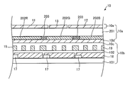
- FIG. 1 is a cross-sectional view illustrating a schematic configuration of a display device with a touch sensor according to an embodiment.
- FIG. 2 is a schematic view of the display device with a touch sensor shown in FIG. 1 as viewed from above.
- FIG. 3 is a schematic view of the display panel with a touch sensor shown in FIG. 1 as viewed from above.
- FIG. 4 is an enlarged schematic view of a part of the display panel with a touch sensor shown in FIG.
- FIG. 5 is a cross-sectional view taken along line AA in FIG.
- FIG. 6A is a diagram illustrating an alignment state of negative liquid crystal molecules.
- FIG. 6B is a diagram for explaining the alignment state of the liquid crystal molecules in Modification (2).
- FIG. 7 is a cross-sectional view showing a schematic configuration of a display panel with a touch sensor in Modification (3).
- a display device with a touch sensor includes an active matrix substrate having a common electrode and a pixel electrode, a counter substrate disposed to face the active matrix substrate, and the active matrix substrate and the counter A liquid crystal layer including liquid crystal molecules provided between the substrate and driven in response to a lateral electric field generated between the common electrode and the pixel electrode; and on a surface of the counter substrate opposite to the active matrix substrate.
- a touch sensor having a drive electrode and a detection electrode that are spaced apart in the horizontal direction, a dummy electrode that is disposed between the drive electrode and the detection electrode, and is in an electrically floating state, and the dummy electrode A shield electrode that is disposed in a region where the dummy electrode is disposed and is grounded between the liquid crystal layer and the liquid crystal layer.
- the display device with a touch sensor includes a liquid crystal layer between an active matrix substrate having a common electrode and a pixel electrode and a counter substrate.
- the liquid crystal layer includes liquid crystal molecules that are driven in accordance with a lateral electric field generated between the common electrode and the pixel electrode.
- a touch sensor having a drive electrode and a detection electrode spaced apart in the horizontal direction is formed on a surface of the counter substrate opposite to the active matrix substrate.
- the dummy electrode is disposed between the drive electrode and the detection electrode and is electrically floating.
- a grounded shield electrode is disposed between the counter substrate and the liquid crystal layer in a region where the dummy electrode is disposed.
- the electric field in the direction perpendicular to the substrate surface generated in the area where the dummy electrode is disposed is shielded by the shield electrode, and the liquid crystal layer Are less susceptible to this vertical electric field.
- the thickness of the device can be reduced as compared with the case where the shield electrode is provided on the counter substrate and the touch sensor is formed on the shield electrode through the insulating film, it is difficult to impair the design of the device.
- the counter substrate includes a color filter corresponding to a plurality of colors, and the shield electrode is provided between the color filter and the liquid crystal layer. Also good.
- the shield electrode may include a transparent conductive film in the first or second configuration.
- the third configuration it is possible to shield the electric field in the direction perpendicular to the substrate surface while reducing the decrease in the visibility of the display surface.
- the shield electrode in the first or second configuration, may include a mesh-like metal film.
- the fourth configuration it is possible to shield the electric field in the direction perpendicular to the substrate surface while reducing the decrease in the visibility of the display surface.
- the liquid crystal molecules may have negative dielectric anisotropy.
- the liquid crystal molecules are less likely to be affected by an electric field in the direction perpendicular to the substrate surface, so that abnormal alignment of liquid crystal molecules is less likely to occur.
- the liquid crystal molecules may have a positive dielectric anisotropy.
- the response speed is faster than in the case of using liquid crystal molecules having negative dielectric anisotropy, display quality can be improved.
- ⁇ dielectric anisotropy
- the liquid crystal molecules can be driven at a low voltage.
- FIG. 1 is a cross-sectional view showing a schematic configuration of a display device with a touch sensor according to the present embodiment.
- FIG. 2 is a schematic view of the display device with a touch sensor shown in FIG. 1 as viewed from above.
- the display device with a touch sensor 1 includes a display panel with a touch sensor 10, a backlight 20, a cover panel 30, a housing 40, and a bezel 50.
- the backlight 20 is disposed on the back side of the display panel 10 with a touch sensor, and irradiates the display panel 10 with a touch sensor with light.
- the cover panel 30 is disposed on the surface side of the display panel 10 with a touch sensor, and is made of a material excellent in impact resistance such as tempered glass.
- the display panel 10 with a touch sensor and the cover panel 30 are fixed and integrated with each other by a permeable adhesive.
- the housing 40 accommodates the backlight 20.
- the bezel 50 is attached to the housing 40 while supporting the display panel 10 with a touch sensor and the cover panel 30.
- FIG. 3 is a schematic view of the display panel 10 with a touch sensor as viewed from above.
- 4 is an enlarged schematic view of the broken-line frame portion shown in FIG. 3
- FIG. 5 is a cross-sectional view of the display panel with a touch sensor 10 taken along line AA shown in FIG.
- the display panel with a touch sensor 10 includes a color filter substrate (counter substrate) 10a, an active matrix substrate 10b, and a liquid crystal layer sandwiched between the color filter substrate 10a and the active matrix substrate 10b. 10c, a shield electrode 10d disposed between the liquid crystal layer 10c and the color filter substrate 10a, and a sensor unit 10e formed on the surface of the color filter substrate 10a.
- the active matrix substrate 10 b includes a plurality of thin film transistors (TFTs) 17 and a plurality of TFTs 17 on a surface of a substrate 101 having transparency such as glass (a surface on the liquid crystal layer 10 c side). And a plurality of pixel electrodes 18 connected to each other. A comb-like common electrode 19 having a plurality of openings is disposed on the TFT 17 and the pixel electrode 18 with an insulating film 102 interposed therebetween.
- alignment films for horizontally aligning liquid crystal molecules are provided on the surface of the active matrix substrate 10b on the liquid crystal layer 10c side and the surface of the color filter substrate 10a on the liquid crystal layer 10c side. That is, the alignment film is disposed between the common electrode 19 and the liquid crystal layer 10c and between the shield electrode 10d and the liquid crystal layer 10c.
- a transparent conductive film excellent in transparency and conductivity such as ITO (IndiumInTin Oxide) or ZnO (Zinc Oxide) is used.
- ITO IndiumInTin Oxide
- ZnO Zinc Oxide
- a voltage of ⁇ 1 v to 0 v is applied to the common electrode 19
- a voltage of 0 v to 5 v is applied to the pixel electrode 18, for example.
- the liquid crystal layer 10c includes, for example, liquid crystal molecules having negative dielectric anisotropy (negative type).
- a lateral electric field (fringe field) is generated between the pixel electrode 18 and the common electrode 19 in the opening of the common electrode 19.
- the negative liquid crystal molecules are driven in the horizontal direction with respect to the substrate 101 in accordance with the lateral electric field.
- the negative liquid crystal molecules rotate so that the minor axis direction thereof is in the direction of the generated transverse electric field, that is, the major axis direction of the liquid crystal molecules is oriented in the direction perpendicular to the electric field.
- the color filter substrate 10a has R (red), G (green), and B (blue) at positions corresponding to the pixel electrodes 18 on the back surface (surface on the liquid crystal layer 10c side) of the transparent substrate 201 such as glass.
- Color filters 202R, 202G, and 202B corresponding to the respective colors are provided.
- the color filter substrate 10 a is provided with a black matrix 203 between adjacent color filters 202.
- the region where the R, G, B color filters 202R, 202G, 202B are arranged constitutes one sub-pixel, and one pixel is constituted by these three sub-pixels.
- a grounded shield electrode 10d is provided between the color filter 202 and the black matrix 203 and the liquid crystal layer 10c. More specifically, the shield electrode 10d is provided between the color filter 202 and the black matrix 203 and an alignment film (not shown) provided on the side of the color filter substrate 10a sandwiching the liquid crystal layer 10c. In this example, the distance between the shield electrode 10d and the common electrode 19 below the shield electrode 10d is about 3 ⁇ m.
- the material of the shield electrode 10d for example, a transparent conductive film such as ITO is used, and the film thickness is preferably about 10 nm, for example.
- the sheet resistance of the shield electrode 10d is preferably 1 k ⁇ / ⁇ or less. The lower the resistance between the shield electrode 10d and the ground (GND), the more the electric field perpendicular to the substrate surface is shielded by the shield electrode 10d. If the resistance between the shield electrode 10d and the ground (GND) is 1 k ⁇ / ⁇ or less, a vertical electric field due to the approach of a charged body up to about 10 kV can be shielded by the shield electrode 10d.
- the shield electrode 10d includes the dummy electrode 13, the liquid crystal layer 10c, and the like. It suffices to be provided so as to overlap at least the dummy electrode 13.
- the sensor unit 10 e includes a drive electrode 11, a detection electrode 12, and a dummy electrode 13. As shown in FIG. 3, drive electrodes 11 are arranged along the Y-axis direction on the surface of the color filter substrate 10a of the display panel 10 with a touch sensor.
- the drive electrode 11 includes a plurality of drive electrode pads 11a to 11m arranged in the Y-axis direction.
- a plurality of drive electrodes 11 are provided in the X-axis direction at a predetermined interval.
- the detection electrode 12 is a continuous electrode extended in the Y-axis direction.
- a plurality of detection electrodes 12 are provided in the X-axis direction at a predetermined interval.
- a transparent conductive film having excellent transparency and conductivity such as ITO or ZnO, is used.
- the drive electrode 11 is connected via a wiring 14 to a touch detection circuit (not shown) for controlling the detection of the touch position.
- the drive electrode 11 is supplied with a drive signal for detecting a touch position via a wiring 14 from a touch detection circuit (not shown).
- the detection electrode 12 is connected to a touch detection circuit (not shown), and outputs a signal corresponding to the capacitance between the detection electrode 12 and the drive electrode 11 to the touch detection circuit (not shown).
- the touch position is detected as follows.
- a drive signal is supplied from the touch detection circuit (not shown) to the drive electrode 11 to scan the drive electrode 11, and a signal indicating the capacitance between the drive electrode 11 and the detection electrode 12 is output from the detection electrode 12 to the touch detection circuit. (Not shown).
- the capacitance between the drive electrode 11 and the detection electrode 12 at the contact position changes.
- the touch detection circuit detects a touch position based on a capacitance in a state where the charged body is not approaching the display surface and a signal indicating the capacitance output from the detection electrode 12.
- dummy electrodes 13 are provided in regions other than the region where the drive electrode 11, the detection electrode 12, and the wiring 14 are provided.
- the dummy electrode 13 is provided in order to prevent occurrence of luminance unevenness due to a difference in transmittance between a region where the drive electrode 11, the detection electrode 12, and the wiring 14 are provided and a region other than this region.
- a transparent conductive film such as ITO or ZnO is used as in the drive electrode 11 and the detection electrode 12.
- the dummy electrode 13 is not connected to any of the drive electrode 11, the detection electrode 12, and the wiring 14, and is disposed in an electrically floating state.
- the shield electrode 10d is provided between the liquid crystal layer 10c and the color filter substrate 10a, the charged body approaches the region where the dummy electrode 13 is disposed. Even so, the vertical electric field is shielded by the shield electrode 10d. As a result, a vertical electric field is not generated between the dummy electrode 13 and the common electrode 19, and the alignment of the liquid crystal molecules in the liquid crystal layer 10c is not disturbed, so that display defects can be prevented.
- the shield electrode 10d is formed between the color filter substrate 10a and the liquid crystal layer 10c, and the touch sensor (the drive electrode 11 and the detection electrode 12) is formed on the surface of the color filter substrate 10a. .
- the thickness of the display panel 10 with a touch sensor can be reduced compared to the case where a shield electrode is provided on the color filter substrate 10a and the touch sensor is formed via an insulating film. .
- the shield electrode 10d is configured using a transparent conductive film.
- the shield electrode 10d is configured using, for example, a metal film formed in a mesh shape. Also good. For example, Cu, Al, Ta, or the like may be used as the material of the metal film.
- the liquid crystal layer 10c includes liquid crystal molecules (positive type) having positive dielectric anisotropy. May be.
- the shield electrode 10d is not provided, when a vertical electric field is generated in the region where the dummy electrode 13 is arranged, the liquid crystal molecules are aligned so that the major axis direction of the liquid crystal molecule is directed to the direction of the vertical electric field. .
- the pixel in which the liquid crystal molecules are arranged has a display defect.
- the shield electrode 10d is provided.
- FIGS. 6A and 6B are schematic diagrams illustrating the alignment state of negative liquid crystal molecules and positive liquid crystal molecules in a region where the shield electrode 10d is provided.
- the color filter substrate 10a and the sensor unit 10e are not shown, but the color filter substrate 10a and the sensor unit 10e are arranged on the shield electrode 10d as in FIG.
- a fringe electric field (broken line) is generated between the shield electrode 10 d and the pixel electrode 18.
- the liquid crystal molecules 101c are aligned in a substantially horizontal direction with respect to the substrate surface because the short axes are aligned along the fringe electric field.
- the liquid crystal molecules 102c are aligned so that the major axis direction thereof is oriented along the fringe electric field between the shield electrode 10d and the pixel electrode 18. That is, since the positive liquid crystal molecule 102c is more susceptible to the electric field in the direction perpendicular to the substrate surface than the negative liquid crystal molecule 101c, the liquid crystal molecule 102c is provided even if the shield electrode 10d is provided. The orientation of fluctuates in the vertical direction.
- FIG. 7 is an enlarged cross-sectional view of one sub-pixel portion of the display panel with a touch sensor 10 shown in FIG.
- a comb-like pixel electrode 181 and a common electrode 191 are provided on a substrate 101.
- the pixel electrodes 181 and the common electrodes 191 are alternately arranged with a horizontal separation with respect to the substrate surface.
- the liquid crystal molecules in the liquid crystal layer 10c are driven according to the lateral electric field generated between the adjacent pixel electrode 181 and the common electrode 191.
- the shield electrode 10d when a vertical electric field is generated between the dummy electrode 13 and the pixel electrode 181 or the common electrode 191 in the region where the dummy electrode 13 (see FIG. 5) is disposed, the shield electrode 10d The electric field in the vertical direction is shielded, and abnormal alignment of the liquid crystal layer 10c can be suppressed.
- the liquid crystal molecules in the liquid crystal layer 10c may be a positive type or a negative type.
- SYMBOLS 1 Display apparatus with a touch sensor, 10 ... Display panel with a touch sensor, 10a ... Color filter substrate, 10b ... Active matrix substrate, 10c ... Liquid crystal layer, 10e ... Sensor part, 10d ... Shield electrode, 11 ... Drive electrode, 11a- 11 m: drive electrode pad, 12: detection electrode, 13: dummy electrode, 14: wiring, 17: TFT, 18, 181: pixel electrode 18, 191 ... common electrode, 101, 201 ... substrate, 202 ... color filter, 203 ... Black matrix
Landscapes
- Physics & Mathematics (AREA)
- Engineering & Computer Science (AREA)
- Nonlinear Science (AREA)
- General Physics & Mathematics (AREA)
- General Engineering & Computer Science (AREA)
- Theoretical Computer Science (AREA)
- Chemical & Material Sciences (AREA)
- Crystallography & Structural Chemistry (AREA)
- Optics & Photonics (AREA)
- Human Computer Interaction (AREA)
- Mathematical Physics (AREA)
- Liquid Crystal (AREA)
- Microelectronics & Electronic Packaging (AREA)
Abstract
Provided is a technique for reducing display defects caused by an electric field in a direction perpendicular to an in-plane-switching liquid crystal display panel without compromising the design properties of a display device equipped with a touch sensor, in which a touch sensor is formed in the display panel. A display device equipped with a touch sensor is provided with an active-matrix substrate 10b having pixel electrodes 18 and shared electrodes 19, a color filter substrate 10a, and a liquid crystal layer 10c driven by transverse electric fields generated between the pixel electrodes 18 and the shared electrodes 19. A touch sensor having a drive electrodes 11 and detection electrodes 12 arranged so as to be separated from each other in the horizontal direction is provided to the reverse side of the color filter substrate 10a from the active-matrix substrate 10b, and dummy electrodes 13 in an electrically floating state are provided between the drive electrodes 11 and the detection electrodes 12. A grounded shield electrode 10d is provided between the dummy electrodes 13 and the liquid crystal layer 10c.
Description
本発明は、タッチセンサ付き表示装置に関する。
The present invention relates to a display device with a touch sensor.
下記特許文献1には、横電界方式の液晶パネルの観察方向側にタッチパネルを配置した液晶表示装置において、液晶パネルにおける対向基板とタッチパネルとの間に、接地されたシールド導電層を設ける技術が開示されている。特許文献1では、タッチパネルと対向基板との間に、接地されたシールド導電層を設けることで、外部からの電磁ノイズが液晶に入り込むことによる表示不良を防止している。
Patent Document 1 below discloses a technique in which a grounded shield conductive layer is provided between a counter substrate and a touch panel in a liquid crystal panel in a liquid crystal display device in which a touch panel is arranged on the observation direction side of a horizontal electric field type liquid crystal panel. Has been. In Patent Document 1, a grounded shield conductive layer is provided between the touch panel and the counter substrate, thereby preventing display defects caused by external electromagnetic noise entering the liquid crystal.
タッチセンサ付き表示装置としては、横電界方式の液晶パネルにおける対向基板上にタッチセンサのセンサパターンが形成されたものがある。このようなタッチセンサ付き表示装置において、対向基板上のセンサパターンが形成されていない領域に、電気的にフローティングされたダミー電極が形成される場合がある。ダミー電極は、センサパターンが形成された領域とセンサパターンが形成されていない領域の透過率を調整するために設けられる。ダミー電極が形成された領域に帯電体が接近すると、液晶パネルのアクティブマトリクス基板における電極とダミー電極との間に生じる垂直方向の電界によって液晶分子が異常配向し、表示不良が発生する。
As a display device with a touch sensor, there is one in which a sensor pattern of a touch sensor is formed on a counter substrate in a horizontal electric field type liquid crystal panel. In such a display device with a touch sensor, an electrically floating dummy electrode may be formed in a region where the sensor pattern on the counter substrate is not formed. The dummy electrode is provided to adjust the transmittance between the region where the sensor pattern is formed and the region where the sensor pattern is not formed. When the charged body approaches the area where the dummy electrode is formed, the liquid crystal molecules are abnormally oriented due to a vertical electric field generated between the electrode and the dummy electrode in the active matrix substrate of the liquid crystal panel, and display defects occur.
タッチセンサのセンサパターンが対向基板上に形成されたタッチセンサ付き表示装置においても、上記特許文献1のように、シールド導電層を対向基板上に設ける場合、シールド導電層の上に絶縁膜を介してセンサパターンを形成しなければならない。その結果、装置の厚みが増し、装置のデザイン性に影響を及ぼす。
Also in the display device with a touch sensor in which the sensor pattern of the touch sensor is formed on the counter substrate, when the shield conductive layer is provided on the counter substrate as in Patent Document 1, an insulating film is interposed on the shield conductive layer. The sensor pattern must be formed. As a result, the thickness of the device increases, which affects the design of the device.
本発明は、横電界方式の液晶表示パネルにタッチセンサが形成されたタッチセンサ付き表示装置において、装置のデザイン性を損なうことなく、液晶表示パネルに対する垂直方向の電界によって生じる表示不良を軽減する技術を提供することを目的とする。
The present invention relates to a display device with a touch sensor in which a touch sensor is formed on a horizontal electric field type liquid crystal display panel, and a technique for reducing display defects caused by an electric field in the vertical direction with respect to the liquid crystal display panel without impairing the design of the device. The purpose is to provide.
本発明に係るタッチセンサ付き表示装置は、共通電極と画素電極とを有するアクティブマトリクス基板と、前記アクティブマトリクス基板に対向して配置された対向基板と、前記アクティブマトリクス基板と前記対向基板との間に設けられ、前記共通電極と前記画素電極との間に生じる横電界に応じて駆動する液晶分子を含む液晶層と、前記対向基板において前記アクティブマトリクス基板とは反対側の面に、水平方向に離間して配置された駆動電極及び検出電極を有するタッチセンサと、前記駆動電極と前記検出電極との間に配置され、電気的にフローティング状態のダミー電極と、前記ダミー電極と前記液晶層との間において、前記ダミー電極が配置され、接地された領域に配置されたシールド電極と、を備える。
A display device with a touch sensor according to the present invention includes an active matrix substrate having a common electrode and a pixel electrode, a counter substrate disposed to face the active matrix substrate, and a space between the active matrix substrate and the counter substrate. A liquid crystal layer including liquid crystal molecules that are driven according to a lateral electric field generated between the common electrode and the pixel electrode, and a surface opposite to the active matrix substrate in the counter substrate in a horizontal direction. A touch sensor having a drive electrode and a detection electrode arranged apart from each other, a dummy electrode placed between the drive electrode and the detection electrode and electrically floating, and the dummy electrode and the liquid crystal layer In the meantime, the dummy electrode is disposed, and a shield electrode is disposed in a grounded region.
本発明の構成によれば、横電界方式の液晶表示パネルにタッチセンサが形成されたタッチセンサ付き表示装置において、装置のデザイン性を損なうことなく、液晶表示パネルに対する垂直方向の電界によって生じる表示不良を軽減することができる。
According to the configuration of the present invention, in a display device with a touch sensor in which a touch sensor is formed on a horizontal electric field type liquid crystal display panel, a display defect caused by an electric field in a vertical direction with respect to the liquid crystal display panel without impairing the design of the device. Can be reduced.
本発明の一実施形態に係るタッチセンサ付き表示装置は、共通電極と画素電極とを有するアクティブマトリクス基板と、前記アクティブマトリクス基板に対向して配置された対向基板と、前記アクティブマトリクス基板と前記対向基板との間に設けられ、前記共通電極と前記画素電極との間に生じる横電界に応じて駆動する液晶分子を含む液晶層と、前記対向基板において前記アクティブマトリクス基板とは反対側の面に、水平方向に離間して配置された駆動電極及び検出電極を有するタッチセンサと、前記駆動電極と前記検出電極との間に配置され、電気的にフローティング状態のダミー電極と、前記ダミー電極と前記液晶層との間において、前記ダミー電極が配置された領域に配置され、接地されたシールド電極と、を備える(第1の構成)。
A display device with a touch sensor according to an embodiment of the present invention includes an active matrix substrate having a common electrode and a pixel electrode, a counter substrate disposed to face the active matrix substrate, and the active matrix substrate and the counter A liquid crystal layer including liquid crystal molecules provided between the substrate and driven in response to a lateral electric field generated between the common electrode and the pixel electrode; and on a surface of the counter substrate opposite to the active matrix substrate. A touch sensor having a drive electrode and a detection electrode that are spaced apart in the horizontal direction, a dummy electrode that is disposed between the drive electrode and the detection electrode, and is in an electrically floating state, and the dummy electrode A shield electrode that is disposed in a region where the dummy electrode is disposed and is grounded between the liquid crystal layer and the liquid crystal layer. Adult).
第1の構成によれば、タッチセンサ付き表示装置は、共通電極と画素電極とを有するアクティブマトリクス基板と、対向基板との間に液晶層を備える。液晶層は、共通電極と画素電極との間に生じる横電界に応じて駆動する液晶分子を含む。対向基板のアクティブマトリクス基板と反対側の面には、水平方向に離間して配置された駆動電極と検出電極とを有するタッチセンサが形成されている。ダミー電極は、駆動電極と検出電極との間に配置され、電気的にフローティングされている。対向基板と液晶層との間には、ダミー電極が配置された領域に、接地されたシールド電極が配置されている。そのため、ダミー電極が配置された領域に指等の帯電体が接近した場合であっても、ダミー電極が配置された領域に生じる、基板面に対する垂直方向の電界がシールド電極によって遮蔽され、液晶層はこの垂直方向の電界の影響を受けにくい。その結果、垂直方向の電界による液晶層の異常配向が抑制され、表示不良を軽減することができる。また、対向基板上にシールド電極を設け、絶縁膜を介してタッチセンサをシールド電極上に形成する場合と比べ、装置の厚みを薄くすることができるので、装置のデザイン性を損ないにくい。
According to the first configuration, the display device with a touch sensor includes a liquid crystal layer between an active matrix substrate having a common electrode and a pixel electrode and a counter substrate. The liquid crystal layer includes liquid crystal molecules that are driven in accordance with a lateral electric field generated between the common electrode and the pixel electrode. A touch sensor having a drive electrode and a detection electrode spaced apart in the horizontal direction is formed on a surface of the counter substrate opposite to the active matrix substrate. The dummy electrode is disposed between the drive electrode and the detection electrode and is electrically floating. A grounded shield electrode is disposed between the counter substrate and the liquid crystal layer in a region where the dummy electrode is disposed. Therefore, even when a charged body such as a finger approaches the area where the dummy electrode is disposed, the electric field in the direction perpendicular to the substrate surface generated in the area where the dummy electrode is disposed is shielded by the shield electrode, and the liquid crystal layer Are less susceptible to this vertical electric field. As a result, abnormal alignment of the liquid crystal layer due to a vertical electric field is suppressed, and display defects can be reduced. In addition, since the thickness of the device can be reduced as compared with the case where the shield electrode is provided on the counter substrate and the touch sensor is formed on the shield electrode through the insulating film, it is difficult to impair the design of the device.
第2の構成は、第1の構成において、前記対向基板は、複数の色に対応するカラーフィルタを備え、前記シールド電極は、前記カラーフィルタと前記液晶層との間に設けられていることとしてもよい。
According to a second configuration, in the first configuration, the counter substrate includes a color filter corresponding to a plurality of colors, and the shield electrode is provided between the color filter and the liquid crystal layer. Also good.
第3の構成は、第1又は第2の構成において、前記シールド電極は、透明導電膜を含むこととしてもよい。
In a third configuration, the shield electrode may include a transparent conductive film in the first or second configuration.
第3の構成によれば、表示面の視認性の低下を軽減しつつ、基板面に対する垂直方向の電界を遮蔽することができる。
According to the third configuration, it is possible to shield the electric field in the direction perpendicular to the substrate surface while reducing the decrease in the visibility of the display surface.
第4の構成は、第1又は第2の構成において、前記シールド電極は、メッシュ状の金属膜を含むこととしてもよい。
According to a fourth configuration, in the first or second configuration, the shield electrode may include a mesh-like metal film.
第4の構成によれば、表示面の視認性の低下を軽減しつつ、基板面に対する垂直方向の電界を遮蔽することができる。
According to the fourth configuration, it is possible to shield the electric field in the direction perpendicular to the substrate surface while reducing the decrease in the visibility of the display surface.
第5の構成は、第1から第4のいずれかの構成において、前記液晶分子は、負の誘電率異方性を有することとしてもよい。
In the fifth configuration, in any one of the first to fourth configurations, the liquid crystal molecules may have negative dielectric anisotropy.
第5の構成によれば、正の誘電率異方性を有する液晶分子と比べ、基板面に対する垂直方向の電界の影響を受けにくいため、液晶分子の異常配向を生じにくい。
According to the fifth configuration, compared with liquid crystal molecules having a positive dielectric anisotropy, the liquid crystal molecules are less likely to be affected by an electric field in the direction perpendicular to the substrate surface, so that abnormal alignment of liquid crystal molecules is less likely to occur.
第6の構成は、第1から第4のいずれかの構成において、前記液晶分子は、正の誘電率異方性を有することとしてもよい。
In a sixth configuration, in any one of the first to fourth configurations, the liquid crystal molecules may have a positive dielectric anisotropy.
第6の構成によれば、負の誘電率異方性を有する液晶分子を用いる場合と比べて応答速度が速いため、表示品質を向上させることができる。また、負の誘電率異方性を有する液晶分子を用いる場合と比べて、Δε(誘電率異方性)が大きいため低電圧で液晶分子を駆動することができる。
According to the sixth configuration, since the response speed is faster than in the case of using liquid crystal molecules having negative dielectric anisotropy, display quality can be improved. In addition, since Δε (dielectric anisotropy) is large compared to the case of using liquid crystal molecules having negative dielectric anisotropy, the liquid crystal molecules can be driven at a low voltage.
以下、図面を参照し、本発明の実施の形態を詳しく説明する。図中同一又は相当部分には同一符号を付してその説明は繰り返さない。
Hereinafter, embodiments of the present invention will be described in detail with reference to the drawings. In the drawings, the same or corresponding parts are denoted by the same reference numerals and description thereof will not be repeated.
図1は、本実施の形態に係るタッチセンサ付き表示装置の概略構成を示す断面図である。図2は、図1に示すタッチセンサ付き表示装置を上から見た模式図である。
FIG. 1 is a cross-sectional view showing a schematic configuration of a display device with a touch sensor according to the present embodiment. FIG. 2 is a schematic view of the display device with a touch sensor shown in FIG. 1 as viewed from above.
図1及び図2に示すように、タッチセンサ付き表示装置1は、タッチセンサ付き表示パネル10と、バックライト20と、カバーパネル30と、筐体40と、ベゼル50とを含む。
As shown in FIGS. 1 and 2, the display device with a touch sensor 1 includes a display panel with a touch sensor 10, a backlight 20, a cover panel 30, a housing 40, and a bezel 50.
バックライト20は、タッチセンサ付き表示パネル10の裏面側に配置され、タッチセンサ付き表示パネル10に光を照射する。
The backlight 20 is disposed on the back side of the display panel 10 with a touch sensor, and irradiates the display panel 10 with a touch sensor with light.
カバーパネル30は、タッチセンサ付き表示パネル10の表面側に配置され、例えば強化ガラスなどの耐衝撃性能に優れた材料からなる。
The cover panel 30 is disposed on the surface side of the display panel 10 with a touch sensor, and is made of a material excellent in impact resistance such as tempered glass.
タッチセンサ付き表示パネル10とカバーパネル30は、それぞれの間に透過性を有する接着剤によって相互に固着され、一体化されている。
The display panel 10 with a touch sensor and the cover panel 30 are fixed and integrated with each other by a permeable adhesive.
筐体40は、バックライト20を収容する。
The housing 40 accommodates the backlight 20.
ベゼル50は、タッチセンサ付き表示パネル10とカバーパネル30を支持して、筐体40に取り付けられている。
The bezel 50 is attached to the housing 40 while supporting the display panel 10 with a touch sensor and the cover panel 30.
図3は、タッチセンサ付き表示パネル10を上から見た模式図である。また、図4は、図3に示す破線枠部分を拡大した模式図であり、図5は、図4に示すA-A線でタッチセンサ付き表示パネル10を切断した断面図である。
FIG. 3 is a schematic view of the display panel 10 with a touch sensor as viewed from above. 4 is an enlarged schematic view of the broken-line frame portion shown in FIG. 3, and FIG. 5 is a cross-sectional view of the display panel with a touch sensor 10 taken along line AA shown in FIG.
図3~図5に示すように、タッチセンサ付き表示パネル10は、カラーフィルタ基板(対向基板)10a、アクティブマトリクス基板10b、カラーフィルタ基板10aとアクティブマトリクス基板10bとの間に挟持された液晶層10c、液晶層10cとカラーフィルタ基板10aとの間に配置されたシールド電極10d、及び、カラーフィルタ基板10aの表面に形成されたセンサ部10eを備える。
As shown in FIGS. 3 to 5, the display panel with a touch sensor 10 includes a color filter substrate (counter substrate) 10a, an active matrix substrate 10b, and a liquid crystal layer sandwiched between the color filter substrate 10a and the active matrix substrate 10b. 10c, a shield electrode 10d disposed between the liquid crystal layer 10c and the color filter substrate 10a, and a sensor unit 10e formed on the surface of the color filter substrate 10a.
図5に示すように、アクティブマトリクス基板10bは、ガラス等の透過性を有する基板101の表面(液晶層10c側の面)に、複数の薄膜トランジスタ(TFT:Thin Film Transistor)17と、複数のTFT17と接続された複数の画素電極18とを備える。TFT17及び画素電極18の上には、絶縁膜102を介して複数の開口部を有する櫛歯状の共通電極19が配置されている。なお、図示を省略するが、アクティブマトリクス基板10bの液晶層10c側の面とカラーフィルタ基板10aの液晶層10c側の面に、液晶分子を水平配向させるための配向膜が設けられている。つまり、配向膜は、共通電極19と液晶層10cとの間、及び、シールド電極10dと液晶層10cとの間にそれぞれ配置されている。
As shown in FIG. 5, the active matrix substrate 10 b includes a plurality of thin film transistors (TFTs) 17 and a plurality of TFTs 17 on a surface of a substrate 101 having transparency such as glass (a surface on the liquid crystal layer 10 c side). And a plurality of pixel electrodes 18 connected to each other. A comb-like common electrode 19 having a plurality of openings is disposed on the TFT 17 and the pixel electrode 18 with an insulating film 102 interposed therebetween. Although not shown, alignment films for horizontally aligning liquid crystal molecules are provided on the surface of the active matrix substrate 10b on the liquid crystal layer 10c side and the surface of the color filter substrate 10a on the liquid crystal layer 10c side. That is, the alignment film is disposed between the common electrode 19 and the liquid crystal layer 10c and between the shield electrode 10d and the liquid crystal layer 10c.
画素電極18及び共通電極19としては、ITO(Indium Tin Oxide)又はZnO(Zinc Oxide)等、透過性及び導電性に優れた透明導電膜が用いられる。共通電極19は、例えば、-1v~0vの電圧が印加され、画素電極18は、例えば、0v~5vの電圧が印加される。
As the pixel electrode 18 and the common electrode 19, a transparent conductive film excellent in transparency and conductivity, such as ITO (IndiumInTin Oxide) or ZnO (Zinc Oxide), is used. For example, a voltage of −1 v to 0 v is applied to the common electrode 19, and a voltage of 0 v to 5 v is applied to the pixel electrode 18, for example.
液晶層10cは、本実施の形態では、例えば、負の誘電率異方性(ネガ型)を有する液晶分子を含む。共通電極19の開口部において、画素電極18と共通電極19との間に横電界(フリンジ電界)が生じる。ネガ型の液晶分子は、この横電界に応じて、基板101に対して水平方向に駆動される。ネガ型の液晶分子は、発生した横電界の方向にその短軸方向が向くように、すなわち、電界に垂直な方向に液晶分子の長軸方向が向くように回転する。
In the present embodiment, the liquid crystal layer 10c includes, for example, liquid crystal molecules having negative dielectric anisotropy (negative type). A lateral electric field (fringe field) is generated between the pixel electrode 18 and the common electrode 19 in the opening of the common electrode 19. The negative liquid crystal molecules are driven in the horizontal direction with respect to the substrate 101 in accordance with the lateral electric field. The negative liquid crystal molecules rotate so that the minor axis direction thereof is in the direction of the generated transverse electric field, that is, the major axis direction of the liquid crystal molecules is oriented in the direction perpendicular to the electric field.
カラーフィルタ基板10aは、ガラス等の透過性を有する基板201の裏面(液晶層10c側の面)において、画素電極18に対応する位置に、R(赤)、G(緑)、B(青)の各色に対応するカラーフィルタ202R、202G、202Bを備える。また、カラーフィルタ基板10aには、隣接するカラーフィルタ202の間にブラックマトリクス203が設けられている。
The color filter substrate 10a has R (red), G (green), and B (blue) at positions corresponding to the pixel electrodes 18 on the back surface (surface on the liquid crystal layer 10c side) of the transparent substrate 201 such as glass. Color filters 202R, 202G, and 202B corresponding to the respective colors are provided. The color filter substrate 10 a is provided with a black matrix 203 between adjacent color filters 202.
R,G,Bのカラーフィルタ202R、202G、202Bが配置された領域が1つのサブ画素を構成しており、これら3つのサブ画素によって1つの画素が構成されている。
The region where the R, G, B color filters 202R, 202G, 202B are arranged constitutes one sub-pixel, and one pixel is constituted by these three sub-pixels.
カラーフィルタ202及びブラックマトリクス203と液晶層10cとの間には、接地されたシールド電極10dが設けられている。より具体的には、シールド電極10dは、カラーフィルタ202及びブラックマトリクス203と、液晶層10cを挟むカラーフィルタ基板10aの側に設けられた配向膜(図示略)との間に設けられている。この例において、シールド電極10dと、シールド電極10dの下側の共通電極19の間の距離は3μm程度である。
Between the color filter 202 and the black matrix 203 and the liquid crystal layer 10c, a grounded shield electrode 10d is provided. More specifically, the shield electrode 10d is provided between the color filter 202 and the black matrix 203 and an alignment film (not shown) provided on the side of the color filter substrate 10a sandwiching the liquid crystal layer 10c. In this example, the distance between the shield electrode 10d and the common electrode 19 below the shield electrode 10d is about 3 μm.
シールド電極10dの材料としては、例えば、ITO等の透明導電膜が用いられ、その膜厚は、例えば10nm程度が好ましい。また、シールド電極10dの面抵抗は、1kΩ/□以下が好ましい。シールド電極10dとグランド(GND)との間の抵抗が低いほど、基板面に対する垂直方向の電界がシールド電極10dによって遮蔽される。シールド電極10dとグランド(GND)との間の抵抗が1kΩ/□以下であれば、10kV程度までの帯電体の接近による垂直電界をシールド電極10dによって遮蔽することができる。
As the material of the shield electrode 10d, for example, a transparent conductive film such as ITO is used, and the film thickness is preferably about 10 nm, for example. The sheet resistance of the shield electrode 10d is preferably 1 kΩ / □ or less. The lower the resistance between the shield electrode 10d and the ground (GND), the more the electric field perpendicular to the substrate surface is shielded by the shield electrode 10d. If the resistance between the shield electrode 10d and the ground (GND) is 1 kΩ / □ or less, a vertical electric field due to the approach of a charged body up to about 10 kV can be shielded by the shield electrode 10d.
なお、本実施の形態は、後述するセンサ部10eにおけるダミー電極13が配置されていない領域にもシールド電極10dが設けられる例を説明するが、シールド電極10dは、ダミー電極13と液晶層10cとの間において、少なくともダミー電極13と重なるように設けられていればよい。
In the present embodiment, an example in which the shield electrode 10d is provided in a region where the dummy electrode 13 is not disposed in the sensor unit 10e described later will be described. The shield electrode 10d includes the dummy electrode 13, the liquid crystal layer 10c, and the like. It suffices to be provided so as to overlap at least the dummy electrode 13.
センサ部10eは、駆動電極11、検出電極12、及びダミー電極13を含む。図3に示すように、タッチセンサ付き表示パネル10のカラーフィルタ基板10aの表面には、Y軸方向に沿って駆動電極11が配置されている。駆動電極11は、Y軸方向に配列された複数の駆動用電極パッド11a~11mを含む。駆動電極11は、所定の間隔を隔ててX軸方向に複数設けられている。また、検出電極12は、Y軸方向に延伸された1つながりの電極である。検出電極12は、所定の間隔を隔ててX軸方向に複数設けられている。
The sensor unit 10 e includes a drive electrode 11, a detection electrode 12, and a dummy electrode 13. As shown in FIG. 3, drive electrodes 11 are arranged along the Y-axis direction on the surface of the color filter substrate 10a of the display panel 10 with a touch sensor. The drive electrode 11 includes a plurality of drive electrode pads 11a to 11m arranged in the Y-axis direction. A plurality of drive electrodes 11 are provided in the X-axis direction at a predetermined interval. Further, the detection electrode 12 is a continuous electrode extended in the Y-axis direction. A plurality of detection electrodes 12 are provided in the X-axis direction at a predetermined interval.
駆動電極11及び検出電極12の材料としては、例えばITO又はZnO等、透過性及び導電性に優れた透明導電膜が用いられる。
As the material of the drive electrode 11 and the detection electrode 12, a transparent conductive film having excellent transparency and conductivity, such as ITO or ZnO, is used.
駆動電極11は、配線14を介して、タッチ位置の検出を制御するためのタッチ検出回路(図示略)と接続されている。駆動電極11は、タッチ検出回路(図示略)から配線14を介してタッチ位置を検出するための駆動信号が供給される。検出電極12は、タッチ検出回路(図示略)と接続され、駆動電極11との間の静電容量に応じた信号をタッチ検出回路(図示略)に出力する。
The drive electrode 11 is connected via a wiring 14 to a touch detection circuit (not shown) for controlling the detection of the touch position. The drive electrode 11 is supplied with a drive signal for detecting a touch position via a wiring 14 from a touch detection circuit (not shown). The detection electrode 12 is connected to a touch detection circuit (not shown), and outputs a signal corresponding to the capacitance between the detection electrode 12 and the drive electrode 11 to the touch detection circuit (not shown).
タッチ位置の検出は以下のようにして行う。タッチ検出回路(図示略)から駆動電極11に駆動信号を供給して駆動電極11を走査し、駆動電極11と検出電極12との間の静電容量を示す信号が検出電極12からタッチ検出回路(図示略)に出力される。タッチセンサ付き表示装置1の表示面に指等の帯電体が接近すると、接触位置における駆動電極11と検出電極12との間の静電容量が変化する。タッチ検出回路(図示略)は、表示面に帯電体が接近していない状態の静電容量と、検出電極12から出力される静電容量を示す信号とに基づいてタッチ位置を検出する。
The touch position is detected as follows. A drive signal is supplied from the touch detection circuit (not shown) to the drive electrode 11 to scan the drive electrode 11, and a signal indicating the capacitance between the drive electrode 11 and the detection electrode 12 is output from the detection electrode 12 to the touch detection circuit. (Not shown). When a charged body such as a finger approaches the display surface of the display device 1 with a touch sensor, the capacitance between the drive electrode 11 and the detection electrode 12 at the contact position changes. The touch detection circuit (not shown) detects a touch position based on a capacitance in a state where the charged body is not approaching the display surface and a signal indicating the capacitance output from the detection electrode 12.
また、図3及び図4に示すように、駆動電極11、検出電極12、及び配線14が設けられた領域以外の領域にはダミー電極13が設けられている。ダミー電極13は、駆動電極11、検出電極12、及び配線14が設けられた領域と、この領域以外の領域との透過率の差による輝度むらの発生を防止するために設けられている。ダミー電極13の材料は、駆動電極11及び検出電極12と同様、ITO又はZnO等の透明導電膜が用いられている。ダミー電極13は、駆動電極11、検出電極12、及び配線14のいずれにも接続されておらず、電気的にフローティングされた状態で配置されている。
Further, as shown in FIGS. 3 and 4, dummy electrodes 13 are provided in regions other than the region where the drive electrode 11, the detection electrode 12, and the wiring 14 are provided. The dummy electrode 13 is provided in order to prevent occurrence of luminance unevenness due to a difference in transmittance between a region where the drive electrode 11, the detection electrode 12, and the wiring 14 are provided and a region other than this region. As the material of the dummy electrode 13, a transparent conductive film such as ITO or ZnO is used as in the drive electrode 11 and the detection electrode 12. The dummy electrode 13 is not connected to any of the drive electrode 11, the detection electrode 12, and the wiring 14, and is disposed in an electrically floating state.
ダミー電極13が配置された領域に帯電体が接近した場合、ダミー電極13が配置された領域において、基板面に対して垂直方向の電界が発生する。液晶層10cとカラーフィルタ基板10aとの間にシールド電極10dが設けられていない場合、ダミー電極13と共通電極19との間に電界が生じ、液晶層10cの液晶分子の一端が水平面から浮き上がったり、液晶分子が水平面で回転したりする等、液晶分子の異常配向が生じる。その結果、例えば、本来、黒色を表示させる画素が白っぽく表示されたり、白色を表示させる画素がグレーがかって表示されたりする。
When the charged body approaches the area where the dummy electrode 13 is disposed, an electric field perpendicular to the substrate surface is generated in the area where the dummy electrode 13 is disposed. When the shield electrode 10d is not provided between the liquid crystal layer 10c and the color filter substrate 10a, an electric field is generated between the dummy electrode 13 and the common electrode 19, and one end of the liquid crystal molecules of the liquid crystal layer 10c is lifted from the horizontal plane. An abnormal alignment of the liquid crystal molecules occurs, for example, the liquid crystal molecules rotate on a horizontal plane. As a result, for example, pixels that originally display black are displayed whitish, or pixels that display white are displayed in gray.
本実施の形態では、図5に示すように、液晶層10cとカラーフィルタ基板10aとの間にシールド電極10dが設けられているため、ダミー電極13が配置された領域に帯電体が接近した場合であっても、シールド電極10dによって垂直方向の電界が遮蔽される。その結果、ダミー電極13と共通電極19との間に垂直電界が生じず、液晶層10cの液晶分子の配向が乱れないため、表示不良を防止することができる。
In this embodiment, as shown in FIG. 5, since the shield electrode 10d is provided between the liquid crystal layer 10c and the color filter substrate 10a, the charged body approaches the region where the dummy electrode 13 is disposed. Even so, the vertical electric field is shielded by the shield electrode 10d. As a result, a vertical electric field is not generated between the dummy electrode 13 and the common electrode 19, and the alignment of the liquid crystal molecules in the liquid crystal layer 10c is not disturbed, so that display defects can be prevented.
また、本実施の形態では、カラーフィルタ基板10aと液晶層10cとの間にシールド電極10dを形成し、カラーフィルタ基板10aの表面にタッチセンサ(駆動電極11及び検出電極12)が形成されている。そのため、カラーフィルタ基板10a上にシールド電極を設け、絶縁膜を介してタッチセンサを形成する場合と比べ、タッチセンサ付き表示パネル10の厚みを薄くすることができるので、装置のデザイン性を損ないにくい。
In the present embodiment, the shield electrode 10d is formed between the color filter substrate 10a and the liquid crystal layer 10c, and the touch sensor (the drive electrode 11 and the detection electrode 12) is formed on the surface of the color filter substrate 10a. . For this reason, the thickness of the display panel 10 with a touch sensor can be reduced compared to the case where a shield electrode is provided on the color filter substrate 10a and the touch sensor is formed via an insulating film. .
<変形例>
以上、本発明についての実施形態を説明したが、本発明は上述の実施形態のみに限定されず、以下の各変形例の態様及び各変形例を組み合わせた態様も本発明の範囲に含まれる。 <Modification>
As mentioned above, although embodiment about this invention was described, this invention is not limited only to the above-mentioned embodiment, The aspect which combined the following aspects of each modification and each modification is also contained in the scope of the present invention.
(1)上述した実施の形態において、シールド電極10dは透明導電膜を用いて構成される例を説明したが、シールド電極10dを、例えば、メッシュ状に形成された金属膜を用いて構成してもよい。金属膜の材料としては、例えば、Cu、Al、Ta等を用いてもよい。
(1) In the above-described embodiment, the example in which the shield electrode 10d is configured using a transparent conductive film has been described. However, the shield electrode 10d is configured using, for example, a metal film formed in a mesh shape. Also good. For example, Cu, Al, Ta, or the like may be used as the material of the metal film.
(2)上述した実施の形態では、液晶層10cはネガ型の液晶分子を含む例を説明したが、液晶層10cは、正の誘電率異方性を有する液晶分子(ポジ型)を含んでいてもよい。ポジ型の液晶分子の場合、シールド電極10dが設けられていなければ、ダミー電極13が配置された領域に垂直電界が生じると、液晶分子の長軸方向が垂直電界の方向に向くように配向する。その結果、その液晶分子が配置された画素は表示不良となる。本変形例においても、シールド電極10dが設けられる。図6A及び図6Bは、シールド電極10dが設けられた領域におけるネガ型の液晶分子とポジ型の液晶分子の配向状態を示す模式図である。これらの図では、カラーフィルタ基板10a及びセンサ部10eの図示を省略しているが、図5と同様、シールド電極10dの上にはカラーフィルタ基板10a及びセンサ部10eが配置されている。共通電極19の開口部において、シールド電極10dと画素電極18の間にはフリンジ電界(破線)が生じる。
(2) In the above-described embodiment, the example in which the liquid crystal layer 10c includes negative liquid crystal molecules has been described. However, the liquid crystal layer 10c includes liquid crystal molecules (positive type) having positive dielectric anisotropy. May be. In the case of a positive type liquid crystal molecule, if the shield electrode 10d is not provided, when a vertical electric field is generated in the region where the dummy electrode 13 is arranged, the liquid crystal molecules are aligned so that the major axis direction of the liquid crystal molecule is directed to the direction of the vertical electric field. . As a result, the pixel in which the liquid crystal molecules are arranged has a display defect. Also in this modification, the shield electrode 10d is provided. 6A and 6B are schematic diagrams illustrating the alignment state of negative liquid crystal molecules and positive liquid crystal molecules in a region where the shield electrode 10d is provided. In these drawings, the color filter substrate 10a and the sensor unit 10e are not shown, but the color filter substrate 10a and the sensor unit 10e are arranged on the shield electrode 10d as in FIG. In the opening of the common electrode 19, a fringe electric field (broken line) is generated between the shield electrode 10 d and the pixel electrode 18.
図6Aに示すネガ型の液晶分子101cの場合、その短軸がフリンジ電界に沿って向くように配向するため、液晶分子101cは基板面に対して略水平方向に配向する。図6Bに示すポジ型の液晶分子102cの場合、シールド電極10dと画素電極18の間のフリンジ電界に沿って液晶分子102cの長軸方向が向くように配向する。つまり、ネガ型の液晶分子101cと比べ、ポジ型の液晶分子102cの方が、基板面に対して垂直方向の電界の影響を受けやすいため、シールド電極10dが設けられていても、液晶分子102cの配向は垂直方向に揺らぐ。しかしながら、シールド電極10dが設けられていない場合よりも、基板面に対して垂直方向の電界が生じた場合の、液晶分子102cの長軸方向の基板面に対する垂直方向への揺らぎは小さくなるため、垂直電界による液晶分子102cの異常配向を抑制することができ、表示不良を軽減することができる。
In the case of the negative type liquid crystal molecules 101c shown in FIG. 6A, the liquid crystal molecules 101c are aligned in a substantially horizontal direction with respect to the substrate surface because the short axes are aligned along the fringe electric field. In the case of the positive type liquid crystal molecules 102c shown in FIG. 6B, the liquid crystal molecules 102c are aligned so that the major axis direction thereof is oriented along the fringe electric field between the shield electrode 10d and the pixel electrode 18. That is, since the positive liquid crystal molecule 102c is more susceptible to the electric field in the direction perpendicular to the substrate surface than the negative liquid crystal molecule 101c, the liquid crystal molecule 102c is provided even if the shield electrode 10d is provided. The orientation of fluctuates in the vertical direction. However, since the fluctuation in the direction perpendicular to the substrate surface in the major axis direction of the liquid crystal molecules 102c when the electric field in the direction perpendicular to the substrate surface is generated is smaller than in the case where the shield electrode 10d is not provided, Abnormal alignment of the liquid crystal molecules 102c due to a vertical electric field can be suppressed, and display defects can be reduced.
(3)上述した実施の形態では、アクティブマトリクス基板10bにおける画素電極18の上に絶縁膜を介して櫛歯状の共通電極19が設けられる例を説明したが、以下のように構成してもよい。
(3) In the above-described embodiment, the example in which the comb-like common electrode 19 is provided on the pixel electrode 18 in the active matrix substrate 10b via the insulating film has been described. Good.
図7は、図5に示すタッチセンサ付き表示パネル10の一サブ画素の部分を拡大した断面図である。図7に示すように、本変形例では、基板101上に、櫛歯状の画素電極181と共通電極191とが設けられる。画素電極181と共通電極191は、基板面に対して水平方向に離間して交互に配置される。
FIG. 7 is an enlarged cross-sectional view of one sub-pixel portion of the display panel with a touch sensor 10 shown in FIG. As shown in FIG. 7, in this modification, a comb-like pixel electrode 181 and a common electrode 191 are provided on a substrate 101. The pixel electrodes 181 and the common electrodes 191 are alternately arranged with a horizontal separation with respect to the substrate surface.
この場合には、隣接する画素電極181と共通電極191の間に生じる横電界に応じて、液晶層10cにおける液晶分子は駆動する。本変形例においても、ダミー電極13(図5参照)が配置された領域において、ダミー電極13と、画素電極181又は共通電極191との間に垂直方向の電界が生じた場合、シールド電極10dによって、この垂直方向の電界が遮蔽され、液晶層10cの異常配向を抑制することができる。なお、本変形例において、液晶層10cにおける液晶分子は、ポジ型でもよいし、ネガ型でもよい。
In this case, the liquid crystal molecules in the liquid crystal layer 10c are driven according to the lateral electric field generated between the adjacent pixel electrode 181 and the common electrode 191. Also in this modification, when a vertical electric field is generated between the dummy electrode 13 and the pixel electrode 181 or the common electrode 191 in the region where the dummy electrode 13 (see FIG. 5) is disposed, the shield electrode 10d The electric field in the vertical direction is shielded, and abnormal alignment of the liquid crystal layer 10c can be suppressed. In this modification, the liquid crystal molecules in the liquid crystal layer 10c may be a positive type or a negative type.
1…タッチセンサ付き表示装置、10…タッチセンサ付き表示パネル、10a…カラーフィルタ基板、10b…アクティブマトリクス基板、10c…液晶層、10e…センサ部、10d…シールド電極、11…駆動電極、11a~11m…駆動用電極パッド、12…検出電極、13…ダミー電極、14…配線、17…TFT、18,181…画素電極18,191…共通電極、101,201…基板、202…カラーフィルタ、203…ブラックマトリクス
DESCRIPTION OF SYMBOLS 1 ... Display apparatus with a touch sensor, 10 ... Display panel with a touch sensor, 10a ... Color filter substrate, 10b ... Active matrix substrate, 10c ... Liquid crystal layer, 10e ... Sensor part, 10d ... Shield electrode, 11 ... Drive electrode, 11a- 11 m: drive electrode pad, 12: detection electrode, 13: dummy electrode, 14: wiring, 17: TFT, 18, 181: pixel electrode 18, 191 ... common electrode, 101, 201 ... substrate, 202 ... color filter, 203 ... Black matrix
Claims (6)
- 共通電極と画素電極とを有するアクティブマトリクス基板と、
前記アクティブマトリクス基板に対向して配置された対向基板と、
前記アクティブマトリクス基板と前記対向基板との間に設けられ、前記共通電極と前記画素電極との間に生じる横電界に応じて駆動する液晶分子を含む液晶層と、
前記対向基板において前記アクティブマトリクス基板とは反対側の面に、水平方向に離間して配置された駆動電極及び検出電極を有するタッチセンサと、
前記駆動電極と前記検出電極との間に配置され、電気的にフローティング状態のダミー電極と、
前記ダミー電極と前記液晶層との間において、前記ダミー電極が配置された領域に配置され、接地されたシールド電極と、
を備えるタッチセンサ付き表示装置。 An active matrix substrate having a common electrode and a pixel electrode;
A counter substrate disposed opposite to the active matrix substrate;
A liquid crystal layer that is provided between the active matrix substrate and the counter substrate and includes liquid crystal molecules that are driven according to a lateral electric field generated between the common electrode and the pixel electrode;
A touch sensor having a drive electrode and a detection electrode that are spaced apart from each other in the horizontal direction on a surface of the counter substrate opposite to the active matrix substrate;
A dummy electrode disposed between the drive electrode and the detection electrode and in an electrically floating state;
Between the dummy electrode and the liquid crystal layer, a shield electrode disposed in a region where the dummy electrode is disposed and grounded,
A display device with a touch sensor. - 前記対向基板は、複数の色に対応するカラーフィルタを備え、
前記シールド電極は、前記カラーフィルタと前記液晶層との間に設けられている、請求項1に記載のタッチセンサ付き表示装置。 The counter substrate includes color filters corresponding to a plurality of colors,
The display device with a touch sensor according to claim 1, wherein the shield electrode is provided between the color filter and the liquid crystal layer. - 前記シールド電極は、透明導電膜を含む、請求項1又は2に記載のタッチセンサ付き表示装置。 The display device with a touch sensor according to claim 1, wherein the shield electrode includes a transparent conductive film.
- 前記シールド電極は、メッシュ状の金属膜を含む、請求項1又は2に記載のタッチセンサ付き表示装置。 The display device with a touch sensor according to claim 1 or 2, wherein the shield electrode includes a mesh-like metal film.
- 前記液晶分子は、負の誘電率異方性を有する、請求項1から4のいずれか一項に記載のタッチセンサ付き表示装置。 The display device with a touch sensor according to any one of claims 1 to 4, wherein the liquid crystal molecules have negative dielectric anisotropy.
- 前記液晶分子は、正の誘電率異方性を有する、請求項1から4のいずれか一項に記載のタッチセンサ付き表示装置。 The display device with a touch sensor according to any one of claims 1 to 4, wherein the liquid crystal molecules have a positive dielectric anisotropy.
Applications Claiming Priority (2)
| Application Number | Priority Date | Filing Date | Title |
|---|---|---|---|
| JP2015-040959 | 2015-03-03 | ||
| JP2015040959 | 2015-03-03 |
Publications (1)
| Publication Number | Publication Date |
|---|---|
| WO2016140282A1 true WO2016140282A1 (en) | 2016-09-09 |
Family
ID=56848942
Family Applications (1)
| Application Number | Title | Priority Date | Filing Date |
|---|---|---|---|
| PCT/JP2016/056487 WO2016140282A1 (en) | 2015-03-03 | 2016-03-02 | Display device equipped with touch sensor |
Country Status (1)
| Country | Link |
|---|---|
| WO (1) | WO2016140282A1 (en) |
Cited By (3)
| Publication number | Priority date | Publication date | Assignee | Title |
|---|---|---|---|---|
| JP2018060494A (en) * | 2016-09-30 | 2018-04-12 | エルジー ディスプレイ カンパニー リミテッド | Organic light-emitting display device and touch detection method therefor |
| CN108873436A (en) * | 2018-07-23 | 2018-11-23 | 京东方科技集团股份有限公司 | A kind of display device |
| WO2022185368A1 (en) * | 2021-03-01 | 2022-09-09 | シャープ株式会社 | Display device |
Citations (5)
| Publication number | Priority date | Publication date | Assignee | Title |
|---|---|---|---|---|
| JP2008185785A (en) * | 2007-01-30 | 2008-08-14 | Seiko Epson Corp | Input-capable display device |
| JP2008186714A (en) * | 2007-01-30 | 2008-08-14 | Seiko Epson Corp | Display device with input function |
| JP2010002958A (en) * | 2008-06-18 | 2010-01-07 | Epson Imaging Devices Corp | Capacitance input device, and display device with input function |
| US20110169783A1 (en) * | 2010-01-08 | 2011-07-14 | Wintek Corporation | Touch Display Device |
| JP2014149387A (en) * | 2013-01-31 | 2014-08-21 | Toppan Printing Co Ltd | Liquid crystal display device and color filter substrate |
-
2016
- 2016-03-02 WO PCT/JP2016/056487 patent/WO2016140282A1/en active Application Filing
Patent Citations (5)
| Publication number | Priority date | Publication date | Assignee | Title |
|---|---|---|---|---|
| JP2008185785A (en) * | 2007-01-30 | 2008-08-14 | Seiko Epson Corp | Input-capable display device |
| JP2008186714A (en) * | 2007-01-30 | 2008-08-14 | Seiko Epson Corp | Display device with input function |
| JP2010002958A (en) * | 2008-06-18 | 2010-01-07 | Epson Imaging Devices Corp | Capacitance input device, and display device with input function |
| US20110169783A1 (en) * | 2010-01-08 | 2011-07-14 | Wintek Corporation | Touch Display Device |
| JP2014149387A (en) * | 2013-01-31 | 2014-08-21 | Toppan Printing Co Ltd | Liquid crystal display device and color filter substrate |
Cited By (5)
| Publication number | Priority date | Publication date | Assignee | Title |
|---|---|---|---|---|
| JP2018060494A (en) * | 2016-09-30 | 2018-04-12 | エルジー ディスプレイ カンパニー リミテッド | Organic light-emitting display device and touch detection method therefor |
| US10312297B2 (en) | 2016-09-30 | 2019-06-04 | Lg Display Co., Ltd. | Organic light emitting display device and touch sensing method for the same |
| CN108873436A (en) * | 2018-07-23 | 2018-11-23 | 京东方科技集团股份有限公司 | A kind of display device |
| CN108873436B (en) * | 2018-07-23 | 2021-04-06 | 京东方科技集团股份有限公司 | Display device |
| WO2022185368A1 (en) * | 2021-03-01 | 2022-09-09 | シャープ株式会社 | Display device |
Similar Documents
| Publication | Publication Date | Title |
|---|---|---|
| US10795514B2 (en) | Display device having touch detection function | |
| CN107924651B (en) | Display device | |
| EP3296809B1 (en) | Liquid crystal display device | |
| JP4693131B2 (en) | Liquid crystal display | |
| JP4946135B2 (en) | Liquid crystal display element | |
| US8582060B2 (en) | Liquid crystal display panel | |
| JP2016167083A (en) | Liquid crystal display device | |
| US10152931B2 (en) | Display device | |
| CN107924652B (en) | Display device | |
| US10073311B2 (en) | Display device and electronic apparatus | |
| JP2009186869A (en) | Liquid crystal display device | |
| JP5429776B2 (en) | LCD panel | |
| JP4342696B2 (en) | LCD panel defect correction method | |
| WO2016140282A1 (en) | Display device equipped with touch sensor | |
| JP5681269B2 (en) | LCD panel | |
| CN109991769B (en) | Display device, method for manufacturing display device, and method for inspecting display device | |
| JP6045224B2 (en) | Liquid crystal display | |
| WO2016163303A1 (en) | Liquid-crystal display device with touch sensor | |
| US20150205170A1 (en) | Liquid crystal display | |
| KR101624826B1 (en) | Liquid crystal drive method and liquid crystal display device | |
| WO2016136664A1 (en) | Liquid crystal display device with touch sensor | |
| US11106316B2 (en) | Display panel having overlapping position detection lead-out lines disposed in different layers | |
| CN109643041B (en) | Display device with touch panel | |
| US11119614B2 (en) | Display panel | |
| TWM464687U (en) | Liquid crystal display panel touch-control structure |
Legal Events
| Date | Code | Title | Description |
|---|---|---|---|
| 121 | Ep: the epo has been informed by wipo that ep was designated in this application |
Ref document number: 16758975 Country of ref document: EP Kind code of ref document: A1 |
|
| NENP | Non-entry into the national phase |
Ref country code: DE |
|
| NENP | Non-entry into the national phase |
Ref country code: JP |
|
| 122 | Ep: pct application non-entry in european phase |
Ref document number: 16758975 Country of ref document: EP Kind code of ref document: A1 |