EP3297750B1 - Procédés et appareil pour la formation d'ouvertures dans une membrane à l'état solide au moyen d'un claquage diélectrique - Google Patents
Procédés et appareil pour la formation d'ouvertures dans une membrane à l'état solide au moyen d'un claquage diélectrique Download PDFInfo
- Publication number
- EP3297750B1 EP3297750B1 EP16727070.1A EP16727070A EP3297750B1 EP 3297750 B1 EP3297750 B1 EP 3297750B1 EP 16727070 A EP16727070 A EP 16727070A EP 3297750 B1 EP3297750 B1 EP 3297750B1
- Authority
- EP
- European Patent Office
- Prior art keywords
- membrane
- layer
- aperture
- fluidic
- sub
- Prior art date
- Legal status (The legal status is an assumption and is not a legal conclusion. Google has not performed a legal analysis and makes no representation as to the accuracy of the status listed.)
- Active
Links
- 239000012528 membrane Substances 0.000 title claims description 226
- 238000000034 method Methods 0.000 title claims description 80
- 230000015556 catabolic process Effects 0.000 title claims description 50
- 239000007787 solid Substances 0.000 title claims description 28
- 239000010410 layer Substances 0.000 claims description 215
- 239000000463 material Substances 0.000 claims description 41
- 238000000231 atomic layer deposition Methods 0.000 claims description 40
- 230000015572 biosynthetic process Effects 0.000 claims description 30
- 239000011241 protective layer Substances 0.000 claims description 10
- PNEYBMLMFCGWSK-UHFFFAOYSA-N aluminium oxide Inorganic materials [O-2].[O-2].[O-2].[Al+3].[Al+3] PNEYBMLMFCGWSK-UHFFFAOYSA-N 0.000 claims description 9
- CJNBYAVZURUTKZ-UHFFFAOYSA-N hafnium(IV) oxide Inorganic materials O=[Hf]=O CJNBYAVZURUTKZ-UHFFFAOYSA-N 0.000 claims description 9
- 229910052593 corundum Inorganic materials 0.000 claims description 6
- 229910001845 yogo sapphire Inorganic materials 0.000 claims description 6
- 230000000670 limiting effect Effects 0.000 description 44
- 230000008569 process Effects 0.000 description 34
- 238000005259 measurement Methods 0.000 description 30
- 239000011148 porous material Substances 0.000 description 27
- 239000000203 mixture Substances 0.000 description 20
- 150000002500 ions Chemical class 0.000 description 18
- 108091033319 polynucleotide Proteins 0.000 description 17
- 102000040430 polynucleotide Human genes 0.000 description 17
- 239000002157 polynucleotide Substances 0.000 description 17
- 229910004205 SiNX Inorganic materials 0.000 description 15
- 238000004519 manufacturing process Methods 0.000 description 14
- 108060004795 Methyltransferase Proteins 0.000 description 13
- 238000005530 etching Methods 0.000 description 12
- 238000012545 processing Methods 0.000 description 11
- 230000009467 reduction Effects 0.000 description 10
- 241000894007 species Species 0.000 description 10
- 101100493706 Caenorhabditis elegans bath-38 gene Proteins 0.000 description 7
- 101100493710 Caenorhabditis elegans bath-40 gene Proteins 0.000 description 7
- 108020004414 DNA Proteins 0.000 description 7
- 102000053602 DNA Human genes 0.000 description 7
- 238000000429 assembly Methods 0.000 description 7
- 230000000712 assembly Effects 0.000 description 7
- 238000001459 lithography Methods 0.000 description 7
- 239000002773 nucleotide Substances 0.000 description 7
- 125000003729 nucleotide group Chemical group 0.000 description 7
- -1 silicon nitride Chemical class 0.000 description 7
- FAPWRFPIFSIZLT-UHFFFAOYSA-M Sodium chloride Chemical compound [Na+].[Cl-] FAPWRFPIFSIZLT-UHFFFAOYSA-M 0.000 description 6
- 238000013459 approach Methods 0.000 description 6
- 238000001020 plasma etching Methods 0.000 description 6
- 229920000642 polymer Polymers 0.000 description 6
- 150000003839 salts Chemical class 0.000 description 6
- 108091006146 Channels Proteins 0.000 description 5
- WCUXLLCKKVVCTQ-UHFFFAOYSA-M Potassium chloride Chemical compound [Cl-].[K+] WCUXLLCKKVVCTQ-UHFFFAOYSA-M 0.000 description 5
- 239000000872 buffer Substances 0.000 description 5
- 230000007547 defect Effects 0.000 description 5
- 230000005684 electric field Effects 0.000 description 5
- 239000010408 film Substances 0.000 description 5
- 230000003993 interaction Effects 0.000 description 5
- AIYUHDOJVYHVIT-UHFFFAOYSA-M caesium chloride Chemical compound [Cl-].[Cs+] AIYUHDOJVYHVIT-UHFFFAOYSA-M 0.000 description 4
- 239000002800 charge carrier Substances 0.000 description 4
- 239000012530 fluid Substances 0.000 description 4
- 230000003287 optical effect Effects 0.000 description 4
- 108090000765 processed proteins & peptides Proteins 0.000 description 4
- 101710092462 Alpha-hemolysin Proteins 0.000 description 3
- 108090000790 Enzymes Proteins 0.000 description 3
- 102000004190 Enzymes Human genes 0.000 description 3
- 101710174798 Lysenin Proteins 0.000 description 3
- 229910052581 Si3N4 Inorganic materials 0.000 description 3
- VYPSYNLAJGMNEJ-UHFFFAOYSA-N Silicium dioxide Chemical compound O=[Si]=O VYPSYNLAJGMNEJ-UHFFFAOYSA-N 0.000 description 3
- 239000002585 base Substances 0.000 description 3
- 230000001419 dependent effect Effects 0.000 description 3
- 238000009792 diffusion process Methods 0.000 description 3
- 238000009826 distribution Methods 0.000 description 3
- 230000000694 effects Effects 0.000 description 3
- 238000001914 filtration Methods 0.000 description 3
- 238000011065 in-situ storage Methods 0.000 description 3
- 230000000977 initiatory effect Effects 0.000 description 3
- 238000004377 microelectronic Methods 0.000 description 3
- 102000039446 nucleic acids Human genes 0.000 description 3
- 108020004707 nucleic acids Proteins 0.000 description 3
- 150000007523 nucleic acids Chemical class 0.000 description 3
- 229920001184 polypeptide Polymers 0.000 description 3
- 102000004196 processed proteins & peptides Human genes 0.000 description 3
- 102000004169 proteins and genes Human genes 0.000 description 3
- 108090000623 proteins and genes Proteins 0.000 description 3
- 229920002477 rna polymer Polymers 0.000 description 3
- 238000000926 separation method Methods 0.000 description 3
- HQVNEWCFYHHQES-UHFFFAOYSA-N silicon nitride Chemical compound N12[Si]34N5[Si]62N3[Si]51N64 HQVNEWCFYHHQES-UHFFFAOYSA-N 0.000 description 3
- 239000011780 sodium chloride Substances 0.000 description 3
- 230000005945 translocation Effects 0.000 description 3
- OKTJSMMVPCPJKN-UHFFFAOYSA-N Carbon Chemical compound [C] OKTJSMMVPCPJKN-UHFFFAOYSA-N 0.000 description 2
- 101710203389 Outer membrane porin F Proteins 0.000 description 2
- 101710203388 Outer membrane porin G Proteins 0.000 description 2
- 101710116435 Outer membrane protein Proteins 0.000 description 2
- 108010013381 Porins Proteins 0.000 description 2
- 102000017033 Porins Human genes 0.000 description 2
- 238000004458 analytical method Methods 0.000 description 2
- 238000000137 annealing Methods 0.000 description 2
- 238000013528 artificial neural network Methods 0.000 description 2
- 230000008901 benefit Effects 0.000 description 2
- 230000008859 change Effects 0.000 description 2
- 150000003841 chloride salts Chemical class 0.000 description 2
- 239000011248 coating agent Substances 0.000 description 2
- 238000000576 coating method Methods 0.000 description 2
- 239000013078 crystal Substances 0.000 description 2
- 238000002425 crystallisation Methods 0.000 description 2
- 230000008025 crystallization Effects 0.000 description 2
- 238000001514 detection method Methods 0.000 description 2
- 238000007865 diluting Methods 0.000 description 2
- 238000000609 electron-beam lithography Methods 0.000 description 2
- 229910021389 graphene Inorganic materials 0.000 description 2
- 239000002608 ionic liquid Substances 0.000 description 2
- 230000001788 irregular Effects 0.000 description 2
- 150000004767 nitrides Chemical class 0.000 description 2
- 239000001103 potassium chloride Substances 0.000 description 2
- 235000011164 potassium chloride Nutrition 0.000 description 2
- 239000000276 potassium ferrocyanide Substances 0.000 description 2
- 239000000126 substance Substances 0.000 description 2
- XOGGUFAVLNCTRS-UHFFFAOYSA-N tetrapotassium;iron(2+);hexacyanide Chemical compound [K+].[K+].[K+].[K+].[Fe+2].N#[C-].N#[C-].N#[C-].N#[C-].N#[C-].N#[C-] XOGGUFAVLNCTRS-UHFFFAOYSA-N 0.000 description 2
- 239000003053 toxin Substances 0.000 description 2
- 231100000765 toxin Toxicity 0.000 description 2
- 108700012359 toxins Proteins 0.000 description 2
- 108091005703 transmembrane proteins Proteins 0.000 description 2
- 102000035160 transmembrane proteins Human genes 0.000 description 2
- MQAYPFVXSPHGJM-UHFFFAOYSA-M trimethyl(phenyl)azanium;chloride Chemical compound [Cl-].C[N+](C)(C)C1=CC=CC=C1 MQAYPFVXSPHGJM-UHFFFAOYSA-M 0.000 description 2
- BMQZYMYBQZGEEY-UHFFFAOYSA-M 1-ethyl-3-methylimidazolium chloride Chemical compound [Cl-].CCN1C=C[N+](C)=C1 BMQZYMYBQZGEEY-UHFFFAOYSA-M 0.000 description 1
- 108091023037 Aptamer Proteins 0.000 description 1
- 241000193738 Bacillus anthracis Species 0.000 description 1
- 241000894006 Bacteria Species 0.000 description 1
- 108060002716 Exonuclease Proteins 0.000 description 1
- 102100022536 Helicase POLQ-like Human genes 0.000 description 1
- 101000899334 Homo sapiens Helicase POLQ-like Proteins 0.000 description 1
- 102000004310 Ion Channels Human genes 0.000 description 1
- 108090000862 Ion Channels Proteins 0.000 description 1
- 108010014603 Leukocidins Proteins 0.000 description 1
- 108090001030 Lipoproteins Proteins 0.000 description 1
- 102000004895 Lipoproteins Human genes 0.000 description 1
- 108010052285 Membrane Proteins Proteins 0.000 description 1
- 241000187480 Mycobacterium smegmatis Species 0.000 description 1
- OKIZCWYLBDKLSU-UHFFFAOYSA-M N,N,N-Trimethylmethanaminium chloride Chemical compound [Cl-].C[N+](C)(C)C OKIZCWYLBDKLSU-UHFFFAOYSA-M 0.000 description 1
- 241000588653 Neisseria Species 0.000 description 1
- 108020004711 Nucleic Acid Probes Proteins 0.000 description 1
- 239000004952 Polyamide Substances 0.000 description 1
- CZPWVGJYEJSRLH-UHFFFAOYSA-N Pyrimidine Chemical compound C1=CN=CN=C1 CZPWVGJYEJSRLH-UHFFFAOYSA-N 0.000 description 1
- 108091093078 Pyrimidine dimer Proteins 0.000 description 1
- 229910021607 Silver chloride Inorganic materials 0.000 description 1
- 238000003917 TEM image Methods 0.000 description 1
- 229920006362 Teflon® Polymers 0.000 description 1
- 101710183280 Topoisomerase Proteins 0.000 description 1
- 108010073429 Type V Secretion Systems Proteins 0.000 description 1
- 238000013006 addition curing Methods 0.000 description 1
- 229910052783 alkali metal Inorganic materials 0.000 description 1
- 229910001514 alkali metal chloride Inorganic materials 0.000 description 1
- 239000002776 alpha toxin Substances 0.000 description 1
- WYTGDNHDOZPMIW-RCBQFDQVSA-N alstonine Natural products C1=CC2=C3C=CC=CC3=NC2=C2N1C[C@H]1[C@H](C)OC=C(C(=O)OC)[C@H]1C2 WYTGDNHDOZPMIW-RCBQFDQVSA-N 0.000 description 1
- 150000001413 amino acids Chemical class 0.000 description 1
- 238000003491 array Methods 0.000 description 1
- 230000004323 axial length Effects 0.000 description 1
- 239000013060 biological fluid Substances 0.000 description 1
- 239000000090 biomarker Substances 0.000 description 1
- 239000008280 blood Substances 0.000 description 1
- 210000004369 blood Anatomy 0.000 description 1
- 238000004364 calculation method Methods 0.000 description 1
- 238000012512 characterization method Methods 0.000 description 1
- 239000003153 chemical reaction reagent Substances 0.000 description 1
- 239000013626 chemical specie Substances 0.000 description 1
- 229910052681 coesite Inorganic materials 0.000 description 1
- 238000010276 construction Methods 0.000 description 1
- 229910052906 cristobalite Inorganic materials 0.000 description 1
- 208000030381 cutaneous melanoma Diseases 0.000 description 1
- 238000005520 cutting process Methods 0.000 description 1
- 238000000151 deposition Methods 0.000 description 1
- 238000013461 design Methods 0.000 description 1
- 239000000539 dimer Substances 0.000 description 1
- 239000004205 dimethyl polysiloxane Substances 0.000 description 1
- 235000013870 dimethyl polysiloxane Nutrition 0.000 description 1
- 239000003814 drug Substances 0.000 description 1
- 229940079593 drug Drugs 0.000 description 1
- 238000012377 drug delivery Methods 0.000 description 1
- 238000009509 drug development Methods 0.000 description 1
- 229920001971 elastomer Polymers 0.000 description 1
- 239000000806 elastomer Substances 0.000 description 1
- 102000013165 exonuclease Human genes 0.000 description 1
- 230000005669 field effect Effects 0.000 description 1
- 238000011049 filling Methods 0.000 description 1
- 239000007850 fluorescent dye Substances 0.000 description 1
- 239000011521 glass Substances 0.000 description 1
- 229910010272 inorganic material Inorganic materials 0.000 description 1
- 239000011147 inorganic material Substances 0.000 description 1
- 229920000592 inorganic polymer Polymers 0.000 description 1
- 238000010884 ion-beam technique Methods 0.000 description 1
- 201000001441 melanoma Diseases 0.000 description 1
- 229910052751 metal Inorganic materials 0.000 description 1
- 239000002184 metal Substances 0.000 description 1
- 229910052961 molybdenite Inorganic materials 0.000 description 1
- 229910052982 molybdenum disulfide Inorganic materials 0.000 description 1
- CWQXQMHSOZUFJS-UHFFFAOYSA-N molybdenum disulfide Chemical compound S=[Mo]=S CWQXQMHSOZUFJS-UHFFFAOYSA-N 0.000 description 1
- 238000012544 monitoring process Methods 0.000 description 1
- 239000002086 nanomaterial Substances 0.000 description 1
- 239000002853 nucleic acid probe Substances 0.000 description 1
- CXQXSVUQTKDNFP-UHFFFAOYSA-N octamethyltrisiloxane Chemical compound C[Si](C)(C)O[Si](C)(C)O[Si](C)(C)C CXQXSVUQTKDNFP-UHFFFAOYSA-N 0.000 description 1
- 239000011368 organic material Substances 0.000 description 1
- 229920000620 organic polymer Polymers 0.000 description 1
- 108010014203 outer membrane phospholipase A Proteins 0.000 description 1
- 239000008363 phosphate buffer Substances 0.000 description 1
- 238000004987 plasma desorption mass spectroscopy Methods 0.000 description 1
- 239000004033 plastic Substances 0.000 description 1
- 229920003023 plastic Polymers 0.000 description 1
- 229920000435 poly(dimethylsiloxane) Polymers 0.000 description 1
- 229920002647 polyamide Polymers 0.000 description 1
- 239000013635 pyrimidine dimer Substances 0.000 description 1
- 238000012552 review Methods 0.000 description 1
- 238000012216 screening Methods 0.000 description 1
- 238000012163 sequencing technique Methods 0.000 description 1
- 239000000377 silicon dioxide Substances 0.000 description 1
- 229910052814 silicon oxide Inorganic materials 0.000 description 1
- 229920002379 silicone rubber Polymers 0.000 description 1
- 239000004945 silicone rubber Substances 0.000 description 1
- 229910052709 silver Inorganic materials 0.000 description 1
- 239000004332 silver Substances 0.000 description 1
- HKZLPVFGJNLROG-UHFFFAOYSA-M silver monochloride Chemical compound [Cl-].[Ag+] HKZLPVFGJNLROG-UHFFFAOYSA-M 0.000 description 1
- 238000004088 simulation Methods 0.000 description 1
- 239000002356 single layer Substances 0.000 description 1
- 201000003708 skin melanoma Diseases 0.000 description 1
- 229910052682 stishovite Inorganic materials 0.000 description 1
- 239000010409 thin film Substances 0.000 description 1
- 230000001052 transient effect Effects 0.000 description 1
- 229910052905 tridymite Inorganic materials 0.000 description 1
- XLYOFNOQVPJJNP-UHFFFAOYSA-N water Substances O XLYOFNOQVPJJNP-UHFFFAOYSA-N 0.000 description 1
- 238000001039 wet etching Methods 0.000 description 1
Images


Classifications
-
- B—PERFORMING OPERATIONS; TRANSPORTING
- B01—PHYSICAL OR CHEMICAL PROCESSES OR APPARATUS IN GENERAL
- B01D—SEPARATION
- B01D67/00—Processes specially adapted for manufacturing semi-permeable membranes for separation processes or apparatus
- B01D67/0039—Inorganic membrane manufacture
- B01D67/0053—Inorganic membrane manufacture by inducing porosity into non porous precursor membranes
- B01D67/006—Inorganic membrane manufacture by inducing porosity into non porous precursor membranes by elimination of segments of the precursor, e.g. nucleation-track membranes, lithography or laser methods
- B01D67/0062—Inorganic membrane manufacture by inducing porosity into non porous precursor membranes by elimination of segments of the precursor, e.g. nucleation-track membranes, lithography or laser methods by micromachining techniques, e.g. using masking and etching steps, photolithography
-
- B—PERFORMING OPERATIONS; TRANSPORTING
- B01—PHYSICAL OR CHEMICAL PROCESSES OR APPARATUS IN GENERAL
- B01D—SEPARATION
- B01D69/00—Semi-permeable membranes for separation processes or apparatus characterised by their form, structure or properties; Manufacturing processes specially adapted therefor
- B01D69/02—Semi-permeable membranes for separation processes or apparatus characterised by their form, structure or properties; Manufacturing processes specially adapted therefor characterised by their properties
-
- B—PERFORMING OPERATIONS; TRANSPORTING
- B01—PHYSICAL OR CHEMICAL PROCESSES OR APPARATUS IN GENERAL
- B01D—SEPARATION
- B01D69/00—Semi-permeable membranes for separation processes or apparatus characterised by their form, structure or properties; Manufacturing processes specially adapted therefor
- B01D69/06—Flat membranes
-
- B—PERFORMING OPERATIONS; TRANSPORTING
- B01—PHYSICAL OR CHEMICAL PROCESSES OR APPARATUS IN GENERAL
- B01D—SEPARATION
- B01D69/00—Semi-permeable membranes for separation processes or apparatus characterised by their form, structure or properties; Manufacturing processes specially adapted therefor
- B01D69/12—Composite membranes; Ultra-thin membranes
- B01D69/1214—Chemically bonded layers, e.g. cross-linking
-
- C—CHEMISTRY; METALLURGY
- C12—BIOCHEMISTRY; BEER; SPIRITS; WINE; VINEGAR; MICROBIOLOGY; ENZYMOLOGY; MUTATION OR GENETIC ENGINEERING
- C12Q—MEASURING OR TESTING PROCESSES INVOLVING ENZYMES, NUCLEIC ACIDS OR MICROORGANISMS; COMPOSITIONS OR TEST PAPERS THEREFOR; PROCESSES OF PREPARING SUCH COMPOSITIONS; CONDITION-RESPONSIVE CONTROL IN MICROBIOLOGICAL OR ENZYMOLOGICAL PROCESSES
- C12Q1/00—Measuring or testing processes involving enzymes, nucleic acids or microorganisms; Compositions therefor; Processes of preparing such compositions
- C12Q1/68—Measuring or testing processes involving enzymes, nucleic acids or microorganisms; Compositions therefor; Processes of preparing such compositions involving nucleic acids
- C12Q1/6869—Methods for sequencing
-
- C—CHEMISTRY; METALLURGY
- C25—ELECTROLYTIC OR ELECTROPHORETIC PROCESSES; APPARATUS THEREFOR
- C25F—PROCESSES FOR THE ELECTROLYTIC REMOVAL OF MATERIALS FROM OBJECTS; APPARATUS THEREFOR
- C25F3/00—Electrolytic etching or polishing
- C25F3/02—Etching
-
- C—CHEMISTRY; METALLURGY
- C25—ELECTROLYTIC OR ELECTROPHORETIC PROCESSES; APPARATUS THEREFOR
- C25F—PROCESSES FOR THE ELECTROLYTIC REMOVAL OF MATERIALS FROM OBJECTS; APPARATUS THEREFOR
- C25F3/00—Electrolytic etching or polishing
- C25F3/02—Etching
- C25F3/14—Etching locally
-
- C—CHEMISTRY; METALLURGY
- C25—ELECTROLYTIC OR ELECTROPHORETIC PROCESSES; APPARATUS THEREFOR
- C25F—PROCESSES FOR THE ELECTROLYTIC REMOVAL OF MATERIALS FROM OBJECTS; APPARATUS THEREFOR
- C25F7/00—Constructional parts, or assemblies thereof, of cells for electrolytic removal of material from objects; Servicing or operating
-
- G—PHYSICS
- G01—MEASURING; TESTING
- G01N—INVESTIGATING OR ANALYSING MATERIALS BY DETERMINING THEIR CHEMICAL OR PHYSICAL PROPERTIES
- G01N33/00—Investigating or analysing materials by specific methods not covered by groups G01N1/00 - G01N31/00
- G01N33/48—Biological material, e.g. blood, urine; Haemocytometers
- G01N33/483—Physical analysis of biological material
- G01N33/487—Physical analysis of biological material of liquid biological material
- G01N33/48707—Physical analysis of biological material of liquid biological material by electrical means
- G01N33/48721—Investigating individual macromolecules, e.g. by translocation through nanopores
-
- B—PERFORMING OPERATIONS; TRANSPORTING
- B01—PHYSICAL OR CHEMICAL PROCESSES OR APPARATUS IN GENERAL
- B01D—SEPARATION
- B01D2323/00—Details relating to membrane preparation
- B01D2323/42—Details of membrane preparation apparatus
-
- B—PERFORMING OPERATIONS; TRANSPORTING
- B01—PHYSICAL OR CHEMICAL PROCESSES OR APPARATUS IN GENERAL
- B01D—SEPARATION
- B01D2325/00—Details relating to properties of membranes
- B01D2325/02—Details relating to pores or porosity of the membranes
- B01D2325/021—Pore shapes
-
- B—PERFORMING OPERATIONS; TRANSPORTING
- B01—PHYSICAL OR CHEMICAL PROCESSES OR APPARATUS IN GENERAL
- B01D—SEPARATION
- B01D2325/00—Details relating to properties of membranes
- B01D2325/06—Surface irregularities
-
- B—PERFORMING OPERATIONS; TRANSPORTING
- B82—NANOTECHNOLOGY
- B82Y—SPECIFIC USES OR APPLICATIONS OF NANOSTRUCTURES; MEASUREMENT OR ANALYSIS OF NANOSTRUCTURES; MANUFACTURE OR TREATMENT OF NANOSTRUCTURES
- B82Y40/00—Manufacture or treatment of nanostructures
Definitions
- the invention relates to a method and apparatus for forming single or multiple apertures in a solid state membrane using dielectric breakdown.
- the apertures may be nanoscale apertures, which may be referred to as nanopores, each having dimensions at the nanometre scale, for example a length and/or diameter of less than about 100 nm.
- the resultant porous membrane may be used in a wide number of applications.
- Nanopores may be used in various devices where operations at the nanoscale are required.
- One important application is in localising, detecting and/or characterising molecules such as polynucleotides or polypeptides.
- Nanopore filters and nanoscale porous membranes are likewise important for many critical biological separation and characterization procedures, as well as filtration processes. Many other microfluidic and nano-fluidic processing and control applications similarly rely on nanoscale features in nanometric materials.
- High precision nanoscale processing has historically required a one-at-a-time fabrication paradigm that is often costly and inefficient.
- the high-volume, batch fabrication techniques of conventional microelectronic production have been incompatible with nanoscale feature production and material manipulation. This has impeded commercial implementation of many important nanoscale applications.
- Each of the target regions comprises a region where the thickness of membrane material separating the first bath from the second bath is thinner than elsewhere (so as to favour dielectric breakdown in that particular region relative to other regions).
- the average depth of the recess or fluidic passage will typically be at least 10% less and may be at least 20%, 30%, 40%, 50%, 60%, 70%, 80%, 90%, 95% or 99% less than an average thickness of the membrane in regions where recesses or fluidic passages are not present.
- the thickness in the recess or fluidic passage is about 5-6nm and the thickness in regions outside of the recess or fluidic passage is about 50-60nm.
- the aperture in each target region is grown until a diameter of the aperture is equal to or greater than a minimum thickness of membrane material separating the first bath from the second bath in the target region.
- the minimum thickness may be the thickness at the bottom of a recess or the thickness at the end of a fluidic passage.
- the inventors have recognised that a rate of growth of the aperture reduces suddenly when the diameter of the aperture is equal to or slightly greater than a thickness of membrane material (typically between about 1 and 1.5 times the thickness of the membrane material) in which the aperture is being formed. This is because the access resistance becomes significant when the aperture diameter is comparable to the aperture thickness, which results in the voltage drop across the aperture being reduced. In other words, the access resistance acts as a limiting resistor.
- the diameter of the apertures that may be produced using the method of the invention may range from 0.1nm to 100nm, such as from 1.0nm to 10nm. Apertures of 0.5nm, 0.6nm, 0.7nm, 0.8nm, 0.9nm, 1.5nm, 2nm, 3nm, 4nm or 5nm may be produced.
- the distance (pitch) between the apertures may be 10nm or more, optionally 50nm or more, optionally 100nm or more, optionally 1 micron or more, optionally 50 microns or more depending upon the application.
- the apertures may be provided in a regular array, for example a square or hexagonal packed array, or an irregular array. For example, a square packed array with apertures having a diameter of 2nm and a separation between the apertures of 20nm, the density of the apertures in the array is 1/121nm 2 .
- the thickness of the membrane material at the bottom of recesses or at the end of fluidic passages is controlled by forming the membrane from a plurality of different layers (e.g. two layers) and using the interface between two of the layers to define a boundary of the recess or fluidic passage (e.g. the bottom or end, respectively), e.g. by arranging for an etching process to slow down or stop at or near (e.g. just beyond) the interface.
- Arranging for the etching process to slow down or stop at or near the interface can be achieved by selecting the compositions of the layers and the nature of the etching process (e.g. etchant composition) such that the etching process proceeds quickly for one of the layers and slowly or not at all for the other layer.
- the voltage will be reduced by approximately R 2 /(R 1 + R 2 ) where R 2 is the resistance of the fluidic passage, and R 1 is the resistance of the aperture. This expression does not take into account the effects of access resistance or fully account for regions where the electrical field lines change direction.
- one or more of the target regions comprises a fluidic passage and in each of one or more of the fluidic passages an aperture is formed which has a fluidic electrical resistance of less than 10 times the fluidic electrical resistance of the fluidic passage, optionally less than 5 times, optionally less than 2 times.
- one or more of the target regions comprises a fluidic passage and in each of one or more of the fluidic passages an aperture is formed which has a fluidic electrical resistance that is less than the fluidic electrical resistance of the fluidic passage. Arranging for the fluidic electrical resistance of a fluidic passage to be a least a significant portion (e.g.
- fluidic electrical resistance of the aperture in this manner ensures that after aperture formation there is a significant voltage drop along the length of the fluidic resistor, reducing the voltage drop across the membrane material in the region of the aperture. Furthermore, providing fluidic passages having a significant fluidic electrical resistance reduces the effect of the formation of an aperture in one fluidic passage on the electrical field in any neighbouring fluidic passage. Even in a case where an erroneously large aperture is formed in one fluidic passage, the fluidic electrical resistance of the fluidic passage itself will prevent any excessive reduction in the electrical field in neighbouring fluidic passages, such that apertures can still be correctly formed in those passages.
- fluidic passages having different fluidic electrical resistances are provided in different target regions, and a corresponding plurality of differently sized apertures are grown in parallel via the voltage applied via the first and second electrodes.
- This allows efficient formation of multiple apertures of different size in a controlled manner.
- the reduction in voltage across the aperture after the aperture has been formed will be different for each of the fluidic passages having a different fluidic electrical resistance.
- the subsequent rate of growth of the apertures will thus be different. This can be exploited to enable simultaneous formation of apertures of different size, even if the thickness of the membrane material at the end of the fluidic passages is the same.
- the size of aperture at which the rate of growth slows markedly will be different for each of the fluidic passages having a different fluidic electrical resistance.
- a method of forming an aperture in a solid state membrane using dielectric breakdown comprising: contacting the first surface area portion of the membrane with a first bath comprising ionic solution and the second surface area portion with a second bath comprising ionic solution; and applying a voltage across the membrane via first and second electrodes in respective contact with the first and second baths comprising ionic solutions to form an aperture in the membrane, wherein a current limiting resistor is provided in series between the membrane and the first or second electrode, the current limiting resistor having an electrical resistances which is at least 10% as high as an electrical resistance of the aperture at any time after formation of the aperture, optionally at least 20%, optionally at least 50%, optionally at least 100%.
- the current limiting resistor provides a resistance that is in addition to the access resistance associated with the ionic solutions in the first and second baths when the current limiting resistor is not present.
- the current limiting resistor increases an amount of reduction of voltage across the aperture when the aperture is formed, relative to a case where the current limiting resistor is not provided.
- the current limiting resistor may comprise either or both of a fluidic resistor provided in the first or second bath and an external resistor that is provided at least partially outside of the first and second baths.
- the external resistor may be a conventional resistor of the passive solid state type which is routinely used in electrical circuits not involving fluids.
- the current limiting resistor provides a simple way of controlling the rate of the aperture diameter growth process without sophisticated and expensive electronics.
- the current limiting resistor determines the eventual aperture diameter at a given applied voltage.
- the approach is simpler for example than prior art alternatives in which electronic feedback is used to cut off the voltage when dielectric breakdown begins, or in which very short voltage pulses are used to allow the voltage to be stopped quickly enough.
- the method may nonetheless comprise the use of electronic feedback to indicate the formation of the apertures, for example by measurement of the change in ion current flowing through the apertures between the electrodes.
- the feedback may be operative for example to limit the number of apertures formed, for example by switching off the dielectric breakdown process after a particular value of ion current has been exceeded.
- a method of forming an aperture in a solid state membrane using dielectric breakdown comprising: applying a voltage across the membrane to form the aperture using dielectric breakdown, wherein: the membrane comprises a plurality of sub-layers; at least two of the sub-layers have a different composition relative to each other; and each of the sub-layers is formed by atomic layer deposition.
- the inventors have found that forming the membrane from multiple sub-layers of different composition using atomic layer deposition makes it possible to control the geometry of apertures with high accuracy, even where the membrane is extremely thin.
- Atomic layer deposition allows very uniform and precise thickness control at resolutions of the order of ⁇ 1 ⁇ . Materials which are inert to many reactive ion etch (RIE) processes can be applied using atomic layer deposition.
- RIE reactive ion etch
- the level of control provided by atomic layer deposition is higher than can be achieved typically using alternative film growth techniques.
- the length of the aperture which is dictated by the thickness of the layer or layers in which the aperture is formed, can be controlled with high accuracy.
- the aperture is used for sensing a molecular entity (e.g. DNA material) passing through the aperture
- performance e.g. the ability to distinguish between different DNA bases
- the accuracy has been found to depend critically on the diameter and length of the aperture. Improving the accuracy with which the diameter and/or length can be controlled improves performance.
- the inventors have furthermore found that forming the membrane from multiple sub-layers of different composition using atomic layer deposition provides an aperture that is highly stable during use. For example, the diameters and lengths of apertures formed in this way have been found to remain stable over long periods of time (e.g. several weeks or over a month) during use.
- the plurality of sub-layers comprises a sequence of sub-layers that repeats a plurality of times, each repeating sequence comprising at least a first sub-layer and a second sub-layer directly adjacent to the first sub-layer, preferably with the first sub-layers being non-epitaxial with respect to the second sub-layers.
- an apparatus for forming a plurality of apertures in a solid state membrane using dielectric breakdown comprising: a first bath configured to hold an ionic solution in contact with all of a first surface area portion on one side of a solid state membrane; a second bath configured to hold an ionic solution in contact with all of a second surface area portion on the other side of the membrane; and a voltage applicator comprising a first electrode configured to contact the ionic solution in the first bath and a second electrode configured to contact the ionic solution in the second bath, wherein the membrane comprises a plurality of target regions, each target region comprising a recess or fluidic passage in the membrane that opens out into the first or second surface area portion; and the target regions are configured such that a voltage applied via the first and second electrodes can cause formation of a single aperture in each of the target regions.
- an apparatus 1 for forming a plurality of apertures in a membrane for forming a plurality of apertures in a membrane.
- the apertures are formed by dielectric breakdown of the membrane.
- the membrane is a solid state membrane.
- the apertures are nanoscale apertures, for example apertures having a characteristic dimension (e.g. diameter or depth or both) of the order of 100nm or less, optionally 50nm or less, optionally 20nm or less, optionally 10nm or less, optionally 5nm or less, optionally 2nm or less, optionally 1nm or less.
- Each aperture provides a conduit extending from one side of the membrane to the other side of the membrane, thereby fully traversing the membrane.
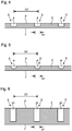
- FIG. 1 depicts an example configuration for the membrane 2.
- the membrane 2 is attached to a support structure 8,10.
- the combination of the membrane 2 and support structure 8,10 may be referred to as a membrane assembly 36.
- the membrane assembly 36 may be formed by manufacturing a plurality of membrane assemblies using a single integral membrane 2 (e.g. a wafer) and cutting out the membrane assembly 36 from the plurality of membrane assemblies.
- the plurality of membrane assemblies may remain connected together with the apparatus 1 being configured to interact with just one of the membrane assemblies.
- other instances of the apparatus 1 may be provided to interact with other ones of the membrane assemblies.
- the membrane assembly 36 may comprise the whole of a wafer forming the membrane 2.
- a voltage applicator for applying a voltage across the membrane 2, including in target regions 5.
- the voltage is applied via the ionic solution 32,34 and the first and second surface area portions 6,7 of the membrane 2.
- the voltage applicator comprises a first electrode 28 and a second electrode 30.
- the first electrode 28 is configured to contact the ionic solution 32 in the first bath 38.
- the second electrode 30 is configured to contact the ionic solution 34 in the second bath 40.
- the voltage applicator comprises a controller 26 for controlling the voltage applied by the voltage applicator.
- the apparatus 1 is configured such that a voltage applied via the first and second electrodes 28,30 can cause formation of a single aperture 20 in each of the target regions 5.
- the target regions 5 are spaced apart from each sufficiently that the reduction in resistance that occurs when dielectric breakdown is initiated in one target region 5 does not prevent dielectric breakdown from being initiated in a neighbouring target region 5. This is important because although the voltage is applied simultaneously to all of the target regions 5, the exact moment when dielectric breakdown begins may vary significantly between different target regions. The reduction in resistance will tend to reduce the magnitude of the electric field in the region of the target region 5.
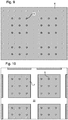
- Figures 7 and 8 are top and bottom plan views respectively of a portion of the membrane 2 of Figure 1 .
- the first surface area portion 6 ( Figure 7 ) consists of a single area without any holes.
- the second surface area portion 7 comprises a plurality of isolated regions which are separated from each other by the layer 8 of the support structure.
- the white areas shown correspond to a bottom surface 22 of layer 10 of the support structure.
- the isolated regions of the second surface area portion 7 are square with dimensions 15x15 microns.
- the shape of the isolated regions is determined by the particular process chosen for fabrication. KOH etch produces square shape etch pits but reactive ion etch could take any other shape, for example, circular shape (e.g. with diameter of 15 microns).
- the sequence of the first and second voltages is applied a plurality of times. This may be necessary to ensure that apertures 20 are initiated in all of the target regions 5.
- the sequence of first and second voltages may be applied repeatedly until it is detected that the current across the membrane 2 is stable. The inventors found that applying this approach to the arrangement shown in Figure 1 , for example, can be used reliably to produce plural apertures 20 having a uniform diameter of 15nm.
- the above described embodiments, and other embodiments, allow membranes 2 to be formed which comprise a plurality of apertures 20.
- the aperture diameter can be controlled by the thickness of the material in which the apertures are formed, for example by growing each aperture until its diameter is equal to or greater than a thickness of the membrane material separating the two baths in the region where the aperture is formed.
- Modern fabrication processes allow the membrane thickness to be controlled with very high precision (e.g. down to 1nm or less), thereby allowing accurate control of the aperture diameter. It is not essential for each aperture to be grown until its diameter is equal to or greater than a thickness of the membrane 2 in the region where the aperture is formed. In other embodiments, apertures are formed that are smaller than this.
- Relatively high voltages can be required to initiate the dielectric breakdown process. This is particularly the case where relatively large apertures (e.g. greater than about 30nm) need to be formed, because this requires a thicker membrane in the target regions and, consequently, a higher voltage for breakdown.
- the sudden reduction in resistance that occurs when the dielectric breakdown first occurs can lead to a large current flowing through the baths 32 and 34 and newly formed aperture 20.
- the large current could in principle oxidise or reduce a species present in the ionic solution in the baths and/or lead to damage to, or unpredictable behaviour of, the aperture 20 itself.
- an applied voltage of 20-30V is required to initiate dielectric breakdown.
- the current driven through the system after dielectric breakdown can completely destroy the aperture 20.
- the required aspect ratio of the fluidic resistor can be very large.
- a ⁇ 2nm diameter aperture 20 in a 10nm thick membrane 2 will require 20-30 ⁇ m long fluidic channel if the diameter is limited to 100nm.
- Increasing the resistivity of solution in the fluidic resistor can help reduce the aspect ratio requirement. Since there is no diffusion across the membrane 2 before dielectric breakdown, diluting the solution to increase the resistivity can proportionally reduce the required aspect ratio of the fluidic resistor if application of the voltage is stopped quickly after breakdown, before diffusion reaches the steady state.
- ⁇ cis and ⁇ trans are the bulk resistivity of solution in the cis and trans chamber respectively. According to this equation, a same 2nm diameter and 10nm thick pore only requires ⁇ 115nm diameter and 1 ⁇ m long fluidic resistor if we fill the fluidic resistor with a solution that is 1000 times more resistive.
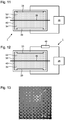
- Figures 14 and 15 show schematically a portion of a membrane 2 in which fluidic passages 24 having different aspect ratios have been formed, each of these fluidic passages 24 thereby having different fluidic resistances relative to each other.
- the left fluidic passage 24 in this particular example had a diameter of 50nm and the right a diameter of 100nm.
- the fluidic passages 24 were formed in a 300nm thick SiNx membrane 2.
- the thickness of the membrane 2 at the end of the fluidic passages 24 was 10nm. It was found that applying 10V across the membrane 2 caused a single aperture 20 to be formed in each of the two fluidic passages 24.
- Providing a fluidic passage 24 having a large enough aspect ratio to provide a functionally significant fluidic electrical resistance may require a thicker membrane 2 than is required in embodiments with shallower recesses 4 (e.g. as in Figures 4 and 5 ).
- a 300nm membrane 2 formed from SiNx was used, with fluidic passages 24 formed lithographically.
- the etch process needs to be stopped at the appropriate point to ensure the thickness of the membrane 2 at the end of the fluidic passages 24 is as required.
- small thicknesses e.g. 10nm
- the use of a membrane 2 formed from multiple layers of different compositions can be used more generally to achieve accurate thicknesses of target regions 5, recesses 4 and/or fluidic passages 24 of any form, due to different etching rates of the individual layers. Interfaces between layers of different compositions, which correspond to sudden changes or stopping of an etching process when the interfaces are reached, can be used to define any boundaries of structures formed in the membrane 2 (e.g. bottoms of recesses 4 or ends of fluidic passages 24).
- the membrane 2 comprises a first layer (e.g. the upper layer 2A in Figure 15 ) and a second layer (e.g.
- atomic layer deposition allows very uniform and precise thickness control at resolutions of the order of ⁇ 1 ⁇ .
- Materials which are inert to many reactive ion etch (RIE) processes can be applied using atomic layer deposition.
- the level of control provided by atomic layer deposition is higher than can be achieved typically using alternative film growth techniques.
- the length of the aperture which is dictated by the thickness of the layer or layers in which the aperture is formed (e.g. the lower layer 2B in Figure 15 ), can be controlled with high accuracy. More details about example configurations for the second layer (e.g. materials and sub-layers) are given below.
- fluidic passages 24 are provided using a porous layer which comprises pores that allow the ionic solution to pass from one side of the porous layer to the other side of the porous layer.
- the pores in this case are fluidic passages.
- This approach is a convenient way of providing fluidic passages 24 of high aspect ratio, due to the naturally narrow form adopted by pores in many porous materials.
- apertures 20 may be formed at the end of every pore of the porous layer that is traversed by the ionic solution. This may be desirable where the spatial distribution of the pores is suitable. However, in many cases it may be desired to form apertures 20 that are spaced apart differently (e.g. further apart), and/or are provided in different numbers (e.g.
- the porous layer may be provided in combination with a layer which comprises other fluidic passages 24 which define where the apertures 20 will be formed.
- the porous layer may provide a plurality of fluidic passages 24 which are fluidically in parallel with each other but in series with a further fluidic passage 24 provided in a separate layer which defines where the aperture 20 will be formed.
- the fluidic passage 24 in the separate layer will therefore have an opening which provides access to a plurality of the fluidic passages 24 provided by the porous layer.
- the porous layer may comprise a layer of anodized aluminium oxide (AAO).
- AAO can be formed with very high aspect ratio pores (e.g. greater than 1000:1), spaced apart in a lattice with a lattice constant of several hundred nanometres. The pore diameter and lattice constant can be tuned by forming the AAO on a suitably pre-patterned surface.
- fluidic passages 24 acting as current limiting resistors may be formed as channels within a layer of PDMS, oxide, and/or nitride.
- Embodiments have been described which allow membranes 2 to be formed which comprise a plurality of target regions 5 in each of which an aperture 20 is formed.
- Each target region 5 comprises a recess 4 or a fluidic passage 24 defining where the aperture 20 will be formed.
- Each aperture 20 is located within a different one of the target regions 5 and has a diameter determined by the resistance of any limiting resistor, the voltage regime applied and/or the thickness of the target region 5.
- the diameter may be equal to or greater than a minimum thickness of the membrane material separating the first and second baths where thickness is used as a primary means to control the diameter. Alternatively the diameter can be made smaller than the thickness of the membrane material.
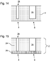
- Figures 16-19 depict steps in an example method of manufacturing a membrane assembly 36 in which atomic layer deposition is used to form a membrane 2.
- the membrane 2 is suitable for allowing formation of one or more apertures using dielectric breakdown according to any of the embodiments described herein.
- Figure 16 shows an arrangement which may be formed in the same way as the membrane assembly 36 described above with reference to Figure 1 , except that the arrangement of Figure 16 does not yet have any recesses 4 formed in a membrane.
- the upper covering layer 51 in Figure 16 may be formed in the same way as the membrane 2 of Figure 1 (e.g. from SiNx).
- the lower covering layer 52 of Figure 16 may be formed in the same way as layer 10 in Figure 1 (e.g. from SiNx).
- Atomic layer deposition is used to deposit an ALD layer 54 to provide the arrangement shown in Figure 17 .
- Atomic layer deposition which may be referred to as ALD, is a known technique for depositing thin films of material. The following is one example of a review paper on this topic: Steven M. George, "Atomic Layer Deposition: An Overview", Chem. Rev. 2010, 110, 111-131 .
- a fluidic passage 24 is formed in the upper covering layer 51, for example by lithography followed by a reactive ion etch.
- the fluidic passage 24 may be formed, for example, by etching through the upper covering layer 51 to the interface between the upper covering layer 51 and the ALD layer 54.
- the membrane assembly 36 shown in Figure 18 is thereby provided.
- the ALD layer 54 could be deposited at an earlier stage, for example prior to processing of a wafer to form the layer 8 (e.g. by KOH etching to selectively remove portions of the wafer to form the layer 8, which make the structure more fragile) and/or prior to growth of the upper covering layer 51 (e.g. SiNx).
- the ALD layer 54 may even be sandwiched between two layers forming all or part of the upper covering layer 51 (e.g. between two SiNx layers).
- Forming the ALD layer 54 earlier may desirably reduce the number of processing steps that need to be carried out while the membrane assembly is in a relatively fragile state (e.g. while thin membranes are present and/or after a wafer has been processed to form the layer 8).
- the membrane assemblies 36 shown in Figures 18 and 19 are examples in which a membrane 2 comprises a first layer (the upper covering layer 51 in Figures 18 and 19 ) and a second layer (the ALD layer 54 in Figures 18 and 19 ), and the second layer is formed by atomic layer deposition.
- the plurality of sub-layers 61,62 comprises a sequence of sub-layers 61,62 that repeats a plurality of times, each repeating sequence comprising at least a first sub-layer 61 and a second sub-layer 62 directly adjacent to the first sub-layer 61.
- the first sub-layers 61 have a different composition to the second sub-layers 62.
- each unit of the repeating sequence consists of a single first sub-layer 61 and a single second sub-layer 62 but this is not essential.
- each repeating unit may comprise more than two sub-layers (e.g. three sub-layers, four sub-layers, or more).
- all of the first sub-layers 61 have the same composition as each other and all of the second sub-layers 62 have the same composition as each other.
- a repeating sequence comprising four units, each consisting of a first sub-layer 61 and a second sub-layer 62 is shown for ease of depiction (with an additional first sub-layer 61 being provided so that the two outermost surfaces of the plurality of sub-layers have the same composition). In practice a larger number of sub-layers will normally be provided.
- each of the first and second sub-layers 61,62 is formed using four or fewer cycles of atomic layer deposition, for example one cycle, two cycles, three cycles, or four cycles.
- each of one or both of the first and second sub-layers 61,62 can be formed using more than four cycles of atomic layer deposition.
- Each of the first and second sub-layers 61,62 will typically have a thickness of the order of ⁇ 1 ⁇ per cycle of atomic layer deposition used to create them.
- the number of first and second sub-layers 61,62 (and any other sub-layers that are provided) is chosen to provide a desired overall thickness for the plurality of sub-layers.
- the thickness of the plurality of sub-layers 61,62 defines the length of any aperture formed through the plurality of sub-layers 61,62.
- the thickness of the plurality of sub-layers 61,62 is in the range of 2-6nm, optionally 2-4nm, optionally 2-3nm. In an embodiment, about 20-60 cycles of atomic layer deposition are used to form the plurality of sub-layers 61,62.
- the first sub-layers 61 are non-epitaxial with respect to the second sub-layers 62. Arranging for the first sub-layers 61 to be non-epitaxial with respect to the second sub-layers 62 reduces the formation of defects due to crystal growth within the sub-layers 61,62, preserving an amorphous film. Where the plurality of sub-layers comprises other sub-layers, it is preferably arranged that all sub-layers are non-epitaxial with respect to any directly adjacent sub-layers.
- the first sub-layers 61 and the second sub-layers 62 can be formed from a wide range of different materials.
- the first sub-layers 61 comprise HfO 2 and the second sub-layers 62 comprise Al 2 O 3 .
- HfO 2 has good dielectric properties. These two materials are compatible with atomic layer deposition and are non-epitaxial with respect to each other.
- the removal of the protective layer 63 will result in a repeating sequence of sub-layers 61,62 and an additional layer, such that the two outermost sub-layers are both first sub-layers 61 (as shown in Figures 20 and 21 ).
- An aperture is subsequently formed by dielectric breakdown through the freestanding membrane.
- one or more of the apertures 20 formed using the methods and apparatus discussed above, or according to other embodiments are used to sense a molecular entity by performing a measurement (e.g. an electrical measurement or an optical measurement) that is dependent on an interaction between the molecular entity and the aperture.
- a sensing apparatus is provided having a plurality of the apertures 20 thus formed and a measurement system configured to sense a molecular entity in each of the apertures 20 by performing a measurement that is dependent on an interaction between the molecular entity and the aperture 20.
- Sensing of molecular entities can provide the basis for identifying single molecules and molecular entities. There are a wide range of possible applications, such as sequencing of DNA or other nucleic acids; sensing of chemical or biological molecules for security and defence; detection of biological markers for diagnostics; ion channel screening for drug development; and label free analysis of interactions between biological molecules.
- the polynucleotide may be labelled with one of more of a fluorescent label, an optical label, a magnetic species or a chemical species, wherein detection of the species or label is indicative of the polynucleotide.
- Nucleic acid probes may be hybridised to the polynucleotide and resultant structure detected by translocation through an aperture of the array, such as disclosed in published application WO2007/041621 .
- the polynucleotide may be labelled with one or more acceptor labels, which interact with one or more donor labels attached to an aperture of the array, such as disclosed by published application WO2011/040996 .
- the polynucleotide may be any synthetic nucleic acid known in the art.
- the molecular entity may be an aptamer. The molecular entity is caused to translocate the aperture and the interactions between the molecular entity and the aperture measured.
- the solid state membrane may comprise either or both of organic and inorganic materials, including, but not limited to, microelectronic materials, whether electrically conducting, electrically semiconducting, or electrically insulating, including materials such as II-IV and III-V materials, oxides and nitrides, such as silicon nitride, Al 2 O 3 , and SiO 2 , Si, MoS 2 , solid state organic and inorganic polymers such as polyamide, plastics such as Teflon®, or elastomers such as two-component addition-cure silicone rubber, and glasses.
- a membrane may be formed from monatomic layers, such as graphene, or layers that are only a few atoms thick such as those disclosed in U.S. Patent No.
- a biological nanopore may be provided within a solid state aperture.
- a biological nanopore may be provided within a solid state aperture.
- the measurement may for example be electrical, optical or both.
- the electrical measurement may comprise measurement of ion flow through the apertures under a potential difference or concentration gradient. Electrical measurements may be made using standard single channel recording equipment as described in Stoddart D et al., Proc Natl Acad Sci, 12;106(19):7702-7 , Lieberman KR et al, J Am Chem Soc. 2010;132(50):17961-72 , and International Application WO-2000/28312 . Alternatively, electrical measurements may be made using a multi-channel system, for example as described in International Application WO-2009/077734 and International Application WO-2011/067559 . Optical measurements may be combined with electrical measurements ( Soni GV et al., Rev Sci Instrum. 2010 Jan;81(1):014301 ).
- the sensing apparatus may comprise a measurement system arranged as disclosed in any of WO-2008/102210 , WO-2009/07734 , WO-2010/122293 , WO-2011/067559 or WO2014/04443 .
- the sensing apparatus may comprise electrodes arranged on each side of the membrane in order to measure an ion current through an aperture under a potential difference.
- the electrodes may be connected to an electrical circuit which includes a control circuit arranged to supply a voltage to the electrodes and a measurement circuit. arranged to measure the ion flow.
- a common electrode may be provided to measure ion flow through the apertures between the common electrode and electrodes provided on the opposite side of the membrane.
- one or more polymer units may be present in the pore at any particular time and the measurement carried out may be dependent on a group of k polymer units, where k is an integer.
- a group of k polymer units where k is greater than one may be referred to as a k-mer.
- this might be thought of as the measurement system having a "blunt reader head" that is bigger than the polymer unit being measured.
- Determination of a sequence characteristic of k polymer units involving the measurement of k-mers may be carried out by methods disclosed by International Patent Applications PCT/GB2012/052343 and PCT/GB2013/050381 .
- determination of sequence information or molecular sequence classification may be carried out using an artificial neural network (ANN).
- ANN artificial neural network
- the voltage used is preferably in a range having a lower limit selected from -400 mV, -300 mV, -200 mV, -150 mV, -100 mV, -50 mV, -20mV and 0 mV and an upper limit independently selected from +10 mV, + 20 mV, +50 mV, +100 mV, +150 mV, +200 mV, +300 mV and +400 mV.
- the voltage used is more preferably in the range 100mV to 2V. It is possible to increase discrimination between different nucleotides by an aperture by using an increased applied potential.
- measurement of a conductance or resistance may be carried out.
- Alternative or additional measurements associated with movement of the molecular entity with respect to the aperture may be carried out, such as measurement of a tunnelling current across the aperture ( Ivanov AP et al., Nano Lett. 2011 Jan 12;11(1):279-85 ), or a field effect transistor (FET) device, such as disclosed by WO 2005/124888 , US8828138 , WO 2009/035647 , or Xie et al, Nat Nanotechnol. 2011 Dec 11; 7(2): 119-125 .
- the measurement device may be an FET nanopore device comprising source and drain electrodes to determine the presence or passage of a molecular entity in the apertures.
Landscapes
- Chemical & Material Sciences (AREA)
- Engineering & Computer Science (AREA)
- Chemical Kinetics & Catalysis (AREA)
- Life Sciences & Earth Sciences (AREA)
- Health & Medical Sciences (AREA)
- Organic Chemistry (AREA)
- Physics & Mathematics (AREA)
- Electrochemistry (AREA)
- Materials Engineering (AREA)
- Metallurgy (AREA)
- Biomedical Technology (AREA)
- Proteomics, Peptides & Aminoacids (AREA)
- Biophysics (AREA)
- Biochemistry (AREA)
- Molecular Biology (AREA)
- Immunology (AREA)
- General Health & Medical Sciences (AREA)
- Analytical Chemistry (AREA)
- Inorganic Chemistry (AREA)
- Manufacturing & Machinery (AREA)
- Optics & Photonics (AREA)
- Wood Science & Technology (AREA)
- Zoology (AREA)
- Food Science & Technology (AREA)
- Nanotechnology (AREA)
- General Physics & Mathematics (AREA)
- Urology & Nephrology (AREA)
- Pathology (AREA)
- Hematology (AREA)
- Medicinal Chemistry (AREA)
- Spectroscopy & Molecular Physics (AREA)
- Microbiology (AREA)
- Biotechnology (AREA)
- Bioinformatics & Cheminformatics (AREA)
- General Engineering & Computer Science (AREA)
- Genetics & Genomics (AREA)
- Physical Or Chemical Processes And Apparatus (AREA)
- Separation Using Semi-Permeable Membranes (AREA)
- Semiconductor Integrated Circuits (AREA)
- Fixed Capacitors And Capacitor Manufacturing Machines (AREA)
Claims (15)
- Procédé de formation d'une pluralité d'ouvertures (20) dans une membrane à l'état solide (2) au moyen d'un claquage diélectrique, dans lequel la membrane (2) comprend une première partie de superficie (6) sur un côté de la membrane (2) et une seconde partie de superficie (7) de l'autre côté de la membrane (2), et chacune d'une pluralité de régions cibles (5) comprend un évidement (4) ou un passage fluidique (24) dans la membrane (2) qui débouche dans la première ou la seconde partie de superficie (6, 7), le procédé comprenant :la mise en contact de toute la première partie de superficie (6) de la membrane (2) avec un premier bain (38) comprenant une solution ionique et toute la seconde partie de superficie (7) avec un second bain (40) comprenant une solution ionique ; etl'application d'une tension à travers la membrane (2) par l'intermédiaire des première et seconde électrodes (28, 30) en contact respectif avec les premier et second bains (38, 40) comprenant des solutions ioniques pour former une ouverture (20) au niveau de chacune d'une pluralité de régions cibles (5) dans la membrane (2), les première et seconde électrodes (28, 30) permettant d'appliquer une différence de potentiel à travers toutes les régions cibles (5) simultanément.
- Procédé selon la revendication 1, dans lequel une seule ouverture (20) est formée dans chacune des régions cibles (5).
- Procédé selon la revendication 2, dans lequel l'ouverture (20) dans chaque région cible (5) est agrandie jusqu'à ce qu'un diamètre de l'ouverture (20) soit égal ou supérieur à une épaisseur minimale de matériau de membrane séparant le premier bain (38) du second bain (40) dans la région cible (5).
- Procédé selon une quelconque revendication précédent, dans lequel la membrane (2) comprend une pluralité de couches et dans lequel une limite de chacun d'un ou de plusieurs des évidements (4) ou passages fluidiques (24) est située au niveau d'une interface entre deux des couches.
- Procédé selon la revendication 4, dans lequel :la membrane (2) comprend une première couche et une seconde couche ;chacun parmi les un ou plusieurs évidements (4) ou passages fluidiques (24) est formé en retirant une partie de la première couche jusqu'à l'interface entre la première couche et la seconde couche, de sorte que ladite limite est formée par une surface de la seconde couche ; etla seconde couche est formée par dépôt de couche atomique.
- Procédé selon une quelconque revendication précédente, dans lequel :la membrane (2) comprend une première couche et une seconde couche ; etla formation d'une ouverture (20) au niveau de chaque région cible de la pluralité de régions cibles (5) se produit par claquage diélectrique à travers au moins une partie de la seconde couche.
- Procédé selon la revendication 6, dans lequel la seconde couche est formée par dépôt de couche atomique.
- Procédé selon la revendication 7, dans lequel la seconde couche comprend une pluralité de sous-couches (61, 62), chaque sous-couche (61,62) étant formée par dépôt de couche atomique.
- Procédé selon la revendication 8, dans lequel la pluralité de sous-couches (61, 62) comprend une séquence de sous-couches qui se répète plusieurs fois, chaque séquence répétitive comprenant au moins une première sous-couche (61) et une seconde sous-couche (62) directement adjacente à la première sous-couche (61).
- Procédé selon la revendication 9, dans lequel les premières sous-couches (61) sont non épitaxiales par rapport aux secondes sous-couches (62).
- Procédé selon la revendication 10, dans lequel les premières sous-couches (61) comprennent HfO2 et les secondes sous-couches (62) comprennent Al2O3.
- Procédé selon l'une quelconque des revendications 9 à 11, dans lequel chaque sous-couche (61, 62) dans la séquence répétitive est formée à l'aide de quatre cycles ou moins de dépôt de couche atomique.
- Procédé selon l'une quelconque des revendications 9 à 12, dans lequel :la seconde couche est formée avec une couche de protection (63) sur l'un ou les deux côtés de la séquence répétitive de sous-couches (61, 62) ;la couche de protection (63) est retirée avant la formation de l'ouverture (20) dans chaque région cible (5) afin de former une membrane autoportante (2) comprenant la séquence répétitive de sous-couches (61, 62) dans chaque région cible (5) ; etl'ouverture (20) dans chaque région cible (5) est formée par claquage diélectrique à travers la membrane autoportante (2).
- Procédé selon une quelconque revendication précédente, dans lequel une ou plusieurs des régions cibles (5) comprennent un passage fluidique (24) et dans chacun d'un ou de plusieurs des passages fluidiques (24) une ouverture (20) est formée qui présente une résistance électrique fluidique inférieure à 10 fois la résistance électrique fluidique du passage fluidique (24).
- Procédé selon une quelconque revendication précédente, dans lequel des passages fluidiques (24) présentant différentes résistances électriques fluidiques sont prévus dans différentes régions cibles (5), et une pluralité correspondante d'ouvertures de tailles différentes (20) croissent en parallèle par l'intermédiaire de la tension appliquée à travers les première et secondes électrodes (28, 30).
Priority Applications (1)
| Application Number | Priority Date | Filing Date | Title |
|---|---|---|---|
| EP20184193.9A EP3741452A1 (fr) | 2015-05-20 | 2016-05-20 | Procédés et appareil pour la formation d'ouvertures dans une membrane à l'état solide au moyen d'un claquage diélectrique |
Applications Claiming Priority (2)
| Application Number | Priority Date | Filing Date | Title |
|---|---|---|---|
| GBGB1508669.7A GB201508669D0 (en) | 2015-05-20 | 2015-05-20 | Methods and apparatus for forming apertures in a solid state membrane using dielectric breakdown |
| PCT/US2016/033487 WO2016187519A1 (fr) | 2015-05-20 | 2016-05-20 | Procédés et appareil pour la formation d'ouvertures dans une membrane à l'état solide au moyen d'un claquage diélectrique |
Related Child Applications (2)
| Application Number | Title | Priority Date | Filing Date |
|---|---|---|---|
| EP20184193.9A Division EP3741452A1 (fr) | 2015-05-20 | 2016-05-20 | Procédés et appareil pour la formation d'ouvertures dans une membrane à l'état solide au moyen d'un claquage diélectrique |
| EP20184193.9A Division-Into EP3741452A1 (fr) | 2015-05-20 | 2016-05-20 | Procédés et appareil pour la formation d'ouvertures dans une membrane à l'état solide au moyen d'un claquage diélectrique |
Publications (2)
| Publication Number | Publication Date |
|---|---|
| EP3297750A1 EP3297750A1 (fr) | 2018-03-28 |
| EP3297750B1 true EP3297750B1 (fr) | 2021-04-07 |
Family
ID=53506080
Family Applications (2)
| Application Number | Title | Priority Date | Filing Date |
|---|---|---|---|
| EP20184193.9A Pending EP3741452A1 (fr) | 2015-05-20 | 2016-05-20 | Procédés et appareil pour la formation d'ouvertures dans une membrane à l'état solide au moyen d'un claquage diélectrique |
| EP16727070.1A Active EP3297750B1 (fr) | 2015-05-20 | 2016-05-20 | Procédés et appareil pour la formation d'ouvertures dans une membrane à l'état solide au moyen d'un claquage diélectrique |
Family Applications Before (1)
| Application Number | Title | Priority Date | Filing Date |
|---|---|---|---|
| EP20184193.9A Pending EP3741452A1 (fr) | 2015-05-20 | 2016-05-20 | Procédés et appareil pour la formation d'ouvertures dans une membrane à l'état solide au moyen d'un claquage diélectrique |
Country Status (7)
| Country | Link |
|---|---|
| US (2) | US10596523B2 (fr) |
| EP (2) | EP3741452A1 (fr) |
| JP (1) | JP6937986B2 (fr) |
| CN (2) | CN113274888B (fr) |
| DK (1) | DK3297750T3 (fr) |
| GB (1) | GB201508669D0 (fr) |
| WO (1) | WO2016187519A1 (fr) |
Families Citing this family (28)
| Publication number | Priority date | Publication date | Assignee | Title |
|---|---|---|---|---|
| GB201202519D0 (en) | 2012-02-13 | 2012-03-28 | Oxford Nanopore Tech Ltd | Apparatus for supporting an array of layers of amphiphilic molecules and method of forming an array of layers of amphiphilic molecules |
| US10794895B2 (en) | 2015-02-05 | 2020-10-06 | President And Fellows Of Harvard College | Nanopore sensor including fluidic passage |
| GB201508669D0 (en) | 2015-05-20 | 2015-07-01 | Oxford Nanopore Tech Ltd | Methods and apparatus for forming apertures in a solid state membrane using dielectric breakdown |
| GB201611770D0 (en) | 2016-07-06 | 2016-08-17 | Oxford Nanopore Tech | Microfluidic device |
| GB201612458D0 (en) | 2016-07-14 | 2016-08-31 | Howorka Stefan And Pugh Genevieve | Membrane spanning DNA nanopores for molecular transport |
| US10752496B2 (en) * | 2017-09-22 | 2020-08-25 | Applied Materials, Inc. | Pore formation in a substrate |
| GB2574048B (en) | 2018-05-24 | 2021-06-16 | Oxford Nanopore Tech Ltd | Nanopore sensor component with electrostatic discharge protection |
| GB201812615D0 (en) | 2018-08-02 | 2018-09-19 | Ucl Business Plc | Membrane bound nucleic acid nanopores |
| GB201814369D0 (en) | 2018-09-04 | 2018-10-17 | Oxford Nanopore Tech Ltd | Method for determining a polymersequence |
| US11454624B2 (en) | 2018-09-28 | 2022-09-27 | Ofer Wilner | Nanopore technologies |
| GB201819378D0 (en) | 2018-11-28 | 2019-01-09 | Oxford Nanopore Tech Ltd | Analysis of nanopore signal using a machine-learning technique |
| KR20210138594A (ko) | 2019-03-12 | 2021-11-19 | 옥스포드 나노포어 테크놀로지즈 피엘씨 | 나노포어 감지 디바이스 및 이를 작동하는 방법 및 형성하는 방법 |
| GB201907243D0 (en) | 2019-05-22 | 2019-07-03 | Oxford Nanopore Tech Ltd | Sensing interactions between molecular entities and nanapores |
| US20220054986A1 (en) * | 2020-07-17 | 2022-02-24 | Microcontinuum, Inc. | Filtration Films Having Dense Packing of Pores of Uniform Size and Distribution, and Tools and Methods for Their Formation |
| WO2022020461A1 (fr) | 2020-07-22 | 2022-01-27 | Oxford Nanopore Technologies Inc. | Formation de nanopores à l'état solide |
| WO2022211951A1 (fr) * | 2021-03-31 | 2022-10-06 | Illumina, Inc. | Dispositifs de capteurs à nanopores |
| CN113363140B (zh) * | 2021-06-02 | 2023-03-28 | 南方科技大学 | 生物掩膜版以及在衬底上图案化的方法 |
| GB202108821D0 (en) | 2021-06-18 | 2021-08-04 | Ucl Business Ltd | Nanomechanically actuated nucleic acid nanopore |
| GB202108820D0 (en) | 2021-06-18 | 2021-08-04 | Ucl Business Ltd | Nucleic acid nanopore with enhanced sensing functionality |
| WO2022263669A1 (fr) | 2021-06-18 | 2022-12-22 | Ucl Business Ltd | Nanopore d'acide nucléique à fonctionnalité de détection améliorée |
| DE112021007658T5 (de) * | 2021-08-18 | 2024-03-14 | Hitachi High-Tech Corporation | Vorrichtung zur analyse biologischer proben |
| WO2023094806A1 (fr) | 2021-11-29 | 2023-06-01 | Oxford Nanopore Technologies Plc | Analyse de signal de mesure de nanopore |
| GB202118908D0 (en) | 2021-12-23 | 2022-02-09 | Oxford Nanopore Tech Ltd | Method |
| GB202118906D0 (en) | 2021-12-23 | 2022-02-09 | Oxford Nanopore Tech Ltd | Method |
| CN114950589B (zh) * | 2022-05-27 | 2024-02-09 | 复旦大学 | 一种mct/aao异质超薄膜在光控双向可调控离子传输的应用 |
| GB202216162D0 (en) | 2022-10-31 | 2022-12-14 | Oxford Nanopore Tech Plc | Method |
| WO2024094966A1 (fr) | 2022-11-01 | 2024-05-10 | Oxford Nanopore Technologies Plc | Système d'analyse biochimique et procédé de commande d'un système d'analyse biochimique |
| GB202307486D0 (en) | 2023-05-18 | 2023-07-05 | Oxford Nanopore Tech Plc | Method |
Citations (6)
| Publication number | Priority date | Publication date | Assignee | Title |
|---|---|---|---|---|
| KR20120000520A (ko) | 2010-06-25 | 2012-01-02 | 서울대학교산학협력단 | 나노 포어 구조를 이용한 dna 분석용 장치, 분석 방법 및 pcr 정량 검출 장치 |
| US20120234679A1 (en) | 2009-09-18 | 2012-09-20 | President And Fellows Of Harvard College | Nanometric Material Having a Nanopore Enabling High-Sensitivity Molecular Detection and Analysis |
| WO2013167952A1 (fr) | 2012-05-07 | 2013-11-14 | The University Of Ottawa | Procédé pour l'ajustement de la taille de nanopores à l'état solide |
| US20140262820A1 (en) | 2013-03-15 | 2014-09-18 | President And Fellows Of Harvard College | Fabrication of Nanopores In Atomically-Thin Membranes By Ultra-Short Electrical Pulsing |
| WO2015152003A1 (fr) * | 2014-04-02 | 2015-10-08 | 株式会社日立ハイテクノロジーズ | Procédé de formation de trou et dispositif de mesure |
| EP3227228A2 (fr) | 2014-12-01 | 2017-10-11 | Cornell University | Substrats contenant des nanopores avec des éléments électroniques nanométriques alignés et procédés de fabrication et d'utilisation associés |
Family Cites Families (37)
| Publication number | Priority date | Publication date | Assignee | Title |
|---|---|---|---|---|
| US6267872B1 (en) | 1998-11-06 | 2001-07-31 | The Regents Of The University Of California | Miniature support for thin films containing single channels or nanopores and methods for using same |
| EP1192453B1 (fr) | 1999-06-22 | 2012-02-15 | President and Fellows of Harvard College | Evaluation a l'echelle atomique et moleculaire de biopolymeres |
| AU2002315497A1 (en) | 2001-06-27 | 2003-03-03 | President And Fellows Of Harvard College | Control of solid state dimensional features |
| WO2005124888A1 (fr) | 2004-06-08 | 2005-12-29 | President And Fellows Of Harvard College | Transistor a effet de champ dans un nanotube au carbone suspendu |
| US20080020499A1 (en) * | 2004-09-10 | 2008-01-24 | Dong-Wook Kim | Nanotube assembly including protective layer and method for making the same |
| JP2008540070A (ja) * | 2005-04-29 | 2008-11-20 | ユニバーシティー オブ ロチェスター | 超薄多孔質ナノスケール膜、その製造方法および使用 |
| US20070190542A1 (en) | 2005-10-03 | 2007-08-16 | Ling Xinsheng S | Hybridization assisted nanopore sequencing |
| US20080113833A1 (en) | 2006-11-15 | 2008-05-15 | Francisco Fernandez | Methods of playing soccer games |
| US20110121840A1 (en) | 2007-02-20 | 2011-05-26 | Gurdial Singh Sanghera | Lipid Bilayer Sensor System |
| US20110005918A1 (en) | 2007-04-04 | 2011-01-13 | Akeson Mark A | Compositions, devices, systems, and methods for using a nanopore |
| US9121843B2 (en) | 2007-05-08 | 2015-09-01 | Trustees Of Boston University | Chemical functionalization of solid-state nanopores and nanopore arrays and applications thereof |
| GB0713402D0 (en) | 2007-07-11 | 2007-08-22 | Cardiff & Vale Nhs Trust | A method of diagnosing a condition using a neural network |
| WO2009035647A1 (fr) | 2007-09-12 | 2009-03-19 | President And Fellows Of Harvard College | Capteur moléculaire haute résolution en feuille de carbone avec ouverture dans la couche de feuille de carbone |
| GB0724736D0 (en) | 2007-12-19 | 2008-01-30 | Oxford Nanolabs Ltd | Formation of layers of amphiphilic molecules |
| KR20110138286A (ko) | 2009-04-20 | 2011-12-26 | 옥스포드 나노포어 테크놀로지즈 리미티드 | 지질 이분자층 센서 어레이 |
| WO2011040996A1 (fr) | 2009-09-30 | 2011-04-07 | Quantapore, Inc. | Séquençage ultrarapide de polymères biologiques au moyen de nanopores marqués |
| EP2507387B1 (fr) | 2009-12-01 | 2017-01-25 | Oxford Nanopore Technologies Limited | Dispositif et procedee d'analyse biochimique |
| US8828138B2 (en) | 2010-05-17 | 2014-09-09 | International Business Machines Corporation | FET nanopore sensor |
| CN103154729B (zh) | 2010-06-08 | 2015-01-07 | 哈佛大学校长及研究员协会 | 具有由石墨烯支持的人工脂质膜的纳米孔装置 |
| KR101979038B1 (ko) | 2011-03-15 | 2019-05-15 | 프레지던트 앤드 펠로우즈 오브 하바드 칼리지 | 나노미터 고체 상태 재료에서의 나노포어의 제어된 제조법 |
| US8981995B2 (en) * | 2011-06-03 | 2015-03-17 | Microsoft Technology Licensing, Llc. | Low accuracy positional data by detecting improbable samples |
| US10761043B2 (en) | 2011-07-22 | 2020-09-01 | The Trustees Of The University Of Pennsylvania | Graphene-based nanopore and nanostructure devices and methods for macromolecular analysis |
| US10175195B2 (en) | 2011-07-27 | 2019-01-08 | The Board Of Trustees Of The University Of Illinois | Nanopore sensors for biomolecular characterization |
| US20160162634A1 (en) | 2011-09-23 | 2016-06-09 | Oxford Nanopore Technologies Limited | Analysis of a polymer comprising polymer units |
| CN104039979B (zh) | 2011-10-21 | 2016-08-24 | 牛津纳米孔技术公司 | 使用孔和Hel308解旋酶表征目标多核苷酸的酶方法 |
| EP2798083B1 (fr) | 2011-12-29 | 2017-08-09 | Oxford Nanopore Technologies Limited | Procédé de caractérisation d'un polynucléotide au moyen d'une hélicase xpd |
| KR102086182B1 (ko) | 2011-12-29 | 2020-03-06 | 옥스포드 나노포어 테크놀로지즈 리미티드 | 효소 방법 |
| AU2013221356B2 (en) | 2012-02-16 | 2018-10-18 | The Regents Of The University Of California | Nanopore sensor for enzyme-mediated protein translocation |
| CA2866587C (fr) | 2012-02-16 | 2022-07-26 | Oxford Nanopore Technologies Limited | Analyse de mesures d'un polymere |
| WO2013154999A2 (fr) * | 2012-04-09 | 2013-10-17 | The Trustees Of Columbia University In The City Of New York | Procédé de préparation de nanopore, et utilisations de celui-ci |
| WO2013153359A1 (fr) | 2012-04-10 | 2013-10-17 | Oxford Nanopore Technologies Limited | Pores formés de lysenine mutante |
| US20140006308A1 (en) | 2012-06-28 | 2014-01-02 | Google Inc. | Portion-by-portion feedback for electronic books |
| WO2014105246A2 (fr) * | 2012-10-05 | 2014-07-03 | Massachusetts Institute Of Technology | Système de tri nano-fluidique pour la synthèse de gène et produits de réaction de pcr |
| GB201313121D0 (en) | 2013-07-23 | 2013-09-04 | Oxford Nanopore Tech Ltd | Array of volumes of polar medium |
| WO2016034591A2 (fr) | 2014-09-01 | 2016-03-10 | Vib Vzw | Pores mutants |
| WO2016049698A1 (fr) * | 2014-10-01 | 2016-04-07 | University Of Tasmania | Dispositif d'extraction et de concentration |
| GB201508669D0 (en) | 2015-05-20 | 2015-07-01 | Oxford Nanopore Tech Ltd | Methods and apparatus for forming apertures in a solid state membrane using dielectric breakdown |
-
2015
- 2015-05-20 GB GBGB1508669.7A patent/GB201508669D0/en not_active Ceased
-
2016
- 2016-05-20 CN CN202011124835.XA patent/CN113274888B/zh active Active
- 2016-05-20 CN CN201680028909.5A patent/CN107810048B/zh active Active
- 2016-05-20 WO PCT/US2016/033487 patent/WO2016187519A1/fr active Application Filing
- 2016-05-20 EP EP20184193.9A patent/EP3741452A1/fr active Pending
- 2016-05-20 EP EP16727070.1A patent/EP3297750B1/fr active Active
- 2016-05-20 DK DK16727070.1T patent/DK3297750T3/da active
- 2016-05-20 US US15/575,798 patent/US10596523B2/en active Active
- 2016-05-20 JP JP2018512832A patent/JP6937986B2/ja active Active
-
2020
- 2020-02-12 US US16/788,733 patent/US11986775B2/en active Active
Patent Citations (8)
| Publication number | Priority date | Publication date | Assignee | Title |
|---|---|---|---|---|
| US20120234679A1 (en) | 2009-09-18 | 2012-09-20 | President And Fellows Of Harvard College | Nanometric Material Having a Nanopore Enabling High-Sensitivity Molecular Detection and Analysis |
| KR20120000520A (ko) | 2010-06-25 | 2012-01-02 | 서울대학교산학협력단 | 나노 포어 구조를 이용한 dna 분석용 장치, 분석 방법 및 pcr 정량 검출 장치 |
| WO2013167952A1 (fr) | 2012-05-07 | 2013-11-14 | The University Of Ottawa | Procédé pour l'ajustement de la taille de nanopores à l'état solide |
| WO2013167955A1 (fr) | 2012-05-07 | 2013-11-14 | The University Of Ottawa | Fabrication de nanopores à l'aide de champs électriques élevés |
| US20140262820A1 (en) | 2013-03-15 | 2014-09-18 | President And Fellows Of Harvard College | Fabrication of Nanopores In Atomically-Thin Membranes By Ultra-Short Electrical Pulsing |
| WO2015152003A1 (fr) * | 2014-04-02 | 2015-10-08 | 株式会社日立ハイテクノロジーズ | Procédé de formation de trou et dispositif de mesure |
| JP2015197385A (ja) * | 2014-04-02 | 2015-11-09 | 株式会社日立ハイテクノロジーズ | 孔形成方法及び測定装置 |
| EP3227228A2 (fr) | 2014-12-01 | 2017-10-11 | Cornell University | Substrats contenant des nanopores avec des éléments électroniques nanométriques alignés et procédés de fabrication et d'utilisation associés |
Non-Patent Citations (10)
| Title |
|---|
| ERIC BEAMISH ET AL.: "Paper; Precise control of the size and noise of solid-state nanopores using high electric fields", NANOTECHNOLOGY, IOP, vol. 23, no. 40, 14 September 2012 (2012-09-14), BRISTOL, GB, XP020230108, ISSN: 0957-4484 |
| HAROLD KWOK ET AL.: "Long Passage Times of Short ssDNA Molecules through Metallized Nanopores Fabricated by Controlled Breakdown", ADVANCED FUNCTIONAL MATERIALS, vol. 24, no. 48, 13 December 2014 (2014-12-13), pages 7745 - 7753, XP055289670 |
| ITARU YANAGI ET AL: "Fabricating nanopores with diameters of sub-1 nm to 3 nm using multilevel pulse-voltage injection", SCIENTIFIC REPORTS, vol. 4, XP055200768, DOI: 10.1038/srep05000 |
| JIWOOK SHIM ET AL.: "Electron beam induced local crystallization of Hf02 nanopores for biosensing applications", NANOSCALE, vol. 5, no. 22, 1 January 2013 (2013-01-01), XP055312732, ISSN: 2040-3364 |
| JOSEPH LARKIN ET AL: "Slow DNA Transport through Nanopores in Hafnium Oxide Membranes", ACS NANO, AMERICAN CHEMICAL SOCIETY, US, vol. 7, no. 11, 26 November 2013 (2013-11-26), US , pages 10121 - 10128, XP055312731, ISSN: 1936-0851, DOI: 10.1021/nn404326f |
| KAROW JULIA: "Oxford Nanopore Presents Details on New High-throughput Sequencer, Improvements to MinIon", GENOMEWEB, 16 September 2014 (2014-09-16), pages 1 - 3, XP055879207 |
| KUAN AARON T ET AL: "Electrical pulse fabrication of graphene nanopores in electrolyte solution", APPLIED PHYSICS LETTERS, AMERICAN INSTITUTE OF PHYSICS, 2 HUNTINGTON QUADRANGLE, MELVILLE, NY 11747, vol. 106, no. 20, 18 May 2015 (2015-05-18), 2 Huntington Quadrangle, Melville, NY 11747, pages 1 - 6, XP012202668, ISSN: 0003-6951, DOI: 10.1063/1.4921620 |
| KYLE BRIGGS ET AL.: "Automated Fabrication of 2-nm Solid- State Nanopores for Nucleic Acid Analysis", SMALL, vol. 10, no. 10, 2 March 2014 (2014-03-02), pages 2077 - 2086, XP055312908 |
| KYLE BRIGGS ET AL: "Kinetics of nanopore fabrication during controlled breakdown of dielectric membranes in solution", NANOTECHNOLOGY, INSTITUTE OF PHYSICS PUBLISHING, BRISTOL, GB, vol. 26, no. 8, 4 February 2015 (2015-02-04), Bristol, GB, pages 084004, XP020279049, ISSN: 0957-4484, DOI: 10.1088/0957-4484/26/8/084004 |
| RADIN TAHVILDARI ET AL: "Integrating nanopore sensors within microfluidic channel arrays using controlled breakdown", LAB ON A CHIP, ROYAL SOCIETY OF CHEMISTRY, UK, vol. 15, no. 6, 1 January 2015 (2015-01-01), UK , pages 1407 - 1411, XP055289676, ISSN: 1473-0197, DOI: 10.1039/C4LC01366B |
Also Published As
| Publication number | Publication date |
|---|---|
| CN107810048B (zh) | 2020-11-10 |
| US20200179880A1 (en) | 2020-06-11 |
| US10596523B2 (en) | 2020-03-24 |
| EP3741452A1 (fr) | 2020-11-25 |
| CN113274888B (zh) | 2023-05-16 |
| CN107810048A (zh) | 2018-03-16 |
| US11986775B2 (en) | 2024-05-21 |
| JP6937986B2 (ja) | 2021-09-22 |
| EP3297750A1 (fr) | 2018-03-28 |
| DK3297750T3 (da) | 2021-06-14 |
| GB201508669D0 (en) | 2015-07-01 |
| JP2018527176A (ja) | 2018-09-20 |
| US20180141007A1 (en) | 2018-05-24 |
| WO2016187519A1 (fr) | 2016-11-24 |
| CN113274888A (zh) | 2021-08-20 |
Similar Documents
| Publication | Publication Date | Title |
|---|---|---|
| US11986775B2 (en) | Methods and apparatus for forming apertures in a solid state membrane using dielectric breakdown | |
| JP5562325B2 (ja) | 少なくとも1つのナノポアまたはマイクロポアを有するダイヤモンドフィルムを含む伝導度センサーデバイス | |
| EP2534284B1 (fr) | Systèmes et procédés permettant de manipuler une molécule dans un nanopore | |
| EP3196645B1 (fr) | Membrane nue de graphène comprenant un nanopore permettant la détection et l'analyse moléculaires à haute sensibilité | |
| EP2383776B1 (fr) | Dispositif de nanopore à corps solide pour l'évaluation de biopolymères | |
| US20080218184A1 (en) | Nanopore platforms for ion channel recordings and single molecule detection and analysis | |
| US20110192723A1 (en) | Systems and methods for manipulating a molecule in a nanopore | |
| AU2020294228B2 (en) | Apparatus and methods for controlling insertion of a membrane channel into a membrane | |
| EP3227228A2 (fr) | Substrats contenant des nanopores avec des éléments électroniques nanométriques alignés et procédés de fabrication et d'utilisation associés | |
| EP3700670B1 (fr) | Retrait et réinsertion de nanopores de protéine dans une membrane à l'aide d'un déséquilibre osmotique | |
| WO2016122797A1 (fr) | Structure de capacité bicouche réglable pour dispositifs biomédicaux | |
| EP2473849B1 (fr) | Puce de nitrure de silicium nanoporeuse pour l'analyse de profils d'expression génique | |
| EP3344993B1 (fr) | Cellule à nanopore à petite ouverture et grande électrode | |
| US20190094179A1 (en) | Method for simple fluidic addressing of a nanopore | |
| CN113164954B (zh) | 感测系统和操作方法 | |
| US20230266268A1 (en) | Solid state nanopore formation | |
| CN115485553A (zh) | 用于使用捕获的电荷形成双层以及以纳米孔阵列插入孔的系统和方法 | |
| CN109680052B (zh) | 纳米孔薄膜、基因测序装置及纳米孔薄膜的制备方法 | |
| US20200393407A1 (en) | Cross-gap-nanopore heterostructure device and method for identifying chemical substance |
Legal Events
| Date | Code | Title | Description |
|---|---|---|---|
| STAA | Information on the status of an ep patent application or granted ep patent |
Free format text: STATUS: THE INTERNATIONAL PUBLICATION HAS BEEN MADE |
|
| PUAI | Public reference made under article 153(3) epc to a published international application that has entered the european phase |
Free format text: ORIGINAL CODE: 0009012 |
|
| STAA | Information on the status of an ep patent application or granted ep patent |
Free format text: STATUS: REQUEST FOR EXAMINATION WAS MADE |
|
| 17P | Request for examination filed |
Effective date: 20171114 |
|
| AK | Designated contracting states |
Kind code of ref document: A1 Designated state(s): AL AT BE BG CH CY CZ DE DK EE ES FI FR GB GR HR HU IE IS IT LI LT LU LV MC MK MT NL NO PL PT RO RS SE SI SK SM TR |
|
| AX | Request for extension of the european patent |
Extension state: BA ME |
|
| DAV | Request for validation of the european patent (deleted) | ||
| DAX | Request for extension of the european patent (deleted) | ||
| REG | Reference to a national code |
Ref country code: DE Ref legal event code: R079 Ref document number: 602016055622 Country of ref document: DE Free format text: PREVIOUS MAIN CLASS: B01D0067000000 Ipc: C25F0003020000 |
|
| GRAP | Despatch of communication of intention to grant a patent |
Free format text: ORIGINAL CODE: EPIDOSNIGR1 |
|
| STAA | Information on the status of an ep patent application or granted ep patent |
Free format text: STATUS: GRANT OF PATENT IS INTENDED |
|
| RIC1 | Information provided on ipc code assigned before grant |
Ipc: B01D 69/06 20060101ALI20200221BHEP Ipc: B01D 69/02 20060101ALI20200221BHEP Ipc: C25F 3/02 20060101AFI20200221BHEP Ipc: G01N 33/487 20060101ALI20200221BHEP Ipc: C25F 3/14 20060101ALI20200221BHEP Ipc: C25F 7/00 20060101ALI20200221BHEP Ipc: B01D 67/00 20060101ALI20200221BHEP Ipc: B82Y 40/00 20110101ALI20200221BHEP |
|
| INTG | Intention to grant announced |
Effective date: 20200330 |
|
| GRAS | Grant fee paid |
Free format text: ORIGINAL CODE: EPIDOSNIGR3 |
|
| STAA | Information on the status of an ep patent application or granted ep patent |
Free format text: STATUS: GRANT OF PATENT IS INTENDED |
|
| GRAA | (expected) grant |
Free format text: ORIGINAL CODE: 0009210 |
|
| STAA | Information on the status of an ep patent application or granted ep patent |
Free format text: STATUS: THE PATENT HAS BEEN GRANTED |
|
| AK | Designated contracting states |
Kind code of ref document: B1 Designated state(s): AL AT BE BG CH CY CZ DE DK EE ES FI FR GB GR HR HU IE IS IT LI LT LU LV MC MK MT NL NO PL PT RO RS SE SI SK SM TR |
|
| REG | Reference to a national code |
Ref country code: GB Ref legal event code: FG4D |
|
| RAP3 | Party data changed (applicant data changed or rights of an application transferred) |
Owner name: OXFORD NANOPORE TECHNOLOGIES INC. |
|
| REG | Reference to a national code |
Ref country code: AT Ref legal event code: REF Ref document number: 1379800 Country of ref document: AT Kind code of ref document: T Effective date: 20210415 Ref country code: CH Ref legal event code: EP |
|
| REG | Reference to a national code |
Ref country code: DE Ref legal event code: R096 Ref document number: 602016055622 Country of ref document: DE |
|
| REG | Reference to a national code |
Ref country code: IE Ref legal event code: FG4D |
|
| REG | Reference to a national code |
Ref country code: DK Ref legal event code: T3 Effective date: 20210607 |
|
| RAP2 | Party data changed (patent owner data changed or rights of a patent transferred) |
Owner name: OXFORD NANOPORE TECHNOLOGIES LTD. |
|
| REG | Reference to a national code |
Ref country code: NL Ref legal event code: FP |
|
| REG | Reference to a national code |
Ref country code: SE Ref legal event code: TRGR |
|
| REG | Reference to a national code |
Ref country code: LT Ref legal event code: MG9D |
|
| REG | Reference to a national code |
Ref country code: NL Ref legal event code: PD Owner name: OXFORD NANOPORE TECHNOLOGIES LTD.; GB Free format text: DETAILS ASSIGNMENT: CHANGE OF OWNER(S), ASSIGNMENT; FORMER OWNER NAME: OXFORD NANOPORE TECHNOLOGIES INC. Effective date: 20210628 |
|
| REG | Reference to a national code |
Ref country code: AT Ref legal event code: MK05 Ref document number: 1379800 Country of ref document: AT Kind code of ref document: T Effective date: 20210407 |
|
| REG | Reference to a national code |
Ref country code: NO Ref legal event code: T2 Effective date: 20210407 |
|
| REG | Reference to a national code |
Ref country code: BE Ref legal event code: PD Owner name: OXFORD NANOPORE TECHNOLOGIES LTD.; GB Free format text: DETAILS ASSIGNMENT: CHANGE OF OWNER(S), ASSIGNMENT Effective date: 20210525 |
|
| PG25 | Lapsed in a contracting state [announced via postgrant information from national office to epo] |
Ref country code: LT Free format text: LAPSE BECAUSE OF FAILURE TO SUBMIT A TRANSLATION OF THE DESCRIPTION OR TO PAY THE FEE WITHIN THE PRESCRIBED TIME-LIMIT Effective date: 20210407 Ref country code: FI Free format text: LAPSE BECAUSE OF FAILURE TO SUBMIT A TRANSLATION OF THE DESCRIPTION OR TO PAY THE FEE WITHIN THE PRESCRIBED TIME-LIMIT Effective date: 20210407 Ref country code: HR Free format text: LAPSE BECAUSE OF FAILURE TO SUBMIT A TRANSLATION OF THE DESCRIPTION OR TO PAY THE FEE WITHIN THE PRESCRIBED TIME-LIMIT Effective date: 20210407 Ref country code: BG Free format text: LAPSE BECAUSE OF FAILURE TO SUBMIT A TRANSLATION OF THE DESCRIPTION OR TO PAY THE FEE WITHIN THE PRESCRIBED TIME-LIMIT Effective date: 20210707 Ref country code: AT Free format text: LAPSE BECAUSE OF FAILURE TO SUBMIT A TRANSLATION OF THE DESCRIPTION OR TO PAY THE FEE WITHIN THE PRESCRIBED TIME-LIMIT Effective date: 20210407 |
|
| PG25 | Lapsed in a contracting state [announced via postgrant information from national office to epo] |
Ref country code: LV Free format text: LAPSE BECAUSE OF FAILURE TO SUBMIT A TRANSLATION OF THE DESCRIPTION OR TO PAY THE FEE WITHIN THE PRESCRIBED TIME-LIMIT Effective date: 20210407 Ref country code: IS Free format text: LAPSE BECAUSE OF FAILURE TO SUBMIT A TRANSLATION OF THE DESCRIPTION OR TO PAY THE FEE WITHIN THE PRESCRIBED TIME-LIMIT Effective date: 20210807 Ref country code: GR Free format text: LAPSE BECAUSE OF FAILURE TO SUBMIT A TRANSLATION OF THE DESCRIPTION OR TO PAY THE FEE WITHIN THE PRESCRIBED TIME-LIMIT Effective date: 20210708 Ref country code: PL Free format text: LAPSE BECAUSE OF FAILURE TO SUBMIT A TRANSLATION OF THE DESCRIPTION OR TO PAY THE FEE WITHIN THE PRESCRIBED TIME-LIMIT Effective date: 20210407 Ref country code: PT Free format text: LAPSE BECAUSE OF FAILURE TO SUBMIT A TRANSLATION OF THE DESCRIPTION OR TO PAY THE FEE WITHIN THE PRESCRIBED TIME-LIMIT Effective date: 20210809 |
|
| REG | Reference to a national code |
Ref country code: DE Ref legal event code: R026 Ref document number: 602016055622 Country of ref document: DE |
|
| PLBI | Opposition filed |
Free format text: ORIGINAL CODE: 0009260 |
|
| PLAX | Notice of opposition and request to file observation + time limit sent |
Free format text: ORIGINAL CODE: EPIDOSNOBS2 |
|
| PG25 | Lapsed in a contracting state [announced via postgrant information from national office to epo] |
Ref country code: CZ Free format text: LAPSE BECAUSE OF FAILURE TO SUBMIT A TRANSLATION OF THE DESCRIPTION OR TO PAY THE FEE WITHIN THE PRESCRIBED TIME-LIMIT Effective date: 20210407 Ref country code: EE Free format text: LAPSE BECAUSE OF FAILURE TO SUBMIT A TRANSLATION OF THE DESCRIPTION OR TO PAY THE FEE WITHIN THE PRESCRIBED TIME-LIMIT Effective date: 20210407 Ref country code: SK Free format text: LAPSE BECAUSE OF FAILURE TO SUBMIT A TRANSLATION OF THE DESCRIPTION OR TO PAY THE FEE WITHIN THE PRESCRIBED TIME-LIMIT Effective date: 20210407 Ref country code: SM Free format text: LAPSE BECAUSE OF FAILURE TO SUBMIT A TRANSLATION OF THE DESCRIPTION OR TO PAY THE FEE WITHIN THE PRESCRIBED TIME-LIMIT Effective date: 20210407 Ref country code: MC Free format text: LAPSE BECAUSE OF FAILURE TO SUBMIT A TRANSLATION OF THE DESCRIPTION OR TO PAY THE FEE WITHIN THE PRESCRIBED TIME-LIMIT Effective date: 20210407 Ref country code: LU Free format text: LAPSE BECAUSE OF NON-PAYMENT OF DUE FEES Effective date: 20210520 Ref country code: RO Free format text: LAPSE BECAUSE OF FAILURE TO SUBMIT A TRANSLATION OF THE DESCRIPTION OR TO PAY THE FEE WITHIN THE PRESCRIBED TIME-LIMIT Effective date: 20210407 Ref country code: ES Free format text: LAPSE BECAUSE OF FAILURE TO SUBMIT A TRANSLATION OF THE DESCRIPTION OR TO PAY THE FEE WITHIN THE PRESCRIBED TIME-LIMIT Effective date: 20210407 |
|
| 26 | Opposition filed |
Opponent name: MAIWALD PATENTANWALTS- UND RECHTSANWALTSGESELLSCHAFT MBH Effective date: 20211223 |
|
| REG | Reference to a national code |
Ref country code: BE Ref legal event code: PD Owner name: OXFORD NANOPORE TECHNOLOGIES LTD.; GB Free format text: DETAILS ASSIGNMENT: CHANGE OF OWNER(S), ASSIGNMENT; FORMER OWNER NAME: OXFORD NANOPORE TECHNOLOGIES INC. Effective date: 20211230 |
|
| PLBB | Reply of patent proprietor to notice(s) of opposition received |
Free format text: ORIGINAL CODE: EPIDOSNOBS3 |
|
| PG25 | Lapsed in a contracting state [announced via postgrant information from national office to epo] |
Ref country code: IS Free format text: LAPSE BECAUSE OF FAILURE TO SUBMIT A TRANSLATION OF THE DESCRIPTION OR TO PAY THE FEE WITHIN THE PRESCRIBED TIME-LIMIT Effective date: 20210807 Ref country code: AL Free format text: LAPSE BECAUSE OF FAILURE TO SUBMIT A TRANSLATION OF THE DESCRIPTION OR TO PAY THE FEE WITHIN THE PRESCRIBED TIME-LIMIT Effective date: 20210407 |
|
| PG25 | Lapsed in a contracting state [announced via postgrant information from national office to epo] |
Ref country code: IT Free format text: LAPSE BECAUSE OF FAILURE TO SUBMIT A TRANSLATION OF THE DESCRIPTION OR TO PAY THE FEE WITHIN THE PRESCRIBED TIME-LIMIT Effective date: 20210407 |
|
| PG25 | Lapsed in a contracting state [announced via postgrant information from national office to epo] |
Ref country code: RS Free format text: LAPSE BECAUSE OF FAILURE TO SUBMIT A TRANSLATION OF THE DESCRIPTION OR TO PAY THE FEE WITHIN THE PRESCRIBED TIME-LIMIT Effective date: 20210407 Ref country code: HU Free format text: LAPSE BECAUSE OF FAILURE TO SUBMIT A TRANSLATION OF THE DESCRIPTION OR TO PAY THE FEE WITHIN THE PRESCRIBED TIME-LIMIT; INVALID AB INITIO Effective date: 20160520 |
|
| P01 | Opt-out of the competence of the unified patent court (upc) registered |
Effective date: 20230505 |
|
| PG25 | Lapsed in a contracting state [announced via postgrant information from national office to epo] |
Ref country code: CY Free format text: LAPSE BECAUSE OF FAILURE TO SUBMIT A TRANSLATION OF THE DESCRIPTION OR TO PAY THE FEE WITHIN THE PRESCRIBED TIME-LIMIT Effective date: 20210407 |
|
| PGFP | Annual fee paid to national office [announced via postgrant information from national office to epo] |
Ref country code: NO Payment date: 20230530 Year of fee payment: 8 Ref country code: NL Payment date: 20230526 Year of fee payment: 8 Ref country code: IE Payment date: 20230529 Year of fee payment: 8 Ref country code: FR Payment date: 20230525 Year of fee payment: 8 Ref country code: DK Payment date: 20230530 Year of fee payment: 8 Ref country code: DE Payment date: 20230530 Year of fee payment: 8 Ref country code: CH Payment date: 20230610 Year of fee payment: 8 |
|
| PGFP | Annual fee paid to national office [announced via postgrant information from national office to epo] |
Ref country code: SE Payment date: 20230527 Year of fee payment: 8 |
|
| PGFP | Annual fee paid to national office [announced via postgrant information from national office to epo] |
Ref country code: BE Payment date: 20230529 Year of fee payment: 8 |
|
| PGFP | Annual fee paid to national office [announced via postgrant information from national office to epo] |
Ref country code: GB Payment date: 20230529 Year of fee payment: 8 |
|
| PG25 | Lapsed in a contracting state [announced via postgrant information from national office to epo] |
Ref country code: MK Free format text: LAPSE BECAUSE OF FAILURE TO SUBMIT A TRANSLATION OF THE DESCRIPTION OR TO PAY THE FEE WITHIN THE PRESCRIBED TIME-LIMIT Effective date: 20210407 |