EP3295231B1 - Optoelektronisches bauelement - Google Patents
Optoelektronisches bauelement Download PDFInfo
- Publication number
- EP3295231B1 EP3295231B1 EP16729761.3A EP16729761A EP3295231B1 EP 3295231 B1 EP3295231 B1 EP 3295231B1 EP 16729761 A EP16729761 A EP 16729761A EP 3295231 B1 EP3295231 B1 EP 3295231B1
- Authority
- EP
- European Patent Office
- Prior art keywords
- waveguide
- coupling element
- plane
- coupling
- optical radiation
- Prior art date
- Legal status (The legal status is an assumption and is not a legal conclusion. Google has not performed a legal analysis and makes no representation as to the accuracy of the status listed.)
- Active
Links
Images



Classifications
-
- G—PHYSICS
- G02—OPTICS
- G02B—OPTICAL ELEMENTS, SYSTEMS OR APPARATUS
- G02B6/00—Light guides; Structural details of arrangements comprising light guides and other optical elements, e.g. couplings
- G02B6/24—Coupling light guides
- G02B6/26—Optical coupling means
- G02B6/28—Optical coupling means having data bus means, i.e. plural waveguides interconnected and providing an inherently bidirectional system by mixing and splitting signals
- G02B6/2804—Optical coupling means having data bus means, i.e. plural waveguides interconnected and providing an inherently bidirectional system by mixing and splitting signals forming multipart couplers without wavelength selective elements, e.g. "T" couplers, star couplers
- G02B6/2852—Optical coupling means having data bus means, i.e. plural waveguides interconnected and providing an inherently bidirectional system by mixing and splitting signals forming multipart couplers without wavelength selective elements, e.g. "T" couplers, star couplers using tapping light guides arranged sidewardly, e.g. in a non-parallel relationship with respect to the bus light guides (light extraction or launching through cladding, with or without surface discontinuities, bent structures)
-
- G—PHYSICS
- G02—OPTICS
- G02B—OPTICAL ELEMENTS, SYSTEMS OR APPARATUS
- G02B6/00—Light guides; Structural details of arrangements comprising light guides and other optical elements, e.g. couplings
- G02B6/10—Light guides; Structural details of arrangements comprising light guides and other optical elements, e.g. couplings of the optical waveguide type
- G02B6/12—Light guides; Structural details of arrangements comprising light guides and other optical elements, e.g. couplings of the optical waveguide type of the integrated circuit kind
- G02B6/12004—Combinations of two or more optical elements
-
- G—PHYSICS
- G02—OPTICS
- G02B—OPTICAL ELEMENTS, SYSTEMS OR APPARATUS
- G02B6/00—Light guides; Structural details of arrangements comprising light guides and other optical elements, e.g. couplings
- G02B6/10—Light guides; Structural details of arrangements comprising light guides and other optical elements, e.g. couplings of the optical waveguide type
- G02B6/12—Light guides; Structural details of arrangements comprising light guides and other optical elements, e.g. couplings of the optical waveguide type of the integrated circuit kind
- G02B6/122—Basic optical elements, e.g. light-guiding paths
- G02B6/125—Bends, branchings or intersections
-
- G—PHYSICS
- G02—OPTICS
- G02B—OPTICAL ELEMENTS, SYSTEMS OR APPARATUS
- G02B6/00—Light guides; Structural details of arrangements comprising light guides and other optical elements, e.g. couplings
- G02B6/24—Coupling light guides
- G02B6/26—Optical coupling means
- G02B6/28—Optical coupling means having data bus means, i.e. plural waveguides interconnected and providing an inherently bidirectional system by mixing and splitting signals
- G02B6/293—Optical coupling means having data bus means, i.e. plural waveguides interconnected and providing an inherently bidirectional system by mixing and splitting signals with wavelength selective means
- G02B6/29331—Optical coupling means having data bus means, i.e. plural waveguides interconnected and providing an inherently bidirectional system by mixing and splitting signals with wavelength selective means operating by evanescent wave coupling
- G02B6/29335—Evanescent coupling to a resonator cavity, i.e. between a waveguide mode and a resonant mode of the cavity
- G02B6/29338—Loop resonators
- G02B6/29341—Loop resonators operating in a whispering gallery mode evanescently coupled to a light guide, e.g. sphere or disk or cylinder
-
- G—PHYSICS
- G02—OPTICS
- G02B—OPTICAL ELEMENTS, SYSTEMS OR APPARATUS
- G02B6/00—Light guides; Structural details of arrangements comprising light guides and other optical elements, e.g. couplings
- G02B6/24—Coupling light guides
- G02B6/26—Optical coupling means
- G02B6/30—Optical coupling means for use between fibre and thin-film device
-
- G—PHYSICS
- G02—OPTICS
- G02B—OPTICAL ELEMENTS, SYSTEMS OR APPARATUS
- G02B6/00—Light guides; Structural details of arrangements comprising light guides and other optical elements, e.g. couplings
- G02B6/24—Coupling light guides
- G02B6/42—Coupling light guides with opto-electronic elements
- G02B6/4201—Packages, e.g. shape, construction, internal or external details
- G02B6/4204—Packages, e.g. shape, construction, internal or external details the coupling comprising intermediate optical elements, e.g. lenses, holograms
- G02B6/4214—Packages, e.g. shape, construction, internal or external details the coupling comprising intermediate optical elements, e.g. lenses, holograms the intermediate optical element having redirecting reflective means, e.g. mirrors, prisms for deflecting the radiation from horizontal to down- or upward direction toward a device
Definitions
- the invention relates to an optoelectronic component having the features according to the preamble of patent claim 1 and to a method for operating optoelectronic components.
- OPTICS EXPRESS 1567 discloses an optoelectronic component with an optical waveguide integrated in one plane of the component, which can guide optical radiation in the plane of the component, and a coupling element which is connected to the waveguide and which is guided in the waveguide and fed by it into the coupling element Radiation--along a main coupling path--can couple out of the plane and/or optical radiation fed in at an angle into the plane of the waveguide--along the main coupling path--into the waveguide and thus into the plane of the component.
- the invention is based on the object of further improving an optoelectronic component of the type specified.
- the optoelectronic component has, in addition to the waveguide already mentioned—referred to below as the first waveguide—a second waveguide, which is arranged with its longitudinal axis at an angle to the plane in which the integrated optical waveguide is integrated and can guide radiation , and the coupling element is connected to the first and second waveguide and the optical radiation guided in the first waveguide and fed into the coupling element can be coupled - along the main coupling path - in the direction out of the plane and into the second waveguide and/or in optical radiation guided by the second waveguide and fed by it into the coupling element - along the main coupling path - can be coupled into the first waveguide and thus into the plane of the component, the integrated optical waveguide and the coupling element in a semiconductor chip of the component int and the optoelectronic component has a control unit which is connected to the detector and which, based on the detector signal, influences at least one operating variable of the optoelectronic component, namely the temperature of the semiconductor chip of
- An essential advantage of the component according to the invention can be seen in the fact that the radiation loss generated by the coupling element is evaluated according to the invention and used to control the component, namely to control the temperature of the semiconductor chip. Specifically, it is provided according to the invention to use a detector to measure the radiation loss of the coupling element and to influence the temperature of the semiconductor chip of the component using the detector signal. In other words, according to the invention, lost radiation, which remains unused in previously known components, is used in a targeted manner as a measured variable for controlling the temperature of the semiconductor chip.
- the optoelectronic component can also be made for the optoelectronic component to have a transmission element, in particular a transmission element connected to the first or second waveguide.
- the control unit is configured in such a way that, based on the detector signal, it influences the transmission power of the transmission element as the operating variable or one of the operating variables of the optoelectronic component.
- the opening cross-section normal of the in-coupling end face of the detector preferably lies parallel to the plane of the component in which the first waveguide is integrated and can guide its optical radiation.
- the component preferably has a semiconductor chip or consists of one.
- the plane in which the first waveguide can guide optical radiation is preferably a chip plane of the semiconductor chip, in particular a layer plane of a semiconductor layer of a layer stack of the semiconductor chip.
- the coupling element preferably couples optical radiation fed in at an angle into the plane of the first waveguide—along at least two main coupling paths—into the first waveguide and into at least one further waveguide, which lies in the same plane of the component as the first waveguide and can guide optical radiation there.
- the coupling efficiency of the coupling element is preferably less than one with respect to the at least two main coupling paths, and the coupling element preferably has an associated secondary coupling path for each main coupling path.
- the coupling element when optical radiation is incident at an angle into the plane of the waveguide, in particular when optical radiation is incident through the second waveguide, - i.e. when radiation is deflected along the at least two main coupling paths - along each of the secondary coupling paths emits optical leakage radiation which is proportional or at least approximately proportional to the radiation transmitted along the respective main coupling path, and the detector detects at least one of the leakage radiation, preferably all leakage radiation, entirely or at least in part.
- the coupling element decouples the optical radiation guided in the first and/or in one of the further waveguides and fed into the coupling element by it, preferably along the respective main coupling paths at an angle out of the plane of the waveguides and thereby, for example, into the second waveguide.
- the detector is a photodiode or includes one.
- a detector layer of the photodiode preferably lies in that plane in which the first waveguide is integrated and can guide radiation, and/or in a plane parallel thereto.
- the photodiode can be realized, for example, as a germanium, indium phosphide, gallium arsenide or indium gallium arsenide photodiode, for example in the form of a pin or pn diode.
- the coupling element preferably comprises a grating, a mirror and/or a photonic crystal structure.
- the integrated optical waveguide is straight in the area of the coupling element and has two straight waveguide sections that directly adjoin the coupling element; the rectilinear waveguide sections are preferably aligned—seen in the longitudinal direction of the waveguide or along the direction of propagation of the optical radiation—or lie in a straight line one behind the other.
- One of the two straight waveguide sections preferably forms the main coupling path or at least a section of the main coupling path.
- the other of the two straight waveguide sections preferably forms the secondary coupling path or at least a section of the secondary coupling path.
- the first waveguide and the at least one further waveguide are each straight in the area of the coupling element and are preferably at an angle of between 70 and 90 degrees to one another.
- the coupling element is for the wavelength, the wavelengths or the wavelength band of the optical radiation which is guided in the optoelectronic component or at least in the first waveguide, the second waveguide and/or the at least one further waveguide and which the coupling element couples or should couple , preferably wavelength-independent or at least approximately wavelength-independent.
- the term “approximately wavelength-independent” is understood here to mean that the coupling efficiency for the wavelengths or the wavelength band of the optical radiation fluctuates by less than 20% ( ⁇ 1 dB), preferably less than 5% ( ⁇ 0.2 dB).
- the invention also relates to a method with the features according to patent claim 15.
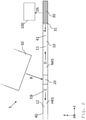
- the figure 1 1 shows an optoelectronic component 5 in a plan view, in which an integrated optical waveguide 10, a coupling element 20 and a detector 30 are integrated in a semiconductor chip 40 of the component 5.
- FIG. The reference symbols X, Y and Z designate the spatial coordinates of the component.
- the coupling element 20 also couples the integrated optical waveguide 10—hereinafter referred to as the first waveguide a second waveguide, which in the embodiment according to figure 1 is formed by an optical fiber 50.
- the optical fiber 50 is positioned with its longitudinal axis at an angle to the plane EB (cf. figure 2 ), in which the integrated optical waveguide 10, the coupling element 20 and the detector 30 are integrated in the semiconductor chip 40.
- the coupling element 20 divides the integrated optical waveguide 10 in the illustration according to FIG figure 1 into one in the figure 1 right waveguide section 11 and one in the figure 1 left waveguide section 12.
- the coupling element 20 is designed such that it mainly couples the left waveguide section 12 to the optical fiber 50 and forms a main coupling path HKS between the left waveguide section 12 and the optical fiber 50.
- the coupling element 20 can be formed, for example, by a 1D or 2D grating coupler or a deflection unit.
- the coupling efficiency of the coupling element 20 is very high with respect to the main coupling path HKS, i.e. between the left-hand waveguide section 12 and the optical fiber 50, but - due to diffraction, refraction, scattering and/or reflection - is less than one, so that the coupling element 20 Optical fiber 50 with the in the figure 1 right waveguide section 11 couples and between the right waveguide section 11 and the optical fiber 50 forms a secondary coupling path NKS.
- the detector 30 can be in the figure 1 recognize that a coupling face 31 of the detector 30 connected to the integrated optical waveguide 10 is aligned in such a way that the opening cross-section normal A of the coupling face 31 is parallel lies to the plane of the semiconductor chip 40 in which the integrated optical waveguide 10 and the coupling element 20 are integrated.
- the detector 30 can be realized, for example, as a germanium, indium phosphide, gallium arsenide or indium gallium arsenide photodiode or as a p- and n-doped semiconductor region as part of a pin or pn diode.
- a control unit 100 is connected to the detector 30 and evaluates a detector signal DS generated by the detector 30 and influences at least one operating variable of the optoelectronic component 5 using the detector signal DS.
- the functioning of the optoelectronic component 5 is to be explained below by way of example for the case in which the optical fiber 50 couples optical radiation B into the coupling element 20 . If optical radiation B is coupled in from the optical fiber 50, the coupling element 20 will couple the majority of the radiation B along the main coupling path HKS into the left-hand waveguide section 12; the coupled radiation is in the figure 1 marked with the reference C.
- a small part of the optical radiation B is - due to diffraction, refraction, scattering and/or reflection in the coupling element 20 - coupled via the secondary coupling path NKS as radiation loss D into the right waveguide section 11 and transmitted to the detector 30 via this.
- the detector 30 generates the detector signal DS, which reaches the control unit 100.
- the control unit 100 can determine which radiation power over the main coupling path HKS is coupled into the semiconductor chip 40, and adjust the optical component 5 accordingly.
- the control unit 100 can be designed in such a way that it controls a cooling and/or heating element of the component 5 based on the detector signal DS in order to keep the temperature of the optoelectronic component 5 in a desired temperature range.
- the left-hand waveguide section 12 and the right-hand waveguide section 11 are each straight in the region of the coupling element and form two straight-line waveguide sections which directly adjoin the coupling element 20 .
- the straight waveguide sections are aligned—seen in the longitudinal direction of the waveguide or along the direction of propagation of the optical radiation—or are located one behind the other, viewed in the longitudinal direction of the waveguide or along the direction of propagation of the optical radiation.
- the figure 2 shows the optoelectronic component 5 according to FIG figure 1 in cross section.
- the angular arrangement of the optical fiber 50 relative to the plane EB and thus to the optical waveguide 10, which is integrated in the plane EB of the semiconductor chip 40, can be seen.
- the integrated optical waveguide 10, the coupling element 20 and the detector 30 are integrated in one or more semiconductor layers 41, which belong to a semiconductor layer stack of the semiconductor chip 40, not shown in detail.
- the semiconductor chip 40 can be SOI (silicon on insulator) material, for example; in this case it acts
- the semiconductor layer 41 is preferably a silicon layer overlying a silicon dioxide layer.
- the figure 3 shows an embodiment of an optoelectronic component 5, which is essentially the first embodiment according to the figures 1 and 2 is equivalent to.
- the left waveguide section 12 of the optical waveguide 10 is connected to a transmission element 200 .
- the transmission element 200 can generate optical radiation B and couple it into the coupling element 20 .
- the coupling element 20 couples the optical radiation B coupled in along the main coupling path HKS out of the plane of the semiconductor layer 41 and thus out of the semiconductor chip 40 and couples it into the optical fiber 50 arranged at an angle to the semiconductor chip 40 .
- the radiation coupled out of the semiconductor chip 40 is in the figure 3 marked with the reference C.
- the coupling element 20 couples a small proportion of the optical radiation B into the right-hand waveguide section 11 - along the secondary coupling path NKS - as leakage radiation D and thus to the detector 30 transferred, which detects the radiation loss D metrologically.
- Detector 30 generates a detector signal DS that reaches control unit 100 .
- the control unit 100 evaluates the detector signal DS and uses the detector signal to influence, for example, at least one operating variable of the transmission element 200, for example the transmission power of the transmission element 200, and/or for example at least one heating element of the optoelectronic component 5 in order to keep the optoelectronic component 5, in particular the semiconductor chip 40, in a predetermined operating parameter range, for example in a predetermined temperature range.
- a control signal ST which the control unit 100 transmits to the transmission element 200 via a control line 101 .
- the figure 4 1 shows an exemplary embodiment of an optoelectronic component 5 in which a coupling element 20 integrated in a semiconductor chip 40 has or provides two main coupling paths HKS1 and HKS2 and two secondary coupling paths NKS1 and NKS2.
- the coupling element 20 couples an optical waveguide 10 integrated in the semiconductor chip 40—hereinafter referred to as the first waveguide—to a second waveguide located outside of the semiconductor chip 40, which is, for example, an optical fiber like the optical fiber 50 according to the Figures 1 to 3 can act; the second waveguide is in the figure 4 not shown further for reasons of clarity.
- the coupling element 20 couples the second waveguide to a further waveguide—referred to below as the third waveguide 300—which—just like the waveguide 10—is integrated in the semiconductor chip 40 and is preferably arranged in the same waveguide plane as the waveguide 10.
- the first waveguide 10 and the third waveguide 300 are preferably perpendicular to one another. For example, if optical radiation B is coupled into the coupling element 20 through the second waveguide by angled irradiation, then this is coupled into both the first waveguide 10 and the third waveguide 300 via the main coupling paths HKS1 and HKS2; the coupled radiation is in the figure 4 denoted by the references C and C2.
- the coupling element 20 couples leakage radiation D and D2 into the two waveguides 10 and 300 via the secondary coupling paths NKS1 and NKS2.
- the radiation leakage D and D2 arrives via the waveguides 10 and 300 at the in-coupling end faces 31 of a detector 30 which metrologically detects the radiation leakage D and D2 and generates a corresponding detector signal DS for a control unit 100 on the output side.
- the control unit 100 can use the detector signal to influence at least one operating variable of the optoelectronic component 5, as in connection with the Figures 1 to 3 has already been explained in detail above.
- the waveguide sections 501 and 502 of the waveguide 10 and the waveguide sections 511 and 512 of the waveguide 300 are each rectilinear in the area of the coupling element.
- the straight waveguide sections 501 and 502 or 511 and 512 are aligned in pairs, viewed in the longitudinal direction of the waveguide or along the direction of propagation of the optical radiation.
- FIG. 1 shows an exemplary embodiment of an optoelectronic component 5 that is equipped with a ring resonator 140.
- the lost radiation D coupled out of a coupling element 20 via a secondary coupling path NKS is coupled into a waveguide 150 via the ring resonator 140 and into a detector 30 via the waveguide 150 .
- a spectral filtering takes place through the transmission spectrum of the ring resonator 140, which can be adapted or set, for example, via the ring geometry. For example, specific spectral modulation sidebands of a modulated data signal can be selectively transmitted.
- the filtered radiation loss H reaches the detector 30.
- the detector 30 is connected to a control unit 100 which, based on the detector signal DS or based on the filtered radiation loss H, controls the optoelectronic component 5 or influences at least one operating variable of the optoelectronic component 5 .
- the figure 6 shows an embodiment of an optoelectronic component 5, in which a transmission element 600 via a free beam connection 601 is coupled to a semiconductor chip 40 .
- a coupling element 20 , a waveguide 10 and a detector 30 are integrated in the semiconductor chip 40 .
- the component 5 according to figure 6 can be operated, for example, as follows: Transmitting element 600 generates optical radiation B, which is transmitted at an angle, for example at right angles, via free-beam connection 601 (relative to the chip level in which coupling element 20, waveguide 10 and detector 30 are integrated) into coupling element 20 and thus into semiconductor chip 40 is fed.
- the coupling element 20 couples the majority of the radiation fed in via a main coupling path HKS in the figure 6 left waveguide section 12 of waveguide 10; the coupled radiation is in the figure 6 marked with the reference C.
- a small portion of the optical radiation B fed in is the coupling element 20 via a secondary coupling path NKS as radiation loss D in the in figure 6 right waveguide section 11 couple.
- the radiation loss D reaches the detector 30, which detects the radiation loss D and generates a detector signal DS for a downstream control unit 100.
- the control unit 100 influences at least one operating variable of the optoelectronic component 5, for example the temperature of the semiconductor chip 40 and/or the transmission power of the transmission element 600.
Landscapes
- Physics & Mathematics (AREA)
- General Physics & Mathematics (AREA)
- Optics & Photonics (AREA)
- Engineering & Computer Science (AREA)
- Microelectronics & Electronic Packaging (AREA)
- Optical Integrated Circuits (AREA)
- Optical Couplings Of Light Guides (AREA)
Description
- Die Erfindung bezieht sich auf ein optoelektronisches Bauelement mit den Merkmalen gemäß dem Oberbegriff des Patentanspruchs 1 sowie auf ein Verfahren zum Betreiben optoelektronischer Bauelemente.
- Aus dem Stand der Technik sind optoelektronische Bauelemente mit Wellenleitern und Koppelelementen aus den Druckschriften
WO2014/056105-A2 undUS2012/294568-A1 bekannt. - Die Druckschrift "A polarization-diversity wavelength duplexer circuit in silicon-on-insulator photonic wires" (Wim Bogaerts, Dirk Taillaert, Pieter Dumon, Dries Van Thourhout, Roel Baets; 19. Februar 2007 / Vol. 15, No. 4 / OPTICS EX-PRESS 1567) offenbart ein optoelektronisches Bauelement mit einem in einer Ebene des Bauelements integrierten optischen Wellenleiter, der in der Ebene des Bauelements optische Strahlung führen kann, und einem mit dem Wellenleiter in Verbindung stehenden Koppelelement, das in dem Wellenleiter geführte und von diesem in das Koppelelement eingespeiste optische Strahlung - entlang einer Hauptkoppelstrecke - aus der Ebene heraus koppeln kann und/oder winklig in die Ebene des Wellenleiters eingespeiste optische Strahlung - entlang der Hauptkoppelstrecke - in den Wellenleiter und damit in die Ebene des Bauelements hinein koppeln kann.
- Ein anderes Bauelement mit Koppelelement ist aus der Druckschrift
US 2010/322555 A1 bekannt. - Der Erfindung liegt die Aufgabe zugrunde, ein optoelektronisches Bauelement der angegebenen Art weiter zu verbessern.
- Diese Aufgabe wird erfindungsgemäß durch ein optoelektronisches Bauelement mit den Merkmalen gemäß Patentanspruch 1 gelöst. Vorteilhafte Ausgestaltungen des erfindungsgemäßen Bauelements sind in Unteransprüchen angegeben.
- Danach ist erfindungsgemäß vorgesehen, dass das optoelektronische Bauelement zusätzlich zu dem bereits erwähnten Wellenleiter - nachfolgend erster Wellenleiter genannt - einen zweiten Wellenleiter aufweist, der mit seiner Längsachse winklig zu der Ebene, in der der integrierte optische Wellenleiter integriert ist und Strahlung führen kann, angeordnet ist, und das Koppelelement mit dem ersten und zweiten Wellenleiter in Verbindung steht und die in dem ersten Wellenleiter geführte und in das Koppelelement eingespeiste optische Strahlung - entlang der Hauptkoppelstrecke - in Richtung aus der Ebene heraus und in den zweiten Wellenleiter hinein koppeln kann und/oder in dem zweiten Wellenleiter geführte und von diesem in das Koppelelement eingespeiste optische Strahlung - entlang der Hauptkoppelstrecke - in den ersten Wellenleiter und damit in die Ebene des Bauelements hinein koppeln kann, der integrierte optische Wellenleiter und das Koppelelement in einem Halbleiterchip des Bauelements integriert sind und das optoelektronische Bauelement eine mit dem Detektor in Verbindung stehende Steuereinheit aufweist, die anhand des Detektorsignals zumindest eine Betriebsgröße des optoelektronischen Bauelements, nämlich die Temperatur des Halbleiterchips des optoelektronischen Bauelements, mittels eines Heizelements beeinflusst.
- Ein wesentlicher Vorteil des erfindungsgemäßen Bauelements ist darin zu sehen, dass die Verluststrahlung, die das Koppelelement erzeugt, erfindungsgemäß ausgewertet und zur Steuerung des Bauelements, nämlich zur Steuerung der Temperatur des Halbleiterchips genutzt wird. Konkret ist erfindungsgemäß vorgesehen, mittels eines Detektors die Verluststrahlung des Koppelelements zu messen und anhand des Detektorsignals die Temperatur des Halbleiterchips des Bauelements zu beeinflussen. Mit anderen Worten wird erfindungsgemäß Verluststrahlung, die bei bisherigen vorbekannten Bauelementen ungenutzt bleibt, gezielt als Messgröße zur Steuerung der Temperatur des Halbleiterchips herangezogen.
- Auch kann vorgesehen sein, dass das optoelektronische Bauelement ein Sendeelement, insbesondere ein mit dem ersten oder zweiten Wellenleiter in Verbindung stehendes Sendeelement, aufweist. Bei einer solchen Ausgestaltung ist es vorteilhaft, wenn die Steuereinheit derart ausgestaltet ist, dass sie anhand des Detektorsignals die Sendeleistung des Sendeelements als die Betriebgröße oder eine der Betriebgrößen des optoelektronischen Bauelements beeinflusst.
- Vorzugsweise liegt die Öffnungsquerschnittsnormale der Einkoppelstirnfläche des Detektors parallel zu der Ebene des Bauelements, in der der erste Wellenleiter integriert ist und seine optische Strahlung führen kann.
- Das Bauelement weist vorzugsweise einen Halbleiterchip auf oder besteht aus einem solchen. Die Ebene, in der der erste Wellenleiter optische Strahlung führen kann, ist vorzugsweise eine Chipebene des Halbleiterchips, insbesondere eine Schichtebene einer Halbleiterschicht eines Schichtstapels des Halbleiterchips.
- Vorzugsweise koppelt das Koppelelement winklig in die Ebene des ersten Wellenleiters eingespeiste optische Strahlung - entlang mindestens zweier Hauptkoppelstrecken - in den ersten Wellenleiter und in mindestens einen weiteren Wellenleiter, der in derselben Ebene des Bauelements wie der erste Wellenleiter liegt und dort optische Strahlung führen kann.
- Der Koppelwirkungsgrad des Koppelelements ist bezüglich der mindestens zwei Hauptkoppelstrecken bevorzugt jeweils kleiner als eins, und das Koppelelement weist pro Hauptkoppelstrecke vorzugsweise jeweils eine zugeordnete Nebenkoppelstrecke auf.
- Bezüglich der Einstrahlung wird es darüber hinaus als vorteilhaft angesehen, wenn das Koppelelement bei winkliger Einstrahlung optischer Strahlung in die Ebene des Wellenleiters, insbesondere bei Einstrahlung optischer Strahlung durch den zweiten Wellenleiter, - also bei Strahlungsumlenkung entlang der mindestens zwei Hauptkoppelstrecken - entlang jeder der Nebenkoppelstrecken jeweils eine optische Verluststrahlung ausgibt, die proportional oder zumindest annähernd proportional zu der entlang der jeweiligen Hauptkoppelstrecke übertragenen Strahlung ist, und der Detektor zumindest eine der Verluststrahlungen, vorzugsweise alle Verluststrahlungen, ganz oder zumindest zum Teil erfasst.
- Das Koppelelement koppelt die in dem ersten und/oder in einem der weiteren Wellenleiter geführte und von diesem in das Koppelelement eingespeiste optische Strahlung vorzugsweise jeweils entlang der jeweiligen Hauptkoppelstrecken winklig aus der Ebene der Wellenleiter aus und dadurch beispielsweise in den zweiten Wellenleiter ein.
- Bezüglich der Ausgestaltung des Detektors wird es als vorteilhaft angesehen, wenn der Detektor eine Photodiode ist oder eine solche umfasst. Eine Detektorschicht der Photodiode liegt vorzugsweise in derjenigen Ebene, in der der erste Wellenleiter integriert ist und Strahlung führen kann, und/oder in einer dazu parallelen Ebene.
- Die Photodiode kann beispielsweise als Germanium-, Indiumphosphid-, Galliumarsenid- oder Indiumgalliumarsenid-Photodiode, zum Beispiel in Form einer pin- oder pn-Diode, realisiert sein.
- Das Koppelelement umfasst vorzugsweise ein Gitter, einen Spiegel und/oder eine photonische Kristallstruktur.
- Wie weiter unten im Zusammenhang mit den Figuren im Einzelnen beispielhaft noch näher gezeigt ist, wird es als vorteilhaft angesehen, wenn der integrierte optische Wellenleiter im Bereich des Koppelelements geradlinig ist und zwei geradlinige Wellenleiterabschnitte aufweist, die an das Koppelelement unmittelbar angrenzen; die geradlinigen Wellenleiterabschnitte fluchten vorzugsweise - in Längsrichtung des Wellenleiters bzw. entlang der Ausbreitungsrichtung der optischen Strahlung gesehen - bzw. liegen geradlinig hintereinander.
- Einer der zwei geradlinigen Wellenleiterabschnitte bildet bevorzugt die Hauptkoppelstrecke oder zumindest einen Abschnitt der Hauptkoppelstrecke. Der andere der zwei geradlinigen Wellenleiterabschnitte bildet bevorzugt die Nebenkoppelstrecke oder zumindest einen Abschnitt der Nebenkoppelstrecke.
- Bei einer besonders bevorzugten Ausgestaltung ist vorgesehen, dass
- der integrierte optische Wellenleiter - nachfolgend erster Wellenleiter genannt - im Bereich des Koppelelements geradlinig ist und zwei geradlinige Wellenleiterabschnitte aufweist, die an das Koppelelement unmittelbar angrenzen und - in Längsrichtung des Wellenleiters bzw. entlang der Ausbreitungsrichtung der optischen Strahlung gesehen - fluchten (bzw. geradlinig hintereinander liegen),
- das Koppelelement winklig in die Ebene des ersten Wellenleiters und in das Koppelelement eingespeiste optische Strahlung - entlang mindestens zweier Hauptkoppelstrecken - in den ersten Wellenleiter und in mindestens einen weiteren Wellenleiter, der in derselben Ebene des Bauelements wie der erste Wellenleiter liegt und dort optische Strahlung führen kann, koppelt und
- der mindestens eine weitere Wellenleiter im Bereich des Koppelelements geradlinig ist und zwei geradlinige Wellenleiterabschnitte aufweist, die an das Koppelelement unmittelbar angrenzen und - in Längsrichtung des Wellenleiters bzw. entlang der Ausbreitungsrichtung der optischen Strahlung gesehen - fluchten (bzw. geradlinig hintereinander liegen).
- Der erste Wellenleiter und der mindestens eine weitere Wellenleiter sind im Bereich des Koppelelements jeweils geradlinig und stehen vorzugsweise in einem Winkel zwischen 70 und 90 Grad aufeinander.
- Das Koppelelement ist für die Wellenlänge, die Wellenlängen oder das Wellenlängenband der optischen Strahlung, die in dem optoelektronischen Bauelement oder zumindest in dem ersten Wellenleiter, dem zweiten Wellenleiter und/oder dem mindestens einen weiteren Wellenleiter, geführt wird und die das Koppelelement koppelt oder koppeln soll, vorzugsweise wellenlängenunabhängig oder zumindest näherungsweise wellenlängenunabhängig. Unter dem Begriff "näherungsweise wellenlängenunabhängig" wird hier verstanden, dass der Koppelwirkungsgrad für die Wellenlängen bzw. das Wellenlängenband der optischen Strahlung weniger als 20 % (~1 dB), bevorzugt weniger als 5 % (~0,2 dB), schwankt.
- Die Erfindung bezieht sich darüber hinaus auf ein Verfahren mit den Merkmalen gemäß dem Patentanspruchs 15.
- Bezüglich der Vorteile des erfindungsgemäßen Verfahrens sei auf die obigen Ausführungen im Zusammenhang mit dem erfindungsgemäßen optoelektronischen Bauelement verwiesen.
- Die Erfindung wird nachfolgend anhand von Ausführungsbeispielen näher erläutert; dabei zeigen beispielhaft
- Figur 1
- ein Ausführungsbeispiel für ein erfindungsgemäßes optoelektronisches Bauelement, bei dem eine Lichtleitfaser winklig zu einem Halbleiterchip ausgerichtet ist und ein Koppelelement die Lichtleitfaser mit einem in dem Halbleiterchip integrierten Wellenleiter koppelt,
- Figur 2
- das optoelektronische Bauelement gemäß
Figur 1 im Querschnitt, - Figur 3
- ein Ausführungsbeispiel für ein optoelektronisches Bauelement, das mit einem Sendeelement ausgestattet ist,
- Figur 4
- ein Ausführungsbeispiel für ein erfindungsgemäßes optoelektronisches Bauelement, bei dem ein Koppelelement zwei Hauptkoppelstrecken und zwei Nebenkoppelstrecken aufweist,
- Figur 5
- ein Ausführungsbeispiel für ein optoelektronisches Bauelement, bei dem über eine Nebenkoppelstrecke aus einem Koppelelement ausgekoppelte Verluststrahlung über einen Ringresonator in einen Detektor eingekoppelt wird, und
- Figur 6
- ein weiteres Ausführungsbeispiel für ein optoelektronisches Bauelement, das mit einem Sendeelement ausgestattet ist.
- In den Figuren werden der Übersicht halber für identische oder vergleichbare Komponenten stets dieselben Bezugszeichen verwendet.
- Die
Figur 1 zeigt in einer Draufsicht ein optoelektronisches Bauelement 5, bei dem ein integrierter optischer Wellenleiter 10, ein Koppelelement 20 sowie ein Detektor 30 in einem Halbleiterchip 40 des Bauelements 5 integriert sind. Die Bezugszeichen X, Y und Z bezeichnen die Raumkoordinaten des Bauelements. - Das Koppelelement 20 koppelt den integrierten optischen Wellenleiter 10 - nachfolgend erster Wellenleiter genannt - mit einem zweiten Wellenleiter, der bei dem Ausführungsbeispiel gemäß
Figur 1 durch eine Lichtleitfaser 50 gebildet ist. Die Lichtleitfaser 50 steht mit ihrer Längsachse winklig zu der Ebene EB (vgl.Figur 2 ), in der der integrierte optische Wellenleiter 10, das Koppelelement 20 und der Detektor 30 in dem Halbleiterchip 40 integriert sind. - Das Koppelelement 20 unterteilt den integrierten optischen Wellenleiter 10 bei der Darstellung gemäß
Figur 1 in einen in derFigur 1 rechten Wellenleiterabschnitt 11 und einen in derFigur 1 linken Wellenleiterabschnitt 12. Das Koppelelement 20 ist derart ausgestaltet, dass dieses hauptsächlich den linken Wellenleiterabschnitt 12 mit der Lichtleitfaser 50 koppelt und zwischen dem linken Wellenleiterabschnitt 12 und der Lichtleitfaser 50 eine Hauptkoppelstrecke HKS bildet. Das Koppelelement 20 kann beispielsweise durch einen 1D- oder 2D-Gitterkoppler oder eine Umlenkeinheit gebildet sein. - Der Koppelwirkungsgrad des Koppelelements 20 ist bezüglich der Hauptkoppelstrecke HKS, also zwischen dem linken Wellenleiterabschnitt 12 und der Lichtleitfaser 50, zwar sehr groß, aber - aufgrund von Beugung, Brechung, Streuung und/oder Reflektion - kleiner als eins, so dass das Koppelelement 20 die Lichtleitfaser 50 auch mit dem in der
Figur 1 rechten Wellenleiterabschnitt 11 koppelt und zwischen dem rechten Wellenleiterabschnitt 11 und der Lichtleitfaser 50 eine Nebenkoppelstrecke NKS bildet. - Bezüglich der Ausgestaltung des Detektors 30 lässt sich in der
Figur 1 erkennen, dass eine mit dem integrierten optischen Wellenleiter 10 in Verbindung stehende Einkoppelstirnfläche 31 des Detektors 30 derart ausgerichtet ist, dass die Öffnungsquerschnittsnormale A der Einkoppelstirnfläche 31 parallel zu der Ebene des Halbleiterchips 40 liegt, in der der integrierte optische Wellenleiter 10 und das Koppelelement 20 integriert sind. Der Detektor 30 kann beispielsweise als Germanium-, Indiumphosphid-, Galliumarsenid- oder Indiumgalliumarsenid-Photodiode oder als p- und n-dotierter Halbleiterbereich als Teil einer pin- oder pn-Diode realisiert sein. - Mit dem Detektor 30 steht eine Steuereinheit 100 in Verbindung, die ein von dem Detektor 30 erzeugtes Detektorsignal DS auswertet und unter Heranziehung des Detektorsignals DS zumindest eine Betriebsgröße des optoelektronischen Bauelements 5 beeinflusst.
- Die Funktionsweise des optoelektronischen Bauelements 5 soll nachfolgend beispielhaft für den Fall erläutert werden, dass die Lichtleitfaser 50 optische Strahlung B in das Koppelelement 20 einkoppelt. Im Falle einer Einkopplung optischer Strahlung B von der Lichtleitfaser 50 wird das Koppelelement 20 den Großteil der Strahlung B entlang der Hauptkoppelstrecke HKS in den linken Wellenleiterabschnitt 12 einkoppeln; die gekoppelte Strahlung ist in der
Figur 1 mit dem Bezugszeichen C gekennzeichnet. - Ein kleiner Teil der optischen Strahlung B wird - aufgrund von Beugung, Brechung, Streuung und/oder Reflektion im Koppelelement 20 - über die Nebenkoppelstrecke NKS als Verluststrahlung D in den rechten Wellenleiterabschnitt 11 gekoppelt und über diesen zum Detektor 30 übertragen. Der Detektor 30 erzeugt das Detektorsignal DS, das zur Steuereinheit 100 gelangt.
- Anhand der Größe des Detektorsignals DS kann die Steuereinheit 100 ermitteln, welche Strahlungsleistung über die Hauptkoppelstrecke HKS in den Halbleiterchip 40 eingekoppelt wird, und das optische Bauelement 5 entsprechend einstellen. Beispielsweise kann die Steuereinheit 100 derart ausgestaltet sein, dass sie anhand des Detektorsignals DS ein Kühlund/oder Heizelement des Bauelements 5 steuert, um die Temperatur des optoelektronischen Bauelements 5 in einem gewünschten Temperaturbereich zu halten.
- In der
Figur 1 ist erkennbar, dass der linke Wellenleiterabschnitt 12 und der rechte Wellenleiterabschnitt 11 im Bereich des Koppelelements jeweils geradlinig sind und zwei geradlinige Wellenleiterabschnitte bilden, die an das Koppelelement 20 unmittelbar angrenzen. Die geradlinigen Wellenleiterabschnitte fluchten - in Längsrichtung des Wellenleiters bzw. entlang der Ausbreitungsrichtung der optischen Strahlung gesehen - bzw. liegen in Längsrichtung des Wellenleiters bzw. entlang der Ausbreitungsrichtung der optischen Strahlung gesehen hintereinander. - Die
Figur 2 zeigt das optoelektronische Bauelement 5 gemäßFigur 1 im Querschnitt. Man erkennt die winklige Anordnung der Lichtleitfaser 50 relativ zur Ebene EB und damit zum optischen Wellenleiter 10, der in der Ebene EB des Halbleiterchips 40 integriert ist. - Darüber hinaus lässt sich erkennen, dass der integrierte optische Wellenleiter 10, das Koppelelement 20 sowie der Detektor 30 in einer oder mehreren Halbleiterschichten 41 integriert sind, die zu einem nicht weiter dargestellten Halbleiterschichtstapel des Halbleiterchips 40 gehören. Bei dem Halbleiterchip 40 kann es sich beispielsweise um SOI (silicon on insulator)- Material handeln; in diesem Fall handelt es sich bei der Halbleiterschicht 41 vorzugsweise um eine Siliziumschicht, die auf einer Siliziumdioxidschicht aufliegt.
- Die
Figur 3 zeigt ein Ausführungsbeispiel für ein optoelektronisches Bauelement 5, das im Wesentlichen dem ersten Ausführungsbeispiel gemäß denFiguren 1 und2 entspricht. Im Unterschied zu dem ersten Ausführungsbeispiel ist bei dem Ausführungsbeispiel gemäßFigur 3 der linke Wellenleiterabschnitt 12 des optischen Wellenleiters 10 mit einem Sendeelement 200 verbunden. - Das Sendeelement 200 kann optische Strahlung B erzeugen und in das Koppelelement 20 einkoppeln. Das Koppelelement 20 wird die eingekoppelte optische Strahlung B entlang der Hauptkoppelstrecke HKS aus der Ebene der Halbleiterschicht 41 und damit aus dem Halbleiterchip 40 auskoppeln und in die winklig zum Halbleiterchip 40 angeordnete Lichtleitfaser 50 einkoppeln. Die aus dem Halbleiterchip 40 ausgekoppelte Strahlung ist in der
Figur 3 mit dem Bezugszeichen C gekennzeichnet. - Darüber hinaus wird das Koppelelement 20 - aufgrund von Beugung, Brechung, Streuung und/oder Transmission im Koppelelement 20 - einen kleinen Anteil der optischen Strahlung B in den rechten Wellenleiterabschnitt 11 - entlang der Nebenkoppelstrecke NKS - als Verluststrahlung D einkoppeln und somit zu dem Detektor 30 übertragen, der die Verluststrahlung D messtechnisch erfasst.
- Der Detektor 30 erzeugt ein Detektorsignal DS, das zur Steuereinheit 100 gelangt. Die Steuereinheit 100 wertet das Detektorsignal DS aus und beeinflusst anhand des Detektorsignals beispielsweise zumindest eine Betriebsgröße des Sendeelements 200, beispielsweise die Sendeleistung des Sendeelements 200, und/oder beispielsweise zumindest ein Heizelement des optoelektronischen Bauelements 5, um das optoelektronische Bauelement 5, insbesondere den Halbleiterchip 40, in einem vorgegebenen Betriebsparameterbereich, beispielsweise in einem vorgegebenen Temperaturbereich, zu halten. Die Ansteuerung des Sendeelements 200 erfolgt bei dem Ausführungsbeispiel gemäß
Figur 3 durch ein Steuersignal ST, das die Steuereinheit 100 über eine Steuerleitung 101 zum Sendeelement 200 überträgt. - Die
Figur 4 zeigt ein Ausführungsbeispiel für ein optoelektronisches Bauelement 5, bei dem ein in einem Halbleiterchip 40 integriertes Koppelelement 20 zwei Hauptkoppelstrecken HKS1 und HKS2 sowie zwei Nebenkoppelstrecken NKS1 und NKS2 aufweist bzw. bereitstellt. - Über die erste Hauptkoppelstrecke HKS1 koppelt das Koppelelement 20 einen in dem Halbleiterchip 40 integrierten optischen Wellenleiter 10 - nachfolgend erster Wellenleiter genannt - mit einem zweiten, außerhalb des Halbleiterchips 40 befindlichen zweiten Wellenleiter, bei dem es sich beispielsweise um eine Lichtleitfaser wie die Lichtleitfaser 50 gemäß den
Figuren 1 bis 3 handeln kann; der zweite Wellenleiter ist in derFigur 4 aus Gründen der Übersicht nicht weiter dargestellt. - Darüber hinaus koppelt das Koppelelement 20 den zweiten Wellenleiter mit einem weiteren Wellenleiter - nachfolgend dritter Wellenleiter 300 genannt -, der - genauso wie der Wellenleiter 10 - in dem Halbleiterchip 40 integriert ist und vorzugsweise in derselben Wellenleiterebene wie der Wellenleiter 10 angeordnet ist. Der erste Wellenleiter 10 und der dritte Wellenleiter 300 stehen vorzugsweise senkrecht zueinander. Wird beispielsweise durch den zweiten Wellenleiter optische Strahlung B in das Koppelelement 20 durch winklige Einstrahlung eingekoppelt, so wird diese über die Hauptkoppelstrecken HKS1 und HKS2 sowohl in den ersten Wellenleiter 10 als auch in den dritten Wellenleiter 300 eingekoppelt; die eingekoppelte Strahlung ist in der
Figur 4 mit dem Bezugszeichen C und C2 gekennzeichnet. - Darüber hinaus wird das Koppelement 20 Verluststrahlung D und D2 über die Nebenkoppelstrecken NKS1 und NKS2 in die beiden Wellenleiter 10 und 300 einkoppeln. Die Verluststrahlung D und D2 gelangt über die Wellenleiter 10 und 300 zu Einkoppelstirnflächen 31 eines Detektors 30, der die Verluststrahlung D und D2 messtechnisch erfasst und ausgangsseitig ein entsprechendes Detektorsignal DS für eine Steuereinheit 100 erzeugt.
- Die Steuereinheit 100 kann anhand des Detektorsignals zumindest eine Betriebsgröße des optoelektronischen Bauelements 5 beeinflussen, wie dies im Zusammenhang mit den
Figuren 1 bis 3 bereits oben im Detail erläutert worden ist. - In der
Figur 4 ist erkennbar, dass die Wellenleiterabschnitte 501 und 502 des Wellenleiters 10 und die Wellenleiterabschnitte 511 und 512 des Wellenleiters 300 im Bereich des Koppelelements jeweils geradlinig sind. Die geradlinigen Wellenleiterabschnitte 501 und 502 bzw. 511 und 512 fluchten - in Längsrichtung des Wellenleiters bzw. entlang der Ausbreitungsrichtung der optischen Strahlung gesehen - paarweise. - In den Abschnitt zwischen dem Koppelelement 20 und dem Detektor 30 können im Übrigen weitere passive oder aktive photonische Bauelemente, wie beispielweise Ringresonatoren oder Mach-Zehnder Interferometer eingefügt werden. Diese Bauelemente können zum Beispiel Filterfunktionen zur Verringerung von Signalübersprechung oder zur spektralen Rauschunterdrückung übernehmen. Bei einer Ausführung mit einem Ringresonator kann beispielsweise eine spezifische Frequenzkomponente eines modulierten Signals herausgefiltert und in den Detektor 30 eingespeist werden. Die
Figur 5 zeigt ein Ausführungsbeispiel für ein optoelektronisches Bauelement 5, das mit einem Ringresonator 140 ausgestattet ist. - Bei dem Ausführungsbeispiel gemäß
Figur 5 wird die über eine Nebenkoppelstrecke NKS aus einem Koppelelement 20 ausgekoppelte Verluststrahlung D über den Ringresonator 140 in einen Wellenleiter 150 und über den Wellenleiter 150 in einen Detektor 30 gekoppelt. Durch das Transmissionsspektrum des Ringresonators 140 erfolgt eine spektrale Filterung, welche beispielsweise über die Ringgeometrie angepasst bzw. eingestellt werden kann. Beispielsweise können bestimmte spektrale Modulationsseitenbänder eines modulierten Datensignals selektiv transmittiert werden. Die gefilterte Verluststrahlung H gelangt zu dem Detektor 30. - Der Detektor 30 steht mit einer Steuereinheit 100 in Verbindung, die anhand des Detektorsignals DS bzw. anhand der gefilterten Verluststrahlung H das optoelektronische Bauelement 5 ansteuert bzw. zumindest eine Betriebsgröße des optoelektronischen Bauelements 5 beeinflusst. Bezüglich der Arbeitsweise der Steuereinheit 100 gelten die obigen Ausführungen im Zusammenhang mit den Ausführungsbeispielen gemäß den
Figuren 1 bis 4 entsprechend. - Die
Figur 6 zeigt ein Ausführungsbeispiel für ein optoelektronisches Bauelement 5, bei dem ein Sendeelement 600 über eine Freistrahlverbindung 601 mit einem Halbleiterchip 40 gekoppelt ist. In dem Halbleiterchip 40 sind ein Koppelelement 20, ein Wellenleiter 10 sowie ein Detektor 30 integriert. - Das Bauelement 5 gemäß
Figur 6 kann beispielsweise wie folgt betrieben werden:
Das Sendeelement 600 erzeugt optische Strahlung B, die über die Freistrahlverbindung 601 winklig, beispielsweise rechtwinklig, (bezogen auf die Chipebene, in der das Koppelelement 20, der Wellenleiter 10 und der Detektor 30 integriert sind) in das Koppelelement 20 und damit in den Halbleiterchip 40 eingespeist wird. Das Koppelelement 20 koppelt den Großteil der eingespeisten Strahlung über eine Hauptkoppelstrecke HKS in den in derFigur 6 linken Wellenleiterabschnitt 12 des Wellenleiters 10; die gekoppelte Strahlung ist in derFigur 6 mit dem Bezugszeichen C gekennzeichnet. - Einen kleinen Anteil der eingespeisten optischen Strahlung B wird das Koppelelement 20 über eine Nebenkoppelstrecke NKS als Verluststrahlung D in den in der
Figur 6 rechten Wellenleiterabschnitt 11 einkoppeln. Die Verluststrahlung D gelangt zu dem Detektor 30, der die Verluststrahlung D detektiert und ein Detektorsignal DS für eine nachgeordnete Steuereinheit 100 erzeugt. Die Steuereinheit 100 beeinflusst anhand des Detektorsignals DS zumindest eine Betriebsgröße des optoelektronischen Bauelements 5, beispielsweise die Temperatur des Halbleiterchips 40 und/oder die Sendeleistung des Sendeelements 600. - Der Schutzbereich dieses europäischen Patents wird durch die Patentansprüche bestimmt. Die Beschreibung und die Zeichnungen sind jedoch zur Auslegung der Patentansprüche heranzuziehen. 11
-
- 5
- optoelektronisches Bauelement
- 10
- erster Wellenleiter
- 11
- rechter Wellenleiterabschnitt
- 12
- linker Wellenleiterabschnitt
- 20
- Koppelelement
- 30
- Detektor
- 31
- Einkoppelstirnfläche
- 40
- Halbleiterchip
- 41
- Halbleiterschichten
- 50
- zweiter Wellenleiter/Lichtleitfaser
- 100
- Steuereinheit
- 101
- Steuerleitung
- 140
- Ringresonator
- 150
- Wellenleiter
- 200
- Sendeelement
- 300
- dritter Wellenleiter
- 501
- Wellenleiterabschnitt
- 502
- Wellenleiterabschnitt
- 511
- Wellenleiterabschnitt
- 512
- Wellenleiterabschnitt
- 600
- Sendeelement
- 601
- Freistrahlverbindung
- A
- Öffnungsquerschnittsnormale
- B
- optische Strahlung
- C
- gekoppelte Strahlung
- C2
- gekoppelte Strahlung
- D
- Verluststrahlung
- D2
- Verluststrahlung
- DS
- Detektorsignal
- EB
- Ebene
- H
- Verluststrahlung
- HKS
- Hauptkoppelstrecke
- HKS1
- Hauptkoppelstrecke
- HKS2
- Hauptkoppelstrecke
- NKS
- Nebenkoppelstrecke
- NKS1
- Nebenkoppelstrecke
- NKS2
- Nebenkoppelstrecke
- ST
- Steuersignal
- X
- Raumkoordinate
- Y
- Raumkoordinate
- Z
- Raumkoordinate
Claims (14)
- Optoelektronisches Bauelement (5) mit- einem in einer Ebene (EB) des Bauelements (5) integrierten optischen Wellenleiter (10), der in der Ebene (EB) des Bauelements (5) optische Strahlung führen kann, und- einem mit dem Wellenleiter (10) in Verbindung stehenden Koppelelement (20), das in dem Wellenleiter (10) geführte und von diesem in das Koppelelement (20) eingespeiste optische Strahlung - entlang einer Hauptkoppelstrecke (HKS) - aus der Ebene (EB) heraus koppeln kann und/oder winklig in die Ebene (EB) des Wellenleiters (10) eingespeiste optische Strahlung- entlang der Hauptkoppelstrecke (HKS) - in den Wellenleiter (10) und damit in die Ebene (EB) des Bauelements (5) hinein koppeln kann,- wobei der Koppelwirkungsgrad des Koppelelements (20) bezüglich der Hauptkoppelstrecke (HKS) kleiner als eins ist und das Koppelelement (20) - bei Einstrahlung optischer Strahlung - entlang einer Nebenkoppelstrecke (NKS) eine optische Verluststrahlung (D) ausgibt, die proportional oder zumindest annähernd proportional zu der entlang der Hauptkoppelstrecke (HKS) übertragenen Strahlung ist, und- wobei das optoelektronische Bauelement (5) einen Detektor (30) aufweist, der mit dem Koppelelement (20) in Verbindung steht und die optische Verluststrahlung (D) ganz oder zumindest zum Teil erfasst und ein Detektorsignal (DS) erzeugt, wobei- das optoelektronische Bauelement (5) zusätzlich zu dem bereits erwähnten Wellenleiter (10) - nachfolgend erster Wellenleiter (10) genannt - einen zweiten Wellenleiter (50) aufweist, der mit seiner Längsachse winklig zu der Ebene (EB), in der der integrierte optische Wellenleiter (10) integriert ist und Strahlung führen kann, angeordnet ist, und- das Koppelelement (20) mit dem ersten und zweiten Wellenleiter (10, 50) in Verbindung steht und die in dem ersten Wellenleiter (10) geführte und in das Koppelelement (20) eingespeiste optische Strahlung - entlang der Hauptkoppelstrecke (HKS) - in Richtung aus der Ebene (EB) heraus und in den zweiten Wellenleiter (50) hinein koppeln kann und/oder in dem zweiten Wellenleiter (50) geführte und von diesem in das Koppelelement (20) eingespeiste optische Strahlung - entlang der Hauptkoppelstrecke (HKS) - in den ersten Wellenleiter (10) und damit in die Ebene (EB) des Bauelements (5) hinein koppeln kann,- der integrierte optische Wellenleiter (10) und das Koppelelement (20) in einem Halbleiterchip (40) des Bauelements (5) integriert sind, und- das optoelektronische Bauelement (5) eine mit dem Detektor (30) in Verbindung stehende Steuereinheit (100) aufweist, die anhand des Detektorsignals (DS) zumindest eine Betriebsgröße des optoelektronischen Bauelements (5), nämlich die Temperatur des Halbleiterchips (40) des optoelektronischen Bauelements (5), mittels eines Heizelements beeinflusst.
- Optoelektronisches Bauelement (5) nach Anspruch 1,
dadurch gekennzeichnet, dass- das optoelektronische Bauelement (5) ein Sendeelement (200), insbesondere ein mit dem ersten oder zweiten Wellenleiter (10, 50) in Verbindung stehendes Sendeelement (200), aufweist und- die Steuereinheit (100) derart ausgestaltet ist, dass sie anhand des Detektorsignals (DS) die Sendeleistung des Sendeelements (200) als die Betriebgröße oder eine der Betriebsgrößen des optoelektronischen Bauelements (5) beeinflusst. - Optoelektronisches Bauelement (5) nach einem der voranstehenden Ansprüche,
dadurch gekennzeichnet, dass
die Öffnungsquerschnittsnormale (A) der Einkoppelstirnfläche (31) des Detektors (30) parallel zu der Ebene (EB) des Bauelements (5) liegt, in der der erste Wellenleiter (10) integriert ist und seine optische Strahlung führen kann. - Optoelektronisches Bauelement (5) nach einem der voranstehenden Ansprüche,
dadurch gekennzeichnet, dass- das Bauelement (5) durch einen Halbleiterchip (40) gebildet ist und- die Ebene (EB), in der der erste Wellenleiter (10) optische Strahlung führen kann, eine Chipebene des Halbleiterchips (40), insbesondere eine Schichtebene einer Halbleiterschicht (41) eines Schichtstapels des Halbleiterchips (40), ist. - Optoelektronisches Bauelement (5) nach einem der voranstehenden Ansprüche,
dadurch gekennzeichnet, dass
das Koppelelement (20) winklig in die Ebene (EB) des ersten Wellenleiters (10) und in das Koppelelement (20) eingespeiste optische Strahlung - entlang mindestens zweier Hauptkoppelstrecken (HKS1, HKS2) - in den ersten Wellenleiter (10) und in mindestens einen weiteren Wellenleiter (300), der in derselben Ebene (EB) des Bauelements (5) wie der erste Wellenleiter (10) liegt und dort optische Strahlung führen kann, koppelt. - Optoelektronisches Bauelement (5) nach Anspruch 5,
dadurch gekennzeichnet, dass
der Koppelwirkungsgrad des Koppelelements (20) bezüglich der mindestens zwei Hauptkoppelstrecken (HKS1, HKS2) jeweils kleiner als eins ist und das Koppelelement (20) pro Hauptkoppelstrecke (HKS1, HKS2) jeweils eine zugeordnete Nebenkoppelstrecke (NKS) aufweist. - Optoelektronisches Bauelement (5) nach Anspruch 6,
dadurch gekennzeichnet, dass- das Koppelelement (20) bei winkliger Einstrahlung optischer Strahlung in die Ebene (EB) des Wellenleiters (10), insbesondere bei Einstrahlung optischer Strahlung durch den zweiten Wellenleiter (50), - also bei Strahlungsumlenkung entlang der mindestens zwei Hauptkoppelstrecken (HKS1, HKS) - entlang jeder der Nebenkoppelstrecken jeweils eine optische Verluststrahlung (D, D2) ausgibt, die proportional oder zumindest annähernd proportional zu der entlang der jeweiligen Hauptkoppelstrecke (HKS1, HKS2) übertragenen Strahlung ist, und- der Detektor (30) zumindest eine der Verluststrahlungen (D, D2), vorzugsweise alle Verluststrahlungen, ganz oder zumindest zum Teil erfasst. - Optoelektronisches Bauelement (5) nach einem der voranstehenden Ansprüche 5-7,
dadurch gekennzeichnet, dass
das Koppelelement (20) diejenige optische Strahlung, die in dem ersten und/oder einem der weiteren Wellenleiter (10, 300) geführt wird und von diesem in das Koppelelement (20) eingespeist wird, entlang der jeweiligen Hauptkoppelstrecken (HKS1, HKS2) winklig aus der Ebene (EB) der Wellenleiter (10) auskoppelt, insbesondere in den zweiten Wellenleiter (50) einkoppelt. - Optoelektronisches Bauelement (5) nach einem der voranstehenden Ansprüche,
dadurch gekennzeichnet, dass- der Detektor (30) eine Photodiode, die eine Detektorschicht zum Empfang von Strahlung aufweist, ist oder eine solche umfasst und- die Detektorschicht in derjenigen Ebene (EB) liegt, in der der erste Wellenleiter (10) integriert ist und Strahlung führen kann, und/oder in einer dazu parallelen Ebene (EB) liegt. - Optoelektronisches Bauelement (5) nach einem der voranstehenden Ansprüche,
dadurch gekennzeichnet, dass
das Koppelelement (20) ein Gitter, einen Spiegel und/oder eine photonische Kristallstruktur umfasst. - Optoelektronisches Bauelement (5) nach einem der voranstehenden Ansprüche,
dadurch gekennzeichnet, dass- der integrierte optische Wellenleiter (10) im Bereich des Koppelelements (20) geradlinig ist und zwei geradlinige Wellenleiterabschnitte (11, 12, 501, 502) aufweist, die an das Koppelelement (20) unmittelbar angrenzen, und- die zwei geradlinigen Wellenleiterabschnitte (11, 12, 501, 502) - in Längsrichtung des Wellenleiters bzw. entlang der Ausbreitungsrichtung der optischen Strahlung gesehen - fluchten. - Optoelektronisches Bauelement (5) nach Anspruch 11, dadurch gekennzeichnet, dass- einer der zwei geradlinigen Wellenleiterabschnitte (12, 501) die Hauptkoppelstrecke (HKS) bildet oder zumindest einen Abschnitt der Hauptkoppelstrecke (HKS) bildet und- der andere der zwei geradlinigen Wellenleiterabschnitte (11, 502) die Nebenkoppelstrecke (NKS) bildet oder zumindest einen Abschnitt der Nebenkoppelstrecke (NKS) bildet.
- Optoelektronisches Bauelement (5) nach einem der voranstehenden Ansprüche,
dadurch gekennzeichnet, dass- der integrierte optische Wellenleiter (10) - nachfolgend erster Wellenleiter genannt - im Bereich des Koppelelements (20) geradlinig ist und zwei geradlinige Wellenleiterabschnitte (501, 502) aufweist, die an das Koppelelement (20) unmittelbar angrenzen und - in Längsrichtung des Wellenleiters bzw. entlang der Ausbreitungsrichtung der optischen Strahlung gesehen - fluchten,- das Koppelelement (20) winklig in die Ebene (EB) des ersten Wellenleiters (10) und in das Koppelelement (20) eingespeiste optische Strahlung - entlang mindestens zweier Hauptkoppelstrecken (HKS1, HKS2) - in den ersten Wellenleiter (10) und in mindestens einen weiteren Wellenleiter (300), der in derselben Ebene (EB) des Bauelements (5) wie der erste Wellenleiter (10) liegt und dort optische Strahlung führen kann, koppelt und- der mindestens eine weitere Wellenleiter im Bereich des Koppelelements (20) geradlinig ist und zwei geradlinige Wellenleiterabschnitte (511, 512) aufweist, die an das Koppelelement (20) unmittelbar angrenzen und - in Längsrichtung des Wellenleiters bzw. entlang der Ausbreitungsrichtung der optischen Strahlung gesehen - fluchten. - Verfahren zum Betreiben eines optoelektronischen Bauelements (5) mit einem in einer Ebene (EB) des Bauelements (5) integrierten optischen Wellenleiter (10), der in der Ebene (EB) des Bauelements (5) optische Strahlung führen kann, und einem mit dem Wellenleiter (10) in Verbindung stehenden Koppelelement (20), das in dem Wellenleiter (10) geführte und von diesem in das Koppelelements (20) eingespeiste optische Strahlung - entlang einer Hauptkoppelstrecke (HKS) - aus der Ebene (EB) heraus koppeln kann und/oder winklig in die Ebene (EB) des Wellenleiters (10) eingespeiste optische Strahlung - entlang der Hauptkoppelstrecke (HKS) - in den Wellenleiter (10) und damit in die Ebene (EB) des Bauelements (5) hinein koppeln kann,- wobei der Koppelwirkungsgrad des Koppelelements (20) bezüglich der Hauptkoppelstrecke (HKS) kleiner als eins ist und das Koppelelement (20) - bei Einstrahlung optischer Strahlung - entlang einer Nebenkoppelstrecke (NKS) eine optische Verluststrahlung (D) ausgibt, die proportional oder zumindest annähernd proportional zu der entlang der Hauptkoppelstrecke (HKS) übertragenen Strahlung ist, und- wobei die optische Verluststrahlung (D) ganz oder zumindest zum Teil erfasst und ein Detektorsignal (DS) erzeugt wird, wobei- das optoelektronische Bauelement (5) zusätzlich zu dem bereits erwähnten Wellenleiter (10) - nachfolgend erster Wellenleiter (10) genannt - einen zweiten Wellenleiter (50) aufweist, der mit seiner Längsachse winklig zu der Ebene (EB), in der der integrierte optische Wellenleiter (10) integriert ist und Strahlung führen kann, angeordnet ist, und- das Koppelelement (20) mit dem ersten und zweiten Wellenleiter (10, 50) in Verbindung steht und die in dem ersten Wellenleiter (10) geführte und in das Koppelelement (20) eingespeiste optische Strahlung - entlang der Hauptkoppelstrecke (HKS) - in Richtung aus der Ebene (EB) heraus und in den zweiten Wellenleiter (50) hinein koppeln kann und/oder in dem zweiten Wellenleiter (50) geführte und von diesem in das Koppelelement (20) eingespeiste optische Strahlung - entlang der Hauptkoppelstrecke (HKS) - in den ersten Wellenleiter (10) und damit in die Ebene (EB) des Bauelements (5) hinein koppeln kann,- der integrierte optische Wellenleiter (10) und das Koppelelement (20) in einem Halbleiterchip (40) des Bauelements (5) integriert sind, und- anhand des Detektorsignals (DS) mittels eines Heizelements zumindest eine Betriebgröße des optoelektronischen Bauelements (5) beeinflusst wird, nämlich die Temperatur des Halbleiterchips (40) des optoelektronischen Bauelements (5).
Applications Claiming Priority (2)
| Application Number | Priority Date | Filing Date | Title |
|---|---|---|---|
| DE102015208983.5A DE102015208983A1 (de) | 2015-05-15 | 2015-05-15 | Optoelektronisches Bauelement |
| PCT/DE2016/200201 WO2016184460A1 (de) | 2015-05-15 | 2016-05-03 | Optoelektronisches bauelement |
Publications (2)
| Publication Number | Publication Date |
|---|---|
| EP3295231A1 EP3295231A1 (de) | 2018-03-21 |
| EP3295231B1 true EP3295231B1 (de) | 2022-02-23 |
Family
ID=56134047
Family Applications (1)
| Application Number | Title | Priority Date | Filing Date |
|---|---|---|---|
| EP16729761.3A Active EP3295231B1 (de) | 2015-05-15 | 2016-05-03 | Optoelektronisches bauelement |
Country Status (5)
| Country | Link |
|---|---|
| US (1) | US10598859B2 (de) |
| EP (1) | EP3295231B1 (de) |
| CN (1) | CN107580686B (de) |
| DE (2) | DE102015208983A1 (de) |
| WO (1) | WO2016184460A1 (de) |
Families Citing this family (5)
| Publication number | Priority date | Publication date | Assignee | Title |
|---|---|---|---|---|
| DE102016222873A1 (de) * | 2016-11-21 | 2018-05-24 | Sicoya Gmbh | Photonisches Bauelement |
| US10514584B2 (en) | 2017-08-10 | 2019-12-24 | Sicoya Gmbh | Optical signal generator comprising a phase shifter |
| EP3796575B1 (de) * | 2019-09-17 | 2025-03-19 | Infineon Technologies AG | Optokoppler mit seitenemittierender elektromagnetischer strahlungsquelle |
| US11320590B2 (en) * | 2020-03-31 | 2022-05-03 | Globalfoundries U.S. Inc. | Polarizers based on looped waveguide crossings |
| WO2024199797A1 (en) * | 2023-03-29 | 2024-10-03 | Ams-Osram Ag | Spectrometer chip and method for operating a spectrometer chip |
Citations (1)
| Publication number | Priority date | Publication date | Assignee | Title |
|---|---|---|---|---|
| WO2014056105A2 (en) * | 2012-10-09 | 2014-04-17 | Mcmaster University | Integrated thermal stabilization of a microring resonator |
Family Cites Families (15)
| Publication number | Priority date | Publication date | Assignee | Title |
|---|---|---|---|---|
| US6067181A (en) * | 1997-11-13 | 2000-05-23 | Ciena Corporation | Laser locking and self filtering device |
| US6714575B2 (en) * | 2001-03-05 | 2004-03-30 | Photodigm, Inc. | Optical modulator system |
| US6912330B2 (en) * | 2001-05-17 | 2005-06-28 | Sioptical Inc. | Integrated optical/electronic circuits and associated methods of simultaneous generation thereof |
| US7260279B2 (en) * | 2004-06-09 | 2007-08-21 | Oewaves, Inc. | Integrated opto-electronic oscillators |
| FR2922031B1 (fr) * | 2007-10-03 | 2011-07-29 | Commissariat Energie Atomique | Dispositif optique a circuits photoniques superposes, pour couplage avec un ou plusieurs guides optiques. |
| US7957438B2 (en) * | 2007-12-17 | 2011-06-07 | Jds Uniphase Corporation | Method and device for monitoring light |
| CN101414093A (zh) * | 2008-11-28 | 2009-04-22 | 南开大学 | 一种基于功能材料填充微结构光纤的可调谐干涉仪 |
| US20100322555A1 (en) | 2009-06-22 | 2010-12-23 | Imec | Grating Structures for Simultaneous Coupling to TE and TM Waveguide Modes |
| US8380027B2 (en) * | 2010-05-10 | 2013-02-19 | Intel Corporation | Erasable ion implanted optical couplers |
| US20120294568A1 (en) * | 2011-05-18 | 2012-11-22 | Agency For Science, Technology And Research | Alignment Method for a Silicon Photonics Packaging |
| US9195079B2 (en) * | 2012-01-01 | 2015-11-24 | Acacia Communications, Inc. | Three port transceiver |
| CN103616165B (zh) * | 2013-11-29 | 2016-08-17 | 清华大学 | 光纤损耗测量系统 |
| US9870335B2 (en) | 2014-04-03 | 2018-01-16 | International Business Machines Corporation | Implementing sideband control structure for PCIE cable cards and IO expansion enclosures |
| CN107250767B (zh) * | 2015-04-30 | 2020-09-11 | 惠普发展公司,有限责任合伙企业 | 光学光谱仪 |
| US9459177B1 (en) * | 2015-05-15 | 2016-10-04 | Alcatel Lucent | Wafer-level testing of optical circuit devices |
-
2015
- 2015-05-15 DE DE102015208983.5A patent/DE102015208983A1/de not_active Withdrawn
-
2016
- 2016-05-03 CN CN201680026789.5A patent/CN107580686B/zh active Active
- 2016-05-03 US US15/572,784 patent/US10598859B2/en active Active
- 2016-05-03 WO PCT/DE2016/200201 patent/WO2016184460A1/de not_active Ceased
- 2016-05-03 DE DE112016002193.3T patent/DE112016002193A5/de not_active Withdrawn
- 2016-05-03 EP EP16729761.3A patent/EP3295231B1/de active Active
Patent Citations (1)
| Publication number | Priority date | Publication date | Assignee | Title |
|---|---|---|---|---|
| WO2014056105A2 (en) * | 2012-10-09 | 2014-04-17 | Mcmaster University | Integrated thermal stabilization of a microring resonator |
Also Published As
| Publication number | Publication date |
|---|---|
| EP3295231A1 (de) | 2018-03-21 |
| DE112016002193A5 (de) | 2018-01-25 |
| US20180143378A1 (en) | 2018-05-24 |
| DE102015208983A1 (de) | 2016-11-17 |
| US10598859B2 (en) | 2020-03-24 |
| WO2016184460A1 (de) | 2016-11-24 |
| CN107580686B (zh) | 2021-06-08 |
| CN107580686A (zh) | 2018-01-12 |
Similar Documents
| Publication | Publication Date | Title |
|---|---|---|
| EP0284910B1 (de) | Integriert-optische Anordnung für die bidirektionale optische Nachrichten- oder Signalübertragung | |
| EP0600267B1 (de) | Bidirektionaler optischer Sende- und Empfangsmodul | |
| DE112018007107B4 (de) | Optische integrierte Halbleitervorrichtung | |
| DE102016217749B4 (de) | Photonisches Bauelement | |
| DE60012704T2 (de) | Abstimmbarer laser mit einer integrierten vorrichtung zur wellenlängenüberwachung und zugehöriges betriebsverfahren | |
| DE102019124598A1 (de) | Lidarsystem mit integriertem zirkulator | |
| DE102015208983A1 (de) | Optoelektronisches Bauelement | |
| WO2009030561A1 (de) | Vorrichtung zum übertragen von daten zwischen zwei zueinander beweglichen systemen | |
| DE112014006160T5 (de) | Halbleiterlaservorrichtung | |
| DE3230570A1 (de) | Sende- und empfangseinrichtung fuer ein faseroptisches sensorsystem | |
| EP3686636B1 (de) | Photonisches bauelement | |
| EP1425616B1 (de) | Optische anordnung und sende-/empfangsmodul für bidirektionale optische wdm-systeme und optische datenübertagungen | |
| DE10253440A1 (de) | Planare optische Schaltung | |
| DE60100777T2 (de) | Optischer Wellenlängenkonverter | |
| EP2111677B1 (de) | Beeinflussung der ausbreitungsgeschwindigkeit von signalen in lichtleitern | |
| DE60218325T2 (de) | Optischer filter | |
| DE60130193T2 (de) | Vorrichtung zur Steuerung der Wellenlänge eines Lasers | |
| DE102012025565B4 (de) | Optisches Kopplungssystem mit einem optischen Koppler und einem lichtdurchlässigen äußeren Medium sowie Herstellung und Verwendung eines solchen Systems | |
| DE19716838A1 (de) | Anordnung zum Senden und Empfangen optischer Signale | |
| DE102019126476A1 (de) | Mehrfach photonen chip lidar systemarchitektur | |
| DE102019126494A1 (de) | Transimpedanzverstärker für lidarsystem | |
| DE102019124601A1 (de) | Kohärente erkennung unter verwendung von backplane-emissionen | |
| DE102019206415B4 (de) | Optische Anordnung und Verfahren zur optischen Signalverarbeitung | |
| DE102019124553A1 (de) | Chip-skaliertes lidar mit verbesserter reichweite | |
| WO2014095264A1 (de) | Einrichtung zur frequenzumwandlung eines mit einer ersten frequenz von einer laserstrahlquelle erzeugten laserstrahls |
Legal Events
| Date | Code | Title | Description |
|---|---|---|---|
| STAA | Information on the status of an ep patent application or granted ep patent |
Free format text: STATUS: THE INTERNATIONAL PUBLICATION HAS BEEN MADE |
|
| PUAI | Public reference made under article 153(3) epc to a published international application that has entered the european phase |
Free format text: ORIGINAL CODE: 0009012 |
|
| STAA | Information on the status of an ep patent application or granted ep patent |
Free format text: STATUS: REQUEST FOR EXAMINATION WAS MADE |
|
| 17P | Request for examination filed |
Effective date: 20171130 |
|
| AK | Designated contracting states |
Kind code of ref document: A1 Designated state(s): AL AT BE BG CH CY CZ DE DK EE ES FI FR GB GR HR HU IE IS IT LI LT LU LV MC MK MT NL NO PL PT RO RS SE SI SK SM TR |
|
| AX | Request for extension of the european patent |
Extension state: BA ME |
|
| DAV | Request for validation of the european patent (deleted) | ||
| DAX | Request for extension of the european patent (deleted) | ||
| STAA | Information on the status of an ep patent application or granted ep patent |
Free format text: STATUS: EXAMINATION IS IN PROGRESS |
|
| 17Q | First examination report despatched |
Effective date: 20200205 |
|
| RAP1 | Party data changed (applicant data changed or rights of an application transferred) |
Owner name: SICOYA GMBH |
|
| GRAP | Despatch of communication of intention to grant a patent |
Free format text: ORIGINAL CODE: EPIDOSNIGR1 |
|
| STAA | Information on the status of an ep patent application or granted ep patent |
Free format text: STATUS: GRANT OF PATENT IS INTENDED |
|
| RIC1 | Information provided on ipc code assigned before grant |
Ipc: G02B 6/42 20060101ALN20210914BHEP Ipc: G02B 6/293 20060101ALN20210914BHEP Ipc: G02B 6/30 20060101ALI20210914BHEP Ipc: G02B 6/122 20060101ALI20210914BHEP Ipc: G02B 6/12 20060101ALI20210914BHEP Ipc: G02B 6/125 20060101ALI20210914BHEP Ipc: G02B 6/28 20060101AFI20210914BHEP |
|
| RIC1 | Information provided on ipc code assigned before grant |
Ipc: G02B 6/42 20060101ALN20210917BHEP Ipc: G02B 6/293 20060101ALN20210917BHEP Ipc: G02B 6/30 20060101ALI20210917BHEP Ipc: G02B 6/122 20060101ALI20210917BHEP Ipc: G02B 6/12 20060101ALI20210917BHEP Ipc: G02B 6/125 20060101ALI20210917BHEP Ipc: G02B 6/28 20060101AFI20210917BHEP |
|
| INTG | Intention to grant announced |
Effective date: 20211006 |
|
| RIC1 | Information provided on ipc code assigned before grant |
Ipc: G02B 6/42 20060101ALN20210928BHEP Ipc: G02B 6/293 20060101ALN20210928BHEP Ipc: G02B 6/30 20060101ALI20210928BHEP Ipc: G02B 6/122 20060101ALI20210928BHEP Ipc: G02B 6/12 20060101ALI20210928BHEP Ipc: G02B 6/125 20060101ALI20210928BHEP Ipc: G02B 6/28 20060101AFI20210928BHEP |
|
| GRAS | Grant fee paid |
Free format text: ORIGINAL CODE: EPIDOSNIGR3 |
|
| GRAA | (expected) grant |
Free format text: ORIGINAL CODE: 0009210 |
|
| STAA | Information on the status of an ep patent application or granted ep patent |
Free format text: STATUS: THE PATENT HAS BEEN GRANTED |
|
| AK | Designated contracting states |
Kind code of ref document: B1 Designated state(s): AL AT BE BG CH CY CZ DE DK EE ES FI FR GB GR HR HU IE IS IT LI LT LU LV MC MK MT NL NO PL PT RO RS SE SI SK SM TR |
|
| REG | Reference to a national code |
Ref country code: GB Ref legal event code: FG4D Free format text: NOT ENGLISH |
|
| REG | Reference to a national code |
Ref country code: CH Ref legal event code: EP |
|
| REG | Reference to a national code |
Ref country code: AT Ref legal event code: REF Ref document number: 1470894 Country of ref document: AT Kind code of ref document: T Effective date: 20220315 |
|
| REG | Reference to a national code |
Ref country code: IE Ref legal event code: FG4D Free format text: LANGUAGE OF EP DOCUMENT: GERMAN |
|
| REG | Reference to a national code |
Ref country code: DE Ref legal event code: R096 Ref document number: 502016014550 Country of ref document: DE |
|
| REG | Reference to a national code |
Ref country code: LT Ref legal event code: MG9D |
|
| REG | Reference to a national code |
Ref country code: NL Ref legal event code: MP Effective date: 20220223 |
|
| PG25 | Lapsed in a contracting state [announced via postgrant information from national office to epo] |
Ref country code: SE Free format text: LAPSE BECAUSE OF FAILURE TO SUBMIT A TRANSLATION OF THE DESCRIPTION OR TO PAY THE FEE WITHIN THE PRESCRIBED TIME-LIMIT Effective date: 20220223 Ref country code: RS Free format text: LAPSE BECAUSE OF FAILURE TO SUBMIT A TRANSLATION OF THE DESCRIPTION OR TO PAY THE FEE WITHIN THE PRESCRIBED TIME-LIMIT Effective date: 20220223 Ref country code: PT Free format text: LAPSE BECAUSE OF FAILURE TO SUBMIT A TRANSLATION OF THE DESCRIPTION OR TO PAY THE FEE WITHIN THE PRESCRIBED TIME-LIMIT Effective date: 20220623 Ref country code: NO Free format text: LAPSE BECAUSE OF FAILURE TO SUBMIT A TRANSLATION OF THE DESCRIPTION OR TO PAY THE FEE WITHIN THE PRESCRIBED TIME-LIMIT Effective date: 20220523 Ref country code: NL Free format text: LAPSE BECAUSE OF FAILURE TO SUBMIT A TRANSLATION OF THE DESCRIPTION OR TO PAY THE FEE WITHIN THE PRESCRIBED TIME-LIMIT Effective date: 20220223 Ref country code: LT Free format text: LAPSE BECAUSE OF FAILURE TO SUBMIT A TRANSLATION OF THE DESCRIPTION OR TO PAY THE FEE WITHIN THE PRESCRIBED TIME-LIMIT Effective date: 20220223 Ref country code: HR Free format text: LAPSE BECAUSE OF FAILURE TO SUBMIT A TRANSLATION OF THE DESCRIPTION OR TO PAY THE FEE WITHIN THE PRESCRIBED TIME-LIMIT Effective date: 20220223 Ref country code: ES Free format text: LAPSE BECAUSE OF FAILURE TO SUBMIT A TRANSLATION OF THE DESCRIPTION OR TO PAY THE FEE WITHIN THE PRESCRIBED TIME-LIMIT Effective date: 20220223 Ref country code: BG Free format text: LAPSE BECAUSE OF FAILURE TO SUBMIT A TRANSLATION OF THE DESCRIPTION OR TO PAY THE FEE WITHIN THE PRESCRIBED TIME-LIMIT Effective date: 20220523 |
|
| PG25 | Lapsed in a contracting state [announced via postgrant information from national office to epo] |
Ref country code: PL Free format text: LAPSE BECAUSE OF FAILURE TO SUBMIT A TRANSLATION OF THE DESCRIPTION OR TO PAY THE FEE WITHIN THE PRESCRIBED TIME-LIMIT Effective date: 20220223 Ref country code: LV Free format text: LAPSE BECAUSE OF FAILURE TO SUBMIT A TRANSLATION OF THE DESCRIPTION OR TO PAY THE FEE WITHIN THE PRESCRIBED TIME-LIMIT Effective date: 20220223 Ref country code: GR Free format text: LAPSE BECAUSE OF FAILURE TO SUBMIT A TRANSLATION OF THE DESCRIPTION OR TO PAY THE FEE WITHIN THE PRESCRIBED TIME-LIMIT Effective date: 20220524 Ref country code: FI Free format text: LAPSE BECAUSE OF FAILURE TO SUBMIT A TRANSLATION OF THE DESCRIPTION OR TO PAY THE FEE WITHIN THE PRESCRIBED TIME-LIMIT Effective date: 20220223 |
|
| PG25 | Lapsed in a contracting state [announced via postgrant information from national office to epo] |
Ref country code: IS Free format text: LAPSE BECAUSE OF FAILURE TO SUBMIT A TRANSLATION OF THE DESCRIPTION OR TO PAY THE FEE WITHIN THE PRESCRIBED TIME-LIMIT Effective date: 20220623 |
|
| PG25 | Lapsed in a contracting state [announced via postgrant information from national office to epo] |
Ref country code: SM Free format text: LAPSE BECAUSE OF FAILURE TO SUBMIT A TRANSLATION OF THE DESCRIPTION OR TO PAY THE FEE WITHIN THE PRESCRIBED TIME-LIMIT Effective date: 20220223 Ref country code: SK Free format text: LAPSE BECAUSE OF FAILURE TO SUBMIT A TRANSLATION OF THE DESCRIPTION OR TO PAY THE FEE WITHIN THE PRESCRIBED TIME-LIMIT Effective date: 20220223 Ref country code: RO Free format text: LAPSE BECAUSE OF FAILURE TO SUBMIT A TRANSLATION OF THE DESCRIPTION OR TO PAY THE FEE WITHIN THE PRESCRIBED TIME-LIMIT Effective date: 20220223 Ref country code: EE Free format text: LAPSE BECAUSE OF FAILURE TO SUBMIT A TRANSLATION OF THE DESCRIPTION OR TO PAY THE FEE WITHIN THE PRESCRIBED TIME-LIMIT Effective date: 20220223 Ref country code: DK Free format text: LAPSE BECAUSE OF FAILURE TO SUBMIT A TRANSLATION OF THE DESCRIPTION OR TO PAY THE FEE WITHIN THE PRESCRIBED TIME-LIMIT Effective date: 20220223 Ref country code: CZ Free format text: LAPSE BECAUSE OF FAILURE TO SUBMIT A TRANSLATION OF THE DESCRIPTION OR TO PAY THE FEE WITHIN THE PRESCRIBED TIME-LIMIT Effective date: 20220223 |
|
| REG | Reference to a national code |
Ref country code: DE Ref legal event code: R097 Ref document number: 502016014550 Country of ref document: DE |
|
| PG25 | Lapsed in a contracting state [announced via postgrant information from national office to epo] |
Ref country code: AL Free format text: LAPSE BECAUSE OF FAILURE TO SUBMIT A TRANSLATION OF THE DESCRIPTION OR TO PAY THE FEE WITHIN THE PRESCRIBED TIME-LIMIT Effective date: 20220223 |
|
| PLBE | No opposition filed within time limit |
Free format text: ORIGINAL CODE: 0009261 |
|
| REG | Reference to a national code |
Ref country code: CH Ref legal event code: PL |
|
| STAA | Information on the status of an ep patent application or granted ep patent |
Free format text: STATUS: NO OPPOSITION FILED WITHIN TIME LIMIT |
|
| REG | Reference to a national code |
Ref country code: BE Ref legal event code: MM Effective date: 20220531 |
|
| PG25 | Lapsed in a contracting state [announced via postgrant information from national office to epo] |
Ref country code: MC Free format text: LAPSE BECAUSE OF FAILURE TO SUBMIT A TRANSLATION OF THE DESCRIPTION OR TO PAY THE FEE WITHIN THE PRESCRIBED TIME-LIMIT Effective date: 20220223 Ref country code: LU Free format text: LAPSE BECAUSE OF NON-PAYMENT OF DUE FEES Effective date: 20220503 Ref country code: LI Free format text: LAPSE BECAUSE OF NON-PAYMENT OF DUE FEES Effective date: 20220531 Ref country code: CH Free format text: LAPSE BECAUSE OF NON-PAYMENT OF DUE FEES Effective date: 20220531 |
|
| 26N | No opposition filed |
Effective date: 20221124 |
|
| PG25 | Lapsed in a contracting state [announced via postgrant information from national office to epo] |
Ref country code: SI Free format text: LAPSE BECAUSE OF FAILURE TO SUBMIT A TRANSLATION OF THE DESCRIPTION OR TO PAY THE FEE WITHIN THE PRESCRIBED TIME-LIMIT Effective date: 20220223 |
|
| PG25 | Lapsed in a contracting state [announced via postgrant information from national office to epo] |
Ref country code: IE Free format text: LAPSE BECAUSE OF NON-PAYMENT OF DUE FEES Effective date: 20220503 |
|
| PG25 | Lapsed in a contracting state [announced via postgrant information from national office to epo] |
Ref country code: BE Free format text: LAPSE BECAUSE OF NON-PAYMENT OF DUE FEES Effective date: 20220531 |
|
| REG | Reference to a national code |
Ref country code: AT Ref legal event code: MM01 Ref document number: 1470894 Country of ref document: AT Kind code of ref document: T Effective date: 20220503 |
|
| PG25 | Lapsed in a contracting state [announced via postgrant information from national office to epo] |
Ref country code: IT Free format text: LAPSE BECAUSE OF FAILURE TO SUBMIT A TRANSLATION OF THE DESCRIPTION OR TO PAY THE FEE WITHIN THE PRESCRIBED TIME-LIMIT Effective date: 20220223 Ref country code: AT Free format text: LAPSE BECAUSE OF NON-PAYMENT OF DUE FEES Effective date: 20220503 |
|
| PG25 | Lapsed in a contracting state [announced via postgrant information from national office to epo] |
Ref country code: HU Free format text: LAPSE BECAUSE OF FAILURE TO SUBMIT A TRANSLATION OF THE DESCRIPTION OR TO PAY THE FEE WITHIN THE PRESCRIBED TIME-LIMIT; INVALID AB INITIO Effective date: 20160503 |
|
| PG25 | Lapsed in a contracting state [announced via postgrant information from national office to epo] |
Ref country code: MK Free format text: LAPSE BECAUSE OF FAILURE TO SUBMIT A TRANSLATION OF THE DESCRIPTION OR TO PAY THE FEE WITHIN THE PRESCRIBED TIME-LIMIT Effective date: 20220223 Ref country code: CY Free format text: LAPSE BECAUSE OF FAILURE TO SUBMIT A TRANSLATION OF THE DESCRIPTION OR TO PAY THE FEE WITHIN THE PRESCRIBED TIME-LIMIT Effective date: 20220223 |
|
| PG25 | Lapsed in a contracting state [announced via postgrant information from national office to epo] |
Ref country code: MT Free format text: LAPSE BECAUSE OF FAILURE TO SUBMIT A TRANSLATION OF THE DESCRIPTION OR TO PAY THE FEE WITHIN THE PRESCRIBED TIME-LIMIT Effective date: 20220223 |
|
| PGFP | Annual fee paid to national office [announced via postgrant information from national office to epo] |
Ref country code: DE Payment date: 20250531 Year of fee payment: 10 |
|
| PGFP | Annual fee paid to national office [announced via postgrant information from national office to epo] |
Ref country code: GB Payment date: 20250522 Year of fee payment: 10 |
|
| PGFP | Annual fee paid to national office [announced via postgrant information from national office to epo] |
Ref country code: FR Payment date: 20250521 Year of fee payment: 10 |
|
| PG25 | Lapsed in a contracting state [announced via postgrant information from national office to epo] |
Ref country code: TR Free format text: LAPSE BECAUSE OF FAILURE TO SUBMIT A TRANSLATION OF THE DESCRIPTION OR TO PAY THE FEE WITHIN THE PRESCRIBED TIME-LIMIT Effective date: 20220223 |