EP3286813B1 - Power combiner and balancer - Google Patents
Power combiner and balancer Download PDFInfo
- Publication number
- EP3286813B1 EP3286813B1 EP16759419.1A EP16759419A EP3286813B1 EP 3286813 B1 EP3286813 B1 EP 3286813B1 EP 16759419 A EP16759419 A EP 16759419A EP 3286813 B1 EP3286813 B1 EP 3286813B1
- Authority
- EP
- European Patent Office
- Prior art keywords
- power
- power converter
- output
- voltage
- input
- Prior art date
- Legal status (The legal status is an assumption and is not a legal conclusion. Google has not performed a legal analysis and makes no representation as to the accuracy of the status listed.)
- Active
Links
Images


Classifications
-
- G—PHYSICS
- G05—CONTROLLING; REGULATING
- G05F—SYSTEMS FOR REGULATING ELECTRIC OR MAGNETIC VARIABLES
- G05F1/00—Automatic systems in which deviations of an electric quantity from one or more predetermined values are detected at the output of the system and fed back to a device within the system to restore the detected quantity to its predetermined value or values, i.e. retroactive systems
- G05F1/10—Regulating voltage or current
- G05F1/46—Regulating voltage or current wherein the variable actually regulated by the final control device is DC
- G05F1/56—Regulating voltage or current wherein the variable actually regulated by the final control device is DC using semiconductor devices in series with the load as final control devices
-
- G—PHYSICS
- G06—COMPUTING OR CALCULATING; COUNTING
- G06F—ELECTRIC DIGITAL DATA PROCESSING
- G06F1/00—Details not covered by groups G06F3/00 - G06F13/00 and G06F21/00
- G06F1/26—Power supply means, e.g. regulation thereof
-
- H—ELECTRICITY
- H02—GENERATION; CONVERSION OR DISTRIBUTION OF ELECTRIC POWER
- H02J—ELECTRIC POWER NETWORKS; CIRCUIT ARRANGEMENTS OR SYSTEMS FOR SUPPLYING OR DISTRIBUTING ELECTRIC POWER; SYSTEMS FOR STORING ELECTRIC ENERGY
- H02J1/00—Circuit arrangements for DC mains or DC distribution networks
- H02J1/10—Parallel operation of DC sources
- H02J1/102—Parallel operation of DC sources being switching converters
-
- H—ELECTRICITY
- H02—GENERATION; CONVERSION OR DISTRIBUTION OF ELECTRIC POWER
- H02M—APPARATUS FOR CONVERSION BETWEEN AC AND AC, BETWEEN AC AND DC, OR BETWEEN DC AND DC, AND FOR USE WITH MAINS OR SIMILAR POWER SUPPLY SYSTEMS; CONVERSION OF DC OR AC INPUT POWER INTO SURGE OUTPUT POWER; CONTROL OR REGULATION THEREOF
- H02M3/00—Conversion of DC power input into DC power output
- H02M3/02—Conversion of DC power input into DC power output without intermediate conversion into AC
- H02M3/04—Conversion of DC power input into DC power output without intermediate conversion into AC by static converters
- H02M3/10—Conversion of DC power input into DC power output without intermediate conversion into AC by static converters using discharge tubes with control electrode or semiconductor devices with control electrode
- H02M3/145—Conversion of DC power input into DC power output without intermediate conversion into AC by static converters using discharge tubes with control electrode or semiconductor devices with control electrode using devices of a triode or transistor type requiring continuous application of a control signal
- H02M3/155—Conversion of DC power input into DC power output without intermediate conversion into AC by static converters using discharge tubes with control electrode or semiconductor devices with control electrode using devices of a triode or transistor type requiring continuous application of a control signal using semiconductor devices only
- H02M3/156—Conversion of DC power input into DC power output without intermediate conversion into AC by static converters using discharge tubes with control electrode or semiconductor devices with control electrode using devices of a triode or transistor type requiring continuous application of a control signal using semiconductor devices only with automatic control of output voltage or current, e.g. switching regulators
- H02M3/158—Conversion of DC power input into DC power output without intermediate conversion into AC by static converters using discharge tubes with control electrode or semiconductor devices with control electrode using devices of a triode or transistor type requiring continuous application of a control signal using semiconductor devices only with automatic control of output voltage or current, e.g. switching regulators including plural semiconductor devices as final control devices for a single load
- H02M3/1584—Conversion of DC power input into DC power output without intermediate conversion into AC by static converters using discharge tubes with control electrode or semiconductor devices with control electrode using devices of a triode or transistor type requiring continuous application of a control signal using semiconductor devices only with automatic control of output voltage or current, e.g. switching regulators including plural semiconductor devices as final control devices for a single load with a plurality of power processing stages connected in parallel
-
- H—ELECTRICITY
- H02—GENERATION; CONVERSION OR DISTRIBUTION OF ELECTRIC POWER
- H02M—APPARATUS FOR CONVERSION BETWEEN AC AND AC, BETWEEN AC AND DC, OR BETWEEN DC AND DC, AND FOR USE WITH MAINS OR SIMILAR POWER SUPPLY SYSTEMS; CONVERSION OF DC OR AC INPUT POWER INTO SURGE OUTPUT POWER; CONTROL OR REGULATION THEREOF
- H02M3/00—Conversion of DC power input into DC power output
- H02M3/22—Conversion of DC power input into DC power output with intermediate conversion into AC
- H02M3/24—Conversion of DC power input into DC power output with intermediate conversion into AC by static converters
- H02M3/28—Conversion of DC power input into DC power output with intermediate conversion into AC by static converters using discharge tubes with control electrode or semiconductor devices with control electrode to produce the intermediate AC
- H02M3/285—Single converters with a plurality of output stages connected in parallel
-
- H—ELECTRICITY
- H02—GENERATION; CONVERSION OR DISTRIBUTION OF ELECTRIC POWER
- H02J—ELECTRIC POWER NETWORKS; CIRCUIT ARRANGEMENTS OR SYSTEMS FOR SUPPLYING OR DISTRIBUTING ELECTRIC POWER; SYSTEMS FOR STORING ELECTRIC ENERGY
- H02J1/00—Circuit arrangements for DC mains or DC distribution networks
- H02J1/10—Parallel operation of DC sources
- H02J1/106—Parallel operation of DC sources for load balancing, symmetrisation, or sharing
-
- H—ELECTRICITY
- H02—GENERATION; CONVERSION OR DISTRIBUTION OF ELECTRIC POWER
- H02M—APPARATUS FOR CONVERSION BETWEEN AC AND AC, BETWEEN AC AND DC, OR BETWEEN DC AND DC, AND FOR USE WITH MAINS OR SIMILAR POWER SUPPLY SYSTEMS; CONVERSION OF DC OR AC INPUT POWER INTO SURGE OUTPUT POWER; CONTROL OR REGULATION THEREOF
- H02M1/00—Details of apparatus for conversion
- H02M1/0003—Details of control, feedback or regulation circuits
-
- H—ELECTRICITY
- H02—GENERATION; CONVERSION OR DISTRIBUTION OF ELECTRIC POWER
- H02M—APPARATUS FOR CONVERSION BETWEEN AC AND AC, BETWEEN AC AND DC, OR BETWEEN DC AND DC, AND FOR USE WITH MAINS OR SIMILAR POWER SUPPLY SYSTEMS; CONVERSION OF DC OR AC INPUT POWER INTO SURGE OUTPUT POWER; CONTROL OR REGULATION THEREOF
- H02M1/00—Details of apparatus for conversion
- H02M1/08—Circuits specially adapted for the generation of control voltages for semiconductor devices incorporated in static converters
Definitions
- This relates to electrical circuits, and more particularly to power processing circuits.
- HDDs hard disk drive
- SSDs solid-state drives
- EP 1 605 571 relates to a device and method for load current sharing.
- US 2014/375288 relates to a current sharing method for constant on-time buck converter.
- This disclosure describes techniques for combining power supplied by at least two different power supply rails into a single output power rail.
- the power rail combining techniques described in this disclosure may use at least two different power converters with their outputs coupled together and with their inputs coupled to different power supply rails to combine two voltages into a single, regulated output voltage that may be used to supply power to one or more devices.
- Combining different power rails into a single output power rail may allow devices that are configured to receive power via a single power supply rail to be used in legacy systems that include two different power supply rails, while still allowing such devices to draw power from each of the legacy power supply rails.
- powered devices that use a single power supply may be retrofitted into legacy systems in a relatively power-efficient manner and without requiring replacement of the existing power supply infrastructure in such systems.
- the power balancing techniques may include controlling at least two power converters that are used to combine at least two different power supply rails such that a first one of the power converters outputs an amount of current to the single power rail that is proportional to and/or equal to the amount of current output by another of the power converters.
- Controlling the currents that are output by the power converters in this manner may allow the amount of power drawn from each of the power supply rails to be controlled. In this way, the relative amount of power drawn from multiple different supply rails may be dynamically balanced at a target balancing ratio.
- HDDs hard disk drives
- SSDs solid-state drives
- HDD systems and SSD systems may have different power supply requirements.
- spinning hard drives may use two separate power rails with two separate voltages (e.g., 12 volts (V) and 5V), both of which may be needed to operate the spinning hard drives.
- SSD drives may include a power management integrated circuit (PMIC) which generates multiple low voltages from a single input voltage.
- PMIC power management integrated circuit
- the techniques of this disclosure may use two power converters to combine two separate power supply rails in an HDD type system into a single, regulated output voltage rail that is suitable for use by one or more SSD components and/or for a power management integrated circuit (PMIC) that supplies power to one or more SSD components.
- PMIC power management integrated circuit
- each of the two power converters may have an input that is coupled to a respective power supply rail (e.g., 12V or 5V), and the outputs of the power converters may be coupled together to generate a single output power rail for one or more SSD components and/or a PMIC.
- Combining HDD power supply rails in this manner may allow legacy HDD power distribution systems to be used to power an SSD data storage device, while at the same time allowing the SSD data storage device to draw power from each of the legacy HDD power supply rails.
- SSDs may be retrofitted into legacy HDD systems in a relatively power-efficient manner and without requiring replacement of the existing HDD power distribution infrastructure.
- One technique for retrofitting HDD type systems with SSDs is to use two separate PMICs (i.e., one for each power rail) and to statically allocate approximately half the load to the 5V rail and approximately half the load to the 12V rail. Doing so may keep the total power under the power envelope requirements.
- this technique may not be ideal because the power drawn from each of the rails may not be perfectly balanced between 12V rails and 5V rails due to non-idealities in the converters and/or due to dynamics in the various loads.
- the techniques in this disclosure may be used to actively balance power between two HDD power supply inputs that are combined into a single output voltage rail.
- a first one of the power converters may be configured to regulate the output voltage of the first power converter at a voltage that is suitable for supplying power to SSD components and/or to a PMIC that powers SSD components.
- a second power converter may be configured to regulate the output current of the second power converter at a level that is proportional to and/or substantially matches the level of current output by the first power converter.
- Operating two power converters in this manner may allow the power drawn from each of the power supply rails to be dynamically balanced at a particular balancing ratio and/or equalized during operation of the SSD.
- the power efficiency of a retrofitted SSD drive may be improved compared to systems that statically allocate SSD components to individual HDD power rails based on worst case power consumption estimates.
- the techniques of this disclosure may simplify power design across platforms by making a unified output which may feed, in some cases, all downstream supplies.
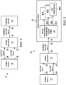
- FIG. 1 is a block diagram of an example powered system 10 according to this disclosure.
- Powered system 10 includes a power supply 12, a power balancer 14, a powered device 16, voltage rails A, B and a combined voltage rail C.
- Power supply 12 includes outputs 26, 28.
- Power balancer 14 includes inputs 30, 32, and an output 34.
- Powered device 16 includes an input 36.
- Outputs 26, 28 of power supply 12 are coupled, respectively, to inputs 30, 32 of power balancer 14 via voltage rails A, B.
- Output 34 of power balancer 14 is coupled to input 36 of powered device 16 via combined voltage rail C.
- Power supply 12 regulates each of voltage rails A, B at a respective direct current (DC) voltage level.
- the DC voltage level of voltage rail B may be different than the DC voltage level of voltage rail A.
- Power balancer 14 receives the voltages on voltage rails A, B at inputs 30, 32, respectively, and combines the voltages to generate the voltage on combined voltage rail C at output 34.
- power balancer 14 may dynamically balance the power drawn from voltage rails A, B such that the power drawn from voltage rail A substantially equals and/or is proportional to the power drawn from voltage rail B.
- Power balancer 14 may provide power to powered device 16 via combined voltage rail C.
- Powered device 16 may perform one or more device operations and/or power one or more device components based on power received from combined voltage rail C.
- power supply 12 may regulate each of voltage rails A, B at a direct current (DC) voltage level. Regulating each of voltage rails A, B at a DC voltage level may refer to outputting a respective voltage level on each of voltage rails A, B where the respective voltage level remains substantially constant over a range of load impedances. Accordingly, power supply 12 may act as a set of independent voltage sources, such as: a first independent voltage source that produces a substantially constant voltage on voltage rail A; and a second independent voltage source that produces a substantially constant voltage on voltage rail B.
- power supply 12 may be a hard disk drive (HDD) power supply that is configured to output regulated voltages suitable for powering HDD components.
- voltage rail A may be regulated at 12 volts (V)
- voltage rail B may be regulated at 5V.
- voltage rail A may be regulated at 12V
- voltage rail B may be regulated at 3.3V.
- power balancer 14 receives the voltages on voltage rails A, B and combines the voltages to generate a single output voltage on combined voltage rail C. Specifically, power balancer 14 receives a first voltage at input 30 and a second voltage at input 32, and combines the first and second voltages to generate the output voltage on combined voltage rail C. Combining the first and second voltages may refer to combining power associated with the first and second voltages to generate a combined voltage. Accordingly, power balancer 14 may transfer power from input 30 to output 34 and from input 32 to output 34 by combining power received at inputs 30, 32 into a single output power rail (i.e., combined voltage rail C).
- power balancer 14 may dynamically balance the power drawn from voltage rails A, B such that the power drawn from voltage rail A substantially equals and/or is proportional to the power drawn from voltage rail B.
- Dynamically balancing the power drawn from voltage rails A, B may include dynamically balancing the current drawn from each of voltage rails A, B such that the amount of current drawn from voltage rail B multiplied by the voltage of voltage rail B is substantially equal to and/or proportional to the amount of current drawn from voltage rail A multiplied by the voltage of voltage rail A.
- Power balancer 14 may include any circuitry configured to combine inputs 30, 32 into output 34 and/or to balance power drawn from voltage rails A, B.
- power balancer 14 may include two separate power converters with outputs coupled together and inputs coupled to respective ones of inputs 30, 32.
- the power converters may be DC-to-DC power converters, such as, e.g., buck converters, boost converters, isolated converters, and low-dropout regulators (LDOs).
- Powered device 16 may be any combination of one or more devices that are powered by combined voltage rail C.
- powered device 16 may be a solid-state drive (SSD) that includes a power management integrated circuit (PMIC) and one or more SSD components.
- PMIC power management integrated circuit
- powered device 16 may be a PMIC.
- power balancer 14 may combine power supplied by at least two different power supply rails (e.g., voltage rails A, B) into a single output power rail (i.e., combined voltage rail C).
- a single output power rail i.e., combined voltage rail C.
- power rails may allow devices that are configured to receive power via a single power supply rail to be used in legacy systems that include two different power supply rails, while still allowing such devices to draw power from each of the legacy power supply rails.
- powered devices that use a single power supply may be retrofitted into legacy systems in a relatively power-efficient manner and without requiring replacement of the existing power supply infrastructure in such systems.
- power balancer 14 may control the relative amounts of power supplied by at least two different power supply rails (e.g., voltage rails A, B) when combining the power into a single power rail. In this way, power balancer 14 may balance the amount of power drawn from each of the power supply rails to a target balancing ratio, thereby increasing the power efficiency of the system.
- power supply rails e.g., voltage rails A, B
- FIG. 2 is a block diagram of an example powered system 40 that may be used to implement powered system 10 illustrated in FIG. 1 .
- Powered system 40 includes similar components to those illustrated in FIG. 1 except that powered device 16 has been replaced by solid-state drive 42.
- solid-state drive 42 may correspond to (and be used to) implement powered device 16 illustrated in FIG. 1 .
- Solid-state drive 42 includes a power management integrated circuit (PMIC) 44, SSD components 46A, 46B, 46C (collectively, “SSD components 46"), and an input 48.
- PMIC power management integrated circuit
- SSD components 46A, 46B, 46C collectively, “SSD components 46”
- input 48 is coupled to output 34 of power balancer 14 via combined voltage rail C.
- PMIC 44 includes an input 50 that is coupled to output 34 of power balancer 14 via combined voltage rail C. Input 50 may correspond to input 48 of solid-state drive 42. PMIC 44 also includes outputs 52A, 52B, 52C (collectively, “outputs 52"). Each of outputs 52 is coupled to a respective one of SSD components 46.
- Solid-state drive 42 may store and retrieve data for a client system. Solid-state drive 42 may be powered completely or at least in part by combined voltage rail C. Because power balancer 14 transfers power from power supply 12 to combined voltage rail C, solid-state drive 42 may also said to be powered completely or in part by voltage rail A and voltage rail B of power supply 12.
- PMIC 44 may receive power via input 50, and manage the distribution of received power to SSD components 46 via outputs 52. Managing the distribution of received power to SSD components 46 may involve outputting a regulated voltage on each of outputs 52. The regulated voltages output on each of outputs 52 may be the same or different. In some examples, PMIC 44 may perform one or more of the following functions: power management, voltage regulation, DC-to-DC conversion, voltage scaling, dynamic voltage scaling, dynamic frequency scaling, and power sequencing.
- solid-state drive 42 may store data without using a motor or mechanically spinning disks.
- solid-state drive 42 may store data using a memory array and/or an integrated circuit array that is accessed via an electronic interface.
- SSD components 46 may receive power from PMIC 44 via a respective one of power lines coupled to outputs 52.
- SSD components 46 may be any components that assist in the operation of solid-state drive 42.
- SSD components 46 may include one or more of controllers, memory arrays, integrated circuit storage arrays, and other components used by an SSD.
- power supply 12 may be an HDD power supply that is configured to output voltages suitable for powering an HDD.
- power supply 12 may output a 12V voltage on voltage rail A and either 5V or 3.3V voltage on voltage rail B.
- voltage rails A, B may be referred to as HDD power supply rails.
- power balancer 14 uses two power converters to combine two separate HDD power supply rails (e.g., voltage rails A, B) of powered system 40 into a single, regulated output voltage rail (e.g., combined voltage rail C) that is suitable for use by PMIC 44 and/or SSD components 46.
- each of the two power converters may have an input that is coupled to a respective power supply rail (e.g., voltage rails A, B), and the outputs of the power converters may be coupled together to generate a single output voltage rail for PMIC 44 and/or SSD components 46.
- Combining HDD power supply rails in this manner may allow legacy HDD power distribution systems (e.g., voltage rails A, B) to be used to power solid-state drive 42, while at the same time allowing solid-state drive 42 to draw power from each of the legacy HDD power supply rails.
- legacy HDD power distribution systems e.g., voltage rails A, B
- solid-state drive 42 may be retrofitted into legacy HDD systems in a relatively power-efficient manner and without requiring replacement of the existing HDD power supply infrastructure.
- the techniques in this disclosure may be used to actively balance power between two HDD power supply inputs that are combined into a single output voltage rail. Operating two power converters in this manner may allow the power drawn from each of the HDD power supply rails to be dynamically balanced at a particular ratio and/or equalized during operation of solid-state drive 42. In this way, the power efficiency of a retrofitted SSD drive may be improved compared to systems that statically allocate SSD components to individual HDD power rails based on worst case power consumption estimates. Also, in some examples, the techniques of this disclosure may simplify power design across platforms by making a unified output, which may feed all downstream supplies.
- FIG. 3 is a block diagram of an example power balancer 14 that may be used in the powered systems of FIGS. 1 and 2 . Although usable in either of the systems of FIGS. 1 and 2 , for purposes of explanation, power balancer 14 of FIG. 3 will be illustrated and described as being used in powered system 40 of FIG. 2 .
- Power balancer 14 includes power converters 54, 56.
- Power converter 54 includes an input 58 and an output 60.
- Power converter 56 includes an input 62 and an output 64.
- Input 58 is coupled to voltage rail A, and input 62 is coupled to voltage rail B.
- Output 60 is coupled to output 64, and both of outputs 60, 64 are coupled to input 50 of PMIC 44.
- Power converter 54 may receive power at input 58 and transfer some or all of the received power to output 60 for use by PMIC 44.
- Power converter 56 may receive power at input 62 and transfer some or all of the received power to output 64 for use by PMIC 44.
- each of power converters 54, 56 may convert the voltage received at their respective inputs 58, 62 to other respective voltages, and output the respective voltages at outputs 60, 64. Similarly, each of power converters 54, 56 may convert the current received at their respective inputs 58, 62 to other respective currents, and output the respective currents at outputs 60, 64. Accordingly, power converters 54, 56 may convert the form of power received at inputs 58, 62 to another form of power at outputs 60, 64.
- power converter 54 may regulate the voltage produced at output 60 such that the voltage is substantially equal to and/or proportional to a reference voltage.
- the reference voltage may correspond to and/or be proportional to a specified power rail voltage for PMIC 44.
- power converter 56 may regulate the current produced at output 64 such that the amount of current produced by power converter 56 at output 64 is substantially equal to and/or proportional to the amount of current produced by power converter 54 at output 60.
- each of power converters 54, 56 may be a DC-to-DC converter.
- power converters 54, 56 may be any combination of buck converters (e.g., synchronous buck converters), boost converters, isolated converters, low-dropout (LDO) regulators, linear power converters (e.g., linear voltage regulators), switching power converters (e.g., switching voltage regulators), or other DC-to-DC converters.
- buck converters e.g., synchronous buck converters
- boost converters isolated converters
- LDO low-dropout
- linear power converters e.g., linear voltage regulators
- switching power converters e.g., switching voltage regulators
- power balancer 14 may be used to combine power rails that are associated with power supplies in HDD type systems.
- Using two power converters 54, 56 to combine HDD power supply rails in the manner shown by FIG. 3 may allow legacy HDD power distribution systems to be used to power PMIC 44 (and corresponding SSD data storage devices), while at the same time allowing the SSD data storage devices to draw power from each of the legacy HDD power supply rails.
- SSDs may be retrofitted into legacy HDD systems in a relatively power-efficient manner and without requiring replacement of the existing HDD power supply and distribution infrastructure.
- combining the power rails in this manner may simplify power design across platforms by making a unified output which may feed, in some cases, all downstream supplies.
- Another technique for retrofitting HDD type systems with SSDs involves using two separate power chains with two separate power converters and two separate PMICs (i.e., one power converter and PMIC for each power rail).
- a system designer may statically allocate approximately half the load to the 5V rail and approximately half the load to the 12V rail. Doing so may keep the total power under the power envelope requirements.
- this technique may not be ideal because the power drawn from each of the rails may not be perfectly balanced between 12V rails and 5V rails due to non-idealities in the converters and/or due to dynamics in the various loads.
- Causing power converter 56 to regulate the current at output 64 such that it is substantially the same as and/or proportional to the amount of current output by power converter 54 at output 60 may allow power balancer 14 to actively and dynamically balance power between two HDD power supply inputs that are combined into a single output voltage rail.
- Operating two power converters 54, 56 in this manner may allow the power drawn from each of the power supply rails to be dynamically balanced at a particular ratio and/or equalized during operation of the SSD. In this way, the power efficiency of a retrofitted SSD drive may be improved compared to systems that statically allocate SSD components to individual HDD power rails based on worst case power consumption estimates.
- FIG. 4 is a block diagram of another example power balancer 80 according to this disclosure.
- Power balancer 80 may be used to implement any of power balancers 14 illustrated in FIGS. 1-3 .
- Power balancer 80 includes power converters 82, 84, power converter control circuits 86, 88, and current sensing circuits 90, 92.
- Power converter 82 includes a voltage input 94, a control input 96, and an output 98.
- Power converter 84 also includes a voltage input 100, a control input 102, and an output 104.
- Power converter control circuit 86 includes a reference input 106, a feedback input 108, and an output 110.
- Power converter control circuit 88 also includes a reference input 112, a feedback input 114, and an output 116.
- Current sensing circuit 90 includes an input 118, and an output 120.
- Current sensing circuit 92 also includes an input 122 and an output 124.
- Voltage input 94 of power converter 82 is coupled to input voltage A.
- Voltage input 100 of power converter 84 is coupled to input voltage B.
- Output 98 of power converter 82 is coupled to output 104 of power converter 84.
- Outputs 98, 104 of power converters 82, 84 may form an output voltage for power balancer 80.
- Input voltage A, input voltage B, and the output voltage may correspond, respectively, to voltage rail A, voltage rail B, and combined voltage rail C in FIGS. 1 and 2 .
- input voltage A may form input 30 for power balancer 14 shown in any of FIGS. 1-3
- input voltage B may form input 32 for power balancer 14
- the output voltage may form output 34 for power balancer 14 shown in any of FIGS. 1-3 .
- Reference input 106 of power converter control circuit 86 is coupled to input voltage A.
- Feedback input 108 of power converter control circuit 86 is coupled to output 98 of power converter 82.
- Output 110 of power converter control circuit 86 is coupled to control input 96 of power converter 82.
- Output 98 of power converter 82 is coupled to input 118 of current sensing circuit 90.
- Output 120 of current sensing circuit 90 is coupled to reference input 112 of power converter control circuit 88.
- Output 104 of power converter 84 is coupled to input 122 of current sensing circuit 92.
- Output 124 of current sensing circuit 92 is coupled to feedback input 114 of power converter control circuit 88.
- Output 116 of power converter control circuit 88 is coupled to control input 102 of power converter 84.
- Power converter 82 may receive power at voltage input 94 and transfer some or all of the received power to output 98.
- Power converter 84 may receive power at voltage input 100 and transfer some or all of the received power to output 104.
- Collectively, power converters 82, 84 may combine the powered received at voltage inputs 92, 100 into a single power rail that supplies the output voltage for power balancer 80.
- Power converter control circuit 86 receives via feedback input 108 a signal indicative of the voltage at output 98 of power converter 82. Power converter control circuit 86 also receives a reference voltage signal via reference input 106. Power converter control circuit 86 generates a control signal based on the signal indicative of the voltage at output 98 of power converter 82 and the reference voltage signal. Power converter control circuit 86 may generate the control signal such that the control signal causes power converter 82 to regulate output 98 of power converter 82 at a voltage level that is equal to and/or proportional to the reference voltage received via reference input 106. Power converter control circuit 86 outputs the control signal at output 110, which is received by power converter 82 at control input 96.
- Current sensing circuit 90 generates a signal indicative of the amount of current produced by power converter 82 at output 98, and outputs the signal indicative of the amount of current via output 120.
- current sensing circuit 92 generates a signal indicative of the amount of current produced by power converter 84 at output 104, and outputs the signal indicative of the amount of current via output 124.
- Power converter control circuit 88 receives via reference input 112 the signal indicative of the amount of current produced by power converter 82. Power converter control circuit 88 receives via feedback input 114 the signal indicative of the amount of current produced by power converter 84. Power converter control circuit 88 generates a control signal based on the signal indicative of the current produced by power converter 82 and the signal indicative of the current produced by power converter 84. Power converter control circuit 88 may generate the control signal such that the control signal causes power converter 84 to regulate the amount of current produced at output 104 at a level that is substantially equal to and/or proportional to the amount of current produced at output 98 of power converter 82. Power converter control circuit 88 outputs the control signal at output 116, which is received by power converter 84 at control input 102.
- Power converter control circuit 86 and power converter 82 may together regulate the voltage level of the output voltage of power converter 82 at a voltage level that is equal to or proportional to the reference voltage.
- Power converter control circuit 88 and power converter 84 may together balance the currents that are output by each of power converters 82, 84 such that the amount of current output by power converter 84 substantially equals and/or is proportional to the amount of current output by power converter 82.
- the reference voltage may be supplied internally by power balancer 80 or may be an external input to power balancer 80.
- the reference voltage may be indicative of a voltage at which output 98 of power converter 82 is to be regulated.
- the voltage at which output 98 is to be regulated may correspond to and/or be proportional to a power supply voltage requirement or specification for a PMIC or other powered device that is powered by power balancer 80.
- the signal indicative of the voltage at output 98 of power converter 82 may be the actual voltage at output 98.
- output 98 may be directly coupled or electrically coupled to feedback input 108.
- inputs 118, 122 of current sensing circuits 90, 92 may be magnetically coupled, respectively to outputs 98, 104 of power converters 82, 84. In further examples, inputs 118, 122 of current sensing circuits 90, 92 may be directly coupled, respectively to outputs 98, 104 of power converters 82, 84.
- current sensing circuits 90, 92 may each include one or more sensing elements (e.g., resistors) that are placed along current paths between outputs 98, 104 of power converters 82, 84 and the output of power balancer 80.
- sensing elements e.g., resistors
- output 98 of power converter 82 when output 98 of power converter 82 is said to be coupled to output 104 of power converter 84, output 98 may be coupled to output 104 through the one or more sensing elements that are placed in series along the current paths between outputs 98, 104 and the output of power balancer 80.
- power converter control circuit 86 may generate a control signal such that the control signal causes power converter 82 to regulate output 98 of power converter 82 at a level that is equal to and/or proportional to the reference voltage received via reference input 106.
- the control signal may be a function of and/or indicative of a difference between the signal received at feedback input 108 and the reference voltage received at reference input 106.
- the control signal may be equal to the difference between the signal received at feedback input 108 and the reference voltage received at reference input 106.
- control signal may be a filtered version of the difference between the signal received at feedback input 108 and the reference voltage received at reference input 106 (e.g., a proportional-integral (PI) filtered version of the difference between the signal received at feedback input 108 and the reference voltage received at reference input 106).
- PI proportional-integral
- power converter control circuit 88 may generate a control signal such that the control signal causes power converter 84 to regulate the amount of current produced at output 104 at a level that is substantially equal to and/or proportional to the amount of current produced at output 98 of power converter 82.
- the control signal may be a function of and/or indicative of a difference between the signals received at reference input 112 and feedback input 114.
- the control signal may be equal to the difference between the signals received at reference input 112 and feedback input 114.
- the control signal may be a filtered version of the difference between the signals received at reference input 112 and feedback input 114 (e.g., a PI filtered version of the difference between the signals received at reference input 112 and feedback input 114).
- each of power converters 54, 56 may be a DC-to-DC converter.
- power converters 54, 56 may be any combination of buck converters (e.g., synchronous buck converters), boost converters, isolated converters, low-dropout (LDO) regulators, linear power converters (e.g., linear voltage regulators), switching power converters (e.g., switching voltage regulators), or other DC-to-DC converters.
- Power converters 54, 56 need not by the same type of power converter.
- control signals output by power converter control circuits 86, 88 may control the amount of power and/or current passed by the pass element.
- the control signal may control the gate of a transistor.
- the amplitude of the control signal output by power converter control circuit 86 may vary based on the difference between the voltage at output 98 of power converter 82 and the reference voltage.
- the amplitude of the control signal output by power converter control circuit 88 may vary based on the difference between the amount current produced at output 98 of power converter 82 and the amount of current produced at output 104 of power converter 84.
- the control signals output by power converter control circuits 86, 88 may be used for regulating the on resistance of respective pass transistors in each of power converters 82, 84.
- the duty cycle of the control signal output by power converter control circuit 86 may vary based on the difference between the voltage at output 98 of power converter 82 and the reference voltage.
- the duty cycle of the control signal output by power converter control circuit 88 may vary based on the difference between the amount current produced at output 98 of power converter 82 and the amount of current produced at output 104 of power converter 84.
- the control signals output by power converter control circuits 86, 88 may be used for regulating the duty cycle of relatively high frequency signals that are coupled to respective pass transistors in each of power converters 82, 84.
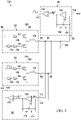
- FIG. 5 is a schematic diagram of an example power balancer 130 that may be used to implement power balancer 80 illustrated in FIG. 4 according to this disclosure. Same or similar components between FIGS. 4 and 5 have been numbered with identical reference numerals.
- Power converter 82 includes a high-side transistor 132, a low-side transistor 134, an inductor 136, gate drivers 138, 140, and an inverter 142.
- High-side transistor 132 includes: (a) a drain terminal coupled to voltage input 94, (b) a gate terminal coupled to an output of gate driver 138, and (c) a source terminal coupled to a drain terminal of low-side transistor 134 and a first terminal of inductor 79.
- Low-side transistor 134 includes: (a) a drain terminal coupled to the source terminal of high-side transistor 132 and the first terminal of inductor 136, (b) a gate terminal coupled to an output of gate driver 140, and (c) a source terminal coupled to a ground reference voltage.
- Gate driver 138 includes an input coupled to control input 96, and an output coupled to the gate of high-side transistor 132.
- Inverter 142 includes an input coupled to control input 96, and an output coupled to an input of gate driver 140.
- Gate driver 140 includes an input coupled to the output of inverter 142, and an output coupled to the gate of low-side transistor 134.
- Inductor 136 includes a first terminal coupled to the source of high-side transistor 132 and to the drain of low-side transistor 134. Inductor 136 further includes a second terminal coupled to output 98.
- Power converter 84 includes transistors 144, 146, an inductor 148, gate drivers 150, 152, and an inverter 154.
- the components in power converter 84 are the same as those in power converter 82 and are arranged in a similar configuration. Accordingly, the arrangement of these components will not be described in further detail.
- Power balancer 130 further includes a capacitor 156.
- Capacitor 156 includes: (a) a first terminal coupled to output 98 of power converter 82 and to output 104 of power converter 84, and (b) a second terminal coupled to a ground reference voltage. Although capacitor 156 is illustrated as being outside of power converters 82, 84, in other examples, capacitor 156 may form a part of one or both of power converters 82, 84. Each of power converters 82, 84 in power balancer 130 may be a synchronous buck converter.
- Power converter control circuit 86 includes operational amplifiers 158, 160, capacitors 162, 164, and a resistor 166.
- Operational amplifier 158 includes: (a) a non-inverting input coupled to reference input 106, (b) an inverting input coupled to feedback input 108, to a first terminal of capacitor 162, and to a first terminal of capacitor 164, and (c) an output coupled to a non-inverting input of operational amplifier 160, a second terminal of capacitor 162, and a first terminal of resistor 166.
- Operational amplifier 160 includes: (a) an inverting input coupled to a sawtooth waveform signal, (b) a non-inverting input coupled to the output of operational amplifier 158, and (c) an output coupled to output 110.
- a second terminal of capacitor 164 is coupled to a second terminal of resistor 166.
- another type of amplifier or differential amplifier may be substituted for one or both of operational amplifiers 158, 160 and/or for one or more of any of the other operational amplifiers described in this disclosure.
- Operational amplifier 158, capacitors 162, 164, and resistor 166 may form a proportional-integral (PI) filter that generates a filtered difference between reference input 106 and feedback input 108.
- Operational amplifier 160 may form a signal generator that generates a control signal for power converter 82 based on the filtered difference between reference input 106 and feedback input 108.
- PI proportional-integral
- Power converter control circuit 88 includes operational amplifiers 168, 170, capacitors 172, 174, and a resistor 176.
- the components in power converter control circuit 88 are the same as those in power converter control circuit 86 and are arranged in a similar configuration. Accordingly, the arrangement of these components will not be described in further detail.
- Power converter 82 transfers power from input voltage A to output 98 based on a control signal received at control input 96.
- the voltage at output 98 may be determined at least in part based on the duty cycle of control input 96.
- the control signal alternatively switches transistors 132, 134 on and off in a synchronous buck converter-like fashion to transfer power from voltage input 94 to output 98.
- Power converter control circuit 86 generates a control signal to regulate the voltage at output 98 of power converter 82 at a voltage level determined by the reference voltage.
- the PI filter formed by operational amplifier 158, capacitors 162, 164, and resistor 166 compares the output voltage at output 98 of power converter 82 to the reference voltage, and generates a signal indicative of a filtered difference between the output voltage at output 98 of power converter 82 and the reference voltage.
- Power converter control circuit 86 generates the control signal based on the signal indicative of the filtered difference between the output voltage of power converter 82 (i.e., the output voltage at output 98) and the reference voltage.
- operational amplifier 160 compares the signal indicative of the filtered difference between the output voltage of power converter 82 and the reference voltage to a sawtooth waveform, and generates a signal indicative of whether the signal indicative of the filtered difference between the output voltage of power converter 82 and the reference voltage is greater than or less than the sawtooth waveform at any given moment in time. This causes the duty cycle of the resulting signal to reflect the filtered difference between the output voltage of power converter 82 and the reference voltage.
- the control loop formed by power converter control circuit 86 causes power converter 82 to regulate output 98 at a constant output voltage that is substantially equal to the reference voltage. If the output voltage at output 98 were to become greater than the reference voltage, then the output of the PI filter formed by operational amplifier 158, capacitors 162, 164, and resistor 166 would increase, thereby causing the duty cycle of the control signal to decrease, which in turn would cause power converter 82 to decrease the voltage at output 98.
- Power converter 84 transfers power from input voltage B to output 104 based on a control signal received at control input 102.
- the current produced by power converter 84 at output 104 may be determined at least in part based on the duty cycle of control input 102.
- the control signal alternatively switches transistors 144, 146 on and off in a synchronous buck converter-like fashion to transfer power from voltage input 100 to output 104.
- Current sensing circuit 90 generates a signal indicative of the current produced at output 98 of power converter 82.
- Current sensing circuit 92 generates a signal indicative of the current produced at output 104 of power converter 84.
- Power converter control circuit 88 generates a control signal to regulate the current produced at output 104 of power converter 84 such that the amount of current produced at output 104 of power converter 84 is substantially equal to the amount of current produced at output 98 of power converter 82.
- the PI filter formed by operational amplifier 168, capacitors 172, 174, and resistor 176 compares the signal indicative of the current produced at output 104 of power converter 84 to the signal indicative of the current produced at output 98 of power converter 82, and generates a signal indicative of a filtered difference between the currents.
- Power converter control circuit 88 generates the control signal based on the signal indicative of the filtered difference between the currents.
- operational amplifier 170 compares the signal indicative of the filtered difference between the currents to a sawtooth waveform, and generates a signal indicative of whether the signal indicative of the filtered difference between the currents is greater than or less than the sawtooth waveform at any given moment in time. This causes the duty cycle of the resulting signal to reflect the filtered difference between the output currents produced by power converters 82, 84.
- the control loop formed by power converter control circuit 88 causes power converter control circuit 88 to regulate the amount current produced at output 104 at an amount of current that is approximately equal to the amount of current produced at output 98 of power converter 82. If the output current produced at output 104 were to become greater than the output current produced at output 98, then the output of the PI filter formed by operational amplifier 168, capacitors 172, 174, and resistor 176 would increase, thereby causing the duty cycle of the control signal to decrease, which in turn would cause power converter 84 to decrease the amount of current produced at output 104.
- power converter 84 and power converter control circuit 88 operate together to regulate the amount of current produced by power converter 82 at output 104 to substantially match the amount of current produced by power converter 84 at output 98.
- power balancer 130 may combine two input voltages provided by two power supply rails into a single, regulated output voltage supply rail.
- Power balancer 130 may regulate the output voltage supply rail at the reference voltage, and may control power converters 82, 84 such that the amount of current drawn from each of power converters 82, 84 is approximately equal.
- power converter control circuit 86 may balance the power drawn from each of the two power supply rails.
- FIG. 6 is a schematic diagram of an example power balancer 180 according to this disclosure.
- power balancer 180 may be used to implement the power balancers illustrated in FIGS. 1 or 2 .
- Power balancer 180 in FIG. 6 is similar to power balancer 130 shown in FIG. 5 except that an additional power converter 182, power converter control circuit 184, and current sensing circuit 186 have been added. Same or similar components between FIGS. 5 and 6 have been numbered with identical reference numerals.
- Power converter 182 includes a high-side transistor 188, a low-side transistor 190, an inductor 192, gate drivers 194, 196, and an inverter 198.
- Power converter control circuit 184 includes operational amplifiers 200, 202, capacitors 204, 206, and a resistor 208.
- Power converter 182 further includes a voltage input 210, a control input 212, and an output 214.
- Power converter control circuit 184 further includes a reference input 216, a feedback input 218, and an output 220.
- Voltage input 210 of power converter 182 is coupled to input voltage C.
- Control input 212 of power converter 182 is coupled to output 220 of power converter control circuit 184.
- Output 214 of power converter 182 is coupled to output 98 of power converter 82 and output 104 of power converter 84. Output 214, output 98, and output 104 may form the output voltage supply rail for power balancer 180.
- Current sensing circuit 186 includes an input coupled to output 214 of power converter 182, and an output coupled to feedback input 218 of power converter control circuit 184.
- Current sensing circuit 186 generates a signal indicative of the current produced at output 214 of power converter 182.
- Reference input 216 is coupled to the output of current sensing circuit 92, and feedback input 218 is coupled to the output of current sensing circuit 186.
- power converter control circuit 86 and power converter 82 regulate the voltage at output 98 such that the voltage is substantially equal to the reference voltage.
- Power converter control circuit 88 and power converter 84 regulate the amount of current produced at output 104 such that the amount of the amount of current produced at output 104 of power converter 84 is substantially equal to the amount of current produced at output 98 of power converter 82.
- Power converter control circuit 184 and power converter 182 regulate the amount of current produced at output 214 such that the amount of the amount of current produced at output 214 of power converter 182 is substantially equal to the amount of current produced at output 104 of power converter 84.
- power balancer 180 may combine three different input power rails while balancing the power drawn from each of the power rails.
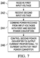
- FIG. 7 is a flow diagram of an example technique for combining and balancing power according to this disclosure.
- the technique illustrated in FIG. 7 may be used in any of the systems or power converters described in this disclosure.
- Power balancer 14 receives a first voltage at a first input (240). Power balancer 14 receives a second voltage at a second input (242). In some examples, the voltage level of the first voltage is different than a voltage level of the second voltage. Power balancer 14 combines, with power converters 82, 84, power received from the first and second inputs (i.e., received from the first and second input voltages) into a single power rail (244). Power balancer 18 controls power converter 84 such that power converter 84 outputs an amount of current to the single power rail that is proportional to an amount of current output to the single power rail by power converter 82 (246). In some examples, power balancer 14 may control power converters 82, 84 such that each of power converters 82, 84 outputs a same amount of current to the single power rail
- this disclosure describes an integrated circuit (e.g., power balancers 14, 80) that includes a first input 30, a second input 32, and an output 34.
- the integrated circuit includes a power converter 82 having: (a) a voltage input 94 coupled to input 30 of the integrated circuit, (b) a control input 96, and (c) an output 98 coupled to output 34 of the integrated circuit.
- the integrated circuit further includes a power converter 84 having: (a) a voltage input 100 coupled to input 32 of the integrated circuit, (b) a control input 102, and (c) an output 104 coupled to output 98 of power converter 82 and to output 34 of the integrated circuit.
- the integrated circuit further includes a power converter control circuit 86 having: (a) a reference input 106 coupled to a reference voltage lead, (b) a feedback input 108 coupled to output 98 of power converter 82, and (c) an output 110 coupled to control input 96 of power converter 82.
- the integrated circuit further includes a power converter control circuit 88 having: (a) a reference input 112, (b) a feedback input 114, and (c) an output 116 coupled to control input 102 of power converter 84.
- the integrated circuit further includes a current sensing circuit 90 having: (a) an input 118 coupled to output 98 of power converter 82, and (b) an output 120 coupled to reference input 112 of power converter control circuit 88.
- the integrated circuit further includes a current sensing circuit 92 having: (a) an input 122 coupled to output 104 of power converter 84, and (b) an output 124 coupled to the feedback input 114 of power converter control circuit 88.
- voltage input 94 of power converter 82 is free of connection to voltage input 100 of power converter 84.
- power converter control circuit 88 is free of connection to the reference voltage lead and/or the reference voltage.
- power converters 82, 84 are buck converters. In further examples, power converters 82, 84 are low-dropout regulators (LDOs).
- LDOs low-dropout regulators
- power converter 82 is a first type of power converter
- power converter 84 is a second type of power converter.
- power converter 82 may be a buck converter
- power converter 84 may be an LDO.
- power converter 82 may be an LDO
- power converter 84 may be a buck converter.
- Other types of power converters include buck converters (e.g., synchronous buck converters, non-synchronous buck converters), boost converters, isolated converters, low-dropout (LDO) regulators, linear power converters (e.g., linear voltage regulators), switching power converters (e.g., switching voltage regulators), or other DC-to-DC converters.
- input 118 of current sensing circuit 90 is magnetically coupled to output 98 of power converter 82, and input 122 of current sensing circuit 92 is magnetically coupled to output 104 of power converter 84.
- input 118 of current sensing circuit 90 is electrically coupled to output 98 of power converter 82, and input 122 of current sensing circuit 92 is electrically coupled to output 104 of power converter 84
- power converter 82 and power converter control circuit 86 regulate a voltage produced at output 98 of power converter 82 such that a magnitude of the voltage is proportional to a magnitude of the reference voltage.
- power converter 84 and power converter control circuit 88 regulate a current produced at output 104 of power converter 84 such that a magnitude of the current is proportional to a magnitude of a current produced at output 98 of power converter 82.
- power converter 82 and power converter control circuit 86 regulate a voltage produced at output 98 of power converter 82 such that a magnitude of the voltage is equal to a magnitude of the reference voltage.
- power converter 84 and power converter control circuit 88 regulate a current produced at output 104 of power converter 84 such that a magnitude of the current is equal to a magnitude of a current produced at output 98 of power converter 82.
- the integrated circuit may be part of a powered system that further includes a powered device 16 (e.g., FIGS. 1 and 2 ) having input 36 coupled to each of the outputs 98, 104 of power converters 82, 84.
- powered device 16 is a PMIC 44.
- the powered device may be a solid-state drive, and PMIC 44 is coupled to one or more of SSD components 46.
- the powered system may include a power supply 12 (e.g., FIGS. 1 and 2 ) having an output 26 coupled to voltage input 94 of power converter 82, and an output 28 coupled to output 98 of power converter 84.
- power supply 12 may be configured to output a first voltage at output 26 of power supply 12 and a second voltage at output 28 of power supply 12, and the magnitude of the first voltage may be different than the magnitude of the second voltage.
- this disclosure describes, as shown for example in FIGS. 2 and 3 , a device that includes a power converter 54 having an input 58 and an output 60.
- the device further includes a power converter 56 having an input 62 and an output 64.
- the device further includes a PMIC 44 having an input 50 coupled to outputs 60, 64 of power converters 54, 56.
- the device further includes one or more data storage device components (e.g., SSD components 46) coupled to PMIC 44.
- input 62 of power converter 56 is free of connection to input 58 of power converter 54.
- power converters 54, 56 are buck converters. In further examples, power converters 54, 56 are low-dropout regulators (LDOs). In additional examples, power converter 54 is a first type of power converter, and power converter 56 is a second type of power converter.
- LDOs low-dropout regulators
- power converter 54 is configured to regulate a voltage produced at output 60 of power converter 54 such that a magnitude of the voltage is proportional to a magnitude of the reference voltage.
- power converter 56 is configured to regulate a current produced at output 64 of power converter 56 such that a magnitude of the current corresponds to a magnitude of a current produced at output 60 of power converter 54.
- power converter 56 is configured to regulate the current produced at output 64 of power converter 56 without using a signal indicative of the voltage at output 64 of power converter 56.
- this disclosure describes a device that includes a power converter 82 having a voltage input 94 and an output 98.
- the device further includes a power converter 84 having a voltage input 100 and an output 104.
- Output 104 of power converter 84 is coupled to output 98 of power converter 82.
- the device further includes first control circuitry (e.g., power converter control circuit 86) configured to control power converter 82 based on a signal indicative of the voltage at the output of the first power converter and a reference voltage.
- the device further includes second control circuitry (e.g., power converter control circuit 88) configured to control the second power converter based on a signal indicative of a current at output 98 of power converter 82 and a signal indicative of a current at output 104 of power converter 84.
- second control circuitry e.g., power converter control circuit 88
- voltage input 100 of power converter 84 is free of connection to voltage input 94 of power converter 82.
- the second control circuitry controls the output 104 without using a signal indicative of a voltage at output 104 of power converter 84. In further examples, the second control circuitry controls power converter 84 without using a signal indicative of the reference voltage.
- each of the power balancer circuits described in this disclosure may be implemented on a single integrated circuit where the inputs of the respective power balancer circuit are coupled to respective input pins of the integrated circuit and the output of the respective power balancer circuit is coupled to output pins of the integrated circuit.
- This disclosure describes control techniques to combine two voltage inputs into one voltage output with control of the amount of current that is supplied from each voltage input.
- the techniques may include combining two independent input voltages into a single regulated output voltage.
- SSDs solid-state drives
- PMIC power management integrated circuit
- One technique for dealing with retrofitting HDD type systems with SSDs is to roughly allocate half the load to the 5V rail and half the load to the 12V rail. Doing so may maximize the usable power consumption by keeping total power under the necessary power envelope. However this technique may not be ideal as the power is not perfectly balanced between 12V rails and 5V rails due to non-idealities in the converters and due to dynamics in the various loads.
- This disclosure describes techniques for actively balancing power between the two inputs and for combining the inputs into a single output suitable for SSD PMICs.
- the techniques of this disclosure may use two power converters, one for the 12V rail and one for the 5V rail, the output of each converter may be combined into a single, regulated output.
- the 12V rail converter regulates it output voltage to a reference.
- the 5V rail converter regulates its output current to match, or be a percentage of, the 12V converters output current. In this way, the two input voltages can be combined onto a single regulated output with power drawn from each rail controlled by the 5V power converter.
- the techniques described in this disclosure may be capable of actively balancing current between two separate inputs and combining them to a single rail.
- Other techniques may include using both rails as separate with only very rough (not active) current balancing.
- One technique for retrofitting HDD type systems with SSDs is to use two separate PMICs (i.e., one for each power rail) and to statically allocate approximately half the load to the 5V rail and approximately half the load to the 12V rail. Accordingly, rather than combining the two inputs onto a single rail, the technique may maintain two separate rails, which are individually regulated. Such a technique may have one or more drawbacks.
- the amount of power may need to be equally distributed from the two inputs. To do so, an engineer may need to roughly partition the worst case loads such that one half are on one rail, the other half are on the second rail. Such partitioning may be a significant design challenge, and may lead to inaccuracies.
- Second, performing a static allocations based on worst case power estimates may reduce the ability flexibility to port this design to other products or product families. Because the loads may need to be roughly equally balanced among the two input voltages, the system needs to be redesigned with every next generation.
- the techniques described in this disclosure may allow a user to increase their power envelope. Rather than being limited by the ability to balance powers (as with some other techniques), the techniques of this disclosure may make sure power delivered from each source is the same so that the total power envelope can be closer approached. Also, the techniques of this disclosure may simplify power design across platforms by making a unified output which may feed, in some cases, all downstream supplies.
- power balancer 14 may use two power converters 54, 56 to combine two separate inputs into a single, voltage regulated output.
- power balancer 14 may control one buck converter to regulate its output voltage.
- Power balancer 14 may regulate the other buck converter such that the output current matches the output current of the other buck converter.
- Power converters 54, 56 in FIG. 3 may be any type converters, including boost converters, LDOs, isolated converters, and other converters.
- the techniques of this disclosure may combine two input voltage sources into one, regulated output voltage source, while maintaining the output current of a first power converter equal to the output current of a second power converter.
- power converter 82 may be supplied by a first input voltage, VIN1.
- the output voltage of power converter 82 may be regulated by first measuring the output voltage and comparing it to a reference, VREF.
- Power converter control circuit 86 may use a compensation network (e.g., a proportional-integral (PI) compensation network as formed by operational amplifier 158, capacitors 162, 164 and resistor 166 as shown in FIG. 5 ) to generate a compensated error signal (e.g., output of operational amplifier 158), which is fed to a comparator (e.g., operational amplifier 162).
- the comparator compares the compensated error to a sawtooth to generate a square wave with a duty cycle.
- the duty cycle controls the output voltage to regulate VOUT to VREF by adjustment of the compensated error signal.
- Power converter control circuit 88 may measure the current produced by power converter 82 and the current produced by power converter 84. The output current of power converter 82 becomes the reference for controlling power converter 84. In a similar manner, the control loop (e.g., formed by power converter control circuit 88) adjusts the duty cycle of the control signal power converter 84 so that its output current equals the output current of power converter 82.
- the control loop e.g., formed by power converter control circuit 88
- the current sensing performed by current sensing circuits 90, 92 and current sensing circuit 186 may be performed using any of variety of techniques, both internal to the chip and external to the chip.
- power converters 82, 84 are depicted as buck converters in FIG. 5 , other power converters for processing power may be used, including, e.g., switching regulators or LDOs.
- the power switches may be internal to the chip or external to the chip
- FIGS. 3-5 illustrate the techniques of this disclosure as being implemented with two power converters, the techniques of this disclosure may also be implemented with more than two power converters, as shown, e.g., in FIG. 6 .
- the third power converter e.g., power converter 182
- the power combination and balancing techniques of this disclosure may be scalable to a higher and/or lower number of power converters.
- the techniques and circuitry described in this disclosure may be implemented on any combination of one or more integrated circuits.
Landscapes
- Engineering & Computer Science (AREA)
- Power Engineering (AREA)
- Physics & Mathematics (AREA)
- General Physics & Mathematics (AREA)
- Theoretical Computer Science (AREA)
- Electromagnetism (AREA)
- Radar, Positioning & Navigation (AREA)
- Automation & Control Theory (AREA)
- General Engineering & Computer Science (AREA)
- Dc-Dc Converters (AREA)
- Direct Current Feeding And Distribution (AREA)
Applications Claiming Priority (3)
| Application Number | Priority Date | Filing Date | Title |
|---|---|---|---|
| US201562127069P | 2015-03-02 | 2015-03-02 | |
| US14/719,575 US9880574B2 (en) | 2015-03-02 | 2015-05-22 | Power combiner and balancer |
| PCT/US2016/020469 WO2016141070A1 (en) | 2015-03-02 | 2016-03-02 | Power combiner and balancer |
Publications (3)
| Publication Number | Publication Date |
|---|---|
| EP3286813A1 EP3286813A1 (en) | 2018-02-28 |
| EP3286813A4 EP3286813A4 (en) | 2018-06-20 |
| EP3286813B1 true EP3286813B1 (en) | 2023-01-25 |
Family
ID=56848651
Family Applications (1)
| Application Number | Title | Priority Date | Filing Date |
|---|---|---|---|
| EP16759419.1A Active EP3286813B1 (en) | 2015-03-02 | 2016-03-02 | Power combiner and balancer |
Country Status (5)
| Country | Link |
|---|---|
| US (4) | US9880574B2 (enExample) |
| EP (1) | EP3286813B1 (enExample) |
| JP (1) | JP6824182B2 (enExample) |
| CN (1) | CN107251355B (enExample) |
| WO (1) | WO2016141070A1 (enExample) |
Families Citing this family (25)
| Publication number | Priority date | Publication date | Assignee | Title |
|---|---|---|---|---|
| US7502644B2 (en) | 2005-01-25 | 2009-03-10 | Pacesetter, Inc. | System and method for distinguishing among cardiac ischemia, hypoglycemia and hyperglycemia using an implantable medical device |
| US9906128B2 (en) | 2014-10-29 | 2018-02-27 | Infineon Technologies Austria Ag | Intermediate voltage bus converter with power saving modes |
| KR102387203B1 (ko) * | 2015-06-03 | 2022-04-15 | 삼성전자주식회사 | 병합된 파워 레일을 통해 전원전압을 공급받는 시스템 온 칩 및 이를 포함하는 모바일 시스템 |
| US10316621B2 (en) * | 2016-12-15 | 2019-06-11 | Schlumberger Technology Corporation | Downhole tool power balancing |
| US10778089B2 (en) * | 2017-04-07 | 2020-09-15 | Texas Instruments Incorporated | Cascaded active electro-magnetic interference filter |
| US10374510B2 (en) | 2017-04-07 | 2019-08-06 | Texas Instruments Incorporated | Compensated active electro-magnetic interference filters |
| CN108736494B (zh) * | 2017-04-13 | 2024-03-19 | 株洲中车时代电气股份有限公司 | 一种电力机车试验线平衡供电系统 |
| US12199466B2 (en) * | 2017-08-25 | 2025-01-14 | Schneider Electric It Corporation | Uninterruptible power supply system and method |
| CN107728694B (zh) * | 2017-10-25 | 2020-01-31 | 深圳市华星光电半导体显示技术有限公司 | 电源装置及其均流方法 |
| JP7028063B2 (ja) * | 2018-05-30 | 2022-03-02 | 富士通株式会社 | 電源回路及び電子機器 |
| JP7102307B2 (ja) * | 2018-09-21 | 2022-07-19 | ローム株式会社 | Dc/dcコンバータの制御回路、電源管理回路、ssd、dc/dcコンバータ |
| US11601045B2 (en) | 2019-04-01 | 2023-03-07 | Texas Instruments Incorporated | Active electromagnetic interference filter with damping network |
| US10869394B1 (en) | 2019-12-02 | 2020-12-15 | Management Services Group, Inc. | Apparatus and methods for reducing unintended transport of data from power distribution systems using layered power filters |
| US12567533B2 (en) | 2020-03-03 | 2026-03-03 | Vishay Dale Electronics, Llc | Inductor with preformed termination and method and assembly for making the same |
| CN115428318B (zh) * | 2020-06-29 | 2024-07-30 | 华为技术有限公司 | 一种多相电源及电子设备 |
| US11239689B2 (en) * | 2020-06-30 | 2022-02-01 | Cisco Technology, Inc. | Method and apparatus for efficient power delivery in power supply system |
| US11733764B2 (en) * | 2020-06-30 | 2023-08-22 | Samsung Electronics Co., Ltd. | Devices capable of detecting and allocating power and associated method |
| BR112023014636A2 (pt) * | 2021-01-29 | 2023-10-31 | Qualcomm Inc | Circuito integrado de gerenciamento de potência com uma matriz programável em campo de reguladores de tensão |
| US11658577B2 (en) | 2021-01-29 | 2023-05-23 | Qualcomm Incorporated | Power management integrated circuit with a field programmable array of voltage regulators |
| USD1034462S1 (en) | 2021-03-01 | 2024-07-09 | Vishay Dale Electronics, Llc | Inductor package |
| US12034372B2 (en) | 2021-09-24 | 2024-07-09 | Apple Inc. | Reconfigurable multi-phase power converter |
| CN116631476A (zh) * | 2022-02-14 | 2023-08-22 | 瑞昱半导体股份有限公司 | 控制器、存储器装置以及控制方法 |
| JP7775990B2 (ja) * | 2022-03-24 | 2025-11-26 | 株式会社村田製作所 | 規模拡張型スケーラブル電源システム |
| CN115664175A (zh) * | 2022-11-15 | 2023-01-31 | 国网智能电网研究院有限公司 | 一种高压igbt驱动装置 |
| TWI868887B (zh) * | 2023-08-30 | 2025-01-01 | 立錡科技股份有限公司 | 電源管理積體電路與電源管理系統 |
Family Cites Families (39)
| Publication number | Priority date | Publication date | Assignee | Title |
|---|---|---|---|---|
| US3356855A (en) | 1962-11-08 | 1967-12-05 | Nippon Electric Co | Parallel operating voltage stabilized power supply arrangement |
| SU547751A1 (ru) | 1975-11-03 | 1977-02-25 | Предприятие П/Я М-5339 | Стабилизированный источник посто нного напр жени |
| SU1275641A1 (ru) | 1985-04-24 | 1986-12-07 | Львовский Ордена Ленина Политехнический Институт Им.Ленинского Комсомола | Система электропитани нагрузки |
| US6031362A (en) * | 1999-05-13 | 2000-02-29 | Bradley; Larry D. | Method and apparatus for feedback control of switch mode power supply output to linear regulators |
| US6343026B1 (en) * | 2000-11-09 | 2002-01-29 | Artesyn Technologies, Inc. | Current limit circuit for interleaved converters |
| US6768658B2 (en) * | 2002-09-04 | 2004-07-27 | Artesyn Technologies, Inc. | DC-DC power supply with at least two paralleled converters and current share method for same |
| US6894466B2 (en) * | 2003-02-28 | 2005-05-17 | Astec International Limited | Active current sharing circuit |
| CN100435448C (zh) * | 2003-03-03 | 2008-11-19 | 艾斯泰克国际公司 | 有效电流共享系统 |
| DE602004010226D1 (de) * | 2004-02-20 | 2008-01-03 | St Microelectronics Srl | Leistungsverwaltungseinheit für einen Flashspeicher mit einer gemeinsamen Regulierung mehrerer Ladungspumpen |
| US7002263B2 (en) * | 2004-06-09 | 2006-02-21 | Micrel, Incorporated | Elimination of recirculation current loss in load-shared switching mode power supplies |
| ZA200700458B (en) | 2004-06-15 | 2009-03-25 | Trek 2000 Int Ltd | Solid-state storage device with wireless host interface |
| US7925906B2 (en) * | 2004-06-29 | 2011-04-12 | Broadcom Corporation | Multi-voltage multi-battery power management unit |
| US7616464B2 (en) * | 2005-08-16 | 2009-11-10 | Astec International Limited | Reverse current control system for a power converter |
| JP2008109736A (ja) * | 2006-10-23 | 2008-05-08 | Murata Mfg Co Ltd | 電源システム |
| US7336058B1 (en) * | 2007-02-06 | 2008-02-26 | Iwatt Inc. | Multistage low dropout voltage regulation |
| JP5161560B2 (ja) | 2007-12-28 | 2013-03-13 | 株式会社東芝 | 半導体記憶装置 |
| US7944721B2 (en) * | 2008-03-24 | 2011-05-17 | System General Corp. | Switching control circuit for multi-channels and multi-phases power converter operated at continuous current mode |
| US7952294B2 (en) * | 2008-04-06 | 2011-05-31 | Exclara, Inc. | Apparatus, system and method for cascaded power conversion |
| TW201126858A (en) * | 2010-01-19 | 2011-08-01 | Hon Hai Prec Ind Co Ltd | Current balance circuit |
| JP5537272B2 (ja) * | 2010-06-07 | 2014-07-02 | ローム株式会社 | 負荷駆動回路装置及びこれを用いた電気機器 |
| US8552587B2 (en) | 2010-07-20 | 2013-10-08 | Igrenenergi Semiconductor Technologies Pvt. Ltd. | Power conversion for distributed DC source array |
| JP5528392B2 (ja) * | 2011-05-24 | 2014-06-25 | 三菱電機株式会社 | 電源装置 |
| US8708047B2 (en) * | 2011-08-19 | 2014-04-29 | Baker Hughes Incorporated | Method of cooling downhole element using nanoenhanced downhole fluid |
| JP5962101B2 (ja) * | 2012-03-19 | 2016-08-03 | 富士通株式会社 | バックアップ電源装置、電源システム、コンピュータシステム、コンピュータシステムの電源制御方法および電源制御プログラム |
| KR101923585B1 (ko) * | 2012-07-11 | 2018-11-30 | 삼성전자 주식회사 | 휴대단말기의 전원공급장치 및 방법 |
| US9369043B2 (en) * | 2012-10-23 | 2016-06-14 | Texas Instruments Deutschland Gmbh | Phase current balancing for multiphase converters |
| US9214866B2 (en) * | 2013-06-21 | 2015-12-15 | Micrel, Inc. | Current sharing method for COT buck converter |
| JP2015019045A (ja) | 2013-07-15 | 2015-01-29 | サムソン エレクトロ−メカニックス カンパニーリミテッド. | アレイ型積層セラミック電子部品及びその実装基板 |
| US20150268678A1 (en) * | 2014-03-19 | 2015-09-24 | Qualcomm Incorporated | System and method for current management in a portable device |
| US9369042B1 (en) * | 2014-12-23 | 2016-06-14 | Texas Instruments Incorporated | Multiphase DC-to-DC switching power converter with leading edge and cross channel blanking |
| CN104660019B (zh) * | 2015-01-16 | 2017-12-05 | 矽力杰半导体技术(杭州)有限公司 | 一种多相并联变换器及其控制方法 |
| US9806619B2 (en) * | 2015-07-20 | 2017-10-31 | Texas Instruments Incorporated | Time-interleaved current feedback droop function for multiphase buck converters |
| KR102523859B1 (ko) * | 2015-09-09 | 2023-04-21 | 삼성전자주식회사 | 전력을 관리하는 전자 장치 및 그 제어 방법 |
| KR102695310B1 (ko) * | 2016-08-09 | 2024-08-13 | 삼성전자주식회사 | 전원 관리 집적 회로를 포함하는 전자 장치 |
| US10476395B2 (en) * | 2017-11-30 | 2019-11-12 | Futurewei Technologies, Inc. | Voltage converting system and method of using the same |
| US10200050B1 (en) * | 2018-02-24 | 2019-02-05 | Integrated Device Technology, Inc. | Auto-phase-shifting and dynamic on time control current balancing multi-phase constant on time buck converter |
| US10224802B1 (en) * | 2018-06-04 | 2019-03-05 | Astec International Limited | Methods for extending holdup times and/or reducing bulk capacitors in multi-stage switching power supplies |
| US20200021189A1 (en) * | 2018-07-11 | 2020-01-16 | Chengdu Monolithic Power Systems Co., Ltd. | Current balance method used in multi-phase switching converters |
| US11221658B2 (en) * | 2020-01-16 | 2022-01-11 | Alpha And Omega Semiconductor (Cayman), Ltd. | Multi-port power delivery system and related control method |
-
2015
- 2015-05-22 US US14/719,575 patent/US9880574B2/en active Active
-
2016
- 2016-03-02 CN CN201680010738.3A patent/CN107251355B/zh active Active
- 2016-03-02 EP EP16759419.1A patent/EP3286813B1/en active Active
- 2016-03-02 JP JP2017546601A patent/JP6824182B2/ja active Active
- 2016-03-02 WO PCT/US2016/020469 patent/WO2016141070A1/en not_active Ceased
-
2018
- 2018-01-29 US US15/882,670 patent/US10698431B2/en active Active
-
2020
- 2020-06-02 US US16/889,892 patent/US11099588B2/en active Active
-
2021
- 2021-07-20 US US17/380,114 patent/US11762405B2/en active Active
Also Published As
| Publication number | Publication date |
|---|---|
| US20160259353A1 (en) | 2016-09-08 |
| EP3286813A4 (en) | 2018-06-20 |
| CN107251355A (zh) | 2017-10-13 |
| US20180150092A1 (en) | 2018-05-31 |
| US20210349486A1 (en) | 2021-11-11 |
| JP2018510601A (ja) | 2018-04-12 |
| US11762405B2 (en) | 2023-09-19 |
| JP6824182B2 (ja) | 2021-02-03 |
| US11099588B2 (en) | 2021-08-24 |
| WO2016141070A1 (en) | 2016-09-09 |
| EP3286813A1 (en) | 2018-02-28 |
| US9880574B2 (en) | 2018-01-30 |
| CN107251355B (zh) | 2022-06-14 |
| US10698431B2 (en) | 2020-06-30 |
| US20200293073A1 (en) | 2020-09-17 |
Similar Documents
| Publication | Publication Date | Title |
|---|---|---|
| US11762405B2 (en) | Power combiner and balancer | |
| US7568117B1 (en) | Adaptive thresholding technique for power supplies during margining events | |
| US7304462B2 (en) | Compensated droop method for paralleling of power supplies (C-droop method) | |
| US6150803A (en) | Dual input, single output power supply | |
| JP6162510B2 (ja) | 降圧dc/dcコンバータ、そのコントローラおよび制御方法、ならびにそれを用いた電子機器 | |
| JP6374575B2 (ja) | 高周波オンパッケージ電圧レギュレータ | |
| US9343963B2 (en) | Dual mode voltage regulator with dynamic reconfiguration capability | |
| CN101662212A (zh) | 主动下降均流 | |
| CN101686013A (zh) | 均流组的智能管理 | |
| US9281749B2 (en) | Multiple power supply systems and methods | |
| CN101686012A (zh) | 在均流中增加和移除相 | |
| CN100459383C (zh) | 电源 | |
| CN113039713A (zh) | 电源管理电路及电子设备 | |
| IE20070272A1 (en) | Method and apparatus for extending battery life by adaptive control of regulations | |
| JP6637717B2 (ja) | Dc/dcコンバータおよびその制御回路、システム電源 | |
| US20150138056A1 (en) | Gamma voltage supply circuit and method and power management ic | |
| US8084884B1 (en) | Adaptive gate drive systems and methods | |
| US9185757B2 (en) | Multi-channel LED driver arrangements | |
| US20070075690A1 (en) | Thermal dissipation improved power supply arrangement and control method thereof | |
| US10148173B1 (en) | Voltage regulator and control method | |
| EP3182248B1 (en) | Power-domain current balance | |
| US20080074091A1 (en) | Input-tracking, automatic output-margining regulator | |
| US9819265B1 (en) | Multiphase power controller with dynamic phase management | |
| KR102058486B1 (ko) | 복수의 전원 공급 유닛 간의 부하 분담 조절용 오프셋 회로를 가지는 부하 분담 컨트롤러 및 병렬 구성 전원 공급 시스템 |
Legal Events
| Date | Code | Title | Description |
|---|---|---|---|
| STAA | Information on the status of an ep patent application or granted ep patent |
Free format text: STATUS: THE INTERNATIONAL PUBLICATION HAS BEEN MADE |
|
| PUAI | Public reference made under article 153(3) epc to a published international application that has entered the european phase |
Free format text: ORIGINAL CODE: 0009012 |
|
| STAA | Information on the status of an ep patent application or granted ep patent |
Free format text: STATUS: REQUEST FOR EXAMINATION WAS MADE |
|
| 17P | Request for examination filed |
Effective date: 20180118 |
|
| AK | Designated contracting states |
Kind code of ref document: A1 Designated state(s): AL AT BE BG CH CY CZ DE DK EE ES FI FR GB GR HR HU IE IS IT LI LT LU LV MC MK MT NL NO PL PT RO RS SE SI SK SM TR |
|
| AX | Request for extension of the european patent |
Extension state: BA ME |
|
| DAV | Request for validation of the european patent (deleted) | ||
| DAX | Request for extension of the european patent (deleted) | ||
| A4 | Supplementary search report drawn up and despatched |
Effective date: 20180522 |
|
| RIC1 | Information provided on ipc code assigned before grant |
Ipc: H02M 1/00 20060101ALN20180515BHEP Ipc: H02J 1/10 20060101ALI20180515BHEP Ipc: H02M 3/28 20060101ALN20180515BHEP Ipc: H02M 3/158 20060101AFI20180515BHEP |
|
| STAA | Information on the status of an ep patent application or granted ep patent |
Free format text: STATUS: EXAMINATION IS IN PROGRESS |
|
| 17Q | First examination report despatched |
Effective date: 20190820 |
|
| REG | Reference to a national code |
Ref country code: DE Ref legal event code: R079 Ref document number: 602016077615 Country of ref document: DE Free format text: PREVIOUS MAIN CLASS: H02J0001120000 Ipc: H02M0003158000 |
|
| RIC1 | Information provided on ipc code assigned before grant |
Ipc: H02M 3/28 20060101ALN20220727BHEP Ipc: H02M 1/00 20060101ALN20220727BHEP Ipc: G06F 1/26 20060101ALI20220727BHEP Ipc: G05F 1/56 20060101ALI20220727BHEP Ipc: H02J 1/10 20060101ALI20220727BHEP Ipc: H02M 3/158 20060101AFI20220727BHEP |
|
| GRAP | Despatch of communication of intention to grant a patent |
Free format text: ORIGINAL CODE: EPIDOSNIGR1 |
|
| STAA | Information on the status of an ep patent application or granted ep patent |
Free format text: STATUS: GRANT OF PATENT IS INTENDED |
|
| RIC1 | Information provided on ipc code assigned before grant |
Ipc: H02M 3/28 20060101ALN20220830BHEP Ipc: H02M 1/00 20060101ALN20220830BHEP Ipc: G06F 1/26 20060101ALI20220830BHEP Ipc: G05F 1/56 20060101ALI20220830BHEP Ipc: H02J 1/10 20060101ALI20220830BHEP Ipc: H02M 3/158 20060101AFI20220830BHEP |
|
| INTG | Intention to grant announced |
Effective date: 20220912 |
|
| GRAS | Grant fee paid |
Free format text: ORIGINAL CODE: EPIDOSNIGR3 |
|
| GRAA | (expected) grant |
Free format text: ORIGINAL CODE: 0009210 |
|
| STAA | Information on the status of an ep patent application or granted ep patent |
Free format text: STATUS: THE PATENT HAS BEEN GRANTED |
|
| AK | Designated contracting states |
Kind code of ref document: B1 Designated state(s): AL AT BE BG CH CY CZ DE DK EE ES FI FR GB GR HR HU IE IS IT LI LT LU LV MC MK MT NL NO PL PT RO RS SE SI SK SM TR |
|
| REG | Reference to a national code |
Ref country code: GB Ref legal event code: FG4D |
|
| REG | Reference to a national code |
Ref country code: CH Ref legal event code: EP |
|
| REG | Reference to a national code |
Ref country code: DE Ref legal event code: R096 Ref document number: 602016077615 Country of ref document: DE |
|
| REG | Reference to a national code |
Ref country code: AT Ref legal event code: REF Ref document number: 1546502 Country of ref document: AT Kind code of ref document: T Effective date: 20230215 Ref country code: IE Ref legal event code: FG4D |
|
| REG | Reference to a national code |
Ref country code: LT Ref legal event code: MG9D |
|
| REG | Reference to a national code |
Ref country code: NL Ref legal event code: MP Effective date: 20230125 |
|
| REG | Reference to a national code |
Ref country code: AT Ref legal event code: MK05 Ref document number: 1546502 Country of ref document: AT Kind code of ref document: T Effective date: 20230125 |
|
| P01 | Opt-out of the competence of the unified patent court (upc) registered |
Effective date: 20230523 |
|
| PG25 | Lapsed in a contracting state [announced via postgrant information from national office to epo] |
Ref country code: NL Free format text: LAPSE BECAUSE OF FAILURE TO SUBMIT A TRANSLATION OF THE DESCRIPTION OR TO PAY THE FEE WITHIN THE PRESCRIBED TIME-LIMIT Effective date: 20230125 |
|
| PG25 | Lapsed in a contracting state [announced via postgrant information from national office to epo] |
Ref country code: RS Free format text: LAPSE BECAUSE OF FAILURE TO SUBMIT A TRANSLATION OF THE DESCRIPTION OR TO PAY THE FEE WITHIN THE PRESCRIBED TIME-LIMIT Effective date: 20230125 Ref country code: PT Free format text: LAPSE BECAUSE OF FAILURE TO SUBMIT A TRANSLATION OF THE DESCRIPTION OR TO PAY THE FEE WITHIN THE PRESCRIBED TIME-LIMIT Effective date: 20230525 Ref country code: NO Free format text: LAPSE BECAUSE OF FAILURE TO SUBMIT A TRANSLATION OF THE DESCRIPTION OR TO PAY THE FEE WITHIN THE PRESCRIBED TIME-LIMIT Effective date: 20230425 Ref country code: LV Free format text: LAPSE BECAUSE OF FAILURE TO SUBMIT A TRANSLATION OF THE DESCRIPTION OR TO PAY THE FEE WITHIN THE PRESCRIBED TIME-LIMIT Effective date: 20230125 Ref country code: LT Free format text: LAPSE BECAUSE OF FAILURE TO SUBMIT A TRANSLATION OF THE DESCRIPTION OR TO PAY THE FEE WITHIN THE PRESCRIBED TIME-LIMIT Effective date: 20230125 Ref country code: HR Free format text: LAPSE BECAUSE OF FAILURE TO SUBMIT A TRANSLATION OF THE DESCRIPTION OR TO PAY THE FEE WITHIN THE PRESCRIBED TIME-LIMIT Effective date: 20230125 Ref country code: ES Free format text: LAPSE BECAUSE OF FAILURE TO SUBMIT A TRANSLATION OF THE DESCRIPTION OR TO PAY THE FEE WITHIN THE PRESCRIBED TIME-LIMIT Effective date: 20230125 Ref country code: AT Free format text: LAPSE BECAUSE OF FAILURE TO SUBMIT A TRANSLATION OF THE DESCRIPTION OR TO PAY THE FEE WITHIN THE PRESCRIBED TIME-LIMIT Effective date: 20230125 |
|
| PG25 | Lapsed in a contracting state [announced via postgrant information from national office to epo] |
Ref country code: SE Free format text: LAPSE BECAUSE OF FAILURE TO SUBMIT A TRANSLATION OF THE DESCRIPTION OR TO PAY THE FEE WITHIN THE PRESCRIBED TIME-LIMIT Effective date: 20230125 Ref country code: PL Free format text: LAPSE BECAUSE OF FAILURE TO SUBMIT A TRANSLATION OF THE DESCRIPTION OR TO PAY THE FEE WITHIN THE PRESCRIBED TIME-LIMIT Effective date: 20230125 Ref country code: IS Free format text: LAPSE BECAUSE OF FAILURE TO SUBMIT A TRANSLATION OF THE DESCRIPTION OR TO PAY THE FEE WITHIN THE PRESCRIBED TIME-LIMIT Effective date: 20230525 Ref country code: GR Free format text: LAPSE BECAUSE OF FAILURE TO SUBMIT A TRANSLATION OF THE DESCRIPTION OR TO PAY THE FEE WITHIN THE PRESCRIBED TIME-LIMIT Effective date: 20230426 Ref country code: FI Free format text: LAPSE BECAUSE OF FAILURE TO SUBMIT A TRANSLATION OF THE DESCRIPTION OR TO PAY THE FEE WITHIN THE PRESCRIBED TIME-LIMIT Effective date: 20230125 |
|
| REG | Reference to a national code |
Ref country code: DE Ref legal event code: R097 Ref document number: 602016077615 Country of ref document: DE |
|
| PG25 | Lapsed in a contracting state [announced via postgrant information from national office to epo] |
Ref country code: SM Free format text: LAPSE BECAUSE OF FAILURE TO SUBMIT A TRANSLATION OF THE DESCRIPTION OR TO PAY THE FEE WITHIN THE PRESCRIBED TIME-LIMIT Effective date: 20230125 Ref country code: RO Free format text: LAPSE BECAUSE OF FAILURE TO SUBMIT A TRANSLATION OF THE DESCRIPTION OR TO PAY THE FEE WITHIN THE PRESCRIBED TIME-LIMIT Effective date: 20230125 Ref country code: MC Free format text: LAPSE BECAUSE OF FAILURE TO SUBMIT A TRANSLATION OF THE DESCRIPTION OR TO PAY THE FEE WITHIN THE PRESCRIBED TIME-LIMIT Effective date: 20230125 Ref country code: EE Free format text: LAPSE BECAUSE OF FAILURE TO SUBMIT A TRANSLATION OF THE DESCRIPTION OR TO PAY THE FEE WITHIN THE PRESCRIBED TIME-LIMIT Effective date: 20230125 Ref country code: DK Free format text: LAPSE BECAUSE OF FAILURE TO SUBMIT A TRANSLATION OF THE DESCRIPTION OR TO PAY THE FEE WITHIN THE PRESCRIBED TIME-LIMIT Effective date: 20230125 Ref country code: CZ Free format text: LAPSE BECAUSE OF FAILURE TO SUBMIT A TRANSLATION OF THE DESCRIPTION OR TO PAY THE FEE WITHIN THE PRESCRIBED TIME-LIMIT Effective date: 20230125 |
|
| REG | Reference to a national code |
Ref country code: CH Ref legal event code: PL |
|
| PG25 | Lapsed in a contracting state [announced via postgrant information from national office to epo] |
Ref country code: SK Free format text: LAPSE BECAUSE OF FAILURE TO SUBMIT A TRANSLATION OF THE DESCRIPTION OR TO PAY THE FEE WITHIN THE PRESCRIBED TIME-LIMIT Effective date: 20230125 Ref country code: AL Free format text: LAPSE BECAUSE OF FAILURE TO SUBMIT A TRANSLATION OF THE DESCRIPTION OR TO PAY THE FEE WITHIN THE PRESCRIBED TIME-LIMIT Effective date: 20230125 |
|
| REG | Reference to a national code |
Ref country code: BE Ref legal event code: MM Effective date: 20230331 |
|
| PLBE | No opposition filed within time limit |
Free format text: ORIGINAL CODE: 0009261 |
|
| STAA | Information on the status of an ep patent application or granted ep patent |
Free format text: STATUS: NO OPPOSITION FILED WITHIN TIME LIMIT |
|
| PG25 | Lapsed in a contracting state [announced via postgrant information from national office to epo] |
Ref country code: LU Free format text: LAPSE BECAUSE OF NON-PAYMENT OF DUE FEES Effective date: 20230302 |
|
| 26N | No opposition filed |
Effective date: 20231026 |
|
| REG | Reference to a national code |
Ref country code: IE Ref legal event code: MM4A |
|
| PG25 | Lapsed in a contracting state [announced via postgrant information from national office to epo] |
Ref country code: SI Free format text: LAPSE BECAUSE OF FAILURE TO SUBMIT A TRANSLATION OF THE DESCRIPTION OR TO PAY THE FEE WITHIN THE PRESCRIBED TIME-LIMIT Effective date: 20230125 Ref country code: LI Free format text: LAPSE BECAUSE OF NON-PAYMENT OF DUE FEES Effective date: 20230331 Ref country code: IE Free format text: LAPSE BECAUSE OF NON-PAYMENT OF DUE FEES Effective date: 20230302 Ref country code: CH Free format text: LAPSE BECAUSE OF NON-PAYMENT OF DUE FEES Effective date: 20230331 |
|
| PG25 | Lapsed in a contracting state [announced via postgrant information from national office to epo] |
Ref country code: BE Free format text: LAPSE BECAUSE OF NON-PAYMENT OF DUE FEES Effective date: 20230331 |
|
| PG25 | Lapsed in a contracting state [announced via postgrant information from national office to epo] |
Ref country code: IT Free format text: LAPSE BECAUSE OF FAILURE TO SUBMIT A TRANSLATION OF THE DESCRIPTION OR TO PAY THE FEE WITHIN THE PRESCRIBED TIME-LIMIT Effective date: 20230125 |
|
| PG25 | Lapsed in a contracting state [announced via postgrant information from national office to epo] |
Ref country code: BG Free format text: LAPSE BECAUSE OF FAILURE TO SUBMIT A TRANSLATION OF THE DESCRIPTION OR TO PAY THE FEE WITHIN THE PRESCRIBED TIME-LIMIT Effective date: 20230125 |
|
| PG25 | Lapsed in a contracting state [announced via postgrant information from national office to epo] |
Ref country code: BG Free format text: LAPSE BECAUSE OF FAILURE TO SUBMIT A TRANSLATION OF THE DESCRIPTION OR TO PAY THE FEE WITHIN THE PRESCRIBED TIME-LIMIT Effective date: 20230125 |
|
| PG25 | Lapsed in a contracting state [announced via postgrant information from national office to epo] |
Ref country code: CY Free format text: LAPSE BECAUSE OF FAILURE TO SUBMIT A TRANSLATION OF THE DESCRIPTION OR TO PAY THE FEE WITHIN THE PRESCRIBED TIME-LIMIT; INVALID AB INITIO Effective date: 20160302 |
|
| PG25 | Lapsed in a contracting state [announced via postgrant information from national office to epo] |
Ref country code: HU Free format text: LAPSE BECAUSE OF FAILURE TO SUBMIT A TRANSLATION OF THE DESCRIPTION OR TO PAY THE FEE WITHIN THE PRESCRIBED TIME-LIMIT; INVALID AB INITIO Effective date: 20160302 |
|
| PG25 | Lapsed in a contracting state [announced via postgrant information from national office to epo] |
Ref country code: TR Free format text: LAPSE BECAUSE OF FAILURE TO SUBMIT A TRANSLATION OF THE DESCRIPTION OR TO PAY THE FEE WITHIN THE PRESCRIBED TIME-LIMIT Effective date: 20230125 |
|
| PGFP | Annual fee paid to national office [announced via postgrant information from national office to epo] |
Ref country code: GB Payment date: 20260219 Year of fee payment: 11 |
|
| PGFP | Annual fee paid to national office [announced via postgrant information from national office to epo] |
Ref country code: DE Payment date: 20260219 Year of fee payment: 11 |
|
| PGFP | Annual fee paid to national office [announced via postgrant information from national office to epo] |
Ref country code: FR Payment date: 20260219 Year of fee payment: 11 |