EP3285124B1 - Mechanischer resonator für uhrwerk, sowie herstellungsverfahren eines solchen resonators - Google Patents
Mechanischer resonator für uhrwerk, sowie herstellungsverfahren eines solchen resonators Download PDFInfo
- Publication number
- EP3285124B1 EP3285124B1 EP16184620.9A EP16184620A EP3285124B1 EP 3285124 B1 EP3285124 B1 EP 3285124B1 EP 16184620 A EP16184620 A EP 16184620A EP 3285124 B1 EP3285124 B1 EP 3285124B1
- Authority
- EP
- European Patent Office
- Prior art keywords
- silicon
- layer
- young
- modulus
- resonator
- Prior art date
- Legal status (The legal status is an assumption and is not a legal conclusion. Google has not performed a legal analysis and makes no representation as to the accuracy of the status listed.)
- Active
Links
- 238000004519 manufacturing process Methods 0.000 title claims description 21
- 238000000034 method Methods 0.000 title claims description 17
- XUIMIQQOPSSXEZ-UHFFFAOYSA-N Silicon Chemical compound [Si] XUIMIQQOPSSXEZ-UHFFFAOYSA-N 0.000 claims description 150
- 229910052710 silicon Inorganic materials 0.000 claims description 135
- 239000010703 silicon Substances 0.000 claims description 135
- 238000000926 separation method Methods 0.000 claims description 60
- 239000013078 crystal Substances 0.000 claims description 56
- VYPSYNLAJGMNEJ-UHFFFAOYSA-N Silicium dioxide Chemical compound O=[Si]=O VYPSYNLAJGMNEJ-UHFFFAOYSA-N 0.000 claims description 35
- 239000000463 material Substances 0.000 claims description 24
- 238000005530 etching Methods 0.000 claims description 20
- 229910052681 coesite Inorganic materials 0.000 claims description 14
- 229910052906 cristobalite Inorganic materials 0.000 claims description 14
- 239000000377 silicon dioxide Substances 0.000 claims description 14
- 229910052682 stishovite Inorganic materials 0.000 claims description 14
- 229910052905 tridymite Inorganic materials 0.000 claims description 14
- 238000000151 deposition Methods 0.000 claims description 10
- 230000008021 deposition Effects 0.000 claims description 6
- 230000001105 regulatory effect Effects 0.000 claims description 5
- 235000012431 wafers Nutrition 0.000 description 87
- 235000012239 silicon dioxide Nutrition 0.000 description 13
- 239000000758 substrate Substances 0.000 description 13
- 229910021421 monocrystalline silicon Inorganic materials 0.000 description 11
- 230000003647 oxidation Effects 0.000 description 10
- 238000007254 oxidation reaction Methods 0.000 description 10
- 229910052814 silicon oxide Inorganic materials 0.000 description 7
- 239000012212 insulator Substances 0.000 description 6
- 230000018109 developmental process Effects 0.000 description 5
- 230000010355 oscillation Effects 0.000 description 5
- 230000010363 phase shift Effects 0.000 description 5
- 238000007789 sealing Methods 0.000 description 5
- PEDCQBHIVMGVHV-UHFFFAOYSA-N Glycerine Chemical compound OCC(O)CO PEDCQBHIVMGVHV-UHFFFAOYSA-N 0.000 description 4
- 238000000708 deep reactive-ion etching Methods 0.000 description 4
- 101100273635 Rattus norvegicus Ccn5 gene Proteins 0.000 description 3
- 229910021486 amorphous silicon dioxide Inorganic materials 0.000 description 3
- 229910021419 crystalline silicon Inorganic materials 0.000 description 3
- 230000001902 propagating effect Effects 0.000 description 3
- 230000029058 respiratory gaseous exchange Effects 0.000 description 3
- 241000397921 Turbellaria Species 0.000 description 2
- 238000005452 bending Methods 0.000 description 2
- 230000007547 defect Effects 0.000 description 2
- 230000000694 effects Effects 0.000 description 2
- 230000001747 exhibiting effect Effects 0.000 description 2
- 230000002093 peripheral effect Effects 0.000 description 2
- 238000007493 shaping process Methods 0.000 description 2
- 239000013598 vector Substances 0.000 description 2
- 229910000942 Elinvar Inorganic materials 0.000 description 1
- 240000008042 Zea mays Species 0.000 description 1
- 239000002131 composite material Substances 0.000 description 1
- 230000001276 controlling effect Effects 0.000 description 1
- 238000005336 cracking Methods 0.000 description 1
- 238000005520 cutting process Methods 0.000 description 1
- 230000001419 dependent effect Effects 0.000 description 1
- 230000012447 hatching Effects 0.000 description 1
- 238000010438 heat treatment Methods 0.000 description 1
- 238000009413 insulation Methods 0.000 description 1
- 238000005304 joining Methods 0.000 description 1
- 239000002184 metal Substances 0.000 description 1
- 239000005300 metallic glass Substances 0.000 description 1
- 239000000203 mixture Substances 0.000 description 1
- 238000000206 photolithography Methods 0.000 description 1
- 230000021715 photosynthesis, light harvesting Effects 0.000 description 1
- 230000002028 premature Effects 0.000 description 1
- 238000009877 rendering Methods 0.000 description 1
- 230000035945 sensitivity Effects 0.000 description 1
- 238000004088 simulation Methods 0.000 description 1
- 230000009466 transformation Effects 0.000 description 1
- 238000009279 wet oxidation reaction Methods 0.000 description 1
Images


Classifications
-
- G—PHYSICS
- G04—HOROLOGY
- G04B—MECHANICALLY-DRIVEN CLOCKS OR WATCHES; MECHANICAL PARTS OF CLOCKS OR WATCHES IN GENERAL; TIME PIECES USING THE POSITION OF THE SUN, MOON OR STARS
- G04B17/00—Mechanisms for stabilising frequency
- G04B17/04—Oscillators acting by spring tension
- G04B17/06—Oscillators with hairsprings, e.g. balance
- G04B17/066—Manufacture of the spiral spring
-
- C—CHEMISTRY; METALLURGY
- C30—CRYSTAL GROWTH
- C30B—SINGLE-CRYSTAL GROWTH; UNIDIRECTIONAL SOLIDIFICATION OF EUTECTIC MATERIAL OR UNIDIRECTIONAL DEMIXING OF EUTECTOID MATERIAL; REFINING BY ZONE-MELTING OF MATERIAL; PRODUCTION OF A HOMOGENEOUS POLYCRYSTALLINE MATERIAL WITH DEFINED STRUCTURE; SINGLE CRYSTALS OR HOMOGENEOUS POLYCRYSTALLINE MATERIAL WITH DEFINED STRUCTURE; AFTER-TREATMENT OF SINGLE CRYSTALS OR A HOMOGENEOUS POLYCRYSTALLINE MATERIAL WITH DEFINED STRUCTURE; APPARATUS THEREFOR
- C30B29/00—Single crystals or homogeneous polycrystalline material with defined structure characterised by the material or by their shape
- C30B29/02—Elements
- C30B29/06—Silicon
-
- C—CHEMISTRY; METALLURGY
- C30—CRYSTAL GROWTH
- C30B—SINGLE-CRYSTAL GROWTH; UNIDIRECTIONAL SOLIDIFICATION OF EUTECTIC MATERIAL OR UNIDIRECTIONAL DEMIXING OF EUTECTOID MATERIAL; REFINING BY ZONE-MELTING OF MATERIAL; PRODUCTION OF A HOMOGENEOUS POLYCRYSTALLINE MATERIAL WITH DEFINED STRUCTURE; SINGLE CRYSTALS OR HOMOGENEOUS POLYCRYSTALLINE MATERIAL WITH DEFINED STRUCTURE; AFTER-TREATMENT OF SINGLE CRYSTALS OR A HOMOGENEOUS POLYCRYSTALLINE MATERIAL WITH DEFINED STRUCTURE; APPARATUS THEREFOR
- C30B33/00—After-treatment of single crystals or homogeneous polycrystalline material with defined structure
- C30B33/005—Oxydation
-
- C—CHEMISTRY; METALLURGY
- C30—CRYSTAL GROWTH
- C30B—SINGLE-CRYSTAL GROWTH; UNIDIRECTIONAL SOLIDIFICATION OF EUTECTIC MATERIAL OR UNIDIRECTIONAL DEMIXING OF EUTECTOID MATERIAL; REFINING BY ZONE-MELTING OF MATERIAL; PRODUCTION OF A HOMOGENEOUS POLYCRYSTALLINE MATERIAL WITH DEFINED STRUCTURE; SINGLE CRYSTALS OR HOMOGENEOUS POLYCRYSTALLINE MATERIAL WITH DEFINED STRUCTURE; AFTER-TREATMENT OF SINGLE CRYSTALS OR A HOMOGENEOUS POLYCRYSTALLINE MATERIAL WITH DEFINED STRUCTURE; APPARATUS THEREFOR
- C30B33/00—After-treatment of single crystals or homogeneous polycrystalline material with defined structure
- C30B33/06—Joining of crystals
-
- G—PHYSICS
- G04—HOROLOGY
- G04B—MECHANICALLY-DRIVEN CLOCKS OR WATCHES; MECHANICAL PARTS OF CLOCKS OR WATCHES IN GENERAL; TIME PIECES USING THE POSITION OF THE SUN, MOON OR STARS
- G04B17/00—Mechanisms for stabilising frequency
- G04B17/20—Compensation of mechanisms for stabilising frequency
- G04B17/22—Compensation of mechanisms for stabilising frequency for the effect of variations of temperature
- G04B17/227—Compensation of mechanisms for stabilising frequency for the effect of variations of temperature composition and manufacture of the material used
-
- G—PHYSICS
- G04—HOROLOGY
- G04B—MECHANICALLY-DRIVEN CLOCKS OR WATCHES; MECHANICAL PARTS OF CLOCKS OR WATCHES IN GENERAL; TIME PIECES USING THE POSITION OF THE SUN, MOON OR STARS
- G04B17/00—Mechanisms for stabilising frequency
- G04B17/20—Compensation of mechanisms for stabilising frequency
- G04B17/28—Compensation of mechanisms for stabilising frequency for the effect of imbalance of the weights, e.g. tourbillon
Definitions
- the invention relates to a mechanical resonator intended to equip a regulating member of a timepiece and to a method of manufacturing such a resonator.
- the invention finds a particularly advantageous application for resonators with radial symmetry oscillating in “breathing mode”. More specifically, the invention finds a particularly advantageous application for balance springs intended to equip the balance of a mechanical timepiece assembly such as a watch.
- the movements of mechanical watches are regulated by means of a mechanical regulator comprising a resonator, that is to say an elastically deformable component whose oscillations determine the rate of the watch.
- a mechanical regulator comprising a resonator, that is to say an elastically deformable component whose oscillations determine the rate of the watch.
- Many watches include, for example, a regulator comprising a hairspring as resonator, mounted on the axis of a balance and set in oscillation by means of an escapement; the natural frequency of the balance-spring pair makes it possible to regulate the watch.
- Other known types of resonators are based, for example, on tuning forks, oscillating bars, or other mechanical elements.
- the natural resonant frequency of the balance spring is proportional to the square root of its stiffness. Consequently, the frequency of the hairspring is proportional to the square root of the Young's modulus of the material. So, if the Young's modulus varies as a function of temperature, the frequency of the hairspring will also vary as a function of temperature. For a weak variation in temperature, the frequency of the hairspring therefore depends in the first order on the variation in temperature of the Young's modulus.
- Silicon has a very negative first thermoelastic coefficient value, close to -64 ppm / C. Consequently, the stiffness of a silicon resonator, and therefore its natural frequency, varies greatly with temperature. A pure silicon mechanical resonator is therefore anisochronous.
- EP1422436 suggests a spiral-type mechanical resonator made from a monocrystalline silicon core and whose variations in temperature of the Young's modulus are compensated for by a layer surrounding the core and made from a material having a first thermoelastic coefficient of opposite sign to that of silicon.
- the outer layer is made of amorphous SiO2, one of the rare materials exhibiting a positive thermoelastic coefficient (+213 ppm / C).
- EP1422436 suggests a silicon balance spring obtained from a wafer cut along the ⁇ 001 ⁇ crystal plane.
- the figure 11A illustrates this plane, and two equivalent planes ⁇ 010 ⁇ and ⁇ 100 ⁇ , in the case of a crystal with a cubic face.
- the silicon network has a centered cubic face and therefore has six additional nodes in the center of each of the faces of this cube, which are not represented on the figures 11A to 11C for the simplification of the figure; the definition of the crystalline planes is however identical.
- the ⁇ 001 ⁇ section exhibits a relatively high planar anisotropy factor.
- the situation is illustrated on the figure 2 which shows the value of Young's modulus E (flexural stiffness) in different directions in the plane of the hairspring, as well as the average value E (average) of this modulus (about 148 GPa)
- the anisotropy of the planar Young's modulus of a resonator etched in a wafer cut along the ⁇ 001 ⁇ plane is also troublesome if one wants to correctly control the equivalent stiffness of a resonator of complex shape during its design phase . Indeed, to obtain a good correlation between the calculated values and the measured values for the equivalent stiffness, one must take into account in particular the precise orientation of the elements of the resonator which do not exhibit a perfectly radial symmetry with respect to the various planar directions of the wafer.
- EP2215531 suggests a silicon balance-spring covered with a thermal compensation layer but whose core is obtained from a wafer cut in the ⁇ 111 ⁇ plane, illustrated on figure 11C in the case of a cubic network.
- the figure 3 shows that the Young modulus E is almost isotropic in this plane; its mean value E (mean) is about 169 GPa.
- a resonator with radial symmetry which oscillates in breathing mode such as for example a hairspring, made in a wafer cut in the ⁇ 111 ⁇ plane will have a more concentric development than a resonator of the same type made in a wafer cut in the plane ⁇ 001 ⁇ or ⁇ 110 ⁇ .
- the process of shaping the silicon of orientation ⁇ 111> is however more delicate than that used on wafers of orientations ⁇ 001> ⁇
- the anisotropy of the silicon crystal influences to a lesser extent the temperature sensitivity of the Young's modulus.
- the first thermal coefficient that is to say the derivative dE / dT of the Young modulus compared to the temperature, is certainly isotropic whatever the crystalline plane of the section ⁇ 110 ⁇ , ⁇ 111 ⁇ or ⁇ 001 ⁇ ( Figure 5 ).
- the value of the first thermal coefficient for the sections according to the plans ⁇ 110 ⁇ , ⁇ 111 ⁇ is -64.25 ppm / C and -64.27 ppm / C for the plane ⁇ 001 ⁇ .
- thermoelastic coefficients of order greater than "1" is advantageous in particular in the control of the thermocompensation of resonators with medium or low radial symmetry needing to be thermocompensated from the second order.
- the growth of an oxide layer on the balance spring EP2215531 is obtained by a wet oxidation process. Oxidation of balance springs by heating in a dry oxidation chamber has also been suggested. In any case, the growth of the oxide is a slow process, which leads to a long manufacturing cycle time.
- SiO2 For the typical dimensions of balance springs for mechanical watches, it is necessary to grow on the surface of the silicon relatively thick layers of SiO2, between 2 and 5 microns, in order to thermocompensate the balance-spring-balance assembly. It is known that from a certain thickness of thermal SiO2 (approx. 3 ⁇ m) the physicochemical properties of these layers degrade and their growth becomes too slow. For example, the growth of 3 microns of SiO2 thermally lasts more than 50 hours.
- Silicon is a brittle material with flexural breaking stresses of less than 10 GPa and fatigue stresses of the order of 2 to 3 GPa.
- the presence of sharp angles in the typical structures of a silicon resonator is the cause of high stress concentrations, which can rapidly produce deformations and accelerate failure.
- EP1904901 describes the advantages of a layer of SiO2 on the surface of a watch component produced in a wafer (or wafer) of monocrystalline silicon in order to reinforce its mechanical resistance. Despite this protection, any crack or defect capable of propagating beyond the oxidized surface of this component will eventually cause its total breakage as it will propagate unhindered through the crystal structure of the component.
- the growth of an oxide layer on the surface of a silicon hairspring takes place at high temperature, typically at 1100 ° C.
- the original dimensions of the silicon component expand under the effect of heat and in proportion to the coefficient of thermal expansion ⁇ Si .
- the growth of the oxide therefore takes place on a component with dimensions dilated.
- the return to ambient temperature at the end of the process takes place on a composite component, formed of a silicon core and the newly formed peripheral oxide layer.
- the coefficient of thermal expansion of silicon oxide being ⁇ SiO2 different from that of silicon ⁇ Si ( ⁇ Si > ⁇ SiO2 ), there follows a residual elongation of the dimensions and a stressing of the component.
- CH699780 presents a spiral-type mechanical resonator made from a monocrystalline silicon wafer.
- the variations in temperature of the Young's modulus of the hairspring are compensated for by two amorphous metal layers or oxide layers arranged inside the silicon bar and whose thermal coefficient of the Young's modulus is opposite to that of silicon. This solution does not make it possible to compensate for the anisotropy of the Young's modulus in the plane of the hairspring.
- An object of the present invention is to provide a mechanical resonator, in particular for the regulating member of a mechanical clockwork movement, which makes it possible to avoid the above drawbacks, or in any case to offer a better compromise between these disadvantages.
- an aim of the present invention is to provide a new mechanical resonator.
- an aim of the present invention is to provide a thermocompensated mechanical resonator.
- Another aim is to provide a mechanical resonator that is less fragile than resonators made of silicon or of silicon oxidized at the surface.
- Another aim is to provide a mechanical resonator whose development is concentric.
- Another aim is to provide a mechanical resonator whose development concentricity is little affected by temperature.
- Another aim is to provide a mechanical resonator that is faster to produce.
- An aim is also to overcome the drawbacks mentioned above and therefore to propose a mechanical oscillator in monocrystalline silicon, simple to manufacture, the mechanical characteristics of which are similar in all directions of a plane.
- Another aim is to provide a mechanical resonator with more precise dimensions and exhibiting fewer residual stresses.
- a silicon layer is said to be cut along a given crystalline plane of silicon if it has been obtained by etching a wafer cut along this plane.
- Crystal lattices are shifted by an angle ⁇ when the corresponding or equivalent crystal directions are shifted by an angle ⁇ .
- crystal directions (or nodal directions) of the layers correspond to the directions of the vectors [xyz] joining the nodes n of the crystal. Since silicon has a crystal structure with cubic symmetry, the four diagonals are equivalent, the three faces of the cube are equivalent, etc.
- the directions [100], [1 - 00], [010], [01 - 0], [001], [001] and [001 - ] are equivalent to each other and designated by a family of directions ⁇ 100 > (the operator - designating the opposition).
- Planes are said to be equivalent if they can be obtained by permutations and / or oppositions of the indices.
- the plane (xyz) is perpendicular to the direction [xyz].
- the planes (100), (1 - 00), (010), (01 - 0), (001), (001) and (001 - ) are equivalent and form a family of planes designated by ⁇ 100 ⁇ (the operator - designating the opposition).
- the resonator does not consist of a monocrystalline and monolithic structure but of several monocrystalline layers of crystal lattices separated from one another by one or more separation layers.
- a crack generated in one crystalline silicon layer can be stopped by the separating layer, and avoid propagating to the other crystalline layer.
- the mechanical robustness is enhanced.
- a crack generated in a layer of crystalline silicon and which would have passed through the separation layer or layers has less risk of propagating into the other layer of crystalline silicon, due to the phase shifts between the cracking planes.
- the mechanical robustness is also reinforced thanks to the etching of the different layers of silicon of the resonator in different and non-equivalent crystalline planes.
- the first silicon layer can be etched in a wafer cut along the ⁇ 001 ⁇ plane and the second silicon layer in a wafer cut along the ⁇ 011 ⁇ plane or along the ⁇ 111 ⁇ plane.
- the first silicon layer can be etched in a wafer cut along the ⁇ 011 ⁇ plane and the second silicon layer in a wafer etched along the ⁇ 111 ⁇ plane.
- the crystal orientations are essentially different and there is intrinsically an angular offset of the respective networks which favors the robustness of the structure.
- At least one release layer can be made of an amorphous material. Amorphous material further reduces the risk of crack propagation.
- the latter has a Young's modulus which is also isotropic.
- This separation layer therefore homogeneously compensates for the variations in stiffness undergone by the resonator, and does not add undesirable anisotropy.
- At least one separation layer preferably has a first thermal coefficient of the isotropic Young's modulus in the plane of the layer.
- At least one separation layer preferably has a second thermal coefficient of the Young's modulus isotropic in the plane of the layer.
- At least one separating layer has a Young's modulus, or a second thermal coefficient of the Young's modulus, anisotropic in its plane.
- the separation layer is then preferably oriented relative to the silicon layers so that it compensates for the residual anisotropy of the Young's modulus, and / or the residual anisotropy of the second thermal coefficient of the Young's modulus.
- At least one separating layer can be made of a material having a thermal coefficient of Young's modulus of sign opposite to that of silicon.
- the thermocompensation of the mechanical resonator does not take place, or not only, by means of an outer SiO2 layer but also by means of at least one buried separation layer.
- At least one separation layer can consist of SiO2.
- the oxidation of devices using this type of element, such as flexible guides, is very limited.
- the resonator can include more than two layers of silicon separated from each other.
- the resonator can comprise several separation layers between two layers of silicon.
- the resonator may include an outer layer made of a material having a thermal coefficient of the Young's modulus of sign opposite to that of silicon.
- the use of the separating layer performing thermal compensation between the first and second silicon layers makes it possible to limit the thickness of this outer layer.
- the thickness of this outer layer is greater than the thickness of the native silicon oxide resulting from the natural oxidation of silicon at room temperature.
- the resonator can be a radially symmetrical mechanical resonator.
- the resonator can be a mechanical resonator of the spiral type.
- the subject of the invention is also a method of manufacturing a mechanical resonator.
- the method of manufacturing a mechanical resonator comprises the deposition of a separation layer on a silicon wafer, then the etching of several mechanical resonators in this wafer.
- the separation layer may for example be a thermal compensation layer, for example a layer of SiO2.
- the thermal compensation layer is thus deposited in a single operation on all the resonators produced from a wafer, which reduces the manufacturing time and the risk of breaking the resonators during their handling after their etching.
- the term “depositing a layer of material” is understood to mean the processes consisting in adding material by deposition, adding material by growth and transformation of the existing material or the transfer of an additional layer by sealing of the annex layer.
- the method may include the deposition of a second layer of silicon on the separation layer, the mechanical resonators being etched after this deposition.
- the method may include the deposition of a second layer of silicon on the separation layer after said step of etching the mechanical resonators.
- the first layer of silicon can then be used as a mask for etching the second layer of silicon.
- the method may include the sealing of several silicon wafers, at least one of which is covered with a separation layer, for example a layer of SiO2, then the etching of a plurality of resonators in this stack.
- a separation layer for example a layer of SiO2
- the figure 7 illustrates a cross section of a portion of a mechanical resonator, for example in the form of a straight segment, a helicoid or a spiral spiral.
- This figure shows a stack of three layers: a first layer of monocrystalline silicon Cs1 directly in contact with a separation layer Co1 directly in contact with a second layer of monocrystalline Cs2 silicon.
- the Co1 separation layer can be a thermal compensation layer, for example a layer of amorphous material, for example a layer of SiO2.
- the first layer of silicon Cs1 extends over a height hs1 and over the entire width L of the resonator 1.
- the second layer of silicon Cs2 extends over a height hs2 substantially equal to the height hs1 and over the entire width L.
- separation layer Co1 extends over a height ho1 much less than the two heights hs1, hs2 and over the entire width L.
- the first layer of silicon Cs1 and the second layer of silicon come from wafers cut along the same crystal plane, preferably the ⁇ 001 ⁇ plane, or the ⁇ 011 ⁇ plane. It is also possible to provide a stack of silicon layers obtained from wafers cut along different crystal planes; for example a layer cut from a wafer ⁇ 001 ⁇ and another layer cut from a wafer ⁇ 011 ⁇ .
- the crystal lattice Ds1 of the first layer of silicon Cs1 is offset by an angle ⁇ with respect to the crystal lattice Ds2 of the second layer of silicon Cs2.
- the directions Ds1, Ds2 are defined from any corresponding crystal vector in the layers Cs1, Cs2.
- the separation layer Co1 is advantageously made of a material having a thermal coefficient of the Young's modulus of sign opposite to that of silicon so that the variation in the stiffness of the silicon layers Cs1, Cs2 as a function of the temperature is, at least partially, compensated by the separation layer Co1.
- the Co1 separation layer is formed of silicon oxide.
- the thermal coefficient of the Young's modulus for silicon is -64.10 -6 K -1 and the thermal coefficient of Young's modulus for silicon oxide is 187.5.10 -6 K -1 at room temperature, approximately 20 ° C.
- the volume ratio between the separation and thermal compensation layer Co1 and the silicon layers Cs1, Cs2 is advantageously at least 5%, preferably at least 10%, for example more than 20%, at an ambient temperature of 20 ° C.
- the area of the section ho1.L is therefore at least equal to 20% of the area of the sections L.hs1 and L.hs2.
- the thickness of the Co1 separation layer is between 1 and 4 microns, for example 2 microns.
- the figure 9 illustrates a stack of two wafers cut in the ⁇ 001 ⁇ plane, the crystal lattice of the upper wafer 2B being angularly offset by an angle ⁇ in this example with respect to the crystal lattice of the lower wafer 2A.
- the figure also shows the value of the Young's modulus E A respectively E B , according to the direction, for each of the two wafers 2A respectively 2B.
- the maxima and minima of the Young modulus do not correspond on the two wafers, so that the value of the Young modulus of the two superimposed wafers (or of a component engraved in these two superimposed wafers) is less dependent on the direction.
- the phase shift ⁇ is 30 °.
- other phase shift values are possible, for example any value other than NX 90 °, N being any integer.
- the phase shift is also different from 45 °.
- phase shift of the superimposed wafers can be obtained by controlling the angle between these two flats, then by sealing the two wafers to each other before etching the resonators.
- the figure 8 illustrates a variant of the invention in which the resonator 1, illustrated in cross section, comprises three layers of silicon Cs1, Cs2, Cs3 interspersed by two thermal compensation layers Co1, Co2.
- the crystal direction Ds1 of the first layer of silicon Cs1 is the same as the crystal direction Ds3 of the third layer of silicon Cs3.
- the second layer of silicon Cs2 disposed between the first and the third layer of silicon Cs1, Cs3 comprises a crystal lattice whose direction Ds2 is offset by an angle preferably different from 0 °, 45 ° and 180 ° with respect to the crystal directions corresponding layers Ds1, Ds3.
- the first layer of silicon Cs1 and the third layer of silicon are etched in wafers cut along the same crystal plane, preferably the ⁇ 001 ⁇ plane, or of the ⁇ 011 ⁇ family.
- the second silicon layer is for its part etched in a wafer along the ⁇ 111 ⁇ crystal plane which has more homogeneous thermoelastic properties in all directions of the plane. The compensation of the variations of the Young's modulus according to the direction is thus done above all between the layers Cs1 and Cs3.
- the layers Cs1 to Cs3 can however correspond to any section plane or combination of section planes of the plan families ⁇ 110 ⁇ , ⁇ 111 ⁇ and ⁇ 001 ⁇ .
- the layers correspond to a combination of the section planes of the ⁇ 110 ⁇ and ⁇ 001 ⁇ families.
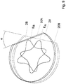
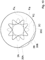
- all of the layers correspond to the plane of the ⁇ 001 ⁇ families, angularly offset from one another so as to homogenize the elastic and thermoelastic properties. In a preferred example, this offset angle between the corresponding crystal directions may be 30 degrees ( Figure 10 ).
- the height hs2 of the second layer of silicon Cs2 may be equal to or different from the sum of the heights hs1 and hs3 of the other two layers of silicon Cs1, Cs3.
- the sum of the heights of the separation layers Co1 and Co2 is advantageously at least 5%, preferably at least 10%, for example more than 20%, of the sum heights of the silicon layers Cs1, Cs2, Cs3.
- the thickness of the Co1, Co2 separation layers can advantageously be between 1 and 4 microns, for example 2 microns.
- Different separation layers can be made from the same material, or from different materials.
- the thickness of different separation layers can be the same or variable.
- Two layers of silicon can be separated by different separation layers made of different materials.
- At least one separating layer preferably has an isotropic Young's modulus and / or a thermal coefficient of the isotropic Young's modulus in its plane.
- the separating layer (s) therefore do not influence the isotropy of the Young's modulus of the resonator, in the planes parallel to the layers.
- the separation layers can be made from an amorphous material, for example amorphous SiO2.
- At least one separation layer may have a Young's modulus and / or a thermal coefficient of the Young's modulus anisotropic modulus in its plane, arranged to at least partially compensate for the residual anisotropy of the modulus. Young of stacked silicon layers, and / or the residual anisotropy of the second thermal coefficient of the Young's modulus.
- the resonator 1 may include an external layer, not illustrated, and made of a material having a thermal coefficient of the Young's modulus of sign opposite to that of silicon.
- the use of a separation layer performing thermal compensation between the first and second silicon layers makes it possible to limit the thickness of this outer layer, and therefore the manufacturing time of each resonator.
- the thickness of this outer layer can be greater than the thickness of the native silicon oxide resulting from the natural oxidation of silicon at room temperature.
- the sum of the areas of the separation layers and of the outer layer is determined so as to compensate as precisely as possible the variation of the Young's modulus depending on the temperature.
- the outer layer can be disposed on all the faces of the resonator, or only on the upper and lower faces. It can be obtained by oxidation of silicon in an oxidation chamber.
- the figure 10 illustrates a stack of three wafers of section plane ⁇ 001 ⁇ 2A, 2B and 2C.
- the crystal direction of the three wafers is shifted from each other.
- the offset is 30 °.
- Other offset values are possible.
- the figure also shows the value of the Young's modulus E A respectively E B and Ec, according to the direction, for each of the three wafers 2A, 2B and respectively 2C. As can be seen schematically in this figure, the value of the Young's modulus of the stack is homogenized according to the direction.
- multi-core resonators 1 are preferably etched in a stack of wafers sealed to one another before etching, at least one separation layer being produced on at least one of the wafers before their etching.
- the different wafers are therefore oriented with respect to each other before the resonators are etched.
- the figures 12 to 17 illustrate methods of making a resonator 1 according to figure 1 .
- the process of figure 12 uses two silicon wafers of the silicon on SOI type.
- Each silicon-on-insulator SOI type wafer comprises a substrate Su1, Su2 surmounted by an insulating layer Ci1, Ci2 then by a layer of monocrystalline silicon Cs1, Cs2.
- the substrate Su1, Su2, can be made of silicon.
- a separation layer Co1 for example an amorphous SiO2 layer, is deposited on the silicon layer Cs1 of the first wafer.
- one or more mechanical resonator patterns are etched on the separation layer Co1 and on the silicon layer Cs1.
- a third step 23 the silicon layer Cs2 of the second wafer is sealed on the separation layer Co1.
- the second wafer is offset by an angle ⁇ relative to the first wafer before this sealing step 23 so that the directions Ds1, Ds2 of the crystal lattices are also offset by an angle ⁇ .
- the assembly is turned over and the substrate Su1 as well as the insulating layer Ci1 of the first wafer are removed.
- the layer of silicon Cs2 of the second wafer is etched with the pattern of mechanical resonators using the first layer of silicon Cs1 as an etching mask. The etching can be performed by a deep reactive ion etching technique (also known by the acronym DRIE for "Deep Reactive Ion Etching").
- DRIE deep reactive ion etching technique
- the figure 13 illustrates a production method also using two SOI wafers.
- steps 32 and 33 two parts Cop1, Cop2 of the separation layer Co1 are respectively deposited on each silicon layer Cs1, Cs2 of the two SOI wafers.
- steps 34, 35 the patterns of the resonator (s) are then etched on the two parts Cop1 and Cop2 of the separation layer Co1 as well as on the two layers of silicon Cs1, Cs2 of the two wafers.
- the two parts Cop1, Cop2 are then sealed with an offset ⁇ between the wafers so as to form the complete separation layer Co1.
- Steps 37, 38 consist of removing the two substrates Su1, Su2 as well as the two insulating layers Ci1, Ci2 in order to free the mechanical resonator (s).
- the figure 14 illustrates a production method using a single wafer of the double-SOI type.
- a double-SOI type wafer consists of a substrate Su1 surmounted by a first layer of insulator Ci1, a first layer of monocrystalline silicon Cs1, a second layer of insulator Ci2 then a second layer of monocrystalline silicon Cs2.
- the second insulating layer Ci2 thus performs the function of the separation and thermal compensation layer Co1 of the resonator 1.
- the first layer of silicon Cs1 and the second layer of silicon Cs2 comprise crystal lattices whose directions are offset by an angle ⁇ .
- a first step 41 consists in etching the mechanical resonator pattern in the second layer of silicon Cs2, the second layer of insulator Cs2 and the first layer of silicon Cs1.
- a second step 42 consists in removing the substrate Su1 and the first insulating layer Ci1 to free the mechanical resonator.
- the figure 15 illustrates a variant of the figure 14 using a double-SOI type wafer.
- a first step 51 consists in etching the pattern of mechanical resonators in the second layer of silicon Cs2 and the second layer of insulator Cs2.
- a wafer of silicon Si2 is sealed on the second layer of silicon Cs2.
- This Si2 silicon wafer is a sacrificial layer which only serves as a support for the structure and will be removed in a later step.
- the assembly is turned over and the substrate Su1 as well as the first insulating layer Ci1 of the first wafer are removed.
- the mechanical resonator pattern is etched on the first silicon layer Cs1 in a step 54 and, in a step 55, the silicon wafer Si2 is removed to release the mechanical resonator (s) 1.
- This variant of the method of the figure 14 can be implemented when the resonators 1 are too thick and the etching step 41 does not allow the first silicon layer Cs1 to be correctly etched.
- the figure 16 illustrates a production process using an SOI type wafer and an Si2 silicon wafer.
- a separation layer Co1 is deposited on the silicon layer Cs1 of the first wafer of SOI type.
- a pattern of mechanical resonators is etched on the separation layer Co1 and on the silicon layer Cs1.
- the silicon wafer Si2 is then sealed with an offset ⁇ on the separation layer Co1 in a step 63.
- Step 64 consists in thinning the silicon wafer Si2 until the height hs2 desired for the second silicon layer Cs2 is reached. of resonator 1.
- a step 65 the pattern of mechanical resonator 1 is etched on the second silicon layer Cs2 formed by the silicon wafer Si2 and, in a step 66, the substrate Su1 and the insulating layer Ci1 are removed to release the mechanical resonator (s).
- the figure 17 illustrates a production method using a single wafer of the SOI type in which the substrate Su1 is made of silicon and forms the second layer of silicon Cs2.
- the separation layer Co1 is formed by an insulating layer Ci1 preferably made of silicon oxide.
- a first step 71 consists in thinning the substrate Su1 until the desired height hs2 is reached for the second layer of silicon Cs2.
- the pattern of one or more mechanical resonators is etched on the silicon layer Cs1.
- a structuring layer Cst is then deposited on the thinned substrate Su1 in a step 73 in order to stiffen the structure, then the pattern of mechanical resonators is etched in the layers of insulation Ci1 and of substrate Su1 in a step 74.
- the structuring layer Cst is removed to free the mechanical resonators 1.
- an external thermal compensation layer can be produced in a silicon oxidation chamber thus forming a layer of silicon oxide around resonator 1.
- the production of a second separation layer Co2 and a third layer of silicon Cs3 can be achieved, for example, by the sealing of a third silicon-on-insulator type wafer and by corresponding additional etching steps.
Landscapes
- Chemical & Material Sciences (AREA)
- Engineering & Computer Science (AREA)
- Metallurgy (AREA)
- Crystallography & Structural Chemistry (AREA)
- Materials Engineering (AREA)
- Organic Chemistry (AREA)
- Physics & Mathematics (AREA)
- General Physics & Mathematics (AREA)
- Manufacturing & Machinery (AREA)
- Micromachines (AREA)
- Piezo-Electric Or Mechanical Vibrators, Or Delay Or Filter Circuits (AREA)
Claims (16)
- Mechanischer Resonator, insbesondere für das Regulierorgan eines mechanischen Uhrwerks, wobei der Resonator folgendes umfasst:(i) eine erste Schicht aus Silizium (Csl), die aus einer ersten Kristallebene des Siliziums geschnitten wurde;(ii) eine zweite Schicht aus Silizium (Cs2), die aus einer zweiten Kristallebene des Siliziums geschnitten wurde;(iii) mindestens eine Trennschicht zwischen der ersten und zweiten Siliziumschicht (Cs1, Cs2);dadurch gekennzeichnet, dass
das Kristallgitter der ersten Schicht um einen Winkel gegenüber dem der zweiten Schicht verschoben ist, der weder 0°, noch 45° noch 180° beträgt und/oder dadurch, dass die erste Kristallebene anders ausgebildet ist als die zweite Kristallebene und mit ihr nicht übereinstimmt. - Resonator nach Anspruch 1, wobei mindestens eine der genannten Trennschichten aus einem amorphen Material besteht.
- Resonator nach einem der Ansprüche 1 oder 2, wobei mindestens eine der genannten Trennschichten in ihrer Ebene ein isotropes Young-Modul aufweist.
- Resonator nach einem der Ansprüche 1 bis 3, wobei mindestens eine der genannten Trennschichten einen Wärmekoeffizienten des isotropen Young-moduls in ihrer Ebene aufweist.
- Resonator nach Anspruch 1, wobei mindestens eine der genannten Trennschichten ein anisotropes Young-Modul und/oder einen thermischen Koeffizienten des anisotropen Young-Moduls in seiner Ebene aufweist, so angeordnet, um zumindest teilweise die Restanisotropie des Young-Moduls und/oder die Restanisotropie des zweiten thermischen Koeffizienten des Young-Moduls zu kompensieren.
- Resonator nach einem der Ansprüche 1 bis 5, wobei mindestens eine der genannten Trennschichten aus einem Material mit einem Wärmekoeffizienten des Young-Moduls mit entgegengesetztem Vorzeichen zu dem von Silizium besteht.
- Resonator nach einem der Ansprüche 1 bis 4, wobei mindestens eine der genannten Trennschichten aus SiO2 besteht.
- Ein Resonator nach einem der Ansprüche 1 bis 7, wobei die Dicke mindestens einer der genannten Trennschichten zwischen 1 und 4 Mikrometern beträgt.
- Resonator nach einem der Ansprüche 1 bis 8, wobei die zweite Kristallebene zur ersten Kristallebene verschieden ist und mit ihr nicht gleichwertig ist.
- Resonator nach einem der Ansprüche 1 bis 8, wobei die zweite Kristallebene mit der ersten Kristallebene identisch oder äquivalent ist, die Kristallrichtung der ersten Schicht um einen Winkel (a) gegenüber jeder äquivalenten Kristallrichtung der zweiten Schicht versetzt ist, der weder 0° noch 45° noch 90° beträgt, wodurch die Kristallgitterorientierungen der ersten und der zweiten Siliziumschicht unterschiedlich sind.
- Resonator nach einem der Ansprüche 1 bis 10, umfassend mehr als zwei Siliziumschichten, die durch mindestens eine Trennschicht voneinander getrennt sind.
- Resonator nach einem der Ansprüche 1 bis 11, umfassend eine Vielzahl der genannten Trennschichten zwischen den Siliziumschichten.
- Resonator nach einem der Ansprüche 1 bis 12, umfassend eine äußere Schicht, die aus einem Material mit einem thermischen Koeffizienten des Young-Moduls mit entgegengesetztem Vorzeichen zu dem von Silizium besteht.
- Verfahren zur Herstellung eines mechanischen Resonators nach einem der Ansprüche 1 bis 13, umfassend das Auftragen einer Trennschicht auf einem Siliziumwafer und das anschließende Ätzen einer Vielzahl von mechanischen Resonatoren in diesen Wafer.
- Verfahren nach Anspruch 14, umfassend das Auftragen einer zweiten Siliziumschicht auf der Trennschicht, wobei die mechanischen Resonatoren nach diesem Auftragen ausgeschnitten werden.
- Verfahren nach Anspruch 14, umfassend das Auftragen einer zweiten Siliziumschicht auf der Trennschicht nach dem genannten Ätzvorgang der mechanischen Resonatoren.
Priority Applications (1)
| Application Number | Priority Date | Filing Date | Title |
|---|---|---|---|
| EP16184620.9A EP3285124B1 (de) | 2016-08-17 | 2016-08-17 | Mechanischer resonator für uhrwerk, sowie herstellungsverfahren eines solchen resonators |
Applications Claiming Priority (1)
| Application Number | Priority Date | Filing Date | Title |
|---|---|---|---|
| EP16184620.9A EP3285124B1 (de) | 2016-08-17 | 2016-08-17 | Mechanischer resonator für uhrwerk, sowie herstellungsverfahren eines solchen resonators |
Publications (2)
| Publication Number | Publication Date |
|---|---|
| EP3285124A1 EP3285124A1 (de) | 2018-02-21 |
| EP3285124B1 true EP3285124B1 (de) | 2020-12-16 |
Family
ID=56738007
Family Applications (1)
| Application Number | Title | Priority Date | Filing Date |
|---|---|---|---|
| EP16184620.9A Active EP3285124B1 (de) | 2016-08-17 | 2016-08-17 | Mechanischer resonator für uhrwerk, sowie herstellungsverfahren eines solchen resonators |
Country Status (1)
| Country | Link |
|---|---|
| EP (1) | EP3285124B1 (de) |
Cited By (1)
| Publication number | Priority date | Publication date | Assignee | Title |
|---|---|---|---|---|
| WO2021053501A1 (fr) | 2019-09-16 | 2021-03-25 | Richemont International Sa | Procédé de fabrication d'une pluralité de résonateurs sur une plaquette |
Families Citing this family (1)
| Publication number | Priority date | Publication date | Assignee | Title |
|---|---|---|---|---|
| EP3839642A1 (de) * | 2019-12-20 | 2021-06-23 | Patek Philippe SA Genève | Herstellungsverfahren von uhrenfedern und ätzmaske für ein solches verfahren |
Citations (1)
| Publication number | Priority date | Publication date | Assignee | Title |
|---|---|---|---|---|
| EP3256910A1 (de) * | 2015-02-13 | 2017-12-20 | Tronic's Microsystems | Mechanischer oszillator und zugehöriges herstellungsverfahren |
Family Cites Families (9)
| Publication number | Priority date | Publication date | Assignee | Title |
|---|---|---|---|---|
| ATE307990T1 (de) | 2002-11-25 | 2005-11-15 | Suisse Electronique Microtech | Spiraluhrwerkfeder und verfahren zu deren herstellung |
| ATE416401T1 (de) | 2005-06-28 | 2008-12-15 | Eta Sa Mft Horlogere Suisse | Verstärktes mikromechanisches teil |
| DE602007013123D1 (de) | 2007-11-28 | 2011-04-21 | Manuf Et Fabrique De Montres Et De Chronometres Ulysse Nardin Le Locle S A | Mechanischer oszillator mit einem optimierten thermoelastischen koeffizienten |
| FR2925890B1 (fr) * | 2007-12-28 | 2010-01-29 | Commissariat Energie Atomique | Procede de fabrication de composants mecaniques de structures mems ou nems en silicium monocristallin |
| CH708067B1 (fr) * | 2008-10-22 | 2014-11-28 | Richemont Int Sa | Ressort spiral de montre autocompensé. |
| CH699780B1 (fr) | 2008-10-22 | 2014-02-14 | Richemont Int Sa | Ressort spiral de montre autocompensé. |
| DE102013114211B3 (de) * | 2013-07-22 | 2014-10-09 | Damasko Gmbh | Spiralfeder für mechanische Uhrwerke |
| WO2015087252A1 (de) * | 2013-12-11 | 2015-06-18 | Damasko Gmbh | Spiralfeder für mechanische uhrwerke |
| EP3088969B1 (de) * | 2016-03-17 | 2018-12-26 | Sigatec SA | Thermocompensierte spiralfeder und verfahren zu deren herstellung |
-
2016
- 2016-08-17 EP EP16184620.9A patent/EP3285124B1/de active Active
Patent Citations (1)
| Publication number | Priority date | Publication date | Assignee | Title |
|---|---|---|---|---|
| EP3256910A1 (de) * | 2015-02-13 | 2017-12-20 | Tronic's Microsystems | Mechanischer oszillator und zugehöriges herstellungsverfahren |
Cited By (1)
| Publication number | Priority date | Publication date | Assignee | Title |
|---|---|---|---|---|
| WO2021053501A1 (fr) | 2019-09-16 | 2021-03-25 | Richemont International Sa | Procédé de fabrication d'une pluralité de résonateurs sur une plaquette |
Also Published As
| Publication number | Publication date |
|---|---|
| EP3285124A1 (de) | 2018-02-21 |
Similar Documents
| Publication | Publication Date | Title |
|---|---|---|
| EP3256910B1 (de) | Mechanischer oszillator und zugehöriges herstellungsverfahren | |
| EP3181938B1 (de) | Herstellungsverfahren einer spiralfeder mit einer vorbestimmten steifigkeit durch wegnahme von material | |
| EP2514094B1 (de) | Thermokompensierter resonator mindestens ersten und zweiten grades | |
| EP2154583B1 (de) | Spiralfeder für Unruh-Spiralfeder | |
| EP3759554B1 (de) | Herstellungsverfahren einer spiralfeder | |
| WO2013064351A1 (fr) | Résonateur thermocompensé en céramique | |
| EP3100120A1 (de) | Wärmekompensierte spiralfeder aus keramik mit silicium in der zusammensetzung davon und verfahren zu anpassung davon | |
| CH707554A2 (fr) | Résonateur thermocompensé par un métal à mémoire de forme. | |
| CH713151B1 (fr) | Lame flexible pour l'horlogerie, et procédé de fabrication. | |
| WO2012152843A1 (fr) | Ressort spiral en silicium pour montre mecanique | |
| EP3769161B1 (de) | Herstellungsverfahren von thermokompensierten spiralen mit exakter steifigkeit | |
| CH702151A1 (fr) | Procede de realisation de pieces micromecaniques, notamment en verre ceramique. | |
| EP3285124B1 (de) | Mechanischer resonator für uhrwerk, sowie herstellungsverfahren eines solchen resonators | |
| EP3002638B1 (de) | Herstellungsverfahren einer thermokompensierten spiralfeder | |
| FR2924273A1 (fr) | Procede de moderation de deformation | |
| EP3047337B1 (de) | Mechanischer oszillator für uhrwerk und verfahren zur herstellung davon | |
| CH718081A2 (fr) | Élément élastique pour un système micromécanique. | |
| WO2016199039A1 (fr) | Résonateur horloger thermocompensé et méthode pour réaliser un tel résonateur | |
| CH712824A1 (fr) | Composant mécanique horloger ainsi que procédé de réalisation d'un tel composant. | |
| CH702353A2 (fr) | Résonateur thermocompensé au moins aux premier et second ordres. | |
| EP3907565A1 (de) | Verfahren zur herstellung einer uhrenkomponente aus silizium | |
| EP4121821A1 (de) | Verfahren zur herstellung eines uhrenbauteils auf siliziumbasis | |
| CH714705A2 (fr) | Ressort de rappel angulaire pour oscillateur thermo-compensé. | |
| CH711960B1 (fr) | Procédé de fabrication d'un spiral d'une raideur prédéterminée avec retrait de matière. | |
| CH710581A1 (fr) | Ressort spiral et son procédé de fabrication. |
Legal Events
| Date | Code | Title | Description |
|---|---|---|---|
| PUAI | Public reference made under article 153(3) epc to a published international application that has entered the european phase |
Free format text: ORIGINAL CODE: 0009012 |
|
| STAA | Information on the status of an ep patent application or granted ep patent |
Free format text: STATUS: THE APPLICATION HAS BEEN PUBLISHED |
|
| AK | Designated contracting states |
Kind code of ref document: A1 Designated state(s): AL AT BE BG CH CY CZ DE DK EE ES FI FR GB GR HR HU IE IS IT LI LT LU LV MC MK MT NL NO PL PT RO RS SE SI SK SM TR |
|
| AX | Request for extension of the european patent |
Extension state: BA ME |
|
| STAA | Information on the status of an ep patent application or granted ep patent |
Free format text: STATUS: REQUEST FOR EXAMINATION WAS MADE |
|
| 17P | Request for examination filed |
Effective date: 20180820 |
|
| RBV | Designated contracting states (corrected) |
Designated state(s): AL AT BE BG CH CY CZ DE DK EE ES FI FR GB GR HR HU IE IS IT LI LT LU LV MC MK MT NL NO PL PT RO RS SE SI SK SM TR |
|
| REG | Reference to a national code |
Ref country code: DE Ref legal event code: R079 Ref document number: 602016049770 Country of ref document: DE Free format text: PREVIOUS MAIN CLASS: G04B0017220000 Ipc: G04B0017280000 |
|
| GRAP | Despatch of communication of intention to grant a patent |
Free format text: ORIGINAL CODE: EPIDOSNIGR1 |
|
| STAA | Information on the status of an ep patent application or granted ep patent |
Free format text: STATUS: GRANT OF PATENT IS INTENDED |
|
| RIC1 | Information provided on ipc code assigned before grant |
Ipc: G04B 17/06 20060101ALI20200907BHEP Ipc: G04B 17/28 20060101AFI20200907BHEP Ipc: C30B 33/06 20060101ALI20200907BHEP Ipc: C30B 33/00 20060101ALI20200907BHEP Ipc: C30B 29/06 20060101ALI20200907BHEP Ipc: G04B 17/22 20060101ALI20200907BHEP |
|
| INTG | Intention to grant announced |
Effective date: 20201006 |
|
| GRAS | Grant fee paid |
Free format text: ORIGINAL CODE: EPIDOSNIGR3 |
|
| GRAA | (expected) grant |
Free format text: ORIGINAL CODE: 0009210 |
|
| STAA | Information on the status of an ep patent application or granted ep patent |
Free format text: STATUS: THE PATENT HAS BEEN GRANTED |
|
| RAP1 | Party data changed (applicant data changed or rights of an application transferred) |
Owner name: TRONIC'S MICROSYSTEMS S.A |
|
| AK | Designated contracting states |
Kind code of ref document: B1 Designated state(s): AL AT BE BG CH CY CZ DE DK EE ES FI FR GB GR HR HU IE IS IT LI LT LU LV MC MK MT NL NO PL PT RO RS SE SI SK SM TR |
|
| REG | Reference to a national code |
Ref country code: GB Ref legal event code: FG4D Free format text: NOT ENGLISH |
|
| REG | Reference to a national code |
Ref country code: IE Ref legal event code: FG4D Free format text: LANGUAGE OF EP DOCUMENT: FRENCH |
|
| REG | Reference to a national code |
Ref country code: DE Ref legal event code: R096 Ref document number: 602016049770 Country of ref document: DE |
|
| REG | Reference to a national code |
Ref country code: AT Ref legal event code: REF Ref document number: 1346153 Country of ref document: AT Kind code of ref document: T Effective date: 20210115 |
|
| PG25 | Lapsed in a contracting state [announced via postgrant information from national office to epo] |
Ref country code: RS Free format text: LAPSE BECAUSE OF FAILURE TO SUBMIT A TRANSLATION OF THE DESCRIPTION OR TO PAY THE FEE WITHIN THE PRESCRIBED TIME-LIMIT Effective date: 20201216 Ref country code: NO Free format text: LAPSE BECAUSE OF FAILURE TO SUBMIT A TRANSLATION OF THE DESCRIPTION OR TO PAY THE FEE WITHIN THE PRESCRIBED TIME-LIMIT Effective date: 20210316 Ref country code: GR Free format text: LAPSE BECAUSE OF FAILURE TO SUBMIT A TRANSLATION OF THE DESCRIPTION OR TO PAY THE FEE WITHIN THE PRESCRIBED TIME-LIMIT Effective date: 20210317 Ref country code: FI Free format text: LAPSE BECAUSE OF FAILURE TO SUBMIT A TRANSLATION OF THE DESCRIPTION OR TO PAY THE FEE WITHIN THE PRESCRIBED TIME-LIMIT Effective date: 20201216 |
|
| REG | Reference to a national code |
Ref country code: AT Ref legal event code: MK05 Ref document number: 1346153 Country of ref document: AT Kind code of ref document: T Effective date: 20201216 |
|
| REG | Reference to a national code |
Ref country code: NL Ref legal event code: MP Effective date: 20201216 |
|
| PG25 | Lapsed in a contracting state [announced via postgrant information from national office to epo] |
Ref country code: SE Free format text: LAPSE BECAUSE OF FAILURE TO SUBMIT A TRANSLATION OF THE DESCRIPTION OR TO PAY THE FEE WITHIN THE PRESCRIBED TIME-LIMIT Effective date: 20201216 Ref country code: LV Free format text: LAPSE BECAUSE OF FAILURE TO SUBMIT A TRANSLATION OF THE DESCRIPTION OR TO PAY THE FEE WITHIN THE PRESCRIBED TIME-LIMIT Effective date: 20201216 Ref country code: BG Free format text: LAPSE BECAUSE OF FAILURE TO SUBMIT A TRANSLATION OF THE DESCRIPTION OR TO PAY THE FEE WITHIN THE PRESCRIBED TIME-LIMIT Effective date: 20210316 |
|
| PG25 | Lapsed in a contracting state [announced via postgrant information from national office to epo] |
Ref country code: NL Free format text: LAPSE BECAUSE OF FAILURE TO SUBMIT A TRANSLATION OF THE DESCRIPTION OR TO PAY THE FEE WITHIN THE PRESCRIBED TIME-LIMIT Effective date: 20201216 Ref country code: HR Free format text: LAPSE BECAUSE OF FAILURE TO SUBMIT A TRANSLATION OF THE DESCRIPTION OR TO PAY THE FEE WITHIN THE PRESCRIBED TIME-LIMIT Effective date: 20201216 |
|
| REG | Reference to a national code |
Ref country code: LT Ref legal event code: MG9D |
|
| PG25 | Lapsed in a contracting state [announced via postgrant information from national office to epo] |
Ref country code: LT Free format text: LAPSE BECAUSE OF FAILURE TO SUBMIT A TRANSLATION OF THE DESCRIPTION OR TO PAY THE FEE WITHIN THE PRESCRIBED TIME-LIMIT Effective date: 20201216 Ref country code: SM Free format text: LAPSE BECAUSE OF FAILURE TO SUBMIT A TRANSLATION OF THE DESCRIPTION OR TO PAY THE FEE WITHIN THE PRESCRIBED TIME-LIMIT Effective date: 20201216 Ref country code: EE Free format text: LAPSE BECAUSE OF FAILURE TO SUBMIT A TRANSLATION OF THE DESCRIPTION OR TO PAY THE FEE WITHIN THE PRESCRIBED TIME-LIMIT Effective date: 20201216 Ref country code: CZ Free format text: LAPSE BECAUSE OF FAILURE TO SUBMIT A TRANSLATION OF THE DESCRIPTION OR TO PAY THE FEE WITHIN THE PRESCRIBED TIME-LIMIT Effective date: 20201216 Ref country code: RO Free format text: LAPSE BECAUSE OF FAILURE TO SUBMIT A TRANSLATION OF THE DESCRIPTION OR TO PAY THE FEE WITHIN THE PRESCRIBED TIME-LIMIT Effective date: 20201216 Ref country code: PT Free format text: LAPSE BECAUSE OF FAILURE TO SUBMIT A TRANSLATION OF THE DESCRIPTION OR TO PAY THE FEE WITHIN THE PRESCRIBED TIME-LIMIT Effective date: 20210416 Ref country code: SK Free format text: LAPSE BECAUSE OF FAILURE TO SUBMIT A TRANSLATION OF THE DESCRIPTION OR TO PAY THE FEE WITHIN THE PRESCRIBED TIME-LIMIT Effective date: 20201216 |
|
| PG25 | Lapsed in a contracting state [announced via postgrant information from national office to epo] |
Ref country code: AT Free format text: LAPSE BECAUSE OF FAILURE TO SUBMIT A TRANSLATION OF THE DESCRIPTION OR TO PAY THE FEE WITHIN THE PRESCRIBED TIME-LIMIT Effective date: 20201216 Ref country code: PL Free format text: LAPSE BECAUSE OF FAILURE TO SUBMIT A TRANSLATION OF THE DESCRIPTION OR TO PAY THE FEE WITHIN THE PRESCRIBED TIME-LIMIT Effective date: 20201216 |
|
| REG | Reference to a national code |
Ref country code: DE Ref legal event code: R097 Ref document number: 602016049770 Country of ref document: DE |
|
| PG25 | Lapsed in a contracting state [announced via postgrant information from national office to epo] |
Ref country code: IS Free format text: LAPSE BECAUSE OF FAILURE TO SUBMIT A TRANSLATION OF THE DESCRIPTION OR TO PAY THE FEE WITHIN THE PRESCRIBED TIME-LIMIT Effective date: 20210416 |
|
| PLBE | No opposition filed within time limit |
Free format text: ORIGINAL CODE: 0009261 |
|
| STAA | Information on the status of an ep patent application or granted ep patent |
Free format text: STATUS: NO OPPOSITION FILED WITHIN TIME LIMIT |
|
| PG25 | Lapsed in a contracting state [announced via postgrant information from national office to epo] |
Ref country code: IT Free format text: LAPSE BECAUSE OF FAILURE TO SUBMIT A TRANSLATION OF THE DESCRIPTION OR TO PAY THE FEE WITHIN THE PRESCRIBED TIME-LIMIT Effective date: 20201216 Ref country code: AL Free format text: LAPSE BECAUSE OF FAILURE TO SUBMIT A TRANSLATION OF THE DESCRIPTION OR TO PAY THE FEE WITHIN THE PRESCRIBED TIME-LIMIT Effective date: 20201216 |
|
| 26N | No opposition filed |
Effective date: 20210917 |
|
| PG25 | Lapsed in a contracting state [announced via postgrant information from national office to epo] |
Ref country code: DK Free format text: LAPSE BECAUSE OF FAILURE TO SUBMIT A TRANSLATION OF THE DESCRIPTION OR TO PAY THE FEE WITHIN THE PRESCRIBED TIME-LIMIT Effective date: 20201216 |
|
| PG25 | Lapsed in a contracting state [announced via postgrant information from national office to epo] |
Ref country code: ES Free format text: LAPSE BECAUSE OF FAILURE TO SUBMIT A TRANSLATION OF THE DESCRIPTION OR TO PAY THE FEE WITHIN THE PRESCRIBED TIME-LIMIT Effective date: 20201216 |
|
| PG25 | Lapsed in a contracting state [announced via postgrant information from national office to epo] |
Ref country code: SI Free format text: LAPSE BECAUSE OF FAILURE TO SUBMIT A TRANSLATION OF THE DESCRIPTION OR TO PAY THE FEE WITHIN THE PRESCRIBED TIME-LIMIT Effective date: 20201216 |
|
| REG | Reference to a national code |
Ref country code: DE Ref legal event code: R119 Ref document number: 602016049770 Country of ref document: DE |
|
| PG25 | Lapsed in a contracting state [announced via postgrant information from national office to epo] |
Ref country code: MC Free format text: LAPSE BECAUSE OF FAILURE TO SUBMIT A TRANSLATION OF THE DESCRIPTION OR TO PAY THE FEE WITHIN THE PRESCRIBED TIME-LIMIT Effective date: 20201216 |
|
| REG | Reference to a national code |
Ref country code: BE Ref legal event code: MM Effective date: 20210831 |
|
| GBPC | Gb: european patent ceased through non-payment of renewal fee |
Effective date: 20210817 |
|
| PG25 | Lapsed in a contracting state [announced via postgrant information from national office to epo] |
Ref country code: IS Free format text: LAPSE BECAUSE OF FAILURE TO SUBMIT A TRANSLATION OF THE DESCRIPTION OR TO PAY THE FEE WITHIN THE PRESCRIBED TIME-LIMIT Effective date: 20210416 Ref country code: LU Free format text: LAPSE BECAUSE OF NON-PAYMENT OF DUE FEES Effective date: 20210817 |
|
| PG25 | Lapsed in a contracting state [announced via postgrant information from national office to epo] |
Ref country code: IE Free format text: LAPSE BECAUSE OF NON-PAYMENT OF DUE FEES Effective date: 20210817 Ref country code: GB Free format text: LAPSE BECAUSE OF NON-PAYMENT OF DUE FEES Effective date: 20210817 Ref country code: DE Free format text: LAPSE BECAUSE OF NON-PAYMENT OF DUE FEES Effective date: 20220301 Ref country code: BE Free format text: LAPSE BECAUSE OF NON-PAYMENT OF DUE FEES Effective date: 20210831 |
|
| PG25 | Lapsed in a contracting state [announced via postgrant information from national office to epo] |
Ref country code: HU Free format text: LAPSE BECAUSE OF FAILURE TO SUBMIT A TRANSLATION OF THE DESCRIPTION OR TO PAY THE FEE WITHIN THE PRESCRIBED TIME-LIMIT; INVALID AB INITIO Effective date: 20160817 |
|
| PG25 | Lapsed in a contracting state [announced via postgrant information from national office to epo] |
Ref country code: CY Free format text: LAPSE BECAUSE OF FAILURE TO SUBMIT A TRANSLATION OF THE DESCRIPTION OR TO PAY THE FEE WITHIN THE PRESCRIBED TIME-LIMIT Effective date: 20201216 |
|
| PGFP | Annual fee paid to national office [announced via postgrant information from national office to epo] |
Ref country code: CH Payment date: 20230902 Year of fee payment: 8 |
|
| PGFP | Annual fee paid to national office [announced via postgrant information from national office to epo] |
Ref country code: FR Payment date: 20230828 Year of fee payment: 8 |
|
| PG25 | Lapsed in a contracting state [announced via postgrant information from national office to epo] |
Ref country code: MK Free format text: LAPSE BECAUSE OF FAILURE TO SUBMIT A TRANSLATION OF THE DESCRIPTION OR TO PAY THE FEE WITHIN THE PRESCRIBED TIME-LIMIT Effective date: 20201216 |