EP3285124B1 - Mechanical resonator for timepiece and method for manufacturing such a resonator - Google Patents
Mechanical resonator for timepiece and method for manufacturing such a resonator Download PDFInfo
- Publication number
- EP3285124B1 EP3285124B1 EP16184620.9A EP16184620A EP3285124B1 EP 3285124 B1 EP3285124 B1 EP 3285124B1 EP 16184620 A EP16184620 A EP 16184620A EP 3285124 B1 EP3285124 B1 EP 3285124B1
- Authority
- EP
- European Patent Office
- Prior art keywords
- silicon
- layer
- young
- modulus
- resonator
- Prior art date
- Legal status (The legal status is an assumption and is not a legal conclusion. Google has not performed a legal analysis and makes no representation as to the accuracy of the status listed.)
- Active
Links
- 238000004519 manufacturing process Methods 0.000 title claims description 21
- 238000000034 method Methods 0.000 title claims description 17
- XUIMIQQOPSSXEZ-UHFFFAOYSA-N Silicon Chemical compound [Si] XUIMIQQOPSSXEZ-UHFFFAOYSA-N 0.000 claims description 150
- 229910052710 silicon Inorganic materials 0.000 claims description 135
- 239000010703 silicon Substances 0.000 claims description 135
- 238000000926 separation method Methods 0.000 claims description 60
- 239000013078 crystal Substances 0.000 claims description 56
- VYPSYNLAJGMNEJ-UHFFFAOYSA-N Silicium dioxide Chemical compound O=[Si]=O VYPSYNLAJGMNEJ-UHFFFAOYSA-N 0.000 claims description 35
- 239000000463 material Substances 0.000 claims description 24
- 238000005530 etching Methods 0.000 claims description 20
- 229910052681 coesite Inorganic materials 0.000 claims description 14
- 229910052906 cristobalite Inorganic materials 0.000 claims description 14
- 239000000377 silicon dioxide Substances 0.000 claims description 14
- 229910052682 stishovite Inorganic materials 0.000 claims description 14
- 229910052905 tridymite Inorganic materials 0.000 claims description 14
- 238000000151 deposition Methods 0.000 claims description 10
- 230000008021 deposition Effects 0.000 claims description 6
- 230000001105 regulatory effect Effects 0.000 claims description 5
- 235000012431 wafers Nutrition 0.000 description 87
- 235000012239 silicon dioxide Nutrition 0.000 description 13
- 239000000758 substrate Substances 0.000 description 13
- 229910021421 monocrystalline silicon Inorganic materials 0.000 description 11
- 230000003647 oxidation Effects 0.000 description 10
- 238000007254 oxidation reaction Methods 0.000 description 10
- 229910052814 silicon oxide Inorganic materials 0.000 description 7
- 239000012212 insulator Substances 0.000 description 6
- 230000018109 developmental process Effects 0.000 description 5
- 230000010355 oscillation Effects 0.000 description 5
- 230000010363 phase shift Effects 0.000 description 5
- 238000007789 sealing Methods 0.000 description 5
- PEDCQBHIVMGVHV-UHFFFAOYSA-N Glycerine Chemical compound OCC(O)CO PEDCQBHIVMGVHV-UHFFFAOYSA-N 0.000 description 4
- 238000000708 deep reactive-ion etching Methods 0.000 description 4
- 101100273635 Rattus norvegicus Ccn5 gene Proteins 0.000 description 3
- 229910021486 amorphous silicon dioxide Inorganic materials 0.000 description 3
- 229910021419 crystalline silicon Inorganic materials 0.000 description 3
- 230000001902 propagating effect Effects 0.000 description 3
- 230000029058 respiratory gaseous exchange Effects 0.000 description 3
- 241000397921 Turbellaria Species 0.000 description 2
- 238000005452 bending Methods 0.000 description 2
- 230000007547 defect Effects 0.000 description 2
- 230000000694 effects Effects 0.000 description 2
- 230000001747 exhibiting effect Effects 0.000 description 2
- 230000002093 peripheral effect Effects 0.000 description 2
- 238000007493 shaping process Methods 0.000 description 2
- 239000013598 vector Substances 0.000 description 2
- 229910000942 Elinvar Inorganic materials 0.000 description 1
- 240000008042 Zea mays Species 0.000 description 1
- 239000002131 composite material Substances 0.000 description 1
- 230000001276 controlling effect Effects 0.000 description 1
- 238000005336 cracking Methods 0.000 description 1
- 238000005520 cutting process Methods 0.000 description 1
- 230000001419 dependent effect Effects 0.000 description 1
- 230000012447 hatching Effects 0.000 description 1
- 238000010438 heat treatment Methods 0.000 description 1
- 238000009413 insulation Methods 0.000 description 1
- 238000005304 joining Methods 0.000 description 1
- 239000002184 metal Substances 0.000 description 1
- 239000005300 metallic glass Substances 0.000 description 1
- 239000000203 mixture Substances 0.000 description 1
- 238000000206 photolithography Methods 0.000 description 1
- 230000021715 photosynthesis, light harvesting Effects 0.000 description 1
- 230000002028 premature Effects 0.000 description 1
- 238000009877 rendering Methods 0.000 description 1
- 230000035945 sensitivity Effects 0.000 description 1
- 238000004088 simulation Methods 0.000 description 1
- 230000009466 transformation Effects 0.000 description 1
- 238000009279 wet oxidation reaction Methods 0.000 description 1
Images


Classifications
-
- G—PHYSICS
- G04—HOROLOGY
- G04B—MECHANICALLY-DRIVEN CLOCKS OR WATCHES; MECHANICAL PARTS OF CLOCKS OR WATCHES IN GENERAL; TIME PIECES USING THE POSITION OF THE SUN, MOON OR STARS
- G04B17/00—Mechanisms for stabilising frequency
- G04B17/04—Oscillators acting by spring tension
- G04B17/06—Oscillators with hairsprings, e.g. balance
- G04B17/066—Manufacture of the spiral spring
-
- C—CHEMISTRY; METALLURGY
- C30—CRYSTAL GROWTH
- C30B—SINGLE-CRYSTAL GROWTH; UNIDIRECTIONAL SOLIDIFICATION OF EUTECTIC MATERIAL OR UNIDIRECTIONAL DEMIXING OF EUTECTOID MATERIAL; REFINING BY ZONE-MELTING OF MATERIAL; PRODUCTION OF A HOMOGENEOUS POLYCRYSTALLINE MATERIAL WITH DEFINED STRUCTURE; SINGLE CRYSTALS OR HOMOGENEOUS POLYCRYSTALLINE MATERIAL WITH DEFINED STRUCTURE; AFTER-TREATMENT OF SINGLE CRYSTALS OR A HOMOGENEOUS POLYCRYSTALLINE MATERIAL WITH DEFINED STRUCTURE; APPARATUS THEREFOR
- C30B29/00—Single crystals or homogeneous polycrystalline material with defined structure characterised by the material or by their shape
- C30B29/02—Elements
- C30B29/06—Silicon
-
- C—CHEMISTRY; METALLURGY
- C30—CRYSTAL GROWTH
- C30B—SINGLE-CRYSTAL GROWTH; UNIDIRECTIONAL SOLIDIFICATION OF EUTECTIC MATERIAL OR UNIDIRECTIONAL DEMIXING OF EUTECTOID MATERIAL; REFINING BY ZONE-MELTING OF MATERIAL; PRODUCTION OF A HOMOGENEOUS POLYCRYSTALLINE MATERIAL WITH DEFINED STRUCTURE; SINGLE CRYSTALS OR HOMOGENEOUS POLYCRYSTALLINE MATERIAL WITH DEFINED STRUCTURE; AFTER-TREATMENT OF SINGLE CRYSTALS OR A HOMOGENEOUS POLYCRYSTALLINE MATERIAL WITH DEFINED STRUCTURE; APPARATUS THEREFOR
- C30B33/00—After-treatment of single crystals or homogeneous polycrystalline material with defined structure
- C30B33/005—Oxydation
-
- C—CHEMISTRY; METALLURGY
- C30—CRYSTAL GROWTH
- C30B—SINGLE-CRYSTAL GROWTH; UNIDIRECTIONAL SOLIDIFICATION OF EUTECTIC MATERIAL OR UNIDIRECTIONAL DEMIXING OF EUTECTOID MATERIAL; REFINING BY ZONE-MELTING OF MATERIAL; PRODUCTION OF A HOMOGENEOUS POLYCRYSTALLINE MATERIAL WITH DEFINED STRUCTURE; SINGLE CRYSTALS OR HOMOGENEOUS POLYCRYSTALLINE MATERIAL WITH DEFINED STRUCTURE; AFTER-TREATMENT OF SINGLE CRYSTALS OR A HOMOGENEOUS POLYCRYSTALLINE MATERIAL WITH DEFINED STRUCTURE; APPARATUS THEREFOR
- C30B33/00—After-treatment of single crystals or homogeneous polycrystalline material with defined structure
- C30B33/06—Joining of crystals
-
- G—PHYSICS
- G04—HOROLOGY
- G04B—MECHANICALLY-DRIVEN CLOCKS OR WATCHES; MECHANICAL PARTS OF CLOCKS OR WATCHES IN GENERAL; TIME PIECES USING THE POSITION OF THE SUN, MOON OR STARS
- G04B17/00—Mechanisms for stabilising frequency
- G04B17/20—Compensation of mechanisms for stabilising frequency
- G04B17/22—Compensation of mechanisms for stabilising frequency for the effect of variations of temperature
- G04B17/227—Compensation of mechanisms for stabilising frequency for the effect of variations of temperature composition and manufacture of the material used
-
- G—PHYSICS
- G04—HOROLOGY
- G04B—MECHANICALLY-DRIVEN CLOCKS OR WATCHES; MECHANICAL PARTS OF CLOCKS OR WATCHES IN GENERAL; TIME PIECES USING THE POSITION OF THE SUN, MOON OR STARS
- G04B17/00—Mechanisms for stabilising frequency
- G04B17/20—Compensation of mechanisms for stabilising frequency
- G04B17/28—Compensation of mechanisms for stabilising frequency for the effect of unbalance of the weights, e.g. tourbillon
Definitions
- the invention relates to a mechanical resonator intended to equip a regulating member of a timepiece and to a method of manufacturing such a resonator.
- the invention finds a particularly advantageous application for resonators with radial symmetry oscillating in “breathing mode”. More specifically, the invention finds a particularly advantageous application for balance springs intended to equip the balance of a mechanical timepiece assembly such as a watch.
- the movements of mechanical watches are regulated by means of a mechanical regulator comprising a resonator, that is to say an elastically deformable component whose oscillations determine the rate of the watch.
- a mechanical regulator comprising a resonator, that is to say an elastically deformable component whose oscillations determine the rate of the watch.
- Many watches include, for example, a regulator comprising a hairspring as resonator, mounted on the axis of a balance and set in oscillation by means of an escapement; the natural frequency of the balance-spring pair makes it possible to regulate the watch.
- Other known types of resonators are based, for example, on tuning forks, oscillating bars, or other mechanical elements.
- the natural resonant frequency of the balance spring is proportional to the square root of its stiffness. Consequently, the frequency of the hairspring is proportional to the square root of the Young's modulus of the material. So, if the Young's modulus varies as a function of temperature, the frequency of the hairspring will also vary as a function of temperature. For a weak variation in temperature, the frequency of the hairspring therefore depends in the first order on the variation in temperature of the Young's modulus.
- Silicon has a very negative first thermoelastic coefficient value, close to -64 ppm / C. Consequently, the stiffness of a silicon resonator, and therefore its natural frequency, varies greatly with temperature. A pure silicon mechanical resonator is therefore anisochronous.
- EP1422436 suggests a spiral-type mechanical resonator made from a monocrystalline silicon core and whose variations in temperature of the Young's modulus are compensated for by a layer surrounding the core and made from a material having a first thermoelastic coefficient of opposite sign to that of silicon.
- the outer layer is made of amorphous SiO2, one of the rare materials exhibiting a positive thermoelastic coefficient (+213 ppm / C).
- EP1422436 suggests a silicon balance spring obtained from a wafer cut along the ⁇ 001 ⁇ crystal plane.
- the figure 11A illustrates this plane, and two equivalent planes ⁇ 010 ⁇ and ⁇ 100 ⁇ , in the case of a crystal with a cubic face.
- the silicon network has a centered cubic face and therefore has six additional nodes in the center of each of the faces of this cube, which are not represented on the figures 11A to 11C for the simplification of the figure; the definition of the crystalline planes is however identical.
- the ⁇ 001 ⁇ section exhibits a relatively high planar anisotropy factor.
- the situation is illustrated on the figure 2 which shows the value of Young's modulus E (flexural stiffness) in different directions in the plane of the hairspring, as well as the average value E (average) of this modulus (about 148 GPa)
- the anisotropy of the planar Young's modulus of a resonator etched in a wafer cut along the ⁇ 001 ⁇ plane is also troublesome if one wants to correctly control the equivalent stiffness of a resonator of complex shape during its design phase . Indeed, to obtain a good correlation between the calculated values and the measured values for the equivalent stiffness, one must take into account in particular the precise orientation of the elements of the resonator which do not exhibit a perfectly radial symmetry with respect to the various planar directions of the wafer.
- EP2215531 suggests a silicon balance-spring covered with a thermal compensation layer but whose core is obtained from a wafer cut in the ⁇ 111 ⁇ plane, illustrated on figure 11C in the case of a cubic network.
- the figure 3 shows that the Young modulus E is almost isotropic in this plane; its mean value E (mean) is about 169 GPa.
- a resonator with radial symmetry which oscillates in breathing mode such as for example a hairspring, made in a wafer cut in the ⁇ 111 ⁇ plane will have a more concentric development than a resonator of the same type made in a wafer cut in the plane ⁇ 001 ⁇ or ⁇ 110 ⁇ .
- the process of shaping the silicon of orientation ⁇ 111> is however more delicate than that used on wafers of orientations ⁇ 001> ⁇
- the anisotropy of the silicon crystal influences to a lesser extent the temperature sensitivity of the Young's modulus.
- the first thermal coefficient that is to say the derivative dE / dT of the Young modulus compared to the temperature, is certainly isotropic whatever the crystalline plane of the section ⁇ 110 ⁇ , ⁇ 111 ⁇ or ⁇ 001 ⁇ ( Figure 5 ).
- the value of the first thermal coefficient for the sections according to the plans ⁇ 110 ⁇ , ⁇ 111 ⁇ is -64.25 ppm / C and -64.27 ppm / C for the plane ⁇ 001 ⁇ .
- thermoelastic coefficients of order greater than "1" is advantageous in particular in the control of the thermocompensation of resonators with medium or low radial symmetry needing to be thermocompensated from the second order.
- the growth of an oxide layer on the balance spring EP2215531 is obtained by a wet oxidation process. Oxidation of balance springs by heating in a dry oxidation chamber has also been suggested. In any case, the growth of the oxide is a slow process, which leads to a long manufacturing cycle time.
- SiO2 For the typical dimensions of balance springs for mechanical watches, it is necessary to grow on the surface of the silicon relatively thick layers of SiO2, between 2 and 5 microns, in order to thermocompensate the balance-spring-balance assembly. It is known that from a certain thickness of thermal SiO2 (approx. 3 ⁇ m) the physicochemical properties of these layers degrade and their growth becomes too slow. For example, the growth of 3 microns of SiO2 thermally lasts more than 50 hours.
- Silicon is a brittle material with flexural breaking stresses of less than 10 GPa and fatigue stresses of the order of 2 to 3 GPa.
- the presence of sharp angles in the typical structures of a silicon resonator is the cause of high stress concentrations, which can rapidly produce deformations and accelerate failure.
- EP1904901 describes the advantages of a layer of SiO2 on the surface of a watch component produced in a wafer (or wafer) of monocrystalline silicon in order to reinforce its mechanical resistance. Despite this protection, any crack or defect capable of propagating beyond the oxidized surface of this component will eventually cause its total breakage as it will propagate unhindered through the crystal structure of the component.
- the growth of an oxide layer on the surface of a silicon hairspring takes place at high temperature, typically at 1100 ° C.
- the original dimensions of the silicon component expand under the effect of heat and in proportion to the coefficient of thermal expansion ⁇ Si .
- the growth of the oxide therefore takes place on a component with dimensions dilated.
- the return to ambient temperature at the end of the process takes place on a composite component, formed of a silicon core and the newly formed peripheral oxide layer.
- the coefficient of thermal expansion of silicon oxide being ⁇ SiO2 different from that of silicon ⁇ Si ( ⁇ Si > ⁇ SiO2 ), there follows a residual elongation of the dimensions and a stressing of the component.
- CH699780 presents a spiral-type mechanical resonator made from a monocrystalline silicon wafer.
- the variations in temperature of the Young's modulus of the hairspring are compensated for by two amorphous metal layers or oxide layers arranged inside the silicon bar and whose thermal coefficient of the Young's modulus is opposite to that of silicon. This solution does not make it possible to compensate for the anisotropy of the Young's modulus in the plane of the hairspring.
- An object of the present invention is to provide a mechanical resonator, in particular for the regulating member of a mechanical clockwork movement, which makes it possible to avoid the above drawbacks, or in any case to offer a better compromise between these disadvantages.
- an aim of the present invention is to provide a new mechanical resonator.
- an aim of the present invention is to provide a thermocompensated mechanical resonator.
- Another aim is to provide a mechanical resonator that is less fragile than resonators made of silicon or of silicon oxidized at the surface.
- Another aim is to provide a mechanical resonator whose development is concentric.
- Another aim is to provide a mechanical resonator whose development concentricity is little affected by temperature.
- Another aim is to provide a mechanical resonator that is faster to produce.
- An aim is also to overcome the drawbacks mentioned above and therefore to propose a mechanical oscillator in monocrystalline silicon, simple to manufacture, the mechanical characteristics of which are similar in all directions of a plane.
- Another aim is to provide a mechanical resonator with more precise dimensions and exhibiting fewer residual stresses.
- a silicon layer is said to be cut along a given crystalline plane of silicon if it has been obtained by etching a wafer cut along this plane.
- Crystal lattices are shifted by an angle ⁇ when the corresponding or equivalent crystal directions are shifted by an angle ⁇ .
- crystal directions (or nodal directions) of the layers correspond to the directions of the vectors [xyz] joining the nodes n of the crystal. Since silicon has a crystal structure with cubic symmetry, the four diagonals are equivalent, the three faces of the cube are equivalent, etc.
- the directions [100], [1 - 00], [010], [01 - 0], [001], [001] and [001 - ] are equivalent to each other and designated by a family of directions ⁇ 100 > (the operator - designating the opposition).
- Planes are said to be equivalent if they can be obtained by permutations and / or oppositions of the indices.
- the plane (xyz) is perpendicular to the direction [xyz].
- the planes (100), (1 - 00), (010), (01 - 0), (001), (001) and (001 - ) are equivalent and form a family of planes designated by ⁇ 100 ⁇ (the operator - designating the opposition).
- the resonator does not consist of a monocrystalline and monolithic structure but of several monocrystalline layers of crystal lattices separated from one another by one or more separation layers.
- a crack generated in one crystalline silicon layer can be stopped by the separating layer, and avoid propagating to the other crystalline layer.
- the mechanical robustness is enhanced.
- a crack generated in a layer of crystalline silicon and which would have passed through the separation layer or layers has less risk of propagating into the other layer of crystalline silicon, due to the phase shifts between the cracking planes.
- the mechanical robustness is also reinforced thanks to the etching of the different layers of silicon of the resonator in different and non-equivalent crystalline planes.
- the first silicon layer can be etched in a wafer cut along the ⁇ 001 ⁇ plane and the second silicon layer in a wafer cut along the ⁇ 011 ⁇ plane or along the ⁇ 111 ⁇ plane.
- the first silicon layer can be etched in a wafer cut along the ⁇ 011 ⁇ plane and the second silicon layer in a wafer etched along the ⁇ 111 ⁇ plane.
- the crystal orientations are essentially different and there is intrinsically an angular offset of the respective networks which favors the robustness of the structure.
- At least one release layer can be made of an amorphous material. Amorphous material further reduces the risk of crack propagation.
- the latter has a Young's modulus which is also isotropic.
- This separation layer therefore homogeneously compensates for the variations in stiffness undergone by the resonator, and does not add undesirable anisotropy.
- At least one separation layer preferably has a first thermal coefficient of the isotropic Young's modulus in the plane of the layer.
- At least one separation layer preferably has a second thermal coefficient of the Young's modulus isotropic in the plane of the layer.
- At least one separating layer has a Young's modulus, or a second thermal coefficient of the Young's modulus, anisotropic in its plane.
- the separation layer is then preferably oriented relative to the silicon layers so that it compensates for the residual anisotropy of the Young's modulus, and / or the residual anisotropy of the second thermal coefficient of the Young's modulus.
- At least one separating layer can be made of a material having a thermal coefficient of Young's modulus of sign opposite to that of silicon.
- the thermocompensation of the mechanical resonator does not take place, or not only, by means of an outer SiO2 layer but also by means of at least one buried separation layer.
- At least one separation layer can consist of SiO2.
- the oxidation of devices using this type of element, such as flexible guides, is very limited.
- the resonator can include more than two layers of silicon separated from each other.
- the resonator can comprise several separation layers between two layers of silicon.
- the resonator may include an outer layer made of a material having a thermal coefficient of the Young's modulus of sign opposite to that of silicon.
- the use of the separating layer performing thermal compensation between the first and second silicon layers makes it possible to limit the thickness of this outer layer.
- the thickness of this outer layer is greater than the thickness of the native silicon oxide resulting from the natural oxidation of silicon at room temperature.
- the resonator can be a radially symmetrical mechanical resonator.
- the resonator can be a mechanical resonator of the spiral type.
- the subject of the invention is also a method of manufacturing a mechanical resonator.
- the method of manufacturing a mechanical resonator comprises the deposition of a separation layer on a silicon wafer, then the etching of several mechanical resonators in this wafer.
- the separation layer may for example be a thermal compensation layer, for example a layer of SiO2.
- the thermal compensation layer is thus deposited in a single operation on all the resonators produced from a wafer, which reduces the manufacturing time and the risk of breaking the resonators during their handling after their etching.
- the term “depositing a layer of material” is understood to mean the processes consisting in adding material by deposition, adding material by growth and transformation of the existing material or the transfer of an additional layer by sealing of the annex layer.
- the method may include the deposition of a second layer of silicon on the separation layer, the mechanical resonators being etched after this deposition.
- the method may include the deposition of a second layer of silicon on the separation layer after said step of etching the mechanical resonators.
- the first layer of silicon can then be used as a mask for etching the second layer of silicon.
- the method may include the sealing of several silicon wafers, at least one of which is covered with a separation layer, for example a layer of SiO2, then the etching of a plurality of resonators in this stack.
- a separation layer for example a layer of SiO2
- the figure 7 illustrates a cross section of a portion of a mechanical resonator, for example in the form of a straight segment, a helicoid or a spiral spiral.
- This figure shows a stack of three layers: a first layer of monocrystalline silicon Cs1 directly in contact with a separation layer Co1 directly in contact with a second layer of monocrystalline Cs2 silicon.
- the Co1 separation layer can be a thermal compensation layer, for example a layer of amorphous material, for example a layer of SiO2.
- the first layer of silicon Cs1 extends over a height hs1 and over the entire width L of the resonator 1.
- the second layer of silicon Cs2 extends over a height hs2 substantially equal to the height hs1 and over the entire width L.
- separation layer Co1 extends over a height ho1 much less than the two heights hs1, hs2 and over the entire width L.
- the first layer of silicon Cs1 and the second layer of silicon come from wafers cut along the same crystal plane, preferably the ⁇ 001 ⁇ plane, or the ⁇ 011 ⁇ plane. It is also possible to provide a stack of silicon layers obtained from wafers cut along different crystal planes; for example a layer cut from a wafer ⁇ 001 ⁇ and another layer cut from a wafer ⁇ 011 ⁇ .
- the crystal lattice Ds1 of the first layer of silicon Cs1 is offset by an angle ⁇ with respect to the crystal lattice Ds2 of the second layer of silicon Cs2.
- the directions Ds1, Ds2 are defined from any corresponding crystal vector in the layers Cs1, Cs2.
- the separation layer Co1 is advantageously made of a material having a thermal coefficient of the Young's modulus of sign opposite to that of silicon so that the variation in the stiffness of the silicon layers Cs1, Cs2 as a function of the temperature is, at least partially, compensated by the separation layer Co1.
- the Co1 separation layer is formed of silicon oxide.
- the thermal coefficient of the Young's modulus for silicon is -64.10 -6 K -1 and the thermal coefficient of Young's modulus for silicon oxide is 187.5.10 -6 K -1 at room temperature, approximately 20 ° C.
- the volume ratio between the separation and thermal compensation layer Co1 and the silicon layers Cs1, Cs2 is advantageously at least 5%, preferably at least 10%, for example more than 20%, at an ambient temperature of 20 ° C.
- the area of the section ho1.L is therefore at least equal to 20% of the area of the sections L.hs1 and L.hs2.
- the thickness of the Co1 separation layer is between 1 and 4 microns, for example 2 microns.
- the figure 9 illustrates a stack of two wafers cut in the ⁇ 001 ⁇ plane, the crystal lattice of the upper wafer 2B being angularly offset by an angle ⁇ in this example with respect to the crystal lattice of the lower wafer 2A.
- the figure also shows the value of the Young's modulus E A respectively E B , according to the direction, for each of the two wafers 2A respectively 2B.
- the maxima and minima of the Young modulus do not correspond on the two wafers, so that the value of the Young modulus of the two superimposed wafers (or of a component engraved in these two superimposed wafers) is less dependent on the direction.
- the phase shift ⁇ is 30 °.
- other phase shift values are possible, for example any value other than NX 90 °, N being any integer.
- the phase shift is also different from 45 °.
- phase shift of the superimposed wafers can be obtained by controlling the angle between these two flats, then by sealing the two wafers to each other before etching the resonators.
- the figure 8 illustrates a variant of the invention in which the resonator 1, illustrated in cross section, comprises three layers of silicon Cs1, Cs2, Cs3 interspersed by two thermal compensation layers Co1, Co2.
- the crystal direction Ds1 of the first layer of silicon Cs1 is the same as the crystal direction Ds3 of the third layer of silicon Cs3.
- the second layer of silicon Cs2 disposed between the first and the third layer of silicon Cs1, Cs3 comprises a crystal lattice whose direction Ds2 is offset by an angle preferably different from 0 °, 45 ° and 180 ° with respect to the crystal directions corresponding layers Ds1, Ds3.
- the first layer of silicon Cs1 and the third layer of silicon are etched in wafers cut along the same crystal plane, preferably the ⁇ 001 ⁇ plane, or of the ⁇ 011 ⁇ family.
- the second silicon layer is for its part etched in a wafer along the ⁇ 111 ⁇ crystal plane which has more homogeneous thermoelastic properties in all directions of the plane. The compensation of the variations of the Young's modulus according to the direction is thus done above all between the layers Cs1 and Cs3.
- the layers Cs1 to Cs3 can however correspond to any section plane or combination of section planes of the plan families ⁇ 110 ⁇ , ⁇ 111 ⁇ and ⁇ 001 ⁇ .
- the layers correspond to a combination of the section planes of the ⁇ 110 ⁇ and ⁇ 001 ⁇ families.
- all of the layers correspond to the plane of the ⁇ 001 ⁇ families, angularly offset from one another so as to homogenize the elastic and thermoelastic properties. In a preferred example, this offset angle between the corresponding crystal directions may be 30 degrees ( Figure 10 ).
- the height hs2 of the second layer of silicon Cs2 may be equal to or different from the sum of the heights hs1 and hs3 of the other two layers of silicon Cs1, Cs3.
- the sum of the heights of the separation layers Co1 and Co2 is advantageously at least 5%, preferably at least 10%, for example more than 20%, of the sum heights of the silicon layers Cs1, Cs2, Cs3.
- the thickness of the Co1, Co2 separation layers can advantageously be between 1 and 4 microns, for example 2 microns.
- Different separation layers can be made from the same material, or from different materials.
- the thickness of different separation layers can be the same or variable.
- Two layers of silicon can be separated by different separation layers made of different materials.
- At least one separating layer preferably has an isotropic Young's modulus and / or a thermal coefficient of the isotropic Young's modulus in its plane.
- the separating layer (s) therefore do not influence the isotropy of the Young's modulus of the resonator, in the planes parallel to the layers.
- the separation layers can be made from an amorphous material, for example amorphous SiO2.
- At least one separation layer may have a Young's modulus and / or a thermal coefficient of the Young's modulus anisotropic modulus in its plane, arranged to at least partially compensate for the residual anisotropy of the modulus. Young of stacked silicon layers, and / or the residual anisotropy of the second thermal coefficient of the Young's modulus.
- the resonator 1 may include an external layer, not illustrated, and made of a material having a thermal coefficient of the Young's modulus of sign opposite to that of silicon.
- the use of a separation layer performing thermal compensation between the first and second silicon layers makes it possible to limit the thickness of this outer layer, and therefore the manufacturing time of each resonator.
- the thickness of this outer layer can be greater than the thickness of the native silicon oxide resulting from the natural oxidation of silicon at room temperature.
- the sum of the areas of the separation layers and of the outer layer is determined so as to compensate as precisely as possible the variation of the Young's modulus depending on the temperature.
- the outer layer can be disposed on all the faces of the resonator, or only on the upper and lower faces. It can be obtained by oxidation of silicon in an oxidation chamber.
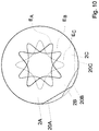
- the figure 10 illustrates a stack of three wafers of section plane ⁇ 001 ⁇ 2A, 2B and 2C.
- the crystal direction of the three wafers is shifted from each other.
- the offset is 30 °.
- Other offset values are possible.
- the figure also shows the value of the Young's modulus E A respectively E B and Ec, according to the direction, for each of the three wafers 2A, 2B and respectively 2C. As can be seen schematically in this figure, the value of the Young's modulus of the stack is homogenized according to the direction.
- multi-core resonators 1 are preferably etched in a stack of wafers sealed to one another before etching, at least one separation layer being produced on at least one of the wafers before their etching.
- the different wafers are therefore oriented with respect to each other before the resonators are etched.
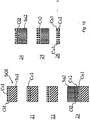
- the figures 12 to 17 illustrate methods of making a resonator 1 according to figure 1 .
- the process of figure 12 uses two silicon wafers of the silicon on SOI type.
- Each silicon-on-insulator SOI type wafer comprises a substrate Su1, Su2 surmounted by an insulating layer Ci1, Ci2 then by a layer of monocrystalline silicon Cs1, Cs2.
- the substrate Su1, Su2, can be made of silicon.
- a separation layer Co1 for example an amorphous SiO2 layer, is deposited on the silicon layer Cs1 of the first wafer.
- one or more mechanical resonator patterns are etched on the separation layer Co1 and on the silicon layer Cs1.
- a third step 23 the silicon layer Cs2 of the second wafer is sealed on the separation layer Co1.
- the second wafer is offset by an angle ⁇ relative to the first wafer before this sealing step 23 so that the directions Ds1, Ds2 of the crystal lattices are also offset by an angle ⁇ .
- the assembly is turned over and the substrate Su1 as well as the insulating layer Ci1 of the first wafer are removed.
- the layer of silicon Cs2 of the second wafer is etched with the pattern of mechanical resonators using the first layer of silicon Cs1 as an etching mask. The etching can be performed by a deep reactive ion etching technique (also known by the acronym DRIE for "Deep Reactive Ion Etching").
- DRIE deep reactive ion etching technique
- the figure 13 illustrates a production method also using two SOI wafers.
- steps 32 and 33 two parts Cop1, Cop2 of the separation layer Co1 are respectively deposited on each silicon layer Cs1, Cs2 of the two SOI wafers.
- steps 34, 35 the patterns of the resonator (s) are then etched on the two parts Cop1 and Cop2 of the separation layer Co1 as well as on the two layers of silicon Cs1, Cs2 of the two wafers.
- the two parts Cop1, Cop2 are then sealed with an offset ⁇ between the wafers so as to form the complete separation layer Co1.
- Steps 37, 38 consist of removing the two substrates Su1, Su2 as well as the two insulating layers Ci1, Ci2 in order to free the mechanical resonator (s).
- the figure 14 illustrates a production method using a single wafer of the double-SOI type.
- a double-SOI type wafer consists of a substrate Su1 surmounted by a first layer of insulator Ci1, a first layer of monocrystalline silicon Cs1, a second layer of insulator Ci2 then a second layer of monocrystalline silicon Cs2.
- the second insulating layer Ci2 thus performs the function of the separation and thermal compensation layer Co1 of the resonator 1.
- the first layer of silicon Cs1 and the second layer of silicon Cs2 comprise crystal lattices whose directions are offset by an angle ⁇ .
- a first step 41 consists in etching the mechanical resonator pattern in the second layer of silicon Cs2, the second layer of insulator Cs2 and the first layer of silicon Cs1.
- a second step 42 consists in removing the substrate Su1 and the first insulating layer Ci1 to free the mechanical resonator.
- the figure 15 illustrates a variant of the figure 14 using a double-SOI type wafer.
- a first step 51 consists in etching the pattern of mechanical resonators in the second layer of silicon Cs2 and the second layer of insulator Cs2.
- a wafer of silicon Si2 is sealed on the second layer of silicon Cs2.
- This Si2 silicon wafer is a sacrificial layer which only serves as a support for the structure and will be removed in a later step.
- the assembly is turned over and the substrate Su1 as well as the first insulating layer Ci1 of the first wafer are removed.
- the mechanical resonator pattern is etched on the first silicon layer Cs1 in a step 54 and, in a step 55, the silicon wafer Si2 is removed to release the mechanical resonator (s) 1.
- This variant of the method of the figure 14 can be implemented when the resonators 1 are too thick and the etching step 41 does not allow the first silicon layer Cs1 to be correctly etched.
- the figure 16 illustrates a production process using an SOI type wafer and an Si2 silicon wafer.
- a separation layer Co1 is deposited on the silicon layer Cs1 of the first wafer of SOI type.
- a pattern of mechanical resonators is etched on the separation layer Co1 and on the silicon layer Cs1.
- the silicon wafer Si2 is then sealed with an offset ⁇ on the separation layer Co1 in a step 63.
- Step 64 consists in thinning the silicon wafer Si2 until the height hs2 desired for the second silicon layer Cs2 is reached. of resonator 1.
- a step 65 the pattern of mechanical resonator 1 is etched on the second silicon layer Cs2 formed by the silicon wafer Si2 and, in a step 66, the substrate Su1 and the insulating layer Ci1 are removed to release the mechanical resonator (s).
- the figure 17 illustrates a production method using a single wafer of the SOI type in which the substrate Su1 is made of silicon and forms the second layer of silicon Cs2.
- the separation layer Co1 is formed by an insulating layer Ci1 preferably made of silicon oxide.
- a first step 71 consists in thinning the substrate Su1 until the desired height hs2 is reached for the second layer of silicon Cs2.
- the pattern of one or more mechanical resonators is etched on the silicon layer Cs1.
- a structuring layer Cst is then deposited on the thinned substrate Su1 in a step 73 in order to stiffen the structure, then the pattern of mechanical resonators is etched in the layers of insulation Ci1 and of substrate Su1 in a step 74.
- the structuring layer Cst is removed to free the mechanical resonators 1.
- an external thermal compensation layer can be produced in a silicon oxidation chamber thus forming a layer of silicon oxide around resonator 1.
- the production of a second separation layer Co2 and a third layer of silicon Cs3 can be achieved, for example, by the sealing of a third silicon-on-insulator type wafer and by corresponding additional etching steps.
Description
L'invention concerne un résonateur mécanique destiné à équiper un organe régulateur d'une pièce d'horlogerie ainsi qu'un procédé de fabrication d'un tel résonateur.The invention relates to a mechanical resonator intended to equip a regulating member of a timepiece and to a method of manufacturing such a resonator.
L'invention trouve une application particulièrement avantageuse pour les résonateurs avec symétrie radiale oscillant en « breathing mode ». Plus spécifiquement l'invention trouve une application particulièrement avantageuse pour les spiraux destinés à équiper le balancier d'un ensemble d'horlogerie mécanique telle qu'une montre.The invention finds a particularly advantageous application for resonators with radial symmetry oscillating in “breathing mode”. More specifically, the invention finds a particularly advantageous application for balance springs intended to equip the balance of a mechanical timepiece assembly such as a watch.
Les mouvements de montres mécaniques sont régulés au moyen d'un régulateur mécanique comprenant un résonateur, c'est-à-dire un composant déformable élastiquement et dont les oscillations déterminent la marche de la montre. De nombreuses montres comportent par exemple un régulateur comprenant un spiral comme résonateur, monté sur l'axe d'un balancier et mis en oscillation grâce à un échappement; la fréquence propre du couple balancier-spiral permet de réguler la montre. D'autres types de résonateurs connus sont basés par exemple sur des diapasons, des barreaux oscillants, ou d'autres éléments mécaniques.The movements of mechanical watches are regulated by means of a mechanical regulator comprising a resonator, that is to say an elastically deformable component whose oscillations determine the rate of the watch. Many watches include, for example, a regulator comprising a hairspring as resonator, mounted on the axis of a balance and set in oscillation by means of an escapement; the natural frequency of the balance-spring pair makes it possible to regulate the watch. Other known types of resonators are based, for example, on tuning forks, oscillating bars, or other mechanical elements.
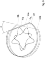
Un exemple de résonateur spiral 1 est illustré sur la ![]()
- ϕ, l'angle de torsion du ressort et
- M, le couple de rappel du ressort spiral.
- ϕ, the torsion angle of the spring and
- M, the return torque of the spiral spring.
L'équation de ce couple de rappel pour un barreau constitué d'un matériau spécifique est donné par : 
- E, le module d'Young du matériau employé pour le barreau,
- L, la longueur du barreau,
- w, la largeur du barreau, et
- t, l'épaisseur du barreau.
- E, the Young's modulus of the material used for the bar,
- L, the length of the bar,
- w , the width of the bar, and
- t , the thickness of the bar.
La fréquence propre de résonance du spiral est proportionnelle à la racine carrée de sa raideur. Par conséquent, la fréquence du spiral est proportionnelle à la racine carrée du module d'Young du matériau. Donc, si le module d'Young varie en fonction de la température, la fréquence du spiral va également varier en fonction de la température. Pour une faible variation en température, la fréquence du spiral dépend donc au premier ordre de la variation en température du module d'Young.The natural resonant frequency of the balance spring is proportional to the square root of its stiffness. Consequently, the frequency of the hairspring is proportional to the square root of the Young's modulus of the material. So, if the Young's modulus varies as a function of temperature, the frequency of the hairspring will also vary as a function of temperature. For a weak variation in temperature, the frequency of the hairspring therefore depends in the first order on the variation in temperature of the Young's modulus.
Il est ainsi admis que l'équation suivante montre les variations du module d'Young en fonction de la température : ![]()
- ∝ E , le coefficient thermique du module d'Young,
- E, le module d'Young à la température T, et
- E 0 , le module d'Young à la température T 0.
- ∝ E , the thermal coefficient of the Young modulus,
- E, Young's modulus at temperature T , and
- E 0 , the Young modulus at temperature T 0 .
Afin de conserver une fréquence d'oscillation stable même en cas de variations de température, et donc de maintenir l'isochronisme, il est connu de réaliser des spiraux ou d'autres types de résonateurs mécaniques dans un métal tel que l'élinvar qui est caractérisé par un module d'Young extrêmement stable en fonction de la température.In order to maintain a stable oscillation frequency even in the event of temperature variations, and therefore to maintain isochronism, it is known practice to produce balance springs or other types of mechanical resonators in a metal such as elinvar which is characterized by an extremely stable Young's modulus as a function of temperature.
Il est également connu de réaliser des résonateurs par gravure d'un wafer de silicium qui peuvent être usinés avec une très haute précision par des procédés de photolithographie. Les procédés de réalisation de ces résonateurs mécaniques utilisent généralement des wafers de silicium monocristallin. Le silicium monocristallin appartient en effet à la classe cristalline cubique m3m dont le coefficient d'expansion thermique (alpha) est totalement isotrope.It is also known to produce resonators by etching a silicon wafer which can be machined with very high precision by photolithography processes. The methods of making these mechanical resonators generally use monocrystalline silicon wafers. Monocrystalline silicon indeed belongs to the cubic crystal class m3m, the coefficient of thermal expansion (alpha) of which is totally isotropic.
Le silicium présente une valeur du premier coefficient thermoélastique très négative, proche de -64 ppm/C. Par conséquent, la raideur d'un résonateur en silicium, et donc sa fréquence propre, varie fortement selon la température. Un résonateur mécanique en silicium pur est donc anisochrone.Silicon has a very negative first thermoelastic coefficient value, close to -64 ppm / C. Consequently, the stiffness of a silicon resonator, and therefore its natural frequency, varies greatly with temperature. A pure silicon mechanical resonator is therefore anisochronous.
Afin de compenser au moins partiellement cet inconvénient,
Ce document
La coupe {001} présente un facteur d'anisotropie planaire relativement élevé. La situation est illustrée sur la
Cela se traduit par une rigidité à la flexion (module d'Young) qui varie significativement en fonction de la direction. En raison de cette anisotropie, un résonateur spiral oscillant en breathing mode et gravé dans un wafer coupé selon le plan {001} a un développement non concentrique, ce qui perturbe la chronométrie et l'esthétique.This results in a bending stiffness (Young's modulus) which varies significantly as a function of the direction. Due to this anisotropy, a spiral resonator oscillating in breathing mode and engraved in a wafer cut according to the {001} plane has a non-concentric development, which disturbs the chronometry and the aesthetics.
L'anisotropie du module d'Young planaire d'un résonateur gravé dans un wafer coupé selon le plan {001} est également gênante si l'on veut maitriser correctement la raideur équivalente d'un résonateur de forme complexe lors de sa phase de conception. En effet, pour obtenir une bonne corrélation entre les valeurs calculées et les valeurs mesurées pour la raideur équivalente, on doit tenir compte notamment de l'orientation précise des éléments du résonateur qui ne présentent pas une symétrie parfaitement radiale par rapport aux différentes directions planaires du wafer. Par exemple les courbes terminales de deux spiraux orientés différemment dans un wafer coupé selon le plan {001} verront un module d'Young en flexion significativement diffèrent et en conséquence leur raideurs équivalentes seront aussi significativement différentes, comme illustré schématiquement sur la
Il est aussi à noter que les modes de vibration autres que fondamentaux sont des sources de dissipation d'énergie. Les mouvements non concentriques d'un spiral provoquent le déplacement des pivots de balancier dans les pierres et augmentent par voie de conséquence les forces de frottement.It should also be noted that the modes of vibration other than fundamental are sources of energy dissipation. The non-concentric movements of a hairspring cause the movement of the balance pivots in the stones and consequently increase the frictional forces.
Par ailleurs, des inconvénients similaires seraient obtenus en découpant un résonateur dans un wafer orienté selon la direction cristalline <110> d'un cristal de silicium. Dans ce cas, la valeur moyenne du module d'Young serait de 165 GPa. La coupe {110}, et les coupes équivalentes {101} et {011}, sont illustrées sur la
Afin de palier au moins partiellement à ces problèmes,
L'anisotropie du cristal de silicium influence dans une moindre mesure la sensibilité à la température du module d'Young. Le premier coefficient thermique, soit la dérivée dE/dT du module d'Young par rapport à la température, est certes isotrope quel que soit le plan cristallin de la coupe {110}, {111} ou {001} (
La croissance d'une couche d'oxyde sur le spiral de
Le silicium est un matériau fragile avec des contraintes de rupture en flexion inférieures à 10 GPa et en fatigue de l'ordre de 2 à 3 GPa. La présence d'angles vifs dans les structures typiques d'un résonateur en silicium est à l'origine de fortes concentrations de contraintes, qui peuvent rapidement produire des déformations et accélérer la rupture.
Dans toutes les solutions décrites ci-dessus, la présence d'une couche d'oxyde relativement épaisse (environ 8% de l'épaisseur totale du spiral) résulte en un spiral avec un état de surface foncé et mat, souvent considéré inesthétique.In all of the solutions described above, the presence of a relatively thick oxide layer (about 8% of the total thickness of the hairspring) results in a hairspring with a dark and matt surface finish, often considered unsightly.
De plus la croissance d'une couche d'oxyde à la surface d'un spiral en silicium se déroule à haute température, typiquement à 1100°C. Les dimensions originales du composant en silicium se dilatent sous l'effet de la chaleur et proportionnellement au coefficient de dilation thermique αSi. La croissance de l'oxyde se déroule donc sur un composant aux dimensions dilatées. Le retour à température ambiante en fin de procédé se déroule sur un composant composite, formé d'un noyau silicium et de la couche d'oxyde périphérique nouvellement formée. Le coefficient de dilation thermique de l'oxyde de silicium étant αSiO2 différent de celui du silicium αSi(αSi> αSiO2), il s'ensuit une élongation résiduelle des dimensions et une mise sous contrainte du composant. Ceci est particulièrement vrai dans le cas du spiral en silicium où l'élongation de la longueur du spiral peut atteindre des valeurs de l'ordre de 0.2%, modifiant ainsi l'angle de pitonnage, et provoquant la déformation de la géométrie du spiral sous les effets de la contrainte.In addition, the growth of an oxide layer on the surface of a silicon hairspring takes place at high temperature, typically at 1100 ° C. The original dimensions of the silicon component expand under the effect of heat and in proportion to the coefficient of thermal expansion α Si . The growth of the oxide therefore takes place on a component with dimensions dilated. The return to ambient temperature at the end of the process takes place on a composite component, formed of a silicon core and the newly formed peripheral oxide layer. The coefficient of thermal expansion of silicon oxide being α SiO2 different from that of silicon α Si (α Si > α SiO2 ), there follows a residual elongation of the dimensions and a stressing of the component. This is particularly true in the case of the silicon hairspring where the elongation of the length of the hairspring can reach values of the order of 0.2%, thus modifying the pitonning angle, and causing the deformation of the geometry of the hairspring under the effects of coercion.
Un but de la présente invention est de proposer un résonateur mécanique, notamment pour l'organe régulateur d'un mouvement d'horlogerie mécanique, qui permette d'éviter les inconvénients ci-dessus, ou en tout cas d'offrir un meilleur compromis entre ces inconvénients.An object of the present invention is to provide a mechanical resonator, in particular for the regulating member of a mechanical clockwork movement, which makes it possible to avoid the above drawbacks, or in any case to offer a better compromise between these disadvantages.
En particulier, un but de la présente invention est de proposer un nouveau résonateur mécanique.In particular, an aim of the present invention is to provide a new mechanical resonator.
En particulier, un but de la présente invention est de proposer un résonateur mécanique thermocompensé.In particular, an aim of the present invention is to provide a thermocompensated mechanical resonator.
Un autre but est de proposer un résonateur mécanique moins fragile que les résonateurs réalisés en silicium ou en silicium oxydé en surface.Another aim is to provide a mechanical resonator that is less fragile than resonators made of silicon or of silicon oxidized at the surface.
Un autre but est de proposer un résonateur mécanique dont le développement est concentrique.Another aim is to provide a mechanical resonator whose development is concentric.
Un autre but est de proposer un résonateur mécanique dont la concentricité du développement est peu affectée par la température.Another aim is to provide a mechanical resonator whose development concentricity is little affected by temperature.
Un autre but est de proposer un résonateur mécanique plus rapide à produire.Another aim is to provide a mechanical resonator that is faster to produce.
Un but est aussi de pallier les inconvénients cités auparavant et donc de proposer un oscillateur mécanique en silicium monocristallin, simple à fabriquer, dont les caractéristiques mécaniques sont similaires dans toutes les directions d'un plan.An aim is also to overcome the drawbacks mentioned above and therefore to propose a mechanical oscillator in monocrystalline silicon, simple to manufacture, the mechanical characteristics of which are similar in all directions of a plane.
Un autre but est de proposer un résonateur mécanique aux dimensions plus précises et présentant moins de contraintes résiduelles.Another aim is to provide a mechanical resonator with more precise dimensions and exhibiting fewer residual stresses.
Selon un aspect, ces buts sont atteints au moyen d'un résonateur mécanique, notamment pour l'organe régulateur d'un mouvement d'horlogerie mécanique, le résonateur comprenant:
- (i) une première couche de silicium découpé selon un premier plan cristallin du silicium ;
- (ii) une deuxième couche de silicium découpée selon un deuxième plan cristallin du silicium ; (iii) au moins une couche de séparation entre les première et deuxième couches de silicium ;
le premier plan cristallin étant différent et non équivalent au deuxième plan cristallin.According to one aspect, these aims are achieved by means of a mechanical resonator, in particular for the regulating member of a mechanical clockwork movement, the resonator comprising:
- (i) a first layer of silicon cut along a first crystalline plane of silicon;
- (ii) a second layer of silicon cut along a second crystalline plane of silicon; (iii) at least one separation layer between the first and second layers of silicon;
the first crystal plane being different and not equivalent to the second crystal plane.
Une couche de silicium est dite découpée selon un plan cristallin donné du silicium si elle a été obtenue par gravage d'un wafer découpé selon ce plan.A silicon layer is said to be cut along a given crystalline plane of silicon if it has been obtained by etching a wafer cut along this plane.
Des réseaux cristallins sont décalés d'un angle α lorsque les directions cristallines correspondantes ou équivalentes sont décalées d'un angle α.Crystal lattices are shifted by an angle α when the corresponding or equivalent crystal directions are shifted by an angle α.
Les « directions cristallines » (ou directions nodales) des couches correspondent aux directions des vecteurs [xyz] joignant les nœuds n du cristal. Le silicium ayant une structure cristalline à symétrie cubique, les quatre diagonales sont équivalentes, les trois faces du cube sont équivalentes, etc. Par exemple, les directions [100], [1-00], [010], [01-0], [001], [001] et [001-] sont équivalentes entre elles et désignées par une famille de directions <100> (l'opérateur - désignant l'opposition).The “crystal directions” (or nodal directions) of the layers correspond to the directions of the vectors [xyz] joining the nodes n of the crystal. Since silicon has a crystal structure with cubic symmetry, the four diagonals are equivalent, the three faces of the cube are equivalent, etc. For example, the directions [100], [1 - 00], [010], [01 - 0], [001], [001] and [001 - ] are equivalent to each other and designated by a family of directions <100 > (the operator - designating the opposition).
Des plans sont dits équivalents s'ils peuvent être obtenus par permutations et/ou oppositions des indices. Le plan (xyz) est perpendiculaire à la direction [xyz]. Par exemple, les plans (100), (1-00), (010), (01-0), (001), (001) et (001-), sont équivalents et forme une famille de plans désignée par {100} (l'opérateur - désignant l'opposition).Plans are said to be equivalent if they can be obtained by permutations and / or oppositions of the indices. The plane (xyz) is perpendicular to the direction [xyz]. For example, the planes (100), (1 - 00), (010), (01 - 0), (001), (001) and (001 - ), are equivalent and form a family of planes designated by {100 } (the operator - designating the opposition).
La robustesse mécanique est renforcée du fait que le résonateur n'est pas constitué d'une structure monocristalline et monolithique mais de plusieurs couches monocristallines de réseaux cristallins séparées entre elles par une ou plusieurs couches de séparation. Ainsi, une fissure générée dans une couche de silicium cristallin peut être arrêtée par la couche de séparation, et éviter de se propager à l'autre couche cristalline.The mechanical robustness is enhanced by the fact that the resonator does not consist of a monocrystalline and monolithic structure but of several monocrystalline layers of crystal lattices separated from one another by one or more separation layers. Thus, a crack generated in one crystalline silicon layer can be stopped by the separating layer, and avoid propagating to the other crystalline layer.
Selon la première alternative revendiquée dans laquelle les réseaux cristallins des deux couches sont décalés angulairement, la robustesse mécanique est renforcée. Ainsi, une fissure générée dans une couche de silicium cristallin et qui aurait traversé la ou les couches de séparation a moins de risque de se propager dans l'autre couche de silicium cristallin, en raison des déphasages entre les plans de fissuration.According to the first claimed alternative in which the crystal lattices of the two layers are angularly offset, the mechanical robustness is enhanced. Thus, a crack generated in a layer of crystalline silicon and which would have passed through the separation layer or layers has less risk of propagating into the other layer of crystalline silicon, due to the phase shifts between the cracking planes.
Selon la deuxième alternative, la robustesse mécanique est aussi renforcée grâce au gravage des différentes couches de silicium du résonateur dans des plans cristallins différents et non équivalents.According to the second alternative, the mechanical robustness is also reinforced thanks to the etching of the different layers of silicon of the resonator in different and non-equivalent crystalline planes.
Par exemple, selon cette deuxième alternative, la première couche de silicium peut être gravée dans un wafer découpé selon le plan {001} et la deuxième couche de silicium dans un wafer découpé selon le plan {011} ou selon le plan {111}. Alternativement, la première couche de silicium peut être gravée dans un wafer découpé selon le plan {011} et la deuxième couche de silicium dans un wafer gravé selon le plan {111}. Selon ces modes de réalisation, les orientations cristallines sont par essence différentes et il existe intrinsèquement un décalage angulaire des réseaux respectifs qui favorise la robustesse de la structure.For example, according to this second alternative, the first silicon layer can be etched in a wafer cut along the {001} plane and the second silicon layer in a wafer cut along the {011} plane or along the {111} plane. Alternatively, the first silicon layer can be etched in a wafer cut along the {011} plane and the second silicon layer in a wafer etched along the {111} plane. According to these embodiments, the crystal orientations are essentially different and there is intrinsically an angular offset of the respective networks which favors the robustness of the structure.
Au moins une couche de séparation peut être constituée d'un matériau amorphe. Un matériau amorphe réduit encore le risque de propagation de fissures.At least one release layer can be made of an amorphous material. Amorphous material further reduces the risk of crack propagation.
En choisissant, par exemple, une couche de séparation isotrope dans le plan, celle-ci présente un module d'Young également isotrope. Cette couche de séparation compense donc de manière homogène les variations de raideur subies par le résonateur, et n'ajoute pas d'anisotropie indésirable.By choosing, for example, an isotropic separation layer in the plane, the latter has a Young's modulus which is also isotropic. This separation layer therefore homogeneously compensates for the variations in stiffness undergone by the resonator, and does not add undesirable anisotropy.
Au moins une couche de séparation présente de préférence un premier coefficient thermique du module d'Young isotrope dans le plan de la couche.At least one separation layer preferably has a first thermal coefficient of the isotropic Young's modulus in the plane of the layer.
Au moins une couche de séparation présente de préférence un deuxième coefficient thermique du module d'Young isotrope dans le plan de la couche.At least one separation layer preferably has a second thermal coefficient of the Young's modulus isotropic in the plane of the layer.
Dans un autre mode de réalisation, au moins une couche de séparation présente un module d'Young, ou un deuxième coefficient thermique du module d'Young, anisotrope dans son plan. La couche de séparation est alors de préférence orientée par rapport aux couches de silicium de manière à ce qu'elle compense l'anisotropie résiduelle du module d'Young, et/ou l'anisotropie résiduelle du deuxième coefficient thermique du module d'Young.In another embodiment, at least one separating layer has a Young's modulus, or a second thermal coefficient of the Young's modulus, anisotropic in its plane. The separation layer is then preferably oriented relative to the silicon layers so that it compensates for the residual anisotropy of the Young's modulus, and / or the residual anisotropy of the second thermal coefficient of the Young's modulus.
Au moins une couche de séparation peut être constituée d'un matériau présentant un coefficient thermique du module d'Young de signe opposé à celui du silicium. Ainsi la thermocompensation du résonateur mécanique ne se fait pas, ou pas uniquement, par l'intermédiaire d'une couche de SiO2 extérieure mais également par l'intermédiaire d'au moins une couche de séparation enterrée.At least one separating layer can be made of a material having a thermal coefficient of Young's modulus of sign opposite to that of silicon. Thus the thermocompensation of the mechanical resonator does not take place, or not only, by means of an outer SiO2 layer but also by means of at least one buried separation layer.
Au moins une couche de séparation peut être constituée de SiO2. La présence d'une couche d'oxyde enterrée ab initio, avant la réalisation du composant et la formation de l'oxyde périphérique, limite de facto l'élongation du noyau en silicium en phase de montée en température d'oxydation, et par voie de conséquence la dilation résiduelle et le développement de contrainte au retour à la température ambiante. Cette solution est particulièrement avantageuse dans le cas de composants dont la dilatation thermique serait catastrophique, par exemple dans le cas du flambage de poutres encastrées aux deux extrémités. L'oxydation de dispositifs faisant appel à ce type d'éléments, comme les guidages flexibles, est très limitée.At least one separation layer can consist of SiO2. The presence of an oxide layer buried ab initio, before the component is made and the peripheral oxide is formed, de facto limits the elongation of the silicon core during the oxidation temperature rise phase, and by as a consequence the residual expansion and the development of stress on return to ambient temperature. This solution is particularly advantageous in the case of components whose thermal expansion would be catastrophic, for example in the case of the buckling of beams embedded at both ends. The oxidation of devices using this type of element, such as flexible guides, is very limited.
Le résonateur peut comprendre plus de deux couches de silicium séparées les unes des autres.The resonator can include more than two layers of silicon separated from each other.
Le résonateur peut comprendre plusieurs couches de séparation entre deux couches de silicium.The resonator can comprise several separation layers between two layers of silicon.
Le résonateur peut comporter une couche externe constituée d'un matériau présentant un coefficient thermique du module d'Young de signe opposé à celui du silicium. L'utilisation de la couche de séparation effectuant une compensation thermique entre les première et deuxième couches de silicium permet de limiter l'épaisseur de cette couche externe. L'épaisseur de cette couche externe est supérieure à l'épaisseur de l'oxyde de silicium natif résultant de l'oxydation naturelle du silicium à température ambiante.The resonator may include an outer layer made of a material having a thermal coefficient of the Young's modulus of sign opposite to that of silicon. The use of the separating layer performing thermal compensation between the first and second silicon layers makes it possible to limit the thickness of this outer layer. The thickness of this outer layer is greater than the thickness of the native silicon oxide resulting from the natural oxidation of silicon at room temperature.
Le résonateur peut être un résonateur mécanique à symétrie radiale.The resonator can be a radially symmetrical mechanical resonator.
Le résonateur peut être un résonateur mécanique de type spiral.The resonator can be a mechanical resonator of the spiral type.
Selon les modes de réalisation de l'invention, au moins certains des avantages suivants peuvent être obtenus :According to the embodiments of the invention, at least some of the following advantages can be obtained:
- A) Maitrise des oscillations et oscillations concentriques dans le cas de résonateurs à symétrie radiale.A) Control of oscillations and concentric oscillations in the case of radial symmetry resonators.
- B) Meilleure corrélation entre résultats de simulation lors du design du résonateur et résultats expérimentaux.B) Better correlation between simulation results during the design of the resonator and experimental results.
- C) Libre orientation de secteurs asymétriques du résonateur par rapport au plan du wafer.C) Free orientation of asymmetric sectors of the resonator with respect to the plane of the wafer.
- D) Meilleur rendu esthétique des résonateurs en battement.D) Better aesthetic rendering of the resonators in beat.
- A) Moins d'oxyde nécessaire pour la thermocompensation en surface des résonateurs.A) Less oxide required for thermocompensation on the surface of the resonators.
- B) Temps de cycle de fabrication plus courts.B) Shorter manufacturing cycle times.
- C) Meilleure qualité de l'oxyde en surface (composition, structure et état de surface).C) Better quality of the oxide on the surface (composition, structure and surface condition).
- D). Meilleur contrôle des contraintes résiduelles et limitation des défauts dimensionnels (élongation du ressort) lors de la mise en forme comportant la gravure DRIE et l'oxydation du composant à haute températureD). Better control of residual stresses and limitation of dimensional defects (spring elongation) during shaping including DRIE etching and oxidation of the component at high temperature
- A) Meilleure robustesse mécanique du système.A) Better mechanical robustness of the system.
- B) Retarder la propagation de fissures et la casse prématurée du ressort.B) Delay the propagation of cracks and the premature breakage of the spring.
L'invention a aussi pour objet un procédé de fabrication d'un résonateur mécanique.The subject of the invention is also a method of manufacturing a mechanical resonator.
Selon un mode de réalisation, le procédé de fabrication d'un résonateur mécanique comporte la déposition d'une couche de séparation sur un wafer de silicium, puis la gravure de plusieurs résonateurs mécanique dans ce wafer. La couche de séparation peut être par exemple une couche de compensation thermique, par exemple une couche de SiO2. La couche de compensation thermique est ainsi déposée en une seule opération sur tous les résonateurs produits à partir d'un wafer, ce qui réduit le temps de fabrication et le risque de briser les résonateurs lors de leurs manipulations après leur gravure.According to one embodiment, the method of manufacturing a mechanical resonator comprises the deposition of a separation layer on a silicon wafer, then the etching of several mechanical resonators in this wafer. The separation layer may for example be a thermal compensation layer, for example a layer of SiO2. The thermal compensation layer is thus deposited in a single operation on all the resonators produced from a wafer, which reduces the manufacturing time and the risk of breaking the resonators during their handling after their etching.
Au sens de l'invention, on entend par « déposer une couche de matériau », les procédés consistants à ajouter de la matière par dépôt, ajouter de la matière par croissance et transformation de la matière existante ou le report d'une couche annexe par scellement de la couche annexe.For the purposes of the invention, the term “depositing a layer of material” is understood to mean the processes consisting in adding material by deposition, adding material by growth and transformation of the existing material or the transfer of an additional layer by sealing of the annex layer.
Le procédé peut comporter la déposition d'une deuxième couche de silicium sur la couche de séparation, les résonateurs mécaniques étant gravés après cette déposition.The method may include the deposition of a second layer of silicon on the separation layer, the mechanical resonators being etched after this deposition.
Le procédé peut comporter la déposition d'une deuxième couche de silicium sur la couche de séparation après ladite étape de gravure des résonateurs mécaniques. La première couche de silicium peut alors être utilisée comme masque pour la gravure de la deuxième couche de silicium.The method may include the deposition of a second layer of silicon on the separation layer after said step of etching the mechanical resonators. The first layer of silicon can then be used as a mask for etching the second layer of silicon.
Le procédé peut comporter le scellement de plusieurs wafers de silicium dont l'un au moins est recouvert d'une couche de séparation, par exemple d'une couche de SiO2, puis la gravure d'une pluralité de résonateurs dans cet empilement.The method may include the sealing of several silicon wafers, at least one of which is covered with a separation layer, for example a layer of SiO2, then the etching of a plurality of resonators in this stack.
Des exemples de mise en œuvre de l'invention sont indiqués dans la description illustrée par les figures annexées dans lesquelles :
- La
figure 1 illustre à titre d'exemple un résonateur mécanique, ici un spiral. - La
figure 2 indique la valeur E du module d'Young selon les différentes directions d'un plan {001}, ainsi que sa valeur moyenne E(moyen). - La
figure 3 indique la valeur E du module d'Young selon les différentes direction du plan {111}, ainsi que sa valeur moyenne E(moyen). - La
figure 4 illustre la variation de raideur de la courbe terminale d'un spiral selon différentes orientations du spiral dans le plan {001}. - La
figure 5 illustre la variation dE/dT du premier coefficient thermique du module d'Young pour un wafer coupé dans les plans {001}, {011} ou {111}. Ce premier coefficient est anisotrope et sa valeur moyenne dE/dT(moyen) ne diffère donc pas de la valeur absolue pour chaque direction. - La
figure 6 illustre la variation d2E/dT2 du deuxième coefficient thermique du module d'Young pour un wafer coupé dans les plans {001}, {011} ou {111}, ainsi que sa valeur moyenne. - La
figure 7 illustre une section transversale d'une portion d'un résonateur, par exemple la section d'une spire d'un spiral, gravé ici dans deux couches de silicium monocristallin coupées dans des plans similaires mais dont les réseaux cristallins sont décalés de 30° - La
figure 8 illustre une section transversale d'une portion d'un résonateur, par exemple la section d'une spire d'un spiral, gravé ici dans trois couches de silicium découpées selon des plans différents ({001} ou {111}) et séparées les unes des autres par des couches de SiO2 enterrées. Dans cet exemple, il n'y a pas de décalage angulaire de la direction entre les deux couches découpées selon le plan {001}. - La
figure 9 illustre schématiquement deux wafers de silicium découpés dans le plan {001} dont les réseaux cristallins sont décalés de 30°, ainsi que le module d'Young planaire EA, EB des deux wafers. - La
figure 10 illustre schématiquement, en 2D, trois wafers de silicium coupés dans le plan {001} dont les réseaux cristallins sont décalés de 30°, ainsi que le module d'Young planaire EA, EB, Ec des trois wafers. - La
figure 11 illustre schématiquement les directions cristallines dans un cristal cubique. Les directions cristallines sont définies de la même façon dans un cristal cubique à face centrée, tel que le silicium. - La
figure 12 est une représentation schématique du procédé de réalisation d'un résonateur mécanique selon un premier mode de réalisation ; - La
figure 13 est une représentation schématique du procédé de réalisation d'un résonateur mécanique selon un deuxième mode de réalisation ; - La
figure 14 est une représentation schématique du procédé de réalisation d'un résonateur mécanique selon un troisième mode de réalisation ; - La
figure 15 est une représentation schématique du procédé de réalisation d'un résonateur mécanique selon un quatrième mode de réalisation ; - La
figure 16 est une représentation schématique du procédé de réalisation d'un résonateur mécanique selon un cinquième mode de réalisation ; et - La
figure 17 est une représentation schématique du procédé de réalisation d'un résonateur mécanique selon un sixième mode de réalisation.
- The
figure 1 illustrates by way of example a mechanical resonator, here a balance spring. - The
figure 2 indicates the value E of the Young modulus according to the different directions of a {001} plane, as well as its mean value E (average). - The
figure 3 indicates the value E of the Young modulus according to the different directions of the {111} plane, as well as its mean value E (average). - The
figure 4 illustrates the variation in stiffness of the end curve of a hairspring according to different orientations of the hairspring in the {001} plane. - The
figure 5 illustrates the variation dE / dT of the first thermal coefficient of the Young's modulus for a wafer cut in the {001}, {011} or {111} planes. This first coefficient is anisotropic and its mean value dE / dT (mean) therefore does not differ from the absolute value for each direction. - The
figure 6 illustrates the variation d 2 E / dT 2 of the second thermal coefficient of the Young's modulus for a wafer cut in the {001}, {011} or {111} planes, as well as its mean value. - The
figure 7 illustrates a cross section of a portion of a resonator, for example the section of a turn of a balance spring, etched here in two layers of monocrystalline silicon cut in similar planes but whose crystal lattices are offset by 30 ° - The
figure 8 illustrates a cross section of a portion of a resonator, for example the section of a turn of a balance spring, etched here in three layers of silicon cut according to different planes ({001} or {111}) and separated from each other by buried SiO2 layers. In this example, there is no angular offset in the direction between the two layers cut along the {001} plane. - The
figure 9 schematically illustrates two silicon wafers cut in the {001} plane whose crystal lattices are offset by 30 °, as well as the planar Young's modulus E A , E B of the two wafers. - The
figure 10 schematically illustrates, in 2D, three silicon wafers cut in the {001} plane whose crystal lattices are offset by 30 °, as well as the planar Young's modulus E A , E B , Ec of the three wafers. - The
figure 11 schematically illustrates the crystal directions in a cubic crystal. Crystal directions are similarly defined in a face-centered cubic crystal, such as silicon. - The
figure 12 is a schematic representation of the method of making a mechanical resonator according to a first embodiment; - The
figure 13 is a schematic representation of the method for producing a mechanical resonator according to a second embodiment; - The
figure 14 is a schematic representation of the method of making a mechanical resonator according to a third embodiment; - The
figure 15 is a schematic representation of the method of making a mechanical resonator according to a fourth embodiment; - The
figure 16 is a schematic representation of the method of making a mechanical resonator according to a fifth embodiment; and - The
figure 17 is a schematic representation of the method for producing a mechanical resonator according to a sixth embodiment.
La
La première couche de silicium Cs1 s'étend sur une hauteur hs1 et sur toute la largeur L du résonateur 1. La deuxième couche de silicium Cs2 s'étend sur une hauteur hs2 sensiblement égale à la hauteur hs1 et sur toute la largeur L. La couche de séparation Co1 s'étend sur une hauteur ho1 très inférieure aux deux hauteurs hs1, hs2 et sur toute la largeur L.The first layer of silicon Cs1 extends over a height hs1 and over the entire width L of the
Il est aussi possible de prévoir plusieurs couches de séparation entre les deux couches de silicium Cs1, Cs2.It is also possible to provide several separation layers between the two layers of silicon Cs1, Cs2.
Dans cet exemple, la première couche de silicium Cs1 et la deuxième couche de silicium proviennent de wafers découpés selon le même plan cristallin, de préférence le plan {001}, ou le plan {011}. Il est aussi possible de prévoir un empilement de couches de silicium obtenues à partir de wafers découpés selon des plans cristallins différents; par exemple une couche découpée dans un wafer {001} et une autre couche découpée dans un wafer {011}.In this example, the first layer of silicon Cs1 and the second layer of silicon come from wafers cut along the same crystal plane, preferably the {001} plane, or the {011} plane. It is also possible to provide a stack of silicon layers obtained from wafers cut along different crystal planes; for example a layer cut from a wafer {001} and another layer cut from a wafer {011}.
Le réseau cristallin Ds1 de la première couche de silicium Cs1 est décalée d'un angle α par rapport au réseau cristallin Ds2 de la deuxième couche de silicium Cs2. Les directions Ds1, Ds2 sont définies à partir de n'importe quel vecteur cristallin correspondants dans les couches Cs1, Cs2.The crystal lattice Ds1 of the first layer of silicon Cs1 is offset by an angle α with respect to the crystal lattice Ds2 of the second layer of silicon Cs2. The directions Ds1, Ds2 are defined from any corresponding crystal vector in the layers Cs1, Cs2.
Les hachures des
La couche de séparation Co1 est avantageusement constituée d'un matériau présentant un coefficient thermique du module d'Young de signe opposé à celui du silicium de sorte que la variation de la raideur des couches de silicium Cs1, Cs2 en fonction de la température soit, au moins partiellement, compensée par la couche de séparation Co1. De préférence, la couche de séparation Co1 est formée d'oxyde de silicium. Le coefficient thermique du module d'Young pour le silicium est de
-64.10-6K-1 et le coefficient thermique du module d'Young pour l'oxyde de silicium est de 187,5.10-6K-1 à une température ambiante, environ 20°C. Ainsi, pour compenser, au moins partiellement, la variation de la raideur des couches de silicium Cs1, Cs2 en fonction de la température, le rapport volumique entre la couche de séparation et de compensation thermique Co1 et les couches de silicium Cs1, Cs2 est avantageusement d'au moins 5%, de préférence au moins 10%, par exemple plus de 20%, à une température ambiante de 20°C. Sur la
-64.10 -6 K -1 and the thermal coefficient of Young's modulus for silicon oxide is 187.5.10 -6 K -1 at room temperature, approximately 20 ° C. Thus, to compensate, at least partially, the variation in the stiffness of the silicon layers Cs1, Cs2 as a function of the temperature, the volume ratio between the separation and thermal compensation layer Co1 and the silicon layers Cs1, Cs2 is advantageously at least 5%, preferably at least 10%, for example more than 20%, at an ambient temperature of 20 ° C. On the
La
La plupart des wafers de silicium présentent un méplat, représenté par les références 20A respectivement 20B sur la
La
Dans cet exemple, la première couche de silicium Cs1 et la troisième couche de silicium sont gravées dans des wafers découpés selon le même plan cristallin, de préférence le plan {001}, ou de la famille {011}. La deuxième couche de silicium est quant à elle gravée dans un wafer selon le plan cristallin {111} qui possède des propriétés thermoélastiques plus homogènes dans toutes les directions du plan. La compensation des variations du module d'Young selon la direction se fait donc avant tout entre les couches Cs1 et Cs3.In this example, the first layer of silicon Cs1 and the third layer of silicon are etched in wafers cut along the same crystal plane, preferably the {001} plane, or of the {011} family. The second silicon layer is for its part etched in a wafer along the {111} crystal plane which has more homogeneous thermoelastic properties in all directions of the plane. The compensation of the variations of the Young's modulus according to the direction is thus done above all between the layers Cs1 and Cs3.
Les couches Cs1 à Cs3 peuvent cependant correspondre à n'importe quel plan de coupe ou combinaison de plans de coupe des familles de plan {110}, {111} et {001}. Dans un autre mode de réalisation, les couches correspondent à une combinaison des plans de coupe des familles {110} et {001}. Dans un mode de réalisation préférentiel l'ensemble des couches correspondent au plan des familles {001}, décalées angulairement les unes des autres de manière à homogénéiser les propriétés élastiques et thermoélastiques. Dans un exemple préférentiel, cet angle de décalage entre les directions cristallines correspondantes peut être de 30 degrés (
La hauteur hs2 de la deuxième couche de silicium Cs2 peut être égale ou différente à la somme des hauteurs hs1 et hs3 des deux autres couches de silicium Cs1, Cs3. Afin de compenser, au moins partiellement, la dérive en température, la somme des hauteurs des couches de séparation Co1 et Co2 est avantageusement d'au moins 5%, de préférence au moins 10%, par exemple plus de 20%, de la somme des hauteurs des couches de silicium Cs1, Cs2, Cs3.The height hs2 of the second layer of silicon Cs2 may be equal to or different from the sum of the heights hs1 and hs3 of the other two layers of silicon Cs1, Cs3. In order to compensate, at least partially, the temperature drift, the sum of the heights of the separation layers Co1 and Co2 is advantageously at least 5%, preferably at least 10%, for example more than 20%, of the sum heights of the silicon layers Cs1, Cs2, Cs3.
Dans tous les modes de réalisation, l'épaisseur des couches de séparation Co1, Co2 peut être avantageusement comprise entre 1 et 4 microns, par exemple 2 microns. Différentes couches de séparation peuvent être réalisées dans le même matériau, ou dans des matériaux différents. L'épaisseur de différentes couches de séparation peut être identique ou variable. Deux couches de silicium peuvent être séparées par différentes couches de séparation en différents matériaux.In all the embodiments, the thickness of the Co1, Co2 separation layers can advantageously be between 1 and 4 microns, for example 2 microns. Different separation layers can be made from the same material, or from different materials. The thickness of different separation layers can be the same or variable. Two layers of silicon can be separated by different separation layers made of different materials.
Dans tous les modes de réalisation, au moins une couche de séparation présente de préférence un module d'Young isotrope et/ou un coefficient thermique du module d'Young isotrope dans son plan. La ou les couches de séparation n'influencent donc pas l'isotropie du module d'Young du résonateur, dans les plans parallèles aux couches. A cet effet, les couches de séparation peuvent être réalisées dans un matériau amorphe, par exemple en SiO2 amorphe.In all the embodiments, at least one separating layer preferably has an isotropic Young's modulus and / or a thermal coefficient of the isotropic Young's modulus in its plane. The separating layer (s) therefore do not influence the isotropy of the Young's modulus of the resonator, in the planes parallel to the layers. For this purpose, the separation layers can be made from an amorphous material, for example amorphous SiO2.
Alternativement, dans un mode de réalisation, au moins une couche de séparation peut présenter un module d'Young et/ou un coefficient thermique du module d'Young module anisotrope dans son plan, agencé pour compenser au moins partiellement l'anisotropie résiduelle du module d'Young des couches de silicium empilées, et/ou l'anisotropie résiduelle du deuxième coefficient thermique du module d'Young.Alternatively, in one embodiment, at least one separation layer may have a Young's modulus and / or a thermal coefficient of the Young's modulus anisotropic modulus in its plane, arranged to at least partially compensate for the residual anisotropy of the modulus. Young of stacked silicon layers, and / or the residual anisotropy of the second thermal coefficient of the Young's modulus.
Dans tous les modes de réalisation, le résonateur 1 peut comporter une couche externe non illustrée et constituée d'un matériau présentant un coefficient thermique du module d'Young de signe opposé à celui du silicium. L'utilisation d'une couche de séparation effectuant une compensation thermique entre les première et deuxième couches de silicium permet de limiter l'épaisseur de cette couche externe, et donc le temps de fabrication de chaque résonateur. L'épaisseur de cette couche externe peut être supérieure à l'épaisseur de l'oxyde de silicium natif résultant de l'oxydation naturelle du silicium à température ambiante. La somme des surfaces des couches de séparation et de la couche externe est déterminée de manière à compenser le plus précisément possible la variation du module d'Young selon la température. La couche externe peut être disposée sur toutes les faces du résonateur, ou seulement sur les faces supérieures et inférieures. Elle peut être obtenue par oxydation du silicium dans une chambre d'oxydation.In all the embodiments, the
La
Plusieurs résonateurs multiâmes 1 sont de préférence gravés dans un empilement de wafers scellés les uns aux autres avant la gravure, au moins une couche de séparation étant réalisée sur au moins un des wafers avant leur gravure. Les différents wafers sont donc orientés les uns par rapport aux autres avant la gravure des résonateurs.Several
Les
La
La
La
La
La
En variante, une couche externe de compensation thermique peut être réalisée dans une chambre d'oxydation du silicium formant ainsi une couche d'oxyde de silicium autour du résonateur 1.As a variant, an external thermal compensation layer can be produced in a silicon oxidation chamber thus forming a layer of silicon oxide around
La réalisation d'une deuxième couche de séparation Co2 et d'une troisième couche de silicium Cs3 peut être réalisée, par exemple, par le scellement d'un troisième wafer de type silicium sur isolant et par des étapes supplémentaires de gravure correspondantes.The production of a second separation layer Co2 and a third layer of silicon Cs3 can be achieved, for example, by the sealing of a third silicon-on-insulator type wafer and by corresponding additional etching steps.
Claims (16)
- A mechanical resonator, in particular for the regulator member for regulating a mechanical timepiece movement, the resonator comprising:(i) a first layer of silicon (Cs1) cut out from a first crystal plane of the silicon;(ii) a second layer of silicon (Cs2) cut out from a second crystal plane of the silicon; and(iii) at least one separation layer between the first and second layers of silicon (Cs1, Cs2);said mechanical resonator being characterized in thatthe crystal lattice of the first layer is offset by an angle different from 0°, 45° or 180° relative to the crystal lattice of the second layer, and/or in thatthe first crystal plane is different from and not equivalent to the second crystal plane.
- A resonator according to claim 1, at least one said separation layer being made of an amorphous material.
- A resonator according to claim 1 or claim 2, at least one said separation layer having a Young's modulus that is isotropic in its plane.
- A resonator according to any one of claims 1 to 3, at least one said separation layer having a thermal coefficient of Young's modulus that is isotropic in its plane.
- A resonator according to claim 1, at least one said separation layer having a Young's modulus and/or a thermal coefficient of Young's modulus that is/are anisotropic in its plane, which resonator is arranged to compensate at least partially for the residual anisotropy of the Young's modulus and/or for the residual anisotropy of the second thermal coefficient of Young's modulus.
- A resonator according to any one of claims 1 to 5, at least one said separation layer being made of a material having a thermal coefficient of Young's modulus of opposite sign from the thermal coefficient of Young's modulus of silicon.
- A resonator according to any one of claims 1 to 4, at least one said separation layer being made of SiO2.
- A resonator according to any one of claims 1 to 7, the thickness of at least one said separation layer lying in the range 1 microns to 4 microns.
- A resonator according to any one of claims 1 to 8, the second crystal plane being different from and not equivalent to the first crystal plane.
- A resonator according to any one of claims 1 to 8, the second crystal plane being identical to or equivalent to the first crystal plane, the crystal direction of the first layer being offset by the angle (a) different from 0°, 45°, or 180° from any equivalent crystal direction of the second layer, the orientations of the crystal lattices of said first and second layers of silicon thus being different.
- A resonator according to any one of claims 1 to 10, comprising more than two layers of silicon mutually separated by at least one separation layer.
- A resonator according to any one of claims 1 to 11, having a plurality of said separation layers between the layers of silicon.
- A resonator according to any one of claims 1 to 12, further comprising an outer layer made of a material having a thermal coefficient of Young's modulus of opposite sign from the thermal coefficient of Young's modulus of silicon.
- A method of manufacturing a mechanical resonator according to any one of claims 1 to 13, comprising depositing a separation layer on a silicon wafer, and then etching a plurality of mechanical resonators in said wafer.
- The method of claim 14, further comprising depositing a second layer of silicon on the separation layer, the mechanical resonators being cut out after this deposition.
- The method of claim 14, further comprising depositing a second layer of silicon on the separation layer, after said step of etching the mechanical resonators.
Priority Applications (1)
| Application Number | Priority Date | Filing Date | Title |
|---|---|---|---|
| EP16184620.9A EP3285124B1 (en) | 2016-08-17 | 2016-08-17 | Mechanical resonator for timepiece and method for manufacturing such a resonator |
Applications Claiming Priority (1)
| Application Number | Priority Date | Filing Date | Title |
|---|---|---|---|
| EP16184620.9A EP3285124B1 (en) | 2016-08-17 | 2016-08-17 | Mechanical resonator for timepiece and method for manufacturing such a resonator |
Publications (2)
| Publication Number | Publication Date |
|---|---|
| EP3285124A1 EP3285124A1 (en) | 2018-02-21 |
| EP3285124B1 true EP3285124B1 (en) | 2020-12-16 |
Family
ID=56738007
Family Applications (1)
| Application Number | Title | Priority Date | Filing Date |
|---|---|---|---|
| EP16184620.9A Active EP3285124B1 (en) | 2016-08-17 | 2016-08-17 | Mechanical resonator for timepiece and method for manufacturing such a resonator |
Country Status (1)
| Country | Link |
|---|---|
| EP (1) | EP3285124B1 (en) |
Cited By (1)
| Publication number | Priority date | Publication date | Assignee | Title |
|---|---|---|---|---|
| WO2021053501A1 (en) | 2019-09-16 | 2021-03-25 | Richemont International Sa | Method for manufacturing a plurality of resonators in a wafer |
Families Citing this family (1)
| Publication number | Priority date | Publication date | Assignee | Title |
|---|---|---|---|---|
| EP3839642A1 (en) * | 2019-12-20 | 2021-06-23 | Patek Philippe SA Genève | Method for manufacturing timepiece springs and etching mask for such a method |
Citations (1)
| Publication number | Priority date | Publication date | Assignee | Title |
|---|---|---|---|---|
| EP3256910A1 (en) * | 2015-02-13 | 2017-12-20 | Tronic's Microsystems | Mechanical oscillator and associated production method |
Family Cites Families (9)
| Publication number | Priority date | Publication date | Assignee | Title |
|---|---|---|---|---|
| EP1422436B1 (en) | 2002-11-25 | 2005-10-26 | CSEM Centre Suisse d'Electronique et de Microtechnique SA | Spiral watch spring and its method of production |
| US8339904B2 (en) | 2005-06-28 | 2012-12-25 | Eta Sa Manufacture Horlogère Suisse | Reinforced micro-mechanical part |
| DE602007013123D1 (en) | 2007-11-28 | 2011-04-21 | Manuf Et Fabrique De Montres Et De Chronometres Ulysse Nardin Le Locle S A | MECHANICAL OSCILLATOR WITH AN OPTIMIZED THERMOELASTIC COEFFICIENT |
| FR2925890B1 (en) * | 2007-12-28 | 2010-01-29 | Commissariat Energie Atomique | METHOD FOR MANUFACTURING MECHANICAL COMPONENTS OF MONOCRYSTALLINE SILICON MEMS OR NEMS STRUCTURES |
| CH699780B1 (en) | 2008-10-22 | 2014-02-14 | Richemont Int Sa | of self-compensating balance spring watch. |
| CH708067B1 (en) * | 2008-10-22 | 2014-11-28 | Richemont Int Sa | of self-compensating balance spring watch. |
| DE102013114211B3 (en) * | 2013-07-22 | 2014-10-09 | Damasko Gmbh | Spiral spring for mechanical movements |
| WO2015087252A1 (en) * | 2013-12-11 | 2015-06-18 | Damasko Gmbh | Helical spring for mechanical timepieces |
| EP3088969B1 (en) * | 2016-03-17 | 2018-12-26 | Sigatec SA | Thermocompensated hairspring and method of production thereof |
-
2016
- 2016-08-17 EP EP16184620.9A patent/EP3285124B1/en active Active
Patent Citations (1)
| Publication number | Priority date | Publication date | Assignee | Title |
|---|---|---|---|---|
| EP3256910A1 (en) * | 2015-02-13 | 2017-12-20 | Tronic's Microsystems | Mechanical oscillator and associated production method |
Cited By (1)
| Publication number | Priority date | Publication date | Assignee | Title |
|---|---|---|---|---|
| WO2021053501A1 (en) | 2019-09-16 | 2021-03-25 | Richemont International Sa | Method for manufacturing a plurality of resonators in a wafer |
Also Published As
| Publication number | Publication date |
|---|---|
| EP3285124A1 (en) | 2018-02-21 |
Similar Documents
| Publication | Publication Date | Title |
|---|---|---|
| EP3256910B1 (en) | Mechanical oscillator and associated production method | |
| EP3181938B1 (en) | Method for manufacturing a hairspring with a predetermined stiffness by removing material | |
| EP2514094B1 (en) | Resonator thermocompensated at least to the first and second orders | |
| EP2154583B1 (en) | Hairspring for sprung balance | |
| EP3759554B1 (en) | Method for manufacturing a hairspring | |
| WO2013064351A1 (en) | Ceramic thermally-compensated resonator | |
| EP3100120A1 (en) | Thermally compensated hairspring made from ceramic comprising silicon in the composition of same and method for adjusting same | |
| CH707554A2 (en) | Thermocompensated resonator for use in electronic quartz watch, has body whose portion is arranged with metal coating whose Young's modulus is changed based on temperature so as to enable resonator to have variable frequency | |
| EP2707777A1 (en) | Silicon spiral spring for a mechanical watch | |
| EP3769161B1 (en) | Method for manufacturing thermocompensated hairsprings with precise stiffness | |
| CH702151A1 (en) | Pieces of method for producing micromechanical including glass ceramic. | |
| EP3285124B1 (en) | Mechanical resonator for timepiece and method for manufacturing such a resonator | |
| EP3002638B1 (en) | Method for manufacturing a thermocompensated hairspring | |
| FR2924273A1 (en) | DEFORMATION MODERATION METHOD | |
| EP2607974A1 (en) | Method for manufacturing a resonator | |
| CH705945A2 (en) | Method for manufacturing resonator e.g. hairspring resonator, for watch, involves modifying structure of zone of substrate to make zone more selective, and engraving zone to selectively manufacture resonator whose arm is formed with recess | |
| EP3047337B1 (en) | Mechanical oscillator for clockwork and method for manufacturing the same | |
| WO2016199039A1 (en) | Temperature-compensated timepiece resonator and method for producing such a resonator | |
| CH712824A1 (en) | Clockwork mechanical component and method for producing such a component. | |
| EP3982205A1 (en) | Method for manufacturing a timepiece spring with precise stiffness | |
| CH702353A2 (en) | Thermocompensated resonator i.e. hairspring, for timepiece, has body comprising core with material, where body comprises two coatings allowing resonator having thermal coefficients of first and second orders to be zero | |
| CH718081A2 (en) | ELASTIC ELEMENT FOR A MICROMECHANICAL SYSTEM. | |
| EP3907565A1 (en) | Method for manufacturing a silicon timepiece component | |
| EP4121821A1 (en) | Method for manufacturing a silicon-based timepiece component | |
| CH714705A2 (en) | Angular return spring for thermo-compensated oscillator. |
Legal Events
| Date | Code | Title | Description |
|---|---|---|---|
| PUAI | Public reference made under article 153(3) epc to a published international application that has entered the european phase |
Free format text: ORIGINAL CODE: 0009012 |
|
| STAA | Information on the status of an ep patent application or granted ep patent |
Free format text: STATUS: THE APPLICATION HAS BEEN PUBLISHED |
|
| AK | Designated contracting states |
Kind code of ref document: A1 Designated state(s): AL AT BE BG CH CY CZ DE DK EE ES FI FR GB GR HR HU IE IS IT LI LT LU LV MC MK MT NL NO PL PT RO RS SE SI SK SM TR |
|
| AX | Request for extension of the european patent |
Extension state: BA ME |
|
| STAA | Information on the status of an ep patent application or granted ep patent |
Free format text: STATUS: REQUEST FOR EXAMINATION WAS MADE |
|
| 17P | Request for examination filed |
Effective date: 20180820 |
|
| RBV | Designated contracting states (corrected) |
Designated state(s): AL AT BE BG CH CY CZ DE DK EE ES FI FR GB GR HR HU IE IS IT LI LT LU LV MC MK MT NL NO PL PT RO RS SE SI SK SM TR |
|
| REG | Reference to a national code |
Ref country code: DE Ref legal event code: R079 Ref document number: 602016049770 Country of ref document: DE Free format text: PREVIOUS MAIN CLASS: G04B0017220000 Ipc: G04B0017280000 |
|
| GRAP | Despatch of communication of intention to grant a patent |
Free format text: ORIGINAL CODE: EPIDOSNIGR1 |
|
| STAA | Information on the status of an ep patent application or granted ep patent |
Free format text: STATUS: GRANT OF PATENT IS INTENDED |
|
| RIC1 | Information provided on ipc code assigned before grant |
Ipc: G04B 17/06 20060101ALI20200907BHEP Ipc: G04B 17/28 20060101AFI20200907BHEP Ipc: C30B 33/06 20060101ALI20200907BHEP Ipc: C30B 33/00 20060101ALI20200907BHEP Ipc: C30B 29/06 20060101ALI20200907BHEP Ipc: G04B 17/22 20060101ALI20200907BHEP |
|
| INTG | Intention to grant announced |
Effective date: 20201006 |
|
| GRAS | Grant fee paid |
Free format text: ORIGINAL CODE: EPIDOSNIGR3 |
|
| GRAA | (expected) grant |
Free format text: ORIGINAL CODE: 0009210 |
|
| STAA | Information on the status of an ep patent application or granted ep patent |
Free format text: STATUS: THE PATENT HAS BEEN GRANTED |
|
| RAP1 | Party data changed (applicant data changed or rights of an application transferred) |
Owner name: TRONIC'S MICROSYSTEMS S.A |
|
| AK | Designated contracting states |
Kind code of ref document: B1 Designated state(s): AL AT BE BG CH CY CZ DE DK EE ES FI FR GB GR HR HU IE IS IT LI LT LU LV MC MK MT NL NO PL PT RO RS SE SI SK SM TR |
|
| REG | Reference to a national code |
Ref country code: GB Ref legal event code: FG4D Free format text: NOT ENGLISH |
|
| REG | Reference to a national code |
Ref country code: IE Ref legal event code: FG4D Free format text: LANGUAGE OF EP DOCUMENT: FRENCH |
|
| REG | Reference to a national code |
Ref country code: DE Ref legal event code: R096 Ref document number: 602016049770 Country of ref document: DE |
|
| REG | Reference to a national code |
Ref country code: AT Ref legal event code: REF Ref document number: 1346153 Country of ref document: AT Kind code of ref document: T Effective date: 20210115 |
|
| PG25 | Lapsed in a contracting state [announced via postgrant information from national office to epo] |
Ref country code: RS Free format text: LAPSE BECAUSE OF FAILURE TO SUBMIT A TRANSLATION OF THE DESCRIPTION OR TO PAY THE FEE WITHIN THE PRESCRIBED TIME-LIMIT Effective date: 20201216 Ref country code: NO Free format text: LAPSE BECAUSE OF FAILURE TO SUBMIT A TRANSLATION OF THE DESCRIPTION OR TO PAY THE FEE WITHIN THE PRESCRIBED TIME-LIMIT Effective date: 20210316 Ref country code: GR Free format text: LAPSE BECAUSE OF FAILURE TO SUBMIT A TRANSLATION OF THE DESCRIPTION OR TO PAY THE FEE WITHIN THE PRESCRIBED TIME-LIMIT Effective date: 20210317 Ref country code: FI Free format text: LAPSE BECAUSE OF FAILURE TO SUBMIT A TRANSLATION OF THE DESCRIPTION OR TO PAY THE FEE WITHIN THE PRESCRIBED TIME-LIMIT Effective date: 20201216 |
|
| REG | Reference to a national code |
Ref country code: AT Ref legal event code: MK05 Ref document number: 1346153 Country of ref document: AT Kind code of ref document: T Effective date: 20201216 |
|
| REG | Reference to a national code |
Ref country code: NL Ref legal event code: MP Effective date: 20201216 |
|
| PG25 | Lapsed in a contracting state [announced via postgrant information from national office to epo] |
Ref country code: SE Free format text: LAPSE BECAUSE OF FAILURE TO SUBMIT A TRANSLATION OF THE DESCRIPTION OR TO PAY THE FEE WITHIN THE PRESCRIBED TIME-LIMIT Effective date: 20201216 Ref country code: LV Free format text: LAPSE BECAUSE OF FAILURE TO SUBMIT A TRANSLATION OF THE DESCRIPTION OR TO PAY THE FEE WITHIN THE PRESCRIBED TIME-LIMIT Effective date: 20201216 Ref country code: BG Free format text: LAPSE BECAUSE OF FAILURE TO SUBMIT A TRANSLATION OF THE DESCRIPTION OR TO PAY THE FEE WITHIN THE PRESCRIBED TIME-LIMIT Effective date: 20210316 |
|
| PG25 | Lapsed in a contracting state [announced via postgrant information from national office to epo] |
Ref country code: NL Free format text: LAPSE BECAUSE OF FAILURE TO SUBMIT A TRANSLATION OF THE DESCRIPTION OR TO PAY THE FEE WITHIN THE PRESCRIBED TIME-LIMIT Effective date: 20201216 Ref country code: HR Free format text: LAPSE BECAUSE OF FAILURE TO SUBMIT A TRANSLATION OF THE DESCRIPTION OR TO PAY THE FEE WITHIN THE PRESCRIBED TIME-LIMIT Effective date: 20201216 |
|
| REG | Reference to a national code |
Ref country code: LT Ref legal event code: MG9D |
|
| PG25 | Lapsed in a contracting state [announced via postgrant information from national office to epo] |
Ref country code: LT Free format text: LAPSE BECAUSE OF FAILURE TO SUBMIT A TRANSLATION OF THE DESCRIPTION OR TO PAY THE FEE WITHIN THE PRESCRIBED TIME-LIMIT Effective date: 20201216 Ref country code: SM Free format text: LAPSE BECAUSE OF FAILURE TO SUBMIT A TRANSLATION OF THE DESCRIPTION OR TO PAY THE FEE WITHIN THE PRESCRIBED TIME-LIMIT Effective date: 20201216 Ref country code: EE Free format text: LAPSE BECAUSE OF FAILURE TO SUBMIT A TRANSLATION OF THE DESCRIPTION OR TO PAY THE FEE WITHIN THE PRESCRIBED TIME-LIMIT Effective date: 20201216 Ref country code: CZ Free format text: LAPSE BECAUSE OF FAILURE TO SUBMIT A TRANSLATION OF THE DESCRIPTION OR TO PAY THE FEE WITHIN THE PRESCRIBED TIME-LIMIT Effective date: 20201216 Ref country code: RO Free format text: LAPSE BECAUSE OF FAILURE TO SUBMIT A TRANSLATION OF THE DESCRIPTION OR TO PAY THE FEE WITHIN THE PRESCRIBED TIME-LIMIT Effective date: 20201216 Ref country code: PT Free format text: LAPSE BECAUSE OF FAILURE TO SUBMIT A TRANSLATION OF THE DESCRIPTION OR TO PAY THE FEE WITHIN THE PRESCRIBED TIME-LIMIT Effective date: 20210416 Ref country code: SK Free format text: LAPSE BECAUSE OF FAILURE TO SUBMIT A TRANSLATION OF THE DESCRIPTION OR TO PAY THE FEE WITHIN THE PRESCRIBED TIME-LIMIT Effective date: 20201216 |
|
| PG25 | Lapsed in a contracting state [announced via postgrant information from national office to epo] |
Ref country code: AT Free format text: LAPSE BECAUSE OF FAILURE TO SUBMIT A TRANSLATION OF THE DESCRIPTION OR TO PAY THE FEE WITHIN THE PRESCRIBED TIME-LIMIT Effective date: 20201216 Ref country code: PL Free format text: LAPSE BECAUSE OF FAILURE TO SUBMIT A TRANSLATION OF THE DESCRIPTION OR TO PAY THE FEE WITHIN THE PRESCRIBED TIME-LIMIT Effective date: 20201216 |
|
| REG | Reference to a national code |
Ref country code: DE Ref legal event code: R097 Ref document number: 602016049770 Country of ref document: DE |
|
| PG25 | Lapsed in a contracting state [announced via postgrant information from national office to epo] |
Ref country code: IS Free format text: LAPSE BECAUSE OF FAILURE TO SUBMIT A TRANSLATION OF THE DESCRIPTION OR TO PAY THE FEE WITHIN THE PRESCRIBED TIME-LIMIT Effective date: 20210416 |
|
| PLBE | No opposition filed within time limit |
Free format text: ORIGINAL CODE: 0009261 |
|
| STAA | Information on the status of an ep patent application or granted ep patent |
Free format text: STATUS: NO OPPOSITION FILED WITHIN TIME LIMIT |
|
| PG25 | Lapsed in a contracting state [announced via postgrant information from national office to epo] |
Ref country code: IT Free format text: LAPSE BECAUSE OF FAILURE TO SUBMIT A TRANSLATION OF THE DESCRIPTION OR TO PAY THE FEE WITHIN THE PRESCRIBED TIME-LIMIT Effective date: 20201216 Ref country code: AL Free format text: LAPSE BECAUSE OF FAILURE TO SUBMIT A TRANSLATION OF THE DESCRIPTION OR TO PAY THE FEE WITHIN THE PRESCRIBED TIME-LIMIT Effective date: 20201216 |
|
| 26N | No opposition filed |
Effective date: 20210917 |
|
| PG25 | Lapsed in a contracting state [announced via postgrant information from national office to epo] |
Ref country code: DK Free format text: LAPSE BECAUSE OF FAILURE TO SUBMIT A TRANSLATION OF THE DESCRIPTION OR TO PAY THE FEE WITHIN THE PRESCRIBED TIME-LIMIT Effective date: 20201216 |
|
| PG25 | Lapsed in a contracting state [announced via postgrant information from national office to epo] |
Ref country code: ES Free format text: LAPSE BECAUSE OF FAILURE TO SUBMIT A TRANSLATION OF THE DESCRIPTION OR TO PAY THE FEE WITHIN THE PRESCRIBED TIME-LIMIT Effective date: 20201216 |
|
| PG25 | Lapsed in a contracting state [announced via postgrant information from national office to epo] |
Ref country code: SI Free format text: LAPSE BECAUSE OF FAILURE TO SUBMIT A TRANSLATION OF THE DESCRIPTION OR TO PAY THE FEE WITHIN THE PRESCRIBED TIME-LIMIT Effective date: 20201216 |
|
| REG | Reference to a national code |
Ref country code: DE Ref legal event code: R119 Ref document number: 602016049770 Country of ref document: DE |
|
| PG25 | Lapsed in a contracting state [announced via postgrant information from national office to epo] |
Ref country code: MC Free format text: LAPSE BECAUSE OF FAILURE TO SUBMIT A TRANSLATION OF THE DESCRIPTION OR TO PAY THE FEE WITHIN THE PRESCRIBED TIME-LIMIT Effective date: 20201216 |
|
| REG | Reference to a national code |
Ref country code: BE Ref legal event code: MM Effective date: 20210831 |
|
| GBPC | Gb: european patent ceased through non-payment of renewal fee |
Effective date: 20210817 |
|
| PG25 | Lapsed in a contracting state [announced via postgrant information from national office to epo] |
Ref country code: IS Free format text: LAPSE BECAUSE OF FAILURE TO SUBMIT A TRANSLATION OF THE DESCRIPTION OR TO PAY THE FEE WITHIN THE PRESCRIBED TIME-LIMIT Effective date: 20210416 Ref country code: LU Free format text: LAPSE BECAUSE OF NON-PAYMENT OF DUE FEES Effective date: 20210817 |
|
| PG25 | Lapsed in a contracting state [announced via postgrant information from national office to epo] |
Ref country code: IE Free format text: LAPSE BECAUSE OF NON-PAYMENT OF DUE FEES Effective date: 20210817 Ref country code: GB Free format text: LAPSE BECAUSE OF NON-PAYMENT OF DUE FEES Effective date: 20210817 Ref country code: DE Free format text: LAPSE BECAUSE OF NON-PAYMENT OF DUE FEES Effective date: 20220301 Ref country code: BE Free format text: LAPSE BECAUSE OF NON-PAYMENT OF DUE FEES Effective date: 20210831 |
|
| PG25 | Lapsed in a contracting state [announced via postgrant information from national office to epo] |
Ref country code: HU Free format text: LAPSE BECAUSE OF FAILURE TO SUBMIT A TRANSLATION OF THE DESCRIPTION OR TO PAY THE FEE WITHIN THE PRESCRIBED TIME-LIMIT; INVALID AB INITIO Effective date: 20160817 |
|
| PG25 | Lapsed in a contracting state [announced via postgrant information from national office to epo] |
Ref country code: CY Free format text: LAPSE BECAUSE OF FAILURE TO SUBMIT A TRANSLATION OF THE DESCRIPTION OR TO PAY THE FEE WITHIN THE PRESCRIBED TIME-LIMIT Effective date: 20201216 |
|
| PGFP | Annual fee paid to national office [announced via postgrant information from national office to epo] |
Ref country code: CH Payment date: 20230902 Year of fee payment: 8 |
|
| PGFP | Annual fee paid to national office [announced via postgrant information from national office to epo] |
Ref country code: FR Payment date: 20230828 Year of fee payment: 8 |