EP3281293B1 - Tastverhältnisbegrenzer - Google Patents
Tastverhältnisbegrenzer Download PDFInfo
- Publication number
- EP3281293B1 EP3281293B1 EP16708422.7A EP16708422A EP3281293B1 EP 3281293 B1 EP3281293 B1 EP 3281293B1 EP 16708422 A EP16708422 A EP 16708422A EP 3281293 B1 EP3281293 B1 EP 3281293B1
- Authority
- EP
- European Patent Office
- Prior art keywords
- measurement
- signal
- duty cycle
- current
- clip
- Prior art date
- Legal status (The legal status is an assumption and is not a legal conclusion. Google has not performed a legal analysis and makes no representation as to the accuracy of the status listed.)
- Active
Links
Images


Classifications
-
- H—ELECTRICITY
- H03—ELECTRONIC CIRCUITRY
- H03F—AMPLIFIERS
- H03F3/00—Amplifiers with only discharge tubes or only semiconductor devices as amplifying elements
- H03F3/20—Power amplifiers, e.g. Class B amplifiers, Class C amplifiers
- H03F3/21—Power amplifiers, e.g. Class B amplifiers, Class C amplifiers with semiconductor devices only
- H03F3/217—Class D power amplifiers; Switching amplifiers
- H03F3/2173—Class D power amplifiers; Switching amplifiers of the bridge type
-
- H—ELECTRICITY
- H03—ELECTRONIC CIRCUITRY
- H03F—AMPLIFIERS
- H03F3/00—Amplifiers with only discharge tubes or only semiconductor devices as amplifying elements
- H03F3/181—Low-frequency amplifiers, e.g. audio preamplifiers
-
- H—ELECTRICITY
- H03—ELECTRONIC CIRCUITRY
- H03F—AMPLIFIERS
- H03F1/00—Details of amplifiers with only discharge tubes, only semiconductor devices or only unspecified devices as amplifying elements
- H03F1/52—Circuit arrangements for protecting such amplifiers
- H03F1/523—Circuit arrangements for protecting such amplifiers for amplifiers using field-effect devices
-
- H—ELECTRICITY
- H03—ELECTRONIC CIRCUITRY
- H03F—AMPLIFIERS
- H03F3/00—Amplifiers with only discharge tubes or only semiconductor devices as amplifying elements
- H03F3/20—Power amplifiers, e.g. Class B amplifiers, Class C amplifiers
- H03F3/21—Power amplifiers, e.g. Class B amplifiers, Class C amplifiers with semiconductor devices only
- H03F3/217—Class D power amplifiers; Switching amplifiers
- H03F3/2175—Class D power amplifiers; Switching amplifiers using analogue-digital or digital-analogue conversion
-
- H—ELECTRICITY
- H03—ELECTRONIC CIRCUITRY
- H03F—AMPLIFIERS
- H03F2200/00—Indexing scheme relating to amplifiers
- H03F2200/03—Indexing scheme relating to amplifiers the amplifier being designed for audio applications
-
- H—ELECTRICITY
- H03—ELECTRONIC CIRCUITRY
- H03F—AMPLIFIERS
- H03F2200/00—Indexing scheme relating to amplifiers
- H03F2200/66—Clipping circuitry being present in an amplifier, i.e. the shape of the signal being modified
Definitions
- This invention relates to the field of DC-DC and DC-AC power conversion, with particular relevance within high definition switching audio power amplification.
- Switching audio amplifiers have found increasing use in the industry in recent years, both due to the improvements in output stage switching devices and in modulation and feedback control methods.
- the classical switching power amplifier system includes a pulse modulator, for converting an analog or digital source into a pulse-modulated signal which is subsequently amplified by a switching power stage.
- a passive demodulation filter reproduces an amplified input signal from the power modulated signal.
- class-D amplifiers are based on variants of Pulse Width Modulation (PWM).
- the class-D audio amplifier For high output power at the output of a class-D audio amplifier it is desired to have a high clipping level at the input of the amplifier. However, a too high clipping level on the other hand will make the class-d amplifier stop switching. If the switch frequency is completely reduced in systems containing a boot strap voltage in the driver (power stage), the boot strap capacitor must be very large if a proper voltage is to be maintained while the amplifier is not switching. Further, if the class-D amplifier includes a feedback control system the control system can saturate if the clipping level is too high and the recovery from saturation can lead to undesired modifications of the output signal, such as, e.g. distortions.
- the switch frequency will typically drop at high output levels. In order to minimize disturbance in the audio band it is desired not to have a switch frequency within the audio band (generally 20 Hz to 20 kHz). Furthermore at low switch frequencies the output ripple
- EMI electromagnetic interference
- Some self oscillating systems implement error functions when the duty cycle is higher or lower than a certain level, which can induce some undesired low frequency instability oscillation.
- clipping is considered to be an important aspect when designing class-D amplifiers for high quality audio perception.
- US 7,965,141 which discloses a class-D amplifier comprising a clipping control unit that clips the output PWM-signal by limiting a digital input signal.
- US 6,320,465 discloses a system that measures on the supply voltage and divides by the gain in the system to get the clipping level at the input signal that will give a desired duty cycle clipping level. Because of practical limitations in the division precision, the clipping level will have some variation. A system utilizing a division by a resistor divider is in general expensive and/or complex if a good precision of the resistor matching is to be achieved. Furthermore, the divider function will measure the supply voltage of the power stage, this will often be at a high voltage and the divider circuit can therefore not be implemented in a low voltage integrated circuit.
- the duty cycle for a certain output voltage will change with variation in the power stage and with demodulation filter impedance; therefore the divided clipping level will give un-precise duty cycle clipping level. Moreover, variations in the amplifier gain will also give an un-precise duty cycle clipping level.
- a power conversion system comprising an amplifier input for receiving an analogue input signal, and an amplifier output for providing a switching output signal, the power conversion system comprising:
- Such a power conversion system is capable of clipping an analogue input signal with good precision and reliability.
- the PWM signal can either be taken/measured from an output of the pulse modulator or from an output of the switching power stage.
- the pulse modulator can include a comparator as known in the art, whereby the PWM signal can be taken from the output of the comparator.
- the present invention is based on the realization that if one measures directly on the duty cycle of the PWM signal generated in the power conversion system, and uses this measurement to generate a clipping signal at the input, a very precise and stable system may be constructed. Additionally, by measuring the duty cycle of the PWM signal and subsequently clipping at the input of the system, the control system is kept in balance. Furthermore, the inventors found that by precisely limiting the duty cycle to a certain pre-defined level, rather than trying to keep the duty cycle as high as possible, the undesirable oscillations as discussed in the background section can be avoided.
- the duty cycle measuring unit comprises a low block and a high block each having the PWM signal as input, wherein each block is configured to measure if the duty cycle of the PWM signal is below or above a predefined threshold respectively, wherein each block comprises:
- This embodiment ensures good accuracy of the clipping system (more specifically, accurate measurements of the duty cycle of the PWM signal) and provides a versatile embodiment which may easily be realized in an integrated circuit implementation.
- the clipping system can be made very precise. This is due to the fact that it is much more difficult to control absolute values of currents than it is to control a ratio between two currents.
- this factor may be controlled very precisely it allows the clipping system to measure a duty cycle very precisely which makes the system clip at a very precise duty cycle, in contrast to conventional systems using resistor dividers or the like as discussed in the background section of the present application.
- the duty cycle measuring unit comprises a low block and a high block each having the PWM signal as input, wherein each block is configured to measure if the duty cycle of the PWM signal is below or above a predefined threshold respectively, wherein each block comprises:
- the charging current i.e. first measurement current
- the charging current is continuously running, thus the need for switching the charging current on and off is diminished, which simplifies the circuit control and reduces costs. It may furthermore be difficult to realize accurate switching in some practical implementations.
- the functions of the two current sources can be interchanged (the discharging current is e.g. continuously running) and appropriate adjustments made, i.e. resulting in that the measurement comparator will generate a measurement signal if a voltage across the measurement capacitor is above a predefined threshold, without departing from the scope of the invention.
- the charging current (first clip filter current) may be continuously running in another exemplary embodiment of the invention, in order to simplify the topology and reduce costs of the system.
- a period of a PWM pulse having a duty cycle of 50 % will have a high portion and a low portion of substantially equal width, and a duty cycle of 100 % means that the signal is high for the whole period.
- modulation depth is considered to correspond to indicate how much the signal varies around its un-modulated level, i.e. a modulation depth of 0 corresponds to a duty cycle of 50 %, while a modulation depth of 1 corresponds to a duty cycle of 0 or 100%.
- the inventive clipping system is useful in systems with constant switch frequency and in systems with variable switch frequency such as self-oscillating systems.
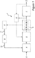
- Fig. 1 illustrates a switching power conversion system 1 in accordance with an embodiment of the invention where an analogue input 2 is clipped using feedback from a feedback loop from a duty cycle measurement.
- the switching power conversion system 1 may for example be used in an audio amplifier assembly.
- the input 2 then being an analogue audio signal and the output 3 being an amplified analogue audio signal.
- the system 1 includes a clipping arrangement comprising a clipper 4 at the analogue input 2, a feedback path from a switching power stage 6 to the clipper 4, where the signal path includes a duty cycle measuring unit 8.
- the duty cycle measuring unit 8 is configured to measure a duty cycle of an output signal (a PWM signal) from a pulse modulator, such as e.g. from the output of a pulse modulator 6a (e.g. output of a comparator in a COM-system) in the switching power stage 6. From the output signal of the pulse modulator 6a in the switching power stage 6, the duty cycle measuring unit 8 generates one or more measurement signal(s) 11. The measurement signal(s) 11 indicates that a duty cycle at the output of the comparator 6a is too high or too low.
- a clip level filter 9 receives the measurement signal(s) at an input and outputs a clipping voltage 12.
- the clipping voltage can be either positive or negative depending on the clip level filter; however a clipping voltage magnitude 12 may generally be used.
- This clipping voltage (magnitude) 12 is subsequently received at an input of the clipper 4, and the clipper 4 is configured to limit the analogue input signal in accordance with a clipping level (which depends on the clipping voltage 12).
- a lower clipping voltage magnitude generated/provided by the clip level filter results in a lower clipping level (i.e. the analogue input signal is clipped to a higher extent or alternatively the analogue input signal is more limited).
- the switching power conversion system 1 can further include a compensator 5, feedback signals and feedback filters (represented by the feedback block 10) for suppressing errors in the switching power stage 6 and the demodulation filter 7, and also to ensure self-oscillating conditions in COM-systems.
- the duty cycle is, as mentioned, measured at the output PWM (output of the pulse modulator 6a). However, in alternative implementations/embodiments the duty cycle of the output PWM can be measured at the output of the driver stage 6b, however the components used at the measuring block must be accordingly adjusted to withstand the higher voltage levels.
- the duty cycle level is compared to a threshold to find out if the duty cycle is too high or too low (i.e. if the modulation depth is too high).
- the duty cycle measuring block 8 together with the clip level filter 9 can lower the clipping level of the input signal until the duty cycle is not too high or too low (i.e. at an acceptable level). Similarly, the clipping level of the input signal can be increased if the duty cycle is not too high or too low.
- FIG. 2 displays a schematic circuit of an embodiment of the duty cycle measure block 200 (8 in Fig.1 ).
- the top block 202a (or sometimes called low side 202a) is configured to analyze if the duty cycle of the input (PWM) signal 201 is too low, i.e. if the time the PWM signal 201 is low is too long compared to the time the previous pulse was high.
- a capacitor 203a is set to an initial value of 0V.
- the capacitor 203a is set to the initial value of 0V by means of a switch 204a and a rising edge detection unit 205a which closes the switch 204a when a rising edge in the input signal 201 is detected, which consequently short circuits the capacitor 203a.
- the capacitor 203a when the input signal 201 is high the capacitor 203a is charged with a first current ( i*x ) by means of a first current source 206a, and when the input signal is low the capacitor 203a is discharged with a second current ( i ) by means of a second current source 207a.
- the second current being a predefined ratio/proportion of the first current, as indicated by the factor x. If the voltage across the capacitor 203a becomes lower than 0V (i.e. negative) the duty cycle of the input signal 201 is determined to be too low and the output signal 208a (measurement signal) from the top block 202a will be high as long as the voltage across the capacitor 203a is lower than 0V.
- the comparators 210 are referenced to ground, however they can also be referenced to a voltage in other embodiments.
- the top block 202a allows for very precise control of a minimum duty cycle level threshold value, and by increasing the charge current ( i*x ) (first current) relative to the discharge current ( i ) (second current), the lower the minimum duty cycle threshold value will be.
- the duty cycle of the input signal 201 must be above approximately 20 %, otherwise the top side 202a will produce a (high) signal at the output 208a, which indicates that the duty cycle is too low (or at least below 20 %).
- the bottom side 202b (or sometimes called the high side) of the block is configured to analyze if the duty cycle of the input signal 201 is too high.
- the bottom side 202b operates in an analogous manner as the top side but with an inverted input signal, as indicated by the inverter 209.
- the output signal 208a of the top side 202a will be high/positive if the duty cycle of the input signal 201 is too low
- the output signal 208b of the bottom side 202b will be high/positive if the duty cycle of the input signal 201 is too high.
- too high/too low is relative to a predefined value which is effectively controlled by controlling the ratio between the charging current (first current) and discharging current (second current), i.e. controlling the factor x.
- the factor x can be the same in both the top block 202a and the bottom block 202b in order to provide symmetrical duty cycle limits, e.g. if x is chosen to be 4 at both of the charging current sources 206a, 206b the duty cycle measurement block indicates if the duty cycle goes below or above 20% and 80 % respectively.
- the factor x could be chosen to be e.g. 3 or 5, then the duty cycle thresholds would be 25%, 75% and 16,7%, 83,3%, respectively, and so on.
- top and bottom block may be interchanged by adjusting the ratios of the charging and discharging currents and the circuit 200 may be configured so that the comparators generate an output 208a-b when the voltage across the capacitor 203a-b is above a predefined threshold voltage by having a set of falling edge detection units instead of the rising edge detection units 205a-b and adjusting the current sources 206a-b, 207a-b accordingly.
- the charging current sources 206a-b may be configured to charge during a low period and the discharging current sources 207a-b may be configured to discharge during a high period of the input signal.
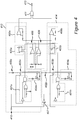
- FIG 3 shows a schematic circuit representation of an exemplary embodiment of a first order clip level filter 300 (9 in Fig. 1 ).
- the filter receives the two signals 208a, 208b from the duty cycle measure block (200 in Fig. 2 ) at an input.
- the filter 300 can also be utilized in systems having more than one channel as indicated by the additional inputs 208c-d.
- the operation of the clip level filter is in some ways similar to the operation of the two blocks in the duty cycle measuring unit (202a, 202b in Fig. 2 ) as there are clip filter current sources 303a-b which are charging and discharging a clip filter capacitor 302.
- a voltage across a capacitor 302 is used to control a clipping level of a signal applied at an amplifier input (2 in Fig. 1 ).
- the duty cycle measuring unit e.g. 200 in Fig. 2
- the two output signals (208a, 208b) from the duty cycle measuring unit are low and the capacitor 302 is charged with a first current ( i ) by means of a first current source 303a.
- the capacitor 302 is discharged with a second current ( ix ) by means of a second current source 303b, which lowers the voltage over the capacitor 302 and consequently the clipping voltage (at amplifier power conversion system input) can be lowered.
- the factor x which indicates the ratio between the currents of the two current sources is chosen to be 1. However, depending on the intended applications the factor x can be chosen to be higher or lower than 1, in order to e.g. more rapidly increase/decrease the clipping level voltage at the input (may be referred to as the filter's attack and release characteristics).
- x is chosen to be 1, i.e. the currents of the two clip filter current sources 303a, 303b are substantially of equal magnitude, will result in that: in order to change the clipping voltage 301 either one of the input signals 208a-d need to have a duty cycle of more than 50%.
- the duty cycle measure block 200 as discussed with reference to Fig 2 is configured to indicate if the duty cycle of an input PWM signal (201 in Fig. 2 ) is below or above 20% and 80% respectively, the resulting output 301 from the clip level filter 300 will maintain the duty cycle of the input PWM signal above or below 10% and 90% respectively.
- Fig. 4 is a circuit diagram of a duty cycle measuring unit in accordance with an exemplary embodiment of the invention.
- the circuit has been divided into separate section in order to facilitate the understanding of the functionality.
- Section 413 is configured to analyze if the duty cycle of the input 410 is too high.
- Section 414 is configured to analyze if the duty cycle of the input 410 is too low by inverting the input with the inverter 407.
- the outputs from the duty cycle high measure 413 and the duty cycle low measure 414 are combined with a gate 411 to the output 412, in order to produce a common measurement signal indicative of that the duty cycle is too high or too low.
- the circuit serves to show that the duty cycle clip level can be adjusted by controlling a factor between the charging current (first measurement current), which is generated by the first current generator/source 402a and 402b and the discharging current (second measurement current, which is generated by the second current generator/source 404a and 404b.
- first measurement current which is generated by the first current generator/source 402a and 402b
- second measurement current which is generated by the second current generator/source 404a and 404b.
- the charging current is always running and the discharging current is switched in with a switch 403a and 403b. Since the charge current is always running the discharging current must be larger to get a net discharging current.
- the blocks 401a and 401b are constructing a short pulse at a "falling edge" in order to short circuit the capacitor in 405a and 405b.
- Fig. 5 illustrates a circuit diagram of a first order clip level filter in accordance with an embodiment of the invention.
- the filter attack and release can be adjusted by controlling a factor which determines a ratio between the charging current (first clip filter current), generated by first clip filter current source 501, and the discharging current (second clip filter current) generated by the second clip filter current source 508.
- the discharging current may be chosen to be two times the charging current, if the charging current is always (i.e. continuously) running then the discharging current must be two times the charging current if the net charge of the clip filter capacitor 506 is to correspond to the scenario described earlier where the charging/discharging currents were the same but the charging current was only switched in for a certain time within a period of a PWM signal.
- the clip filter capacitor 506 can be pre-charged to the clip level set by the power supply rails; typically the pre-charge level is a level that is slightly higher than the clip level that the duty cycle clipper will produce/give.
- the release time is controlled by the charging current from the first clip filter current source 501 and the capacitor 506; the attack time is controlled by the capacitor 506 and a net discharging current (i.e. the discharging current minus the charging current that is always running).
- the input 509 is controlling the switch 507 which "switches in" the discharging current.
- the initial clip voltage 510 can be set by a factor of the positive supply voltage 504 or by a factor of the negative supply voltage 505.
- a comparator in section 502 is measuring if the duty cycle clipper level is lower than a predefined level and generating an output 511.
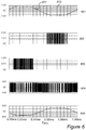
- Fig. 6 illustrates a set of graphs which are simulation results of a duty cycle clipper with a first order clip filter.
- the top plot/graph 601 (top in reference to the figure orientation) shows an input signal 611 of the power conversion system and a clipping signal 612. The clipping signal being the signal that is outputted by the clip level filter 9 in Fig. 1 .
- the second graph from the top 602 illustrates a signal that indicates that the duty cycle of an output PWM signal (illustrated in 604) is higher than a predefined threshold value.
- the middle graph 603 illustrates the corresponding signal that indicates that the duty cycle of the output PWM signal (illustrated in 604) is lower than a threshold value.
- the fourth graph 604 from the top is the PWM output signal
- the bottom graph 605 is the output signal of the audio amplifier assembly/switching power conversion system after the demodulation filter (e.g. 7 in Fig. 1 ).
- Fig. 7 is a zoomed in-view of the simulation plots/graphs in Fig. 6 in order to further elucidate the inventive concept.
- the graphs are arranged in the same order as in Fig. 6 where the top graph is the amplifier input signal and the clipping signal and the bottom graph is the amplifier output signal.
- the clipping signal 712 is lowered when one of the blocks in the duty cycle measuring unit (plot 702 and 703) generates an output which indicates that the duty cycle of the output PWM signal is above/below a threshold value.
- the signal in 703, that is indicating that the duty cycle is below the predefined threshold needs to have a duty cycle above 50% itself, i.e.
- the graph 702 shows the signal indicative of that the duty cycle of the PWM signal in 704 is above a predefined threshold and the bottom graph 705 shows the resulting output from an audio amplifier assembly comprising a system according to the invention.
- the clipping system according to the present invention can be implemented in various applications/systems as exemplified below, either in full or partly as components.
- the clipping system can accordingly be used systems where a single ended input signal is clipped and/or be used with systems where a balanced input signal is clipped.
- the clipping system can be implemented as a signal loop comprising a first order filter from duty cycle measurement to clipper, a higher order filter from duty cycle measurement to clipper or a multi step filter from duty cycle measurement to clipper.
- adjustable duty cycle measure circuit for level adjustment, adjustable duty cycle measure circuit by analog DC-voltage, adjustable duty cycle measure circuit by I2C (Inter-integrated circuit).
Landscapes
- Engineering & Computer Science (AREA)
- Power Engineering (AREA)
- Multimedia (AREA)
- Amplifiers (AREA)
Claims (13)
- Leistungsumwandlungssystem (1), Folgendes umfassend:einen Verstärkereingang (2) zum Erhalten eines analogen Eingangssignals;einen Verstärkerausgang (3) zum Bereitstellen eines Schaltausgangssignals;einen Begrenzer (4) zum Begrenzen des analogen Eingangssignals, um ein begrenztes Eingangssignal mit einem vordefinierten Bereich bereitzustellen, welcher durch einen Begrenzungspegel beschränkt ist;einen Pulsmodulator (6a) zum Modulieren des begrenzten Eingangssignals, um ein pulsbreitenmoduliertes (PWM-) Signal auszubilden;eine Schaltleistungsstufe (6) zur Verstärkung des PWM-Signals, um das Schaltausgangssignal auszubilden; undeinen Rückkopplungsweg zu dem Begrenzer, wobei der Rückkopplungsweg Folgendes umfasst:eine Tastverhältnis-Messeinheit (8, 200), welche konfiguriert ist, ein Tastverhältnis des PWM-Signals zu messen und ein Messsignal (11, 208a, 208b) zu erzeugen, welches das Tastverhältnis angibt; undeinen Begrenzungspegelfilter (9, 300), welcher konfiguriert ist, das Messsignal zu erhalten und eine Begrenzungsspannung (12) bereitzustellen;wobei der Begrenzer verbunden ist, die Begrenzungsspannung zu erhalten, und konfiguriert ist, den Begrenzungspegel auf der Grundlage der Begrenzungsspannung einzustellen.
- Leistungsumwandlungssystem (1) nach Anspruch 1, wobei der Rückkopplungsweg von einem Ausgang des Pulsmodulators (6a) ausgeht.
- Leistungsumwandlungssystem (1) nach Anspruch 1, wobei der Rückkopplungsweg von einem Ausgang der Leistungsstufe (6) ausgeht.
- Leistungsumwandlungssystem (1) nach einem der vorhergehenden Ansprüche, wobei die Tastverhältnis-Messeinheit (8, 200) einen tiefen Block (202a) und einen hohen Block (202b) umfasst, welche jeweils das PWM-Signal (201) als Eingang aufweisen, wobei jeder Block konfiguriert ist, zu messen, ob das Tastverhältnis des PWM-Signals unterhalb bzw. oberhalb eines vordefinierten Schwellenwerts liegt, wobei jeder Block Folgendes umfasst:eine erste Messstromquelle (206a, 206b), welche konfiguriert ist, einen Messkondensator (203a, 203b) mit einem ersten Messstrom (ix) während einer hohen oder einer tiefen Periode des PWM-Signals zu laden;eine zweite Messstromquelle (207a, 207b), welche konfiguriert ist, den Messkondensator (203a, 203b) mit einem zweiten Messstrom (i) während der anderen der hohen oder der tiefen Periode des PWM-Signals zu entladen;wobei der erste Messstrom ein vordefiniertes Verhältnis des zweiten Stroms ist; undeinen Messkomparator (210), welcher konfiguriert ist, das Messsignal (11, 208a, 208b) zu erzeugen, wenn eine Spannung über den Messkondensator über oder unter einer vordefinierten Messschwellenspannung liegt.
- Leistungsumwandlungssystem (1) nach einem der Ansprüche 1 bis 3, wobei die Tastverhältnis-Messeinheit (200) einen tiefen Block (202a) und einen hohen Block (202b) umfasst, welche jeweils das PWM-Signal (201) als Eingang aufweisen, wobei jeder Block konfiguriert ist, zu messen, ob das Tastverhältnis des PWM-Signals unterhalb bzw. oberhalb eines vordefinierten Schwellenwerts liegt, wobei jeder Block Folgendes umfasst:eine erste Messstromquelle (206a, 206b), welche konfiguriert ist, einen Messkondensator (203a, 203b) kontinuierlich mit einem ersten Messstrom (ix) zu laden;eine zweite Messstromquelle (207a, 207b), welche konfiguriert ist, den Messkondensator mit einem zweiten Messstrom (i) während einer hohen oder einer tiefen Periode des PWM-Signals zu entladen;wobei der erste Messstrom ein vordefiniertes Verhältnis des zweiten Stroms ist; undeinen Messkomparator (210), welcher konfiguriert ist, das Messsignal (11, 208a, 208b) zu erzeugen, wenn eine Spannung über den Messkondensator unter einer vordefinierten Messschwellenspannung liegt.
- Leistungsumwandlungssystem (1) nach einem der vorhergehenden Ansprüche, wobei der Begrenzungspegelfilter (9, 300) Folgendes umfasst:eine erste Begrenzungsfilter-Stromquelle (303a), welche konfiguriert ist, einen Begrenzungsfilterkondensator (302) mit einem ersten Begrenzungsfilterstrom während einer hohen oder einer tiefen Periode des Messsignals (208a, 208b, 208c, 208d) zu laden;eine zweite Begrenzungsfilter-Stromquelle (303b), welche konfiguriert ist, den Begrenzungsfilterkondensator (302) mit einem zweiten Begrenzungsfilterstrom während der anderen der hohen oder tiefen Periode des Messsignals (208a, 208b, 208c, 208d) zu entladen;wobei eine Spannung über den Begrenzungsfilterkondensator als die Begrenzungsspannung verwendet wird.
- Leistungsumwandlungssystem (1) nach einem der Ansprüche 1 bis 5, wobei der Begrenzungspegelfilter (9, 300) Folgendes umfasst:eine erste Begrenzungsfilter-Stromquelle (303a), welche konfiguriert ist, einen Begrenzungsfilterkondensator (302) kontinuierlich mit einem ersten Begrenzungsfilterstrom zu laden;eine zweite Begrenzungsfilter-Stromquelle (303b), welche konfiguriert ist, den Begrenzungsfilterkondensator mit einem zweiten Begrenzungsfilterstrom während einer hohen oder einer tiefen Periode des Messsignals (208a, 208b, 208c, 208d) zu entladen;wobei eine Spannung über den Begrenzungsfilterkondensator als die Begrenzungsspannung verwendet wird.
- Leistungsumwandlungssystem (1) nach Anspruch 6 oder 7, wobei der erste Begrenzungsfilterstrom ein vordefiniertes Verhältnis des zweiten Begrenzungsfilterstroms ist.
- Leistungsumwandlungssystem (1) nach Anspruch 6 oder 7, wobei der Begrenzungspegelfilter (9, 300) konfiguriert ist, Messsignale aus mehreren Kanälen zu erhalten.
- Leistungsumwandlungssystem (1) nach einem der vorhergehenden Ansprüche, wobei das analoge Eingangssignal ein Audiosignal ist.
- Leistungsumwandlungssystem (1) nach Anspruch 10, weiterhin umfassend einen Demodulationsfilter (7), um das Schaltausgangssignal aus der Schaltleistungsstufe (6) zu demodulieren, um ein verstärktes Audiosignal auszubilden.
- Leistungsumwandlungssystem (1) nach Anspruch 11, wobei der Rückkopplungsweg ein erster Rückkopplungsweg ist und wobei das Leistungsumwandlungssystem weiterhin Folgendes umfasst:einen Kompensator (5) zwischen dem Begrenzer und dem Pulsmodulator; undeinen zweiten Rückkopplungsweg, welcher von einem Ausgang des Demodulationsfilters (7) zu dem Kompensator (5) angelegt ist.
- Leistungsumwandlungssystem (1) nach Anspruch 12, weiterhin umfassend einen dritten Rückkopplungsweg von einem Ausgang der Schaltleistungsstufe (6) zu dem Kompensator (5).
Applications Claiming Priority (3)
| Application Number | Priority Date | Filing Date | Title |
|---|---|---|---|
| DKPA201500217 | 2015-04-09 | ||
| DKPA201500539 | 2015-06-22 | ||
| PCT/EP2016/054893 WO2016162156A1 (en) | 2015-04-09 | 2016-03-08 | Duty cycle clipper |
Publications (2)
| Publication Number | Publication Date |
|---|---|
| EP3281293A1 EP3281293A1 (de) | 2018-02-14 |
| EP3281293B1 true EP3281293B1 (de) | 2019-02-13 |
Family
ID=55485001
Family Applications (1)
| Application Number | Title | Priority Date | Filing Date |
|---|---|---|---|
| EP16708422.7A Active EP3281293B1 (de) | 2015-04-09 | 2016-03-08 | Tastverhältnisbegrenzer |
Country Status (3)
| Country | Link |
|---|---|
| US (1) | US10256780B2 (de) |
| EP (1) | EP3281293B1 (de) |
| WO (1) | WO2016162156A1 (de) |
Family Cites Families (6)
| Publication number | Priority date | Publication date | Assignee | Title |
|---|---|---|---|---|
| US4724396A (en) * | 1984-08-21 | 1988-02-09 | Peavey Electronics Corporation | Digital audio amplifier |
| US4600891A (en) * | 1984-08-21 | 1986-07-15 | Peavey Electronics Corporation | Digital audio amplifier having a high power output level and low distortion |
| WO2001091284A1 (en) | 2000-05-25 | 2001-11-29 | Koninklijke Philips Electronics N.V. | Pwm limiter |
| JP4617298B2 (ja) | 2003-03-21 | 2011-01-19 | ディー2オーディオ コーポレイション | クリップ検出と信号変調システム及び方法 |
| US7142050B2 (en) * | 2003-10-15 | 2006-11-28 | Texas Instruments Incorporated | Recovery from clipping events in a class D amplifier |
| US7315202B2 (en) | 2004-07-02 | 2008-01-01 | Yamaha Corporation | Pulse-width modulation amplifier and suppression of clipping therefor |
-
2016
- 2016-03-08 US US15/556,449 patent/US10256780B2/en active Active
- 2016-03-08 WO PCT/EP2016/054893 patent/WO2016162156A1/en not_active Ceased
- 2016-03-08 EP EP16708422.7A patent/EP3281293B1/de active Active
Also Published As
| Publication number | Publication date |
|---|---|
| EP3281293A1 (de) | 2018-02-14 |
| WO2016162156A1 (en) | 2016-10-13 |
| US20180054173A1 (en) | 2018-02-22 |
| US10256780B2 (en) | 2019-04-09 |
Similar Documents
| Publication | Publication Date | Title |
|---|---|---|
| US8040184B2 (en) | Class-D amplifier | |
| US7557622B2 (en) | Precision triangle waveform generator | |
| US8487690B2 (en) | Dual mode charge pump | |
| US7482870B2 (en) | Class D amplifier | |
| US8289075B2 (en) | Class-D amplifier | |
| US20170054422A1 (en) | Reduced crosstalk and matched output power audio amplifier using a triangle wave generator | |
| US11240606B2 (en) | Amplifiers for parametric loudspeakers | |
| JP2016127422A (ja) | 増幅回路及びこれを有する電流センサ | |
| EP2802074B1 (de) | Verstärkerschaltung und Verstärkungsverfahren | |
| US7372324B2 (en) | Digital amplifier | |
| EP3079256A1 (de) | Nullpunktabweichung, uneingeschränkte und einstellbare referenzspannungserzeugung | |
| US9385694B2 (en) | Low-power programmable oscillator and ramp generator | |
| US20140233685A1 (en) | Receiver compensation | |
| EP3281293B1 (de) | Tastverhältnisbegrenzer | |
| JP5343782B2 (ja) | D級増幅器 | |
| US9825600B2 (en) | Class D amplifier and electronic devices including the same | |
| US10910952B1 (en) | Control apparatus and method for current resonance circuit and current resonance power supply | |
| JPH10177043A (ja) | Whパルス検出回路 | |
| JPH04280170A (ja) | 受像管駆動回路 | |
| JPH02303209A (ja) | 多段出力制御装置 | |
| JPS6359214A (ja) | パルス幅変調回路 | |
| JPS62199106A (ja) | 時定数ミユ−ト回路 |
Legal Events
| Date | Code | Title | Description |
|---|---|---|---|
| STAA | Information on the status of an ep patent application or granted ep patent |
Free format text: STATUS: THE INTERNATIONAL PUBLICATION HAS BEEN MADE |
|
| PUAI | Public reference made under article 153(3) epc to a published international application that has entered the european phase |
Free format text: ORIGINAL CODE: 0009012 |
|
| STAA | Information on the status of an ep patent application or granted ep patent |
Free format text: STATUS: REQUEST FOR EXAMINATION WAS MADE |
|
| 17P | Request for examination filed |
Effective date: 20171024 |
|
| AK | Designated contracting states |
Kind code of ref document: A1 Designated state(s): AL AT BE BG CH CY CZ DE DK EE ES FI FR GB GR HR HU IE IS IT LI LT LU LV MC MK MT NL NO PL PT RO RS SE SI SK SM TR |
|
| AX | Request for extension of the european patent |
Extension state: BA ME |
|
| DAV | Request for validation of the european patent (deleted) | ||
| DAX | Request for extension of the european patent (deleted) | ||
| REG | Reference to a national code |
Ref country code: DE Ref legal event code: R079 Ref document number: 602016009933 Country of ref document: DE Free format text: PREVIOUS MAIN CLASS: H03F0003181000 Ipc: H03F0001520000 |
|
| GRAJ | Information related to disapproval of communication of intention to grant by the applicant or resumption of examination proceedings by the epo deleted |
Free format text: ORIGINAL CODE: EPIDOSDIGR1 |
|
| STAA | Information on the status of an ep patent application or granted ep patent |
Free format text: STATUS: GRANT OF PATENT IS INTENDED |
|
| GRAP | Despatch of communication of intention to grant a patent |
Free format text: ORIGINAL CODE: EPIDOSNIGR1 |
|
| RIC1 | Information provided on ipc code assigned before grant |
Ipc: H03F 1/52 20060101AFI20180910BHEP Ipc: H03F 3/217 20060101ALI20180910BHEP Ipc: H03F 3/181 20060101ALI20180910BHEP |
|
| INTG | Intention to grant announced |
Effective date: 20181005 |
|
| GRAS | Grant fee paid |
Free format text: ORIGINAL CODE: EPIDOSNIGR3 |
|
| GRAA | (expected) grant |
Free format text: ORIGINAL CODE: 0009210 |
|
| STAA | Information on the status of an ep patent application or granted ep patent |
Free format text: STATUS: THE PATENT HAS BEEN GRANTED |
|
| AK | Designated contracting states |
Kind code of ref document: B1 Designated state(s): AL AT BE BG CH CY CZ DE DK EE ES FI FR GB GR HR HU IE IS IT LI LT LU LV MC MK MT NL NO PL PT RO RS SE SI SK SM TR |
|
| REG | Reference to a national code |
Ref country code: GB Ref legal event code: FG4D |
|
| REG | Reference to a national code |
Ref country code: CH Ref legal event code: EP Ref country code: AT Ref legal event code: REF Ref document number: 1096802 Country of ref document: AT Kind code of ref document: T Effective date: 20190215 |
|
| REG | Reference to a national code |
Ref country code: IE Ref legal event code: FG4D |
|
| REG | Reference to a national code |
Ref country code: DE Ref legal event code: R096 Ref document number: 602016009933 Country of ref document: DE |
|
| REG | Reference to a national code |
Ref country code: LT Ref legal event code: MG4D |
|
| REG | Reference to a national code |
Ref country code: NL Ref legal event code: MP Effective date: 20190213 |
|
| PG25 | Lapsed in a contracting state [announced via postgrant information from national office to epo] |
Ref country code: NO Free format text: LAPSE BECAUSE OF FAILURE TO SUBMIT A TRANSLATION OF THE DESCRIPTION OR TO PAY THE FEE WITHIN THE PRESCRIBED TIME-LIMIT Effective date: 20190513 Ref country code: LT Free format text: LAPSE BECAUSE OF FAILURE TO SUBMIT A TRANSLATION OF THE DESCRIPTION OR TO PAY THE FEE WITHIN THE PRESCRIBED TIME-LIMIT Effective date: 20190213 Ref country code: NL Free format text: LAPSE BECAUSE OF FAILURE TO SUBMIT A TRANSLATION OF THE DESCRIPTION OR TO PAY THE FEE WITHIN THE PRESCRIBED TIME-LIMIT Effective date: 20190213 Ref country code: SE Free format text: LAPSE BECAUSE OF FAILURE TO SUBMIT A TRANSLATION OF THE DESCRIPTION OR TO PAY THE FEE WITHIN THE PRESCRIBED TIME-LIMIT Effective date: 20190213 Ref country code: PT Free format text: LAPSE BECAUSE OF FAILURE TO SUBMIT A TRANSLATION OF THE DESCRIPTION OR TO PAY THE FEE WITHIN THE PRESCRIBED TIME-LIMIT Effective date: 20190613 Ref country code: FI Free format text: LAPSE BECAUSE OF FAILURE TO SUBMIT A TRANSLATION OF THE DESCRIPTION OR TO PAY THE FEE WITHIN THE PRESCRIBED TIME-LIMIT Effective date: 20190213 |
|
| PG25 | Lapsed in a contracting state [announced via postgrant information from national office to epo] |
Ref country code: LV Free format text: LAPSE BECAUSE OF FAILURE TO SUBMIT A TRANSLATION OF THE DESCRIPTION OR TO PAY THE FEE WITHIN THE PRESCRIBED TIME-LIMIT Effective date: 20190213 Ref country code: HR Free format text: LAPSE BECAUSE OF FAILURE TO SUBMIT A TRANSLATION OF THE DESCRIPTION OR TO PAY THE FEE WITHIN THE PRESCRIBED TIME-LIMIT Effective date: 20190213 Ref country code: RS Free format text: LAPSE BECAUSE OF FAILURE TO SUBMIT A TRANSLATION OF THE DESCRIPTION OR TO PAY THE FEE WITHIN THE PRESCRIBED TIME-LIMIT Effective date: 20190213 Ref country code: BG Free format text: LAPSE BECAUSE OF FAILURE TO SUBMIT A TRANSLATION OF THE DESCRIPTION OR TO PAY THE FEE WITHIN THE PRESCRIBED TIME-LIMIT Effective date: 20190513 Ref country code: IS Free format text: LAPSE BECAUSE OF FAILURE TO SUBMIT A TRANSLATION OF THE DESCRIPTION OR TO PAY THE FEE WITHIN THE PRESCRIBED TIME-LIMIT Effective date: 20190613 Ref country code: GR Free format text: LAPSE BECAUSE OF FAILURE TO SUBMIT A TRANSLATION OF THE DESCRIPTION OR TO PAY THE FEE WITHIN THE PRESCRIBED TIME-LIMIT Effective date: 20190514 |
|
| REG | Reference to a national code |
Ref country code: AT Ref legal event code: MK05 Ref document number: 1096802 Country of ref document: AT Kind code of ref document: T Effective date: 20190213 |
|
| PG25 | Lapsed in a contracting state [announced via postgrant information from national office to epo] |
Ref country code: DK Free format text: LAPSE BECAUSE OF FAILURE TO SUBMIT A TRANSLATION OF THE DESCRIPTION OR TO PAY THE FEE WITHIN THE PRESCRIBED TIME-LIMIT Effective date: 20190213 Ref country code: ES Free format text: LAPSE BECAUSE OF FAILURE TO SUBMIT A TRANSLATION OF THE DESCRIPTION OR TO PAY THE FEE WITHIN THE PRESCRIBED TIME-LIMIT Effective date: 20190213 Ref country code: AL Free format text: LAPSE BECAUSE OF FAILURE TO SUBMIT A TRANSLATION OF THE DESCRIPTION OR TO PAY THE FEE WITHIN THE PRESCRIBED TIME-LIMIT Effective date: 20190213 Ref country code: SK Free format text: LAPSE BECAUSE OF FAILURE TO SUBMIT A TRANSLATION OF THE DESCRIPTION OR TO PAY THE FEE WITHIN THE PRESCRIBED TIME-LIMIT Effective date: 20190213 Ref country code: CZ Free format text: LAPSE BECAUSE OF FAILURE TO SUBMIT A TRANSLATION OF THE DESCRIPTION OR TO PAY THE FEE WITHIN THE PRESCRIBED TIME-LIMIT Effective date: 20190213 Ref country code: RO Free format text: LAPSE BECAUSE OF FAILURE TO SUBMIT A TRANSLATION OF THE DESCRIPTION OR TO PAY THE FEE WITHIN THE PRESCRIBED TIME-LIMIT Effective date: 20190213 Ref country code: IT Free format text: LAPSE BECAUSE OF FAILURE TO SUBMIT A TRANSLATION OF THE DESCRIPTION OR TO PAY THE FEE WITHIN THE PRESCRIBED TIME-LIMIT Effective date: 20190213 Ref country code: EE Free format text: LAPSE BECAUSE OF FAILURE TO SUBMIT A TRANSLATION OF THE DESCRIPTION OR TO PAY THE FEE WITHIN THE PRESCRIBED TIME-LIMIT Effective date: 20190213 |
|
| REG | Reference to a national code |
Ref country code: CH Ref legal event code: PL |
|
| REG | Reference to a national code |
Ref country code: DE Ref legal event code: R097 Ref document number: 602016009933 Country of ref document: DE |
|
| PG25 | Lapsed in a contracting state [announced via postgrant information from national office to epo] |
Ref country code: SM Free format text: LAPSE BECAUSE OF FAILURE TO SUBMIT A TRANSLATION OF THE DESCRIPTION OR TO PAY THE FEE WITHIN THE PRESCRIBED TIME-LIMIT Effective date: 20190213 Ref country code: LU Free format text: LAPSE BECAUSE OF NON-PAYMENT OF DUE FEES Effective date: 20190308 Ref country code: PL Free format text: LAPSE BECAUSE OF FAILURE TO SUBMIT A TRANSLATION OF THE DESCRIPTION OR TO PAY THE FEE WITHIN THE PRESCRIBED TIME-LIMIT Effective date: 20190213 |
|
| REG | Reference to a national code |
Ref country code: BE Ref legal event code: MM Effective date: 20190331 |
|
| PLBE | No opposition filed within time limit |
Free format text: ORIGINAL CODE: 0009261 |
|
| STAA | Information on the status of an ep patent application or granted ep patent |
Free format text: STATUS: NO OPPOSITION FILED WITHIN TIME LIMIT |
|
| PG25 | Lapsed in a contracting state [announced via postgrant information from national office to epo] |
Ref country code: MC Free format text: LAPSE BECAUSE OF FAILURE TO SUBMIT A TRANSLATION OF THE DESCRIPTION OR TO PAY THE FEE WITHIN THE PRESCRIBED TIME-LIMIT Effective date: 20190213 Ref country code: AT Free format text: LAPSE BECAUSE OF FAILURE TO SUBMIT A TRANSLATION OF THE DESCRIPTION OR TO PAY THE FEE WITHIN THE PRESCRIBED TIME-LIMIT Effective date: 20190213 |
|
| 26N | No opposition filed |
Effective date: 20191114 |
|
| PG25 | Lapsed in a contracting state [announced via postgrant information from national office to epo] |
Ref country code: CH Free format text: LAPSE BECAUSE OF NON-PAYMENT OF DUE FEES Effective date: 20190331 Ref country code: LI Free format text: LAPSE BECAUSE OF NON-PAYMENT OF DUE FEES Effective date: 20190331 Ref country code: IE Free format text: LAPSE BECAUSE OF NON-PAYMENT OF DUE FEES Effective date: 20190308 |
|
| PG25 | Lapsed in a contracting state [announced via postgrant information from national office to epo] |
Ref country code: BE Free format text: LAPSE BECAUSE OF NON-PAYMENT OF DUE FEES Effective date: 20190331 Ref country code: SI Free format text: LAPSE BECAUSE OF FAILURE TO SUBMIT A TRANSLATION OF THE DESCRIPTION OR TO PAY THE FEE WITHIN THE PRESCRIBED TIME-LIMIT Effective date: 20190213 |
|
| PG25 | Lapsed in a contracting state [announced via postgrant information from national office to epo] |
Ref country code: TR Free format text: LAPSE BECAUSE OF FAILURE TO SUBMIT A TRANSLATION OF THE DESCRIPTION OR TO PAY THE FEE WITHIN THE PRESCRIBED TIME-LIMIT Effective date: 20190213 |
|
| PG25 | Lapsed in a contracting state [announced via postgrant information from national office to epo] |
Ref country code: MT Free format text: LAPSE BECAUSE OF NON-PAYMENT OF DUE FEES Effective date: 20190308 |
|
| PG25 | Lapsed in a contracting state [announced via postgrant information from national office to epo] |
Ref country code: CY Free format text: LAPSE BECAUSE OF FAILURE TO SUBMIT A TRANSLATION OF THE DESCRIPTION OR TO PAY THE FEE WITHIN THE PRESCRIBED TIME-LIMIT Effective date: 20190213 |
|
| PG25 | Lapsed in a contracting state [announced via postgrant information from national office to epo] |
Ref country code: HU Free format text: LAPSE BECAUSE OF FAILURE TO SUBMIT A TRANSLATION OF THE DESCRIPTION OR TO PAY THE FEE WITHIN THE PRESCRIBED TIME-LIMIT; INVALID AB INITIO Effective date: 20160308 |
|
| PG25 | Lapsed in a contracting state [announced via postgrant information from national office to epo] |
Ref country code: MK Free format text: LAPSE BECAUSE OF FAILURE TO SUBMIT A TRANSLATION OF THE DESCRIPTION OR TO PAY THE FEE WITHIN THE PRESCRIBED TIME-LIMIT Effective date: 20190213 |
|
| P01 | Opt-out of the competence of the unified patent court (upc) registered |
Effective date: 20230523 |
|
| PGFP | Annual fee paid to national office [announced via postgrant information from national office to epo] |
Ref country code: DE Payment date: 20250312 Year of fee payment: 10 |
|
| PGFP | Annual fee paid to national office [announced via postgrant information from national office to epo] |
Ref country code: FR Payment date: 20250217 Year of fee payment: 10 |
|
| PGFP | Annual fee paid to national office [announced via postgrant information from national office to epo] |
Ref country code: GB Payment date: 20250310 Year of fee payment: 10 |