EP3278326B1 - Virtuelle grenzenlose anzeige - Google Patents
Virtuelle grenzenlose anzeige Download PDFInfo
- Publication number
- EP3278326B1 EP3278326B1 EP15781216.5A EP15781216A EP3278326B1 EP 3278326 B1 EP3278326 B1 EP 3278326B1 EP 15781216 A EP15781216 A EP 15781216A EP 3278326 B1 EP3278326 B1 EP 3278326B1
- Authority
- EP
- European Patent Office
- Prior art keywords
- display
- layer
- display panel
- panel
- driver
- Prior art date
- Legal status (The legal status is an assumption and is not a legal conclusion. Google has not performed a legal analysis and makes no representation as to the accuracy of the status listed.)
- Active
Links
Images








Classifications
-
- G—PHYSICS
- G02—OPTICS
- G02F—OPTICAL DEVICES OR ARRANGEMENTS FOR THE CONTROL OF LIGHT BY MODIFICATION OF THE OPTICAL PROPERTIES OF THE MEDIA OF THE ELEMENTS INVOLVED THEREIN; NON-LINEAR OPTICS; FREQUENCY-CHANGING OF LIGHT; OPTICAL LOGIC ELEMENTS; OPTICAL ANALOGUE/DIGITAL CONVERTERS
- G02F1/00—Devices or arrangements for the control of the intensity, colour, phase, polarisation or direction of light arriving from an independent light source, e.g. switching, gating or modulating; Non-linear optics
- G02F1/01—Devices or arrangements for the control of the intensity, colour, phase, polarisation or direction of light arriving from an independent light source, e.g. switching, gating or modulating; Non-linear optics for the control of the intensity, phase, polarisation or colour
- G02F1/13—Devices or arrangements for the control of the intensity, colour, phase, polarisation or direction of light arriving from an independent light source, e.g. switching, gating or modulating; Non-linear optics for the control of the intensity, phase, polarisation or colour based on liquid crystals, e.g. single liquid crystal display cells
- G02F1/133—Constructional arrangements; Operation of liquid crystal cells; Circuit arrangements
- G02F1/1333—Constructional arrangements; Manufacturing methods
- G02F1/13338—Input devices, e.g. touch panels
-
- G—PHYSICS
- G02—OPTICS
- G02F—OPTICAL DEVICES OR ARRANGEMENTS FOR THE CONTROL OF LIGHT BY MODIFICATION OF THE OPTICAL PROPERTIES OF THE MEDIA OF THE ELEMENTS INVOLVED THEREIN; NON-LINEAR OPTICS; FREQUENCY-CHANGING OF LIGHT; OPTICAL LOGIC ELEMENTS; OPTICAL ANALOGUE/DIGITAL CONVERTERS
- G02F1/00—Devices or arrangements for the control of the intensity, colour, phase, polarisation or direction of light arriving from an independent light source, e.g. switching, gating or modulating; Non-linear optics
- G02F1/01—Devices or arrangements for the control of the intensity, colour, phase, polarisation or direction of light arriving from an independent light source, e.g. switching, gating or modulating; Non-linear optics for the control of the intensity, phase, polarisation or colour
- G02F1/13—Devices or arrangements for the control of the intensity, colour, phase, polarisation or direction of light arriving from an independent light source, e.g. switching, gating or modulating; Non-linear optics for the control of the intensity, phase, polarisation or colour based on liquid crystals, e.g. single liquid crystal display cells
- G02F1/133—Constructional arrangements; Operation of liquid crystal cells; Circuit arrangements
- G02F1/1333—Constructional arrangements; Manufacturing methods
- G02F1/1345—Conductors connecting electrodes to cell terminals
- G02F1/13452—Conductors connecting driver circuitry and terminals of panels
-
- G—PHYSICS
- G04—HOROLOGY
- G04G—ELECTRONIC TIME-PIECES
- G04G17/00—Structural details; Housings
- G04G17/02—Component assemblies
- G04G17/04—Mounting of electronic components
- G04G17/045—Mounting of the display
-
- G—PHYSICS
- G04—HOROLOGY
- G04G—ELECTRONIC TIME-PIECES
- G04G17/00—Structural details; Housings
- G04G17/02—Component assemblies
- G04G17/06—Electric connectors, e.g. conductive elastomers
-
- G—PHYSICS
- G04—HOROLOGY
- G04G—ELECTRONIC TIME-PIECES
- G04G21/00—Input or output devices integrated in time-pieces
- G04G21/08—Touch switches specially adapted for time-pieces
-
- G—PHYSICS
- G06—COMPUTING OR CALCULATING; COUNTING
- G06F—ELECTRIC DIGITAL DATA PROCESSING
- G06F3/00—Input arrangements for transferring data to be processed into a form capable of being handled by the computer; Output arrangements for transferring data from processing unit to output unit, e.g. interface arrangements
- G06F3/01—Input arrangements or combined input and output arrangements for interaction between user and computer
- G06F3/03—Arrangements for converting the position or the displacement of a member into a coded form
- G06F3/041—Digitisers, e.g. for touch screens or touch pads, characterised by the transducing means
-
- G—PHYSICS
- G09—EDUCATION; CRYPTOGRAPHY; DISPLAY; ADVERTISING; SEALS
- G09F—DISPLAYING; ADVERTISING; SIGNS; LABELS OR NAME-PLATES; SEALS
- G09F9/00—Indicating arrangements for variable information in which the information is built-up on a support by selection or combination of individual elements
- G09F9/30—Indicating arrangements for variable information in which the information is built-up on a support by selection or combination of individual elements in which the desired character or characters are formed by combining individual elements
-
- G—PHYSICS
- G06—COMPUTING OR CALCULATING; COUNTING
- G06F—ELECTRIC DIGITAL DATA PROCESSING
- G06F2203/00—Indexing scheme relating to G06F3/00 - G06F3/048
- G06F2203/041—Indexing scheme relating to G06F3/041 - G06F3/045
- G06F2203/04102—Flexible digitiser, i.e. constructional details for allowing the whole digitising part of a device to be flexed or rolled like a sheet of paper
-
- G—PHYSICS
- G06—COMPUTING OR CALCULATING; COUNTING
- G06F—ELECTRIC DIGITAL DATA PROCESSING
- G06F3/00—Input arrangements for transferring data to be processed into a form capable of being handled by the computer; Output arrangements for transferring data from processing unit to output unit, e.g. interface arrangements
- G06F3/01—Input arrangements or combined input and output arrangements for interaction between user and computer
- G06F3/03—Arrangements for converting the position or the displacement of a member into a coded form
- G06F3/041—Digitisers, e.g. for touch screens or touch pads, characterised by the transducing means
- G06F3/0412—Digitisers structurally integrated in a display
-
- H—ELECTRICITY
- H05—ELECTRIC TECHNIQUES NOT OTHERWISE PROVIDED FOR
- H05K—PRINTED CIRCUITS; CASINGS OR CONSTRUCTIONAL DETAILS OF ELECTRIC APPARATUS; MANUFACTURE OF ASSEMBLAGES OF ELECTRICAL COMPONENTS
- H05K1/00—Printed circuits
- H05K1/02—Details
- H05K1/14—Structural association of two or more printed circuits
- H05K1/147—Structural association of two or more printed circuits at least one of the printed circuits being bent or folded, e.g. by using a flexible printed circuit
-
- H—ELECTRICITY
- H05—ELECTRIC TECHNIQUES NOT OTHERWISE PROVIDED FOR
- H05K—PRINTED CIRCUITS; CASINGS OR CONSTRUCTIONAL DETAILS OF ELECTRIC APPARATUS; MANUFACTURE OF ASSEMBLAGES OF ELECTRICAL COMPONENTS
- H05K2201/00—Indexing scheme relating to printed circuits covered by H05K1/00
- H05K2201/10—Details of components or other objects attached to or integrated in a printed circuit board
- H05K2201/10007—Types of components
- H05K2201/10128—Display
Definitions
- a device such as a mobile device or a wearable device, offers various services to its user. Users may interact with the displays of these devices via touch panels and/or touchless panels. While touch and touchless input technologies allow users a great deal of flexibility when operating these devices, designers and manufacturers are continually striving to improve the qualities of the displays.
- US 2010/134743 A1 discloses a display comprising: a display panel (see e.g. figures 1 and 3 ), wherein the display panel comprises two or more bonding areas; a driver (810) configured to drive the display panel (220); a layer (control board 800) that provides a medium via which signals can propagate to and from the driver, and wherein the driver is mounted to the layer; and two or more flexible connectors (410, 510, 610, 710), characterized in that: the two or more flexible connectors (provide communication paths between the display panel and the driver, and a first end of each of the two or more flexible connectors connects to the display panel at a corresponding one of the two or more bonding areas, and a second end of each of the two or more flexible connectors connects to the driver via the layer.
- a configuration for a display which may be a touch display and/or a touchless display (simply referred to herein as "display”), can limit the possibilities of shape and/or size of certain components of the display.
- an active area of the display may be restricted in terms of shape and available size in view of the configuration and/or architecture of the display.
- Fig. 1A illustrates an exemplary display configuration 100 of various components of a display.
- display configuration 100 comprises a front window 110, a touch panel 115, a display active area 120, a color filter (CF) glass 125, a display driver 130, a display flexible printed circuit (FPC) 135, a touch flexible printed circuit (FPC) 140, a bonding area 141, and a thin-film transistor (TFT) glass 145.
- CF color filter
- FPC display flexible printed circuit
- FPC touch flexible printed circuit
- TFT thin-film transistor
- display active area 120 is limited in terms of shape and/or size since a space 147 is needed for display driver 130 and bonding area 141, which bonds display FPC 135 to thin-film transistor (TFT) glass 145. In this way, display signals are routed to a dedicated display driver area.
- the allocated space 147 for these components e.g., display driver 130, bonding area 141, etc.
- Fig. 1B illustrates a top-side view of an exemplary display 148 in which an area 149 is designed to place a display driver and a display flexible printed circuit for connection with the display driver (not illustrated).
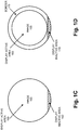
- Fig. 1C illustrates a top-side view of an exemplary display.
- a display active area 150 is limited due to a display inactive area 160 (e.g., where display driver 130, etc. resides).
- an image 155 displayed within display active area 150 has a non-circular active area.
- Fig. 1D illustrates a top-side view of another exemplary display.
- a display active area 165 is reduced (relative to display active area 150 of Fig. 1C ) to allow for a display inactive area 170 (e.g., where display driver 130, etc. resides).
- a border 175 serves as a disguise (from a user's perspective) for display inactive area 170 and provides a (smaller) circular display active area 165.
- a display configuration increases an area of display active area for use relative to a total area of the display active area.
- a driver is mounted to or situated on a system and not a display panel.
- the driver is mounted to or situated on a backside or underside of the system.
- the driver is connected to the system.
- the driver comprises a display driver.
- the driver comprises a display driver and a touch driver.
- the system comprises a substrate or a layer of material which allows signals to propagate.
- multiple flexible connectors may connect to the display panel and the system.
- the system routes signals to and/or from the multiple flexible connectors and to and/or from the driver (e.g., a display driver).
- the driver e.g., a display driver
- one or multiple flexible connectors may connect to a touch panel and the system.
- the system routes signals to and/or from the one or multiple flexible connectors and to and/or from the driver (e.g., a touch driver).
- the system routes signals to and/or from a host printed circuit board.
- the system may be a driver glass (e.g., glass panel, chip-on-glass, etc.), a flexible printed circuit (FPC), a chip-on-flex, a printed circuit board (PCB), or other type of substrate that allows the propagation of signals.
- a driver glass e.g., glass panel, chip-on-glass, etc.
- FPC flexible printed circuit
- PCB printed circuit board
- the display panel may be a liquid crystal display (LCD).
- the display panel may be implemented using other display technologies, such as, for example, color super twisted nematic (CSTN), thin film diode (TFD), organic light-emitting diode (OLED), active-matrix OLED (AMOLED), or some other conventional or known display technology (e.g., an electrophoretic display, etc.).
- CSTN color super twisted nematic
- TFD thin film diode
- OLED organic light-emitting diode
- AMOLED active-matrix OLED
- some other conventional or known display technology e.g., an electrophoretic display, etc.
- the display panel provides multiple bonding areas to permit multiple connections between the display panel and the multiple flexible connectors.
- the display panel comprises a step configuration in which a step portion of the display panel is used to provide the multiple bonding areas.
- the multiple flexible connectors connect to the display panel at the multiple bonding areas and wrap towards the system to which the driver is connected.
- one or multiple flexible connectors connect a touch panel, a touchless panel, or a touch and touchless panel (hereinafter simply referred to as a "touch panel").
- the touch panel provides one or multiple bonding areas to permit the connection(s).
- the touch flexible connector also wraps toward the system to which the driver is connected.
- Fig. 2A illustrates a cross-sectional view a display configuration 200 in which exemplary embodiments of a virtual borderless display may be implemented.
- display configuration 200 of a display comprises a front window 205, a touch panel 210, a display active area 215, a display 220, a backlight 225, a system 230, a driver 235, a touch FPC 240, and a display FPC 245.
- display configuration 200 may include additional components or layers, fewer components or layers, different components or layers, and/or a different arrangement of components or layers.
- display configuration 200 may not include touch panel 210 and touch FPC 240. Additionally, or alternatively, display configuration 200 may not include backlight 225.
- display configuration 200 may include additional components or layers, such as a polarizer, etc.
- Fig. 2A illustrates a single display FPC 240, as illustrated in other figures and described further below, display configuration 200 comprises multiple display FPCs 240.
- Front window 205 comprises a transparent layer of display configuration 200 through which a user may see visual elements (e.g., graphics, etc.) that are displayed.
- front window 205 may act as a protective covering.
- front window 205 may be oil resistant (e.g., oil on a human's finger), scratch or abrasion resistant, etc.
- Front window 205 may be implemented as a film or coating.
- front window 205 may be implemented as tempered glass or a plastic layer.
- Touch panel 210 comprises a device that senses the touch of a user and/or an instrument (e.g., a stylus, gloved touch, etc.). Touch panel may use one or multiple sensing technologies, such as, for example, capacitive sensing (e.g., resistive, projected, etc.), surface acoustic wave (SAW) sensing, resistive sensing, optical sensing, pressure sensing, infrared sensing, acoustic sensing, and/or gesture sensing. Touch panel 210 may detect a single-point input, a multipoint input, etc. Additionally, or alternatively, touch panel 210 comprises a device that senses air-touch and air-gestures of the user and/or an instrument. In this regard, touch panel 210 may be operable in an on-touch and/or touchless mode.
- capacitive sensing e.g., resistive, projected, etc.
- SAW surface acoustic wave
- resistive sensing e.g., optical sensing
- Display active area 215 comprises a portion of the total display area occupied by pixels.
- Display 220 comprises a display.
- display 220 may be implemented as a liquid crystal display (LCD), a plasma display panel (PDP), a field emission display (FED), or some other type of display technology (e.g., organic light-emitting diode (OLED), active matrix OLED (AMOLED), an electrophoretic display, etc).
- Display 220 can present to a user various types of graphics, such as displaying text, pictures, video, and various images (e.g., icons, objects, etc.).
- Backlight 225 comprises a device that produces light.
- a display such as an LCD may require backlight 225.
- backlight 225 is an optional component of display configuration 200.
- display configuration 200 may not comprise backlight 225.
- System 230 comprises a medium via which signals may propagate.
- the signals may include display signals, touch signals, control signals, power supply signals, or other types of signals that may contribute to the operation of a component included in display configuration 200.
- System 230 may also comprise other forms of components.
- system 230 may comprise a processor, an analog-to-digital converter, a microchip to enable communication with a main processing system, etc.
- system 230 may be implemented as a flexible printed circuit, a chip-on-flex, a glass panel (e.g., a driver glass, a chip-on-glass, etc.), a printed circuit board, or other type of substrate that allows the propagation of signals.
- system 230 connects to driver 235.
- system 230 connects to touch FPC 240, which in turn connects to touch panel 210. Additionally, according to an exemplary embodiment, system 230 connects to display FPC 245, which in turn connects to display 220. Based on these connections, system 230 enables correct routing of all signals from touch FPC 240 and display FPC 245 to driver 235. According to an exemplary embodiment, system 230 connects to a host printed circuit board (e.g., a main processing system of a user device) (not illustrated).
- a host printed circuit board e.g., a main processing system of a user device
- Driver 235 comprises a display driver or a display driver and a touch driver.
- driver 235 may comprise a register-based microprocessor.
- the display driver drives display 220 and the touch driver drives touch panel 210.
- Touch FPC 240 carries touch signals from touch panel 210 to driver 235.
- Display FPC 245 carries display signals from display 220 to driver 235.
- display FPC 245 may be a flexible printed circuit, a chip-on-flex, a chip-on-foil, or some other flexible material that can propagate signals. Touch FPC 240 may be implemented in a similar manner.
- a bonding area 247 connects display FPC 245 to display 220.
- a connection between display 220 and display FPC 245 may be implemented by way of heat sealing display FPC 245 to display 220 at bonding area 247.
- epoxy glue may be added between display FPC 245 and display 220 to provide reliability (e.g., so display FPC 245 is adhered securely).
- bonding area 247 provides a connection between display FPC 245 and display 220 and permits signals to be routed.
- driver 235 is mounted to the backside or underside of system 230. As a result, display active area 215 is less restricted in terms of size and/or shape since driver 235 is not mounted on display 220 and, as described further below, multiple display FPCs 245 may be used to route display signals to driver 235.
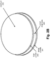
- Fig. 2B illustrates an elevational view of an exemplary display 220.
- display 220 has a circular configuration comprising a base layer 221 and a top layer 222.
- base layer 221 may comprise a TFT layer and top layer 222 may comprise a color filter layer.
- base layer 221 may comprise a TFT layer
- top layer 222 may comprise an encapsulation layer.
- base layer 221 may comprise a TFT layer and top layer 222 may comprise an encapsulation layer.
- the exemplary display technologies described above such as LCD, OLED, electrophoretic, etc., may include additional layers, different layers, and/or a different arrangement of layers than those specifically described herein.
- base layer 221 has a larger circular shape than top layer 222, a step portion 223 is formed.
- step portion 223 is present around the entire perimeter.
- display 220 may have a different configuration, such as elliptical, square, rectangular, triangular, or other type of three-dimensional shape. Additionally, or alternatively, display 220 may comprise another type of configuration that provides a similarly functioning bonding area 247.
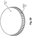
- Figs. 2C and 2D illustrate elevational views of an exemplary configuration of display 220 and display FPCs 245 connections.
- display FPC 245-1 through display FPC 245-8 also referred to collectively as display FPCs 245 and generally or individually as display FPC 245) connect to display 220 at bonding areas 247-1 through 247-8 (also referred to collectively as bonding areas 247 or generally or individually as bonding area 247).
- the number of display FPCs 245 and bonding areas 247 are exemplary. According to other embodiments, a larger number or a fewer number of display FPCs 245 and bonding areas 247 may be implemented. Additionally, or alternatively, the placement and/or positioning of display FPCs 245 and bonding areas 247 are exemplary.
- the placement and/or positioning of display FPCs 245 and bonding areas 247 may be implemented differently.
- the number and/or placement of display FPCs 245 and bonding areas 247 may be greater or fewer, and situated anywhere around the perimeter of top layer 222.
- driver 235 is not located on display 220.
- display FPCs 245 may be folded or wrapped around display 220 towards driver 235. Purely for illustrative purposes, the number and placement of display FPCs 245 are different than the number and placement of display FPCs 245 depicted in Fig. 2C .
- Fig. 2E illustrates a bottom-side view of display configuration 200.
- display FPCs 245 connect to system 230.
- System 230 may be attached (e.g., laminated, etc.) to backlight 225 or a backlight frame (when present - not illustrated) or display 220 (e.g., base layer 221) when backlight 225 is omitted (e.g., for display technologies that do not require a backlight).
- Driver 235 is connected to system 230.
- display FPCs 245 are connected to driver 235.
- Touch FPC 240 also connects to driver 235.
- a different FPC 250 may connect driver 235 to a main board or a main processing system of a device that comprises display configuration 200.
- Fig. 2F illustrates a top-side view of a virtual borderless display.
- a display active area 275 is less restricted in terms of size and/or shape.
- a display inactive area 280 e.g., where display FPCs 245 are connected to display 220
- a border 279 of the display provides a (larger) circular display active area 275 relative to Fig. ID.
- an image 285 can be presented via a larger and, in this case circular, display area.
- step portion 223 constitutes display inactive area 280.
- border 279 is analogous to border 175 in which a perimeter 283 constitutes the outer dimension of the display.
- a perimeter 283 constitutes the outer dimension of the display.
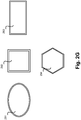
- display configuration 200 may be implemented to provide displays having various shapes, other than circular, and may increase the display active area of the displays being used.
- display configuration 200 may be implemented on an elliptical display 291, a square display 292, a rectangular display 293, and a hexagonal display 294. Since this description is not intended to provide an exhaustive list of possible shapes of a display, shapes other than those specifically described and illustrated may be implemented.
- display configuration 200 may be implemented for various types of user devices.
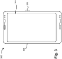
- Fig. 3 illustrates an exemplary user device 300 in which an embodiment of the virtual borderless display may be implemented. While illustratively speaking based on Fig. 3 , user device 300 may be representative of, for example, a smartphone, a cellphone, or a personal digital assistant (PDA), user device 300 may be implemented as various other types of user devices.
- PDA personal digital assistant
- user device 300 may take the form of a tablet device, a data organizer, a picture capturing device, a video capturing device, a Web-access device, a computer, a palmtop device, a netbook, a gaming device, a location-aware device, a music playing device, a television, or some other type of consumer device that comprises a display.
- user device 300 may be implemented as a non-consumer device, a non-mobile device, or any other form of an electronic device.
- user device 300 comprises a housing 305, a microphone 310, a speaker 315, a button 320, and a display 325. Display 325 may be implemented based on display configuration 200, as described herein.
- user device 300 may comprise fewer components, additional components, different components, and/or a different arrangement of components than those illustrated in Fig. 3 and described herein.
- Fig. 4 illustrates another example of a user device 400 in which an embodiment of the virtual borderless display may be implemented.
- user device 400 is representative of a wearable device (e.g., a watch-type user device) that comprises a circular display 405.
- Circular display 405 may be implemented based on display configuration 200, as described herein.
- Fig. 5 illustrates exemplary components of user devices 300 and 400 (simply referred to as user device 300).
- user device 300 comprises a processor 505, memory/storage 510, software 515, a communication interface 520, an input 525, and an output 530.
- user device 300 may comprise fewer components, additional components, different components, and/or a different arrangement of components than those illustrated in Fig. 5 and described herein.
- Processor 505 comprises one or multiple processors, microprocessors, data processors, co-processors, and/or some other type of component that interprets and/or executes instructions and/or data.
- Processor 505 may be implemented as hardware (e.g., a microprocessor, etc.) or a combination of hardware and software (e.g., a system-on-chip (SoC), an application-specific integrated circuit (ASIC), etc.).
- SoC system-on-chip
- ASIC application-specific integrated circuit
- Processor 505 performs one or multiple operations based on an operating system and/or various applications or programs (e.g., software 515).
- Memory/storage 510 comprises one or multiple memories and/or one or multiple other types of storage mediums.
- memory/storage 510 may include a random access memory (RAM), a dynamic random access memory (DRAM), a cache, a read only memory (ROM), a programmable read only memory (PROM), and/or some other type of memory.
- RAM random access memory
- DRAM dynamic random access memory
- ROM read only memory
- PROM programmable read only memory
- Memory/storage 510 may include a hard disk (e.g., a magnetic disk, an optical disk, a magneto-optic disk, a solid state disk, etc.).
- Software 515 comprises an application or a program that provides a function and/or a process.
- Software 515 may include firmware.
- software 515 may comprise a telephone application, a multi-media application, an e-mail application, a contacts application, a calendar application, an instant messaging application, a web browsing application, a location-based application (e.g., a Global Positioning System (GPS)-based application, etc.), a camera application, etc.
- Software 515 comprises an operating system (OS).
- OS operating system
- the operating system may correspond to iOS, Android, Windows Phone, Symbian, or another type of operating system (e.g., proprietary, BlackBerry OS, Windows, Linux, etc.).
- Communication interface 520 permits user device 300 to communicate with other devices, networks, systems, etc.
- Communication interface 520 may include one or multiple wireless interfaces and/or wired interfaces.
- Communication interface 520 may include one or multiple transmitters, receivers, and/or transceivers.
- Communication interface 520 operates according to one or multiple protocols, a communication standard, and/or the like.
- Input 525 permits an input into user device 300.
- input 525 may include a button, a switch, a touch pad, an input port, speech recognition logic, and/or a display (e.g., a touch display, a touchless display).
- Output 230 permits an output from user device 300.
- output 530 may include a speaker, a display, a light, an output port, and/or some other type of output component.
- User device 300 may perform a process and/or a function in response to processor 505 executing software 515 stored by memory/storage 510.
- instructions may be read into memory/storage 510 from another memory/storage 510 or read into memory/storage 510 from another device via communication interface 520.
- the instructions stored by memory/storage 510 causes processor 505 to perform the process or the function.
- user device 300 may perform a process or a function based on the operation of hardware (processor 505, etc.).
Landscapes
- Physics & Mathematics (AREA)
- General Physics & Mathematics (AREA)
- Engineering & Computer Science (AREA)
- Nonlinear Science (AREA)
- Theoretical Computer Science (AREA)
- General Engineering & Computer Science (AREA)
- Mathematical Physics (AREA)
- Chemical & Material Sciences (AREA)
- Crystallography & Structural Chemistry (AREA)
- Optics & Photonics (AREA)
- Human Computer Interaction (AREA)
- Devices For Indicating Variable Information By Combining Individual Elements (AREA)
Claims (12)
- Anzeige (200), umfassend:ein Anzeigepanel (220), das eine obere Fläche und eine untere Fläche aufweist, wobei das Anzeigepanel (220) zwei oder mehr Bondingbereiche (247) an der oberen Fläche umfasst;ein Berührungspanel (210), das in mindestens einem eines Berührungsmodus oder eines berührungslosen Modus betreibbar ist, wobei das Berührungspanel (210) eine obere Fläche und eine untere Fläche aufweist, wobei das Berührungspanel (210) und das Anzeigepanel (220) derart in einem gestapelten Verhältnis sind, dass die obere Fläche des Anzeigepanels (220) an die untere Fläche des Berührungspanels (210) angrenzt und eine Längsachse der Anzeige (200) das Berührungspanel (210) und das Anzeigepanel (220) durchquert;einen Treiber (235), der ausgelegt ist, das Anzeigepanel (220) und das Berührungspanel (210) anzutreiben;eine Schicht (230), die ein Medium bereitstellt, über das Signale sich zu und von dem Treiber (235) ausbreiten können, wobei die Schicht (230) eine obere Fläche und eine untere Fläche aufweist, wobei die Schicht (230) und das Anzeigepanel (220) derart in einem gestapelten Verhältnis sind, dass die obere Fläche der Schicht (230) an die untere Fläche des Anzeigepanels (220) angrenzt und die Längsachse der Anzeige (200) das Anzeigepanel (220) und die Schicht (230) durchquert, und wobei der Treiber (235) an der Schicht (230) angebracht ist; undzwei oder mehr flexible Anzeigepanelverbinder (245), die jeweils ein erstes Ende und ein zweites Ende aufweisen, wobei die zwei oder mehr flexiblen Anzeigepanelverbinder (245) Kommunikationspfade zwischen dem Anzeigepanel (220) und dem Treiber (235) bereitstellen, und sich das erste Ende jedes der zwei oder mehr flexiblen Anzeigepanelverbinder (245) mit dem Anzeigepanel (220) an einem entsprechenden der zwei oder mehr Bondingbereiche (247) verbindet, und sich das zweite Ende jedes der zwei oder mehr flexiblen Anzeigepanelverbinder (245) mit der unteren Fläche der Schicht verbindet, wodurch es sich über die Schicht (230) mit dem Treiber (235) verbindet; undeinen flexiblen Berührungspanelverbinder (240), wobei der flexible Berührungspanelverbinder (240) ein erstes Ende, das mit der unteren Fläche des Berührungspanels (210) verbunden ist, und ein zweites Ende, das mit der unteren Fläche der Schicht (230) verbunden ist, aufweist, wodurch das Berührungspanel (210) über die Schicht mit dem Treiber (235) verbunden wird, und wobei der flexible Berührungspanelverbinder (240) einen Abschnitt aufweist, der radial nach außen von mindestens einem der zwei oder mehr flexiblen Anzeigepanelverbinder (245) beabstandet ist.
- Anzeige nach Anspruch 1, ferner umfassend:
eine Hintergrundbeleuchtung (225), wobei die Hintergrundbeleuchtung (225) zwischen dem Anzeigepanel (220) und der Schicht (230) angeordnet ist, und wobei jeder der zwei oder mehr flexiblen Anzeigepanelverbinder (245) eines einer flexiblen gedruckten Schaltung (245), eines Chip auf Flex oder eines Chip auf Folie umfasst. - Anzeige nach einem der Ansprüche 1-2, wobei die Schicht (230) zwischen dem zweiten Ende jedes der zwei oder mehr flexiblen Anzeigepanelverbinder (245) und dem Anzeigepanel (220) angeordnet ist.
- Anzeige nach einem der Ansprüche 1-3, ferner umfassend:
einen flexiblen Hauptverarbeitungssystemverbinder (250), wobei der flexible Hauptverarbeitungssystemverbinder (250) die Schicht (230) mit einem Hauptverarbeitungssystem einer Benutzervorrichtung verbindet, welche die Anzeige (200) umfasst. - Anzeige nach einem der Ansprüche 1-4, wobei das Anzeigepanel (220) eine einer Flüssigkristallanzeige, einer organischen Leuchtdiodenanzeige oder einer elektrophoretischen Anzeige ist.
- Anzeige nach einem der Ansprüche 1-5, wobei die Schicht (230) eines eines Chip auf Flex, einer gedruckten Schaltungsplatine, eines Chip auf Glas, eines Glaspanels oder einer flexiblen gedruckten Schaltung ist.
- Benutzervorrichtung (300, 400), umfassend:einen Speicher (510), wobei der Speicher Software (515) speichert; undeinen Prozessor (505), wobei der Prozessor (505) ausgelegt ist, die Software (515) auszuführen; undeine Anzeige nach einem der Ansprüche 1-6.
- Benutzervorrichtung (300, 400) nach Anspruch 7, wobei die Anzeige (200, 325, 405) ferner eine Hintergrundbeleuchtung (225) umfasst, und wobei die Hintergrundbeleuchtung (225) zwischen dem Anzeigepanel (220) und der Schicht (230) angeordnet ist.
- Benutzervorrichtung (300, 400) nach einem der Ansprüche 7-8, wobei die Schicht (230) zwischen dem zweiten Ende jedes der zwei oder mehr flexiblen Anzeigepanelverbinder (245) und dem Anzeigepanel (220) angeordnet ist.
- Benutzervorrichtung (300, 400) nach einem der Ansprüche 7-9, ferner umfassend:
einen flexiblen Verbinder (245), wobei der flexible Verbinder die Schicht (230) mit einem Hauptverarbeitungssystem der Benutzervorrichtung (300) verbindet. - Benutzervorrichtung (300, 400) nach Anspruch 10, wobei das Anzeigepanel (220) umfasst:eine Dünnfilmtransistorschicht; undeine Farbfilterschicht, und wobei die zwei oder mehr Bondingbereiche (247) auf der Dünnfilmtransistorschicht angeordnet sind, und wobei die Dünnfilmtransistorschicht und die Farbfilterschicht eine kreisförmige Auslegung aufweisen.
- Benutzervorrichtung (300, 400) nach einem der Ansprüche 7-11, wobei das Anzeigepanel (220) eine einer Flüssigkristallanzeige, einer organischen Leuchtdiodenanzeige oder einer elektrophoretischen Anzeige ist.
Applications Claiming Priority (2)
| Application Number | Priority Date | Filing Date | Title |
|---|---|---|---|
| US14/673,955 US10067583B2 (en) | 2015-03-31 | 2015-03-31 | Virtual borderless display |
| PCT/US2015/052527 WO2016160054A1 (en) | 2015-03-31 | 2015-09-26 | Virtual borderless display |
Publications (2)
| Publication Number | Publication Date |
|---|---|
| EP3278326A1 EP3278326A1 (de) | 2018-02-07 |
| EP3278326B1 true EP3278326B1 (de) | 2021-07-21 |
Family
ID=54325693
Family Applications (1)
| Application Number | Title | Priority Date | Filing Date |
|---|---|---|---|
| EP15781216.5A Active EP3278326B1 (de) | 2015-03-31 | 2015-09-26 | Virtuelle grenzenlose anzeige |
Country Status (3)
| Country | Link |
|---|---|
| US (1) | US10067583B2 (de) |
| EP (1) | EP3278326B1 (de) |
| WO (1) | WO2016160054A1 (de) |
Families Citing this family (13)
| Publication number | Priority date | Publication date | Assignee | Title |
|---|---|---|---|---|
| US10261370B2 (en) | 2011-10-05 | 2019-04-16 | Apple Inc. | Displays with minimized border regions having an apertured TFT layer for signal conductors |
| KR102315671B1 (ko) * | 2015-01-19 | 2021-10-21 | 삼성디스플레이 주식회사 | 표시 장치 |
| US10691248B2 (en) * | 2015-09-08 | 2020-06-23 | Lg Display Co., Ltd. | Driving circuit, touch display device, and method for driving the touch display device |
| EP3141988B1 (de) | 2015-09-08 | 2022-07-20 | LG Display Co., Ltd. | In-zellen-berührungsanzeigevorrichtung |
| KR102483379B1 (ko) * | 2015-09-21 | 2023-01-02 | 삼성디스플레이 주식회사 | 표시장치 |
| US10162311B2 (en) * | 2015-12-15 | 2018-12-25 | Qualcomm Incorporated | Display panel with minimum borders |
| US9791833B1 (en) * | 2016-04-13 | 2017-10-17 | Google Inc. | Physical watch hands for a computerized watch |
| CN107232700A (zh) * | 2017-06-12 | 2017-10-10 | 捷开通讯(深圳)有限公司 | 一种智能穿戴设备 |
| KR102420019B1 (ko) * | 2017-08-07 | 2022-07-12 | 삼성전자주식회사 | 웨어러블 디바이스 및 전자 기기 |
| KR102433103B1 (ko) * | 2017-10-02 | 2022-08-17 | 삼성디스플레이 주식회사 | 표시 장치 |
| US11099439B2 (en) | 2018-09-11 | 2021-08-24 | Apple Inc. | Display device assembly having a spacer layer surrounding the integrated circuit |
| US20250383632A1 (en) * | 2022-09-16 | 2025-12-18 | Honor Device Co., Ltd. | Electronic device |
| WO2025150854A1 (ko) * | 2024-01-09 | 2025-07-17 | 삼성전자 주식회사 | 디스플레이 패널을 포함하는 웨어러블 전자 장치 및 그 제어 방법 |
Citations (2)
| Publication number | Priority date | Publication date | Assignee | Title |
|---|---|---|---|---|
| US20100134743A1 (en) * | 2008-12-02 | 2010-06-03 | Samsung Electonics Co, Ltd. | Display substrate, display panel having the display substrate, and display device having the display panel |
| US20130181951A1 (en) * | 2011-05-23 | 2013-07-18 | Sony Ericsson Mobile Communications Ab | Finger-on display detection |
Family Cites Families (21)
| Publication number | Priority date | Publication date | Assignee | Title |
|---|---|---|---|---|
| GB9311379D0 (en) | 1993-06-02 | 1993-07-21 | Philips Electronics Uk Ltd | Programming/reprogramming a radio apparatus |
| JPH07152019A (ja) * | 1993-11-30 | 1995-06-16 | Matsushita Electric Ind Co Ltd | 液晶表示装置 |
| KR100534376B1 (ko) | 1999-06-21 | 2005-12-08 | 엘지.필립스 엘시디 주식회사 | 디지타이저를 가진 액정표시소자 |
| TWI310860B (en) | 2002-11-13 | 2009-06-11 | Toppoly Optoelectronics Corp | Assembly structure for flat panel display |
| TWI230827B (en) | 2004-02-12 | 2005-04-11 | Au Optronics Corp | Liquid crystal display module |
| JP4251203B2 (ja) * | 2006-08-29 | 2009-04-08 | セイコーエプソン株式会社 | 貼合せマザー基板のスクライブ方法および貼合せマザー基板の分割方法 |
| KR101342652B1 (ko) | 2006-11-15 | 2013-12-16 | 삼성디스플레이 주식회사 | 액정 표시 장치 |
| KR101323454B1 (ko) | 2008-10-08 | 2013-10-29 | 엘지디스플레이 주식회사 | 백라이트 유닛 및 이를 구비한 액정표시장치 |
| KR101529921B1 (ko) | 2008-11-04 | 2015-06-18 | 엘지전자 주식회사 | 와치형 단말기 |
| KR101626621B1 (ko) | 2009-12-30 | 2016-06-01 | 엘지전자 주식회사 | 원형 디스플레이부를 구비한 이동 통신 단말기의 데이터 제어 방법 및 이를 적용한 이동 통신 단말기 |
| KR101659023B1 (ko) | 2010-03-15 | 2016-09-23 | 엘지전자 주식회사 | 와치형 이동 단말기 |
| JP2012093498A (ja) | 2010-10-26 | 2012-05-17 | Hitachi Displays Ltd | 画像表示装置 |
| KR101813033B1 (ko) * | 2011-05-13 | 2017-12-28 | 엘지전자 주식회사 | 이동 단말기 |
| KR101861628B1 (ko) * | 2011-09-16 | 2018-05-29 | 삼성디스플레이 주식회사 | 액정 표시 장치 |
| US10261370B2 (en) | 2011-10-05 | 2019-04-16 | Apple Inc. | Displays with minimized border regions having an apertured TFT layer for signal conductors |
| US9894781B2 (en) | 2012-06-06 | 2018-02-13 | Apple Inc. | Notched display layers |
| US9454025B2 (en) | 2012-08-31 | 2016-09-27 | Apple Inc. | Displays with reduced driver circuit ledges |
| WO2014054418A1 (ja) | 2012-10-03 | 2014-04-10 | シャープ株式会社 | 表示装置 |
| KR101973780B1 (ko) | 2012-10-08 | 2019-04-30 | 삼성디스플레이 주식회사 | 표시 장치 |
| KR102038883B1 (ko) | 2013-05-22 | 2019-10-31 | 엘지디스플레이 주식회사 | 표시장치 및 그 구동방법 |
| EP2813907B1 (de) | 2013-06-11 | 2018-08-01 | LG Electronics, Inc. | Uhrenartiges mobiles Terminal |
-
2015
- 2015-03-31 US US14/673,955 patent/US10067583B2/en active Active
- 2015-09-26 WO PCT/US2015/052527 patent/WO2016160054A1/en not_active Ceased
- 2015-09-26 EP EP15781216.5A patent/EP3278326B1/de active Active
Patent Citations (2)
| Publication number | Priority date | Publication date | Assignee | Title |
|---|---|---|---|---|
| US20100134743A1 (en) * | 2008-12-02 | 2010-06-03 | Samsung Electonics Co, Ltd. | Display substrate, display panel having the display substrate, and display device having the display panel |
| US20130181951A1 (en) * | 2011-05-23 | 2013-07-18 | Sony Ericsson Mobile Communications Ab | Finger-on display detection |
Also Published As
| Publication number | Publication date |
|---|---|
| US20160291745A1 (en) | 2016-10-06 |
| US10067583B2 (en) | 2018-09-04 |
| EP3278326A1 (de) | 2018-02-07 |
| WO2016160054A1 (en) | 2016-10-06 |
Similar Documents
| Publication | Publication Date | Title |
|---|---|---|
| EP3278326B1 (de) | Virtuelle grenzenlose anzeige | |
| US9547208B2 (en) | Divided backlight configuration of a display | |
| EP3690600B1 (de) | Faltbare anzeige mit steifer stütze | |
| CN113454564B (zh) | 可折叠电子装置 | |
| US8716932B2 (en) | Displays with minimized borders | |
| US10777769B2 (en) | Protective film for protecting display panel, and display module and display device having the same | |
| US9971436B2 (en) | Touch user interface at a display edge | |
| KR102338473B1 (ko) | 윈도우 커버, 이를 가지는 디스플레이장치 및 그 제조방법 | |
| US10957867B2 (en) | Display device | |
| CN202929522U (zh) | 信息处理设备 | |
| US10254451B2 (en) | Display device | |
| JP2016504805A (ja) | 複数のディスプレイを有するモバイルデバイス | |
| CN106504645A (zh) | 柔性显示面板及柔性显示设备 | |
| CN205068333U (zh) | 电子显示模块及电子装置 | |
| US20200333844A1 (en) | Flexible display device | |
| US9983338B2 (en) | Optical member and display device including the same | |
| CN111630445A (zh) | 包括弯曲区域中的多个布线层的显示器 | |
| US20140285733A1 (en) | Touch display apparatus and method for manufacturing the same | |
| US20160378231A1 (en) | Display device | |
| US20140062920A1 (en) | Touch panel | |
| CN116830068A (zh) | 用于可穿戴设备的oled显示器的触敏边框区域 | |
| US20160313490A1 (en) | Integrated light source in recess of housing | |
| CN112700728A (zh) | 显示模组及电子设备 | |
| JP2026053289A (ja) | ディスプレイ支持体を有する電子デバイス | |
| US20140118288A1 (en) | Mechanical structure for system using flush surface display design |
Legal Events
| Date | Code | Title | Description |
|---|---|---|---|
| STAA | Information on the status of an ep patent application or granted ep patent |
Free format text: STATUS: THE INTERNATIONAL PUBLICATION HAS BEEN MADE |
|
| PUAI | Public reference made under article 153(3) epc to a published international application that has entered the european phase |
Free format text: ORIGINAL CODE: 0009012 |
|
| STAA | Information on the status of an ep patent application or granted ep patent |
Free format text: STATUS: REQUEST FOR EXAMINATION WAS MADE |
|
| 17P | Request for examination filed |
Effective date: 20171030 |
|
| AK | Designated contracting states |
Kind code of ref document: A1 Designated state(s): AL AT BE BG CH CY CZ DE DK EE ES FI FR GB GR HR HU IE IS IT LI LT LU LV MC MK MT NL NO PL PT RO RS SE SI SK SM TR |
|
| AX | Request for extension of the european patent |
Extension state: BA ME |
|
| DAV | Request for validation of the european patent (deleted) | ||
| DAX | Request for extension of the european patent (deleted) | ||
| STAA | Information on the status of an ep patent application or granted ep patent |
Free format text: STATUS: EXAMINATION IS IN PROGRESS |
|
| 17Q | First examination report despatched |
Effective date: 20200206 |
|
| GRAP | Despatch of communication of intention to grant a patent |
Free format text: ORIGINAL CODE: EPIDOSNIGR1 |
|
| STAA | Information on the status of an ep patent application or granted ep patent |
Free format text: STATUS: GRANT OF PATENT IS INTENDED |
|
| INTG | Intention to grant announced |
Effective date: 20210212 |
|
| RIN1 | Information on inventor provided before grant (corrected) |
Inventor name: GRIP, MARTIN |
|
| GRAS | Grant fee paid |
Free format text: ORIGINAL CODE: EPIDOSNIGR3 |
|
| GRAA | (expected) grant |
Free format text: ORIGINAL CODE: 0009210 |
|
| STAA | Information on the status of an ep patent application or granted ep patent |
Free format text: STATUS: THE PATENT HAS BEEN GRANTED |
|
| RAP3 | Party data changed (applicant data changed or rights of an application transferred) |
Owner name: SONY GROUP CORPORATION |
|
| AK | Designated contracting states |
Kind code of ref document: B1 Designated state(s): AL AT BE BG CH CY CZ DE DK EE ES FI FR GB GR HR HU IE IS IT LI LT LU LV MC MK MT NL NO PL PT RO RS SE SI SK SM TR |
|
| REG | Reference to a national code |
Ref country code: GB Ref legal event code: FG4D |
|
| REG | Reference to a national code |
Ref country code: CH Ref legal event code: EP |
|
| REG | Reference to a national code |
Ref country code: DE Ref legal event code: R096 Ref document number: 602015071501 Country of ref document: DE |
|
| REG | Reference to a national code |
Ref country code: AT Ref legal event code: REF Ref document number: 1413314 Country of ref document: AT Kind code of ref document: T Effective date: 20210815 |
|
| REG | Reference to a national code |
Ref country code: IE Ref legal event code: FG4D |
|
| REG | Reference to a national code |
Ref country code: LT Ref legal event code: MG9D |
|
| REG | Reference to a national code |
Ref country code: NL Ref legal event code: MP Effective date: 20210721 |
|
| REG | Reference to a national code |
Ref country code: AT Ref legal event code: MK05 Ref document number: 1413314 Country of ref document: AT Kind code of ref document: T Effective date: 20210721 |
|
| PG25 | Lapsed in a contracting state [announced via postgrant information from national office to epo] |
Ref country code: HR Free format text: LAPSE BECAUSE OF FAILURE TO SUBMIT A TRANSLATION OF THE DESCRIPTION OR TO PAY THE FEE WITHIN THE PRESCRIBED TIME-LIMIT Effective date: 20210721 Ref country code: SE Free format text: LAPSE BECAUSE OF FAILURE TO SUBMIT A TRANSLATION OF THE DESCRIPTION OR TO PAY THE FEE WITHIN THE PRESCRIBED TIME-LIMIT Effective date: 20210721 Ref country code: RS Free format text: LAPSE BECAUSE OF FAILURE TO SUBMIT A TRANSLATION OF THE DESCRIPTION OR TO PAY THE FEE WITHIN THE PRESCRIBED TIME-LIMIT Effective date: 20210721 Ref country code: NO Free format text: LAPSE BECAUSE OF FAILURE TO SUBMIT A TRANSLATION OF THE DESCRIPTION OR TO PAY THE FEE WITHIN THE PRESCRIBED TIME-LIMIT Effective date: 20211021 Ref country code: NL Free format text: LAPSE BECAUSE OF FAILURE TO SUBMIT A TRANSLATION OF THE DESCRIPTION OR TO PAY THE FEE WITHIN THE PRESCRIBED TIME-LIMIT Effective date: 20210721 Ref country code: PT Free format text: LAPSE BECAUSE OF FAILURE TO SUBMIT A TRANSLATION OF THE DESCRIPTION OR TO PAY THE FEE WITHIN THE PRESCRIBED TIME-LIMIT Effective date: 20211122 Ref country code: FI Free format text: LAPSE BECAUSE OF FAILURE TO SUBMIT A TRANSLATION OF THE DESCRIPTION OR TO PAY THE FEE WITHIN THE PRESCRIBED TIME-LIMIT Effective date: 20210721 Ref country code: ES Free format text: LAPSE BECAUSE OF FAILURE TO SUBMIT A TRANSLATION OF THE DESCRIPTION OR TO PAY THE FEE WITHIN THE PRESCRIBED TIME-LIMIT Effective date: 20210721 Ref country code: LT Free format text: LAPSE BECAUSE OF FAILURE TO SUBMIT A TRANSLATION OF THE DESCRIPTION OR TO PAY THE FEE WITHIN THE PRESCRIBED TIME-LIMIT Effective date: 20210721 Ref country code: BG Free format text: LAPSE BECAUSE OF FAILURE TO SUBMIT A TRANSLATION OF THE DESCRIPTION OR TO PAY THE FEE WITHIN THE PRESCRIBED TIME-LIMIT Effective date: 20211021 Ref country code: AT Free format text: LAPSE BECAUSE OF FAILURE TO SUBMIT A TRANSLATION OF THE DESCRIPTION OR TO PAY THE FEE WITHIN THE PRESCRIBED TIME-LIMIT Effective date: 20210721 |
|
| PG25 | Lapsed in a contracting state [announced via postgrant information from national office to epo] |
Ref country code: PL Free format text: LAPSE BECAUSE OF FAILURE TO SUBMIT A TRANSLATION OF THE DESCRIPTION OR TO PAY THE FEE WITHIN THE PRESCRIBED TIME-LIMIT Effective date: 20210721 Ref country code: LV Free format text: LAPSE BECAUSE OF FAILURE TO SUBMIT A TRANSLATION OF THE DESCRIPTION OR TO PAY THE FEE WITHIN THE PRESCRIBED TIME-LIMIT Effective date: 20210721 Ref country code: GR Free format text: LAPSE BECAUSE OF FAILURE TO SUBMIT A TRANSLATION OF THE DESCRIPTION OR TO PAY THE FEE WITHIN THE PRESCRIBED TIME-LIMIT Effective date: 20211022 |
|
| REG | Reference to a national code |
Ref country code: DE Ref legal event code: R097 Ref document number: 602015071501 Country of ref document: DE |
|
| PG25 | Lapsed in a contracting state [announced via postgrant information from national office to epo] |
Ref country code: DK Free format text: LAPSE BECAUSE OF FAILURE TO SUBMIT A TRANSLATION OF THE DESCRIPTION OR TO PAY THE FEE WITHIN THE PRESCRIBED TIME-LIMIT Effective date: 20210721 |
|
| REG | Reference to a national code |
Ref country code: CH Ref legal event code: PL |
|
| REG | Reference to a national code |
Ref country code: BE Ref legal event code: MM Effective date: 20210930 |
|
| PLBE | No opposition filed within time limit |
Free format text: ORIGINAL CODE: 0009261 |
|
| STAA | Information on the status of an ep patent application or granted ep patent |
Free format text: STATUS: NO OPPOSITION FILED WITHIN TIME LIMIT |
|
| PG25 | Lapsed in a contracting state [announced via postgrant information from national office to epo] |
Ref country code: SM Free format text: LAPSE BECAUSE OF FAILURE TO SUBMIT A TRANSLATION OF THE DESCRIPTION OR TO PAY THE FEE WITHIN THE PRESCRIBED TIME-LIMIT Effective date: 20210721 Ref country code: SK Free format text: LAPSE BECAUSE OF FAILURE TO SUBMIT A TRANSLATION OF THE DESCRIPTION OR TO PAY THE FEE WITHIN THE PRESCRIBED TIME-LIMIT Effective date: 20210721 Ref country code: RO Free format text: LAPSE BECAUSE OF FAILURE TO SUBMIT A TRANSLATION OF THE DESCRIPTION OR TO PAY THE FEE WITHIN THE PRESCRIBED TIME-LIMIT Effective date: 20210721 Ref country code: MC Free format text: LAPSE BECAUSE OF FAILURE TO SUBMIT A TRANSLATION OF THE DESCRIPTION OR TO PAY THE FEE WITHIN THE PRESCRIBED TIME-LIMIT Effective date: 20210721 Ref country code: EE Free format text: LAPSE BECAUSE OF FAILURE TO SUBMIT A TRANSLATION OF THE DESCRIPTION OR TO PAY THE FEE WITHIN THE PRESCRIBED TIME-LIMIT Effective date: 20210721 Ref country code: CZ Free format text: LAPSE BECAUSE OF FAILURE TO SUBMIT A TRANSLATION OF THE DESCRIPTION OR TO PAY THE FEE WITHIN THE PRESCRIBED TIME-LIMIT Effective date: 20210721 Ref country code: AL Free format text: LAPSE BECAUSE OF FAILURE TO SUBMIT A TRANSLATION OF THE DESCRIPTION OR TO PAY THE FEE WITHIN THE PRESCRIBED TIME-LIMIT Effective date: 20210721 |
|
| 26N | No opposition filed |
Effective date: 20220422 |
|
| PG25 | Lapsed in a contracting state [announced via postgrant information from national office to epo] |
Ref country code: LU Free format text: LAPSE BECAUSE OF NON-PAYMENT OF DUE FEES Effective date: 20210926 Ref country code: IT Free format text: LAPSE BECAUSE OF FAILURE TO SUBMIT A TRANSLATION OF THE DESCRIPTION OR TO PAY THE FEE WITHIN THE PRESCRIBED TIME-LIMIT Effective date: 20210721 Ref country code: IE Free format text: LAPSE BECAUSE OF NON-PAYMENT OF DUE FEES Effective date: 20210926 Ref country code: FR Free format text: LAPSE BECAUSE OF NON-PAYMENT OF DUE FEES Effective date: 20210930 Ref country code: BE Free format text: LAPSE BECAUSE OF NON-PAYMENT OF DUE FEES Effective date: 20210930 |
|
| PG25 | Lapsed in a contracting state [announced via postgrant information from national office to epo] |
Ref country code: LI Free format text: LAPSE BECAUSE OF NON-PAYMENT OF DUE FEES Effective date: 20210930 Ref country code: CH Free format text: LAPSE BECAUSE OF NON-PAYMENT OF DUE FEES Effective date: 20210930 |
|
| PG25 | Lapsed in a contracting state [announced via postgrant information from national office to epo] |
Ref country code: HU Free format text: LAPSE BECAUSE OF FAILURE TO SUBMIT A TRANSLATION OF THE DESCRIPTION OR TO PAY THE FEE WITHIN THE PRESCRIBED TIME-LIMIT; INVALID AB INITIO Effective date: 20150926 |
|
| PG25 | Lapsed in a contracting state [announced via postgrant information from national office to epo] |
Ref country code: CY Free format text: LAPSE BECAUSE OF FAILURE TO SUBMIT A TRANSLATION OF THE DESCRIPTION OR TO PAY THE FEE WITHIN THE PRESCRIBED TIME-LIMIT Effective date: 20210721 |
|
| P01 | Opt-out of the competence of the unified patent court (upc) registered |
Effective date: 20230527 |
|
| PGFP | Annual fee paid to national office [announced via postgrant information from national office to epo] |
Ref country code: GB Payment date: 20230823 Year of fee payment: 9 |
|
| PGFP | Annual fee paid to national office [announced via postgrant information from national office to epo] |
Ref country code: DE Payment date: 20230822 Year of fee payment: 9 |
|
| PG25 | Lapsed in a contracting state [announced via postgrant information from national office to epo] |
Ref country code: MK Free format text: LAPSE BECAUSE OF FAILURE TO SUBMIT A TRANSLATION OF THE DESCRIPTION OR TO PAY THE FEE WITHIN THE PRESCRIBED TIME-LIMIT Effective date: 20210721 |
|
| PG25 | Lapsed in a contracting state [announced via postgrant information from national office to epo] |
Ref country code: MT Free format text: LAPSE BECAUSE OF FAILURE TO SUBMIT A TRANSLATION OF THE DESCRIPTION OR TO PAY THE FEE WITHIN THE PRESCRIBED TIME-LIMIT Effective date: 20210721 |
|
| REG | Reference to a national code |
Ref country code: DE Ref legal event code: R119 Ref document number: 602015071501 Country of ref document: DE |
|
| GBPC | Gb: european patent ceased through non-payment of renewal fee |
Effective date: 20240926 |
|
| PG25 | Lapsed in a contracting state [announced via postgrant information from national office to epo] |
Ref country code: DE Free format text: LAPSE BECAUSE OF NON-PAYMENT OF DUE FEES Effective date: 20250401 |
|
| PG25 | Lapsed in a contracting state [announced via postgrant information from national office to epo] |
Ref country code: GB Free format text: LAPSE BECAUSE OF NON-PAYMENT OF DUE FEES Effective date: 20240926 |
|
| PG25 | Lapsed in a contracting state [announced via postgrant information from national office to epo] |
Ref country code: TR Free format text: LAPSE BECAUSE OF FAILURE TO SUBMIT A TRANSLATION OF THE DESCRIPTION OR TO PAY THE FEE WITHIN THE PRESCRIBED TIME-LIMIT Effective date: 20210721 |