EP3268758B1 - Hochauflösender sigma-delta-modulator zur messung der verschiebung einer kapazitätssensorklemme - Google Patents
Hochauflösender sigma-delta-modulator zur messung der verschiebung einer kapazitätssensorklemme Download PDFInfo
- Publication number
- EP3268758B1 EP3268758B1 EP16765513.3A EP16765513A EP3268758B1 EP 3268758 B1 EP3268758 B1 EP 3268758B1 EP 16765513 A EP16765513 A EP 16765513A EP 3268758 B1 EP3268758 B1 EP 3268758B1
- Authority
- EP
- European Patent Office
- Prior art keywords
- sensor
- excitation
- capacitance
- sensor circuit
- excitation voltage
- Prior art date
- Legal status (The legal status is an assumption and is not a legal conclusion. Google has not performed a legal analysis and makes no representation as to the accuracy of the status listed.)
- Active
Links
Images




Classifications
-
- G—PHYSICS
- G01—MEASURING; TESTING
- G01D—MEASURING NOT SPECIALLY ADAPTED FOR A SPECIFIC VARIABLE; ARRANGEMENTS FOR MEASURING TWO OR MORE VARIABLES NOT COVERED IN A SINGLE OTHER SUBCLASS; TARIFF METERING APPARATUS; MEASURING OR TESTING NOT OTHERWISE PROVIDED FOR
- G01D5/00—Mechanical means for transferring the output of a sensing member; Means for converting the output of a sensing member to another variable where the form or nature of the sensing member does not constrain the means for converting; Transducers not specially adapted for a specific variable
- G01D5/12—Mechanical means for transferring the output of a sensing member; Means for converting the output of a sensing member to another variable where the form or nature of the sensing member does not constrain the means for converting; Transducers not specially adapted for a specific variable using electric or magnetic means
- G01D5/14—Mechanical means for transferring the output of a sensing member; Means for converting the output of a sensing member to another variable where the form or nature of the sensing member does not constrain the means for converting; Transducers not specially adapted for a specific variable using electric or magnetic means influencing the magnitude of a current or voltage
- G01D5/24—Mechanical means for transferring the output of a sensing member; Means for converting the output of a sensing member to another variable where the form or nature of the sensing member does not constrain the means for converting; Transducers not specially adapted for a specific variable using electric or magnetic means influencing the magnitude of a current or voltage by varying capacitance
-
- G—PHYSICS
- G01—MEASURING; TESTING
- G01L—MEASURING FORCE, STRESS, TORQUE, WORK, MECHANICAL POWER, MECHANICAL EFFICIENCY, OR FLUID PRESSURE
- G01L9/00—Measuring steady of quasi-steady pressure of fluid or fluent solid material by electric or magnetic pressure-sensitive elements; Transmitting or indicating the displacement of mechanical pressure-sensitive elements, used to measure the steady or quasi-steady pressure of a fluid or fluent solid material, by electric or magnetic means
- G01L9/0041—Transmitting or indicating the displacement of flexible diaphragms
- G01L9/0072—Transmitting or indicating the displacement of flexible diaphragms using variations in capacitance
-
- G—PHYSICS
- G01—MEASURING; TESTING
- G01L—MEASURING FORCE, STRESS, TORQUE, WORK, MECHANICAL POWER, MECHANICAL EFFICIENCY, OR FLUID PRESSURE
- G01L9/00—Measuring steady of quasi-steady pressure of fluid or fluent solid material by electric or magnetic pressure-sensitive elements; Transmitting or indicating the displacement of mechanical pressure-sensitive elements, used to measure the steady or quasi-steady pressure of a fluid or fluent solid material, by electric or magnetic means
- G01L9/0041—Transmitting or indicating the displacement of flexible diaphragms
- G01L9/0072—Transmitting or indicating the displacement of flexible diaphragms using variations in capacitance
- G01L9/0075—Transmitting or indicating the displacement of flexible diaphragms using variations in capacitance using a ceramic diaphragm, e.g. alumina, fused quartz, glass
-
- G—PHYSICS
- G01—MEASURING; TESTING
- G01L—MEASURING FORCE, STRESS, TORQUE, WORK, MECHANICAL POWER, MECHANICAL EFFICIENCY, OR FLUID PRESSURE
- G01L9/00—Measuring steady of quasi-steady pressure of fluid or fluent solid material by electric or magnetic pressure-sensitive elements; Transmitting or indicating the displacement of mechanical pressure-sensitive elements, used to measure the steady or quasi-steady pressure of a fluid or fluent solid material, by electric or magnetic means
- G01L9/12—Measuring steady of quasi-steady pressure of fluid or fluent solid material by electric or magnetic pressure-sensitive elements; Transmitting or indicating the displacement of mechanical pressure-sensitive elements, used to measure the steady or quasi-steady pressure of a fluid or fluent solid material, by electric or magnetic means by making use of variations in capacitance, i.e. electric circuits therefor
-
- H—ELECTRICITY
- H03—ELECTRONIC CIRCUITRY
- H03M—CODING; DECODING; CODE CONVERSION IN GENERAL
- H03M3/00—Conversion of analogue values to or from differential modulation
- H03M3/30—Delta-sigma modulation
- H03M3/39—Structural details of delta-sigma modulators, e.g. incremental delta-sigma modulators
-
- H—ELECTRICITY
- H03—ELECTRONIC CIRCUITRY
- H03M—CODING; DECODING; CODE CONVERSION IN GENERAL
- H03M3/00—Conversion of analogue values to or from differential modulation
- H03M3/30—Delta-sigma modulation
- H03M3/458—Analogue/digital converters using delta-sigma modulation as an intermediate step
- H03M3/494—Sampling or signal conditioning arrangements specially adapted for delta-sigma type analogue/digital conversion systems
-
- H—ELECTRICITY
- H03—ELECTRONIC CIRCUITRY
- H03M—CODING; DECODING; CODE CONVERSION IN GENERAL
- H03M3/00—Conversion of analogue values to or from differential modulation
- H03M3/30—Delta-sigma modulation
- H03M3/322—Continuously compensating for, or preventing, undesired influence of physical parameters
- H03M3/352—Continuously compensating for, or preventing, undesired influence of physical parameters of deviations from the desired transfer characteristic
- H03M3/354—Continuously compensating for, or preventing, undesired influence of physical parameters of deviations from the desired transfer characteristic at one point, i.e. by adjusting a single reference value, e.g. bias or gain error
- H03M3/356—Offset or drift compensation
-
- H—ELECTRICITY
- H03—ELECTRONIC CIRCUITRY
- H03M—CODING; DECODING; CODE CONVERSION IN GENERAL
- H03M3/00—Conversion of analogue values to or from differential modulation
- H03M3/30—Delta-sigma modulation
- H03M3/322—Continuously compensating for, or preventing, undesired influence of physical parameters
- H03M3/368—Continuously compensating for, or preventing, undesired influence of physical parameters of noise other than the quantisation noise already being shaped inherently by delta-sigma modulators
- H03M3/376—Prevention or reduction of switching transients, e.g. glitches
Definitions
- the present invention relates capacitance type sensors and to the conversion of the variable capacitance of the sensor to a digital value.
- Capacitance sensors have found a wide range of applications. Capacitance sensors are used for sensing pressure, acceleration, flow, humidity, proximity, angle, rotation, as well as human interface sensing applications. For example, capacitance sensors are used for differential pressure measurement as well as absolute pressure measurement.
- variable capacitance produced by a capacitance sensor must be converted to an electrical signal that can be processed to produce a measurement output.
- electrical signal it is desirable to produce the electrical signal as a digital value that represents the variable capacitance, so that further signal processing can be done with digital circuitry rather than analog circuitry.
- Capacitance-to-digital (C/D) converters using sigma delta modulators have been used in conjunction with capacitance sensors.
- One example is the use of sigma delta modulators for C/D conversion is in conjunction with capacitance pressure sensors.
- the present invention is defined by the appended independent apparatus claim 1.
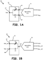
- FIGS. 1A and 1B show two alternative capacitance-to-digital (C/D) excitation schemes for a single plate terminal displacement capacitance sensor.
- a terminal displacement capacitance sensor is one in which the spacing between the plates forming the sensor change in relation to the sensed parameter. Thus the capacitance of the sensor changes in relation to the sensed parameter.
- FIG. 1A shows sensor circuit 10, which includes capacitance sensor 12 and capacitance-to-digital (C/D) sigma delta modulator 14.
- Sensor 12 includes sensor capacitor CS and reference capacitor CR, which share a common plate.
- Sensor 12 has three terminals, common plate terminal CP, sensor plate terminal SP, and reference plate terminal RP. Terminals SP and RP are connected to inputs of modulator 14.
- Common plate terminal CP receives a single two-phase excitation signal V exc that excites both sensor capacitor CS and reference capacitor CR.
- Modulator 14 produces a pulse code modulated output signal PCM and excitation signal V exc .
- Sensor circuit 10 produces a digitized signal (output signal PCM) from which a capacitance of sensor capacitor CS can be determined.
- output signal PCM digitized signal
- the digitized signal produced by modulator 14 has been found to be deficient in several characteristics.
- the digitized signal is nonlinear with pressure. This complicates signal compensation and makes resolution performance dependent on applied pressure.
- the digitized signal results in low utilization of analog-to-digital (A/D) converter range. This contributes to poor resolution due to the low sensitivity of the output of modulator 14 with respect to the pressure input to sensor 12. The sensitivity is lowest near the zero pressure input condition to sensor 12.
- the excitation signal has a low signal level. This contributes to poor resolution because the driven sensor signals are relatively low compared to the intrinsic thermal noise within sensor circuit 10.
- circuit 10 is not optimal.
- Sensor circuit 10 will be described in more detail with reference to FIGS. 2 , 3A , 3B , 4A, and 4B .
- FIG. 1B shows sensor circuit 20, which includes single plate terminal displacement capacitance sensor 22 and C/D sigma delta modulator 24.
- Capacitance sensor 22 is similar to capacitance sensor 12.
- Sensor 22 includes sensor capacitor CS and reference capacitor CR, with common plate terminal CP connected to the input of C/D circuit 24.
- Sensor plate terminal SP receives sensor excitation signal V exc_sen
- reference plate terminal RP receives reference excitation signal V exc_ref .
- Modulator 24 produces a pulse code modulated output signal PCM, as well as sensor excitation signal V exc_sen and reference excitation signal V exc_ref .
- Sensor circuit 20 offers higher resolution than sensor circuit 10. It addresses the deficiencies in the digitized signal discussed above with respect to sensor circuit 10.
- FIGS. 5-7B describe sensor circuit 20A, which uses a first order two-phase sigma delta modulator.
- FIGS. 8-11 describe sensor circuit 20B, which uses a second order two-phase sigma delta modulator.
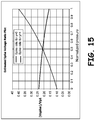
- FIGS. 12-15 describe sensor circuit 20C, which uses a first order two-phase modulator that includes a programmable ratio-metric excitation voltage generator.
- FIGS. 16-17C illustrate sensor circuit 20D, which uses a second order two-phase sigma delta modulator with a programmable ratio-metric excitation voltage generator.
- FIGS. 18-19B show sensor circuit 20E utilizing a second order two-phase sigma delta modulator that includes an adaptive excitation voltage control and a programmable ratio-metric excitation voltage generator.
- Capacitance sensors 12 and 22 are a single plate terminal displacement sensors that can be used, for example, to provide an absolute pressure (AP) measurement.
- Sensors 12, 22 include sensor capacitor CS (with a capacitance C SENSOR ) and reference capacitor CR (with capacitance C REF ).
- Sensor capacitor CS and reference capacitor CR share common plate terminal CP.
- C SA active sensing capacitance
- C P parasitic capacitance
- P ⁇ A is normalized absolute pressure with dynamic range of [0, 1]
- ⁇ is normalized elastic constant.
- FIG. 2 shows a basic configuration of existing sensor circuit 10.
- Sensor circuit 10 includes capacitance sensor 12 and C/D sigma delta modulator 14 as discussed in reference to FIG. 1A .
- Modulator 14 includes integrator 30, quantizer 32, and excitation signal generator 34.
- Integrator 30 is a first stage integrator, and includes operational amplifier (op amp) 36, switches 38, 40, 42, 44, 46, 48, and 50, auto-zero capacitor CZ and feedback capacitor CF1.
- Quantizer 32 includes comparator 52 and latch 54.
- Excitation signal generator 34 includes switches 56 and 58.
- Also shown in FIG. 2 are clock signals ⁇ 1 and ⁇ 2, which produce two-phase operation of modulator 14.
- Modulator 14 makes use of three voltage levels, VP, VMID, and VN.
- VMID is a voltage midway between VDDA and VSSA.
- switches 38 and 44 are closed when output y of latch 54 is “1" or high, and switches 40 and 42 are closed when output y of latch 54 is “1" or high.
- Switches 48 and 50 are closed when ⁇ 1 is high, and switch 46 is closed when ⁇ 2 is high.
- Latch 54 of quantizer 32 receives ⁇ 1 as clock input. Latch 54 is triggered at the front edge of ⁇ 1.
- Excitation signal generator 34 produces excitation signal V exc by alternately applying voltages VP and VN to common plate terminal CP of sensor 12.
- Switch 56 is closed (supplying VP to terminal CP) when either y ⁇ 1 or y ⁇ 2 is high.
- Switch 58 is closed (supplying VN to terminal CP) when either y ⁇ 1 or y ⁇ 2 is high.
- common plate terminal CP of sensing capacitor CS and reference capacitor CR is connected to the excitation signal V exc generated by excitation signal generator 34 of modulator 14.
- the corresponding input terminals connected to sensor capacitor CS and reference capacitor CR are denoted as SP and RP.
- the charge balancing process in integrator 30 is controlled by output y of the quantizer.
- the charge balancing equation can be established as N 0 ⁇ ⁇ V EX ⁇ C S ⁇ N 1 ⁇ ⁇ V EX ⁇ C REF ⁇ 0
- ⁇ V EX is the magnitude of the sensor excitation signal
- the charge balancing equation (Eq. 2) leads to the following measurement relation shown in Eq. 4, where ⁇ is the output of C/D sigma delta modulator 14. ⁇ represents the transfer function (TF) of sensor circuit 10.
- Transfer function sensitivity is defined as ⁇ ⁇ ⁇ ⁇ / ⁇ P ⁇ A
- the sensitivity variation range is [0.286, 0.708].
- the excitation magnitude is designed as 0.5*VDDA.
- S/N signal to noise ratio
- a typical approach is to increase sensor excitation magnitude.
- the room for increasing excitation magnitude is limited. This is because if the spike voltages at terminals SP and RP exceed beyond the supply voltage rails (VDDA and VSSA), the spike voltages may introduce leakage effect and, as a result, the measurement accuracy will be degraded.
- FIG. 5 shows the basic configuration of the proposed sensor circuit.
- FIG. 5 shows sensor circuit 20A, which is a basic configuration of sensor circuit 20 shown in FIG. 1B .
- Sensor circuit 20A includes capacitance sensor 22A and first order C/D sigma delta modulator 24A.
- Modulator 24A includes integrator 60, quantizer 62, and excitation signal generator 64.
- Integrator 60 is a first stage integrator, and includes op amp 66, switches 68, 70, and 72, auto zero capacitor CZ, and feedback capacitor CF1.
- Quantizer 62 includes comparator 74 and latch 76.
- Excitation signal generator 64 includes switches 78, 80, 82, and 84. Also shown in FIG. 5 are clock signals ⁇ 1 and ⁇ 2.
- switches 70 and 72 are closed when ⁇ 1 is high, and switch 68 is closed when ⁇ 2 is high.
- ⁇ 1 provides the clock input to latch 76 of quantizer 62.
- Excitation signal generator 64 provides excitation signal Vexc_sen to the SP terminal of capacitance sensor 22A and provides excitation signal Vexc_ref to terminal RP of sensor 22A.
- Switch 78 is closed when y ⁇ and ⁇ 2 are both high.
- Switch 80 is closed when either y or ⁇ 1 is high.
- Switch 82 is closed when ⁇ 1 is high, and switch 84 is closed when ⁇ 2 is high.
- the sensor capacitor CS and reference capacitor CR of capacitance sensor 22A are formed as a capacitive bridge.
- Common plate terminal CP of the bridge is connected to the input of integrator 60.
- Modulator 24A generates two excitation signals, Vexc_sen and Vexc_ref.
- Vexc_sen serves for sensor capacitor CS excitation.
- Signal Vexc_ref serves for reference capacitor CR excitation.
- the charge balancing equation is established as N 0 ⁇ ⁇ V EX ⁇ C SENSOR ⁇ C REF ⁇ N 1 ⁇ V EX ⁇ C REF ⁇ 0
- N N 0 + N 1 , it can be simplified as N 0 ⁇ ⁇ V EX ⁇ C SENSOR ⁇ N ⁇ V EX ⁇ C REF ⁇ 0
- the proposed sensor circuit 20A is suitable for the measuring the capacitance ratio of reference capacitor CR to sensor capacitor CS.
- FIG. 6A shows TF plots.
- TF dynamic range of sensor circuit 20A is [-0.4286, 0.4286]
- TF dynamic range of sensor circuit 10 is [-0.2252, 0.2252].
- the width of TF dynamic range is increased by a factor of 1.9.
- FIG. 6B shows the sensitivity plots.
- the sensitivity is a constant of 0.8571.
- the sensitivity variation range is [0.2858, 0.7079]. Comparing with sensor circuit 10 at zero AP, the sensitivity of sensor circuit 20A is increased by a factor of 3.0.
- the corresponding spike voltage relative to VMID is estimated as (5 / 9)* ⁇ V EX .
- the dynamic range of the transfer function is centralized, and the corresponding transfer function can be written as ⁇ ⁇ ⁇ 3 + 4 1.5 ⁇ 0.3 ⁇ P ⁇ A
- FIG. 7A shows the transfer function plots.
- the TF linearity of sensor circuit 20A is greatly improved in comparison with sensor circuit 10.
- FIG. 7A shows that sensor circuit has 20A TF dynamic range of [-0.3333, 0.3333]. Comparing with TF dynamic range of circuit 10 [-0.1716, 0.1716], the width of TF dynamic range is increased by a factor of 1.94.
- FIG. 7B shows the sensitivity plots.
- the sensitivity is no longer a constant, and the variation range is [0.5343, 0.8313].
- the sensitivity range is [0.2858, 0.7079]. Comparing with sensor circuit 10 at zero absolute pressure, the sensitivity of sensor circuit 20A is increased by a factor of 1.87.
- the corresponding spike voltage relate to VMID is estimated as (1 / 2)* ⁇ V EX . This means that if the excitation magnitude is raised to 1.0*VDDA, the spike voltage at input terminal CP approaches to 0.5*VDDA relative to VMID. Therefore, the maximum magnitude of excitation signal can reach to 1.0*VDDA. Comparing with sensor circuit 10 (0.5*VDDA), the magnitude of excitation signal is increased by a factor of 2.0.
- FIG. 8 shows sensor circuit 20B, which features second order sigma-delta modulator for measuring capacitance ratio C REF / C SENSOR .
- Sensor circuit 20B has the same transfer function (TF) as sensor circuit 20A.
- FIGS. 6 and 7 are applicable to sensor circuit 20B as well as sensor circuit 20A.
- sensor circuit 20B some improvements have been made based on sensor circuit 20A shown as FIG 5 .
- a second stage integrator is added in order to suppress quantization noise.
- the CDS circuit in the first stage integrator not only provides the suppression of amplifier offset, 1/f noise, it also provides better compensation for amplifier finite gain error.
- Sensor circuit 20B includes capacitance sensor 22B and C/D sigma delta modulator 24B.
- Sensor 22B is similar to capacitance sensors 22 and 22A shown in FIGS. 1B and 5 , respectively. It includes sensor capacitor CS, reference sensor CR, and terminals CP, SP, and RP.
- Modulator 24B includes first stage integrator 90, second stage integrator 92, quantizer 94, and excitation signal generator 96.
- First stage integrator 90 receives input from terminal CP of sensor 22B.
- First stage integrator 90 includes op amp 100, switches 102, 104, 106, 108, 110 and 111, auto zero capacitors CZ0 and CZ1, and feedback capacitor CF1.
- Second stage integrator 92 includes op amp 112, switches 114, 116, 118, 120, 122, 124, and 126, capacitor CA and CB, auto zero capacitor CZ2, and feedback capacitor CF2.
- the output of second stage integrator 92 is connected to the input of quantizer 94, which includes comparator 128 and latch 130.
- the ⁇ 1 clock signal is a clock input to latch 130.
- the outputs of latch 130 are y and y .
- the y output also is used as the pulse code modulated PCM output of modulator 24B.
- Excitation signal generator 96 is similar to excitation signal generator 64 shown in FIG. 5 . Excitation signal generator 96 alternately applies voltages VP and VN to the SP and RP inputs of capacitance sensor 22B. Excitation signal generator 96 includes switches 132, 134, 136, and 138.
- Modulator 24B uses clock signals ⁇ 1 and ⁇ 2 to provide two-phase operation. Waveforms of clock signals ⁇ 1 and ⁇ 2 are not shown in FIG. 8 , but are the same as those shown in FIG. 5 .
- FIGS. 10A-10C show the simulated spike waveforms at the input pin CP.
- the spike voltages relative to VMID are recorded in Table 3.
- the simulation results show that it is feasible for the proposed circuit to raise the excitation level to the same level as VDDA.
- Modulators 24A and 24B in these new circuit architecture interface with the common plate CP of the capacitive bridge formed by sensor capacitor CS and reference capacitor CR.
- the magnitude of the excitation signal can be raised to the same level as VDDA and, as a result, the signal to noise ratio is improved.
- the modulators 24A, 24B in sensor circuits 20A, 20B are designed for measuring the ratio of reference capacitor to sensor capacitor.
- sensor circuits 20A, 20B provide improved transfer function linearity, wider transfer function dynamic range, and higher measurement sensitivity. All these features are crucial for high resolution measurement.
- FIGS. 5 and 8 sigma delta modulators for measuring the capacitance ratio C REF /C SENSOR are described.
- the measurement relation of the modulator circuit is ⁇ ⁇ 1 ⁇ 2 ⁇ C ⁇ REF C ⁇ SENSOR
- ⁇ REF is the normalized reference capacitor
- ⁇ SENSOR is the normalized sensing capacitor.
- the sensing capacitance includes two parts, active sensing capacitance C SA and parallel parasitic capacitance C P .
- C ⁇ SENSOR C ⁇ SA + C ⁇ P
- Sensor circuits 20A and 20B have advantages in improved transfer (TF) function linearity, wider transfer function (TF) dynamic range, higher measurement sensitivity and higher excitation voltage. All these features are crucial for in high resolution measurement.
- the transfer function is a non-linear function of normalized pressure P ⁇ A .
- the modulator transfer function becomes ⁇ ⁇ 1 ⁇ 2 ⁇ C ⁇ REF 1 1 ⁇ ⁇ ⁇ P ⁇ A + C ⁇ P
- the centralization of the TF dynamic range is achieved based on the assumption that the reference capacitor is selectable.
- the reference capacitor is built in to the capacitance sensor device, and it is not selectable.
- the TF dynamic range may not be centralized.
- the centralized TF is obtained by selecting the appropriate value for ⁇ REF (1.01981 for this example).
- Non-centralized TF has some problems. First, if -1.0 ⁇ ⁇ -0.8 or 1.0 > ⁇ > 0.8, the quantization noise becomes significantly higher. As a result, the measurement resolution is degraded. Second, if ⁇ value exceeds the range of [-1, +1], the modulator circuit becomes non-stable thus preventing accurate measurement of pressure.
- a further improved sensor circuit must have the following functions:
- sensor circuits 20C, 20D, and 20E based on circuits 20A and 20B of FIGS. 5 and 8 are described.
- additional methods for the improvement of S/N ratio are also described.
- the measurement relation of an improved modulator is specified as ⁇ ⁇ 1 ⁇ 2 ⁇ C ⁇ C C ⁇ SA
- ⁇ SENSOR in the denominator of the second term is replaced by ⁇ SA .
- C REF in the numerator of second term is replaced by C C , which is also required due to TF dynamic range centralization.
- the centralized ⁇ dynamic range is ⁇ ⁇ ⁇ C 1 ⁇ C 0 C 0 + C 1 , C 1 ⁇ C 0 C 0 + C 1
- Sensor circuit 20C includes capacitance sensor 22C and C/D sigma delta modulator 24C.
- Modulator 24C is generally similar to modulator 24A of sensor circuit 20A shown in FIG. 5 , except that modulator 24C features programmable ratio-metric voltages used to produce excitation signals Vexc_sen and Vexc_ref.
- Modulator 24C includes integrator 150, quantizer 152, and excitation signal generator 154.
- Integrator 150 includes op amp 156, switches 158, 160, and 162, auto-zero capacitor CZ, and feedback capacitor CF1.
- the output of op amp 156 is provided to the input of quantizer 152, which includes comparator 164 and latch 166.
- Excitation signal generator 154 makes use of four different voltage levels to provide excitation to capacitance sensor 22C. Those four voltage levels are VP1, VP2, VP3, and VSSA. Excitation signal generator includes switches 168, 170, 172, 174, and 176. Switch 168 connects VP1 to terminal SP when y ⁇ and ⁇ 2 are both high. Switch 170 connects VSSA to terminal SP when either y or ⁇ 1 is high. Thus, excitation signal Vexc_sen has two possible levels: VP1 and VSSA.
- Excitation Vexc_ref has three possible levels.
- Voltage VP2 is connected to terminal RP by switch 172 when y ⁇ and ⁇ 1 are both high.
- Voltage VP3 is connected to terminal RP by switch 174 when y and ⁇ 1 are both high.
- Voltage VSSA is connected to terminal RP by switch 176 when clock signal ⁇ 2 is high.
- Modulator 24C also includes programmable ratio-metric excitation voltage generator 180 shown in FIG. 13 .
- Voltage generator 180 is connected to excitation signal generator 154, and provides voltage levels VP1, VP2, VP3, and VSSA.
- Voltage generator 180 includes voltage divider 182 connected between supply rails VDDP and VSSA.
- Voltage divider 182 includes current source 183, potentiometers 184 and 186.
- Op amps 188, 190, and 192 and capacitors 194, 196, and 198 derive voltages VP1, VP2, and VP3 from voltage divider 182.
- VDDP is a voltage rail that in practice is at a higher voltage than VP1, and can be even higher than VDDA, if necessary.
- the inclusion of current source 183 is optional. Other options include a direct connection of the divider to VDDA or other source voltage, or replacement of current source 183 with another resistor.
- the basic circuit implementation for measurement relation (Eq. 25) is shown as FIG. 12 .
- the voltage sources for generating the sensor capacitor excitation signal Vexc_sen and the reference capacitor excitation signal Vexc_ref are separated.
- VP1 is the voltage source for generating Vexc_sen
- VP2 and VP3 are the voltage sources for generating Vexc_ref.
- Voltage VP1 is the highest
- VP2 is the medium
- VP3 is the lowest.
- FIG. 13 is a simplified circuit for ratio-metric excitation voltage generator.
- VDDP is the voltage supply of the resistor chain (voltage divider 182).
- the voltage levels of VP1, VP2 and VP3 can be controlled by the injected current from current source 183.
- FIG. 13 assumes that VP1 > VP2 > VP3. This may not always be true as it depends on the values of the sensor parameters. For other sensor configurations, the order of voltages in FIG. 13 can be re-arranged as needed to implement the circuit.
- the charge balancing equation can be established as N 0 ⁇ VP 1 ⁇ C ⁇ SENSOR ⁇ VP 2 ⁇ C ⁇ REF ⁇ N 1 ⁇ VP 3 ⁇ C ⁇ REF ⁇ 0 .
- the transfer function of the optimized modulator circuit is derived as ⁇ ⁇ 1 ⁇ 2 ⁇ C ⁇ C + 2 ⁇ ⁇ ⁇ C ⁇ C ⁇ P ⁇ A
- the TF expression is ⁇ ⁇ ⁇ 3 7 + 6 7 P ⁇ A
- the TF plot for the example sensor device as in Table 1 is shown in FIG. 14 , in which one line is the TF plot for the modulator measuring C C /C SA , while the other line is the transfer function plot for the modulator measuring C REF /C SENSOR .
- the C C /C SA line is linear with centralized TF dynamic range as [-0.4286, 0.4286], while the C REF /C SENSOR line is non-linear with non-centralized TF dynamic range as [-0.8605, 0.0588].
- the modulator for measuring C C /C SA shows significant improvement both in TF linearization and TF dynamic range centralization.
- the maximum excitation voltage is limited by the spike voltage at the input terminal CP. If the spike voltage at input terminal CP in FIG. 12 exceeds the rails, the leakage effect at the input terminal may introduce measurement errors.
- V SPIKE is the amplitude of the voltage spike that is originating at half of VDDA, so in order to avoid spiking over (or under) the rail V SPIKE must be less than VDDA/2.
- FIG. 16 is the schematic of a second order modulator circuit that can serve for the measurement of capacitance ratio C C /C SA . It can also serve for the measurement of capacitance ratio C REE /C SENSOR , if the excitation V-source VSSA is replaced by VN, and VP1, VP2, VP3 are replaced by VP.
- the modulator circuit FIG. 16 is in the operation mode for measuring C C /C SA , the function of parasitic compensation will be active, at the same time, the function of TF dynamic range centralization will be effective.
- the TF of circuit 20D will be the same as the TF of circuit 20C in FIG. 12 .
- FIGS. 14 and 15 are also applicable to circuit 20D.
- FIG. 16 shows sensor circuit 20D, which includes sensor 22D and C/D sigma delta modulator 24D.
- Modulator 24D is similar to modulator 24B shown in FIG. 8 , except that it makes use of the ratio-metric excitation voltage generation feature of modulator 24C, as illustrated in FIGS. 12 and 13 .
- modulator 24D includes first stage integrator 90, second stage integrator 92, and quantizer 94 in conjunction with excitation voltage generator 154 of modulator 24C. Similar elements are designated with similar reference numerals and characters found in FIGS. 8 and 12 .
- FIGS. 17A-17C The waveforms of first stage integrator 90 are shown as FIGS. 17A-17C , which can be illustrated as follows.
- Table 5 Capacitance parameters in the simulations P ⁇ A ⁇ SA ⁇ P ⁇ REF Expected ⁇ 0 1.000 0.5357 1.4286 -3/7 0.5 1.4286 0.5357 1.4286 0 1.0 2.500 0.5357 1.4286 +3/7
- the adaptive excitation is achieved by control of the excitation voltage sourceVP1.
- ( P ⁇ A ) represents the measured normalized pressure.
- the measured normalized pressure ( P ⁇ A ) is approaching to 1.0
- the voltage VP1 is approaching to VDDA.
- voltage VP1 is approaching to 2*VDDA.
- VP2 and VP3 will follow, such that their ratio-metric relations (Eq. 29-Eq. 30) keep the same.
- FIG. 18 shows sensor circuit 20E in block diagram form.
- Sensor circuit 20E includes capacitance sensor 22E and C/D sigma delta modulator 24E.
- Modulator 24E is similar to modulator 24B shown in FIG. 16 . It includes first stage integrator 90, second stage integrator 92, quantizer 94, excitation signal generator 154, and excitation voltage source generator 180 (shown in FIG. 13 ). In addition, modulator 24E includes adaptive excitation voltage control 200, which varies voltage VP1 as a function of the PCM output of quantizer 94. Alternatively, adaptive excitation voltage control can vary voltage using automatic gain control. The voltage can be varied by changing the current flowing through voltage divider 182. As VP1 is varied, voltages VP2 and VP3 are also varied, because excitation voltage source generator 180 produces voltages VP2 and VP3 as fixed ratios of voltage VP1.
- the solid line is the same waveform shown as FIG. 17A .
- the patterns of the two waveforms remain the same, while the signal of the dotted line is enhanced by a factor of 2. Therefore signal-to-noise ratio is improved by a factor of 2.
- the solid line is the same waveform shown in FIG. 17B .
- the patterns of the two waveforms are remained the same, while the signal of the dotted line is enhanced by a factor 1.5. Therefore signal-to-noise ratio is improved by a factor of 1.5.
- the modulator circuits 24C, 24D, and 24E can serve for the measurement of capacitance ratio C C /C SA . They can also serve for the measurement of capacitance ratio C REF /C SENSOR . When the modulator is in the mode for the measurement of capacitance ratio C C /C SA , the function of parasitic compensation will be active, at the same time, the function of TF dynamic range centralization will be effective.
- Modulator circuits 24C-24E described in this disclosure feature parallel parasitic capacitance compensation, transfer function linearization, transfer function dynamic range centralization, and modulator operation optimization. These circuits also feature higher excitation level and adaptive excitation level for further resolution improvement at lower absolute pressure.
Landscapes
- Physics & Mathematics (AREA)
- General Physics & Mathematics (AREA)
- Engineering & Computer Science (AREA)
- Theoretical Computer Science (AREA)
- Chemical & Material Sciences (AREA)
- Ceramic Engineering (AREA)
- Measuring Fluid Pressure (AREA)
- Transmission And Conversion Of Sensor Element Output (AREA)
- Compression, Expansion, Code Conversion, And Decoders (AREA)
- Measurement Of Resistance Or Impedance (AREA)
Claims (13)
- Sensorschaltung (20, 24A, 24B), um einen Parameter über einen dynamischen Bereich hinweg abzutasten, wobei die Sensorschaltung (20, 24A, 24B) umfasst:einen Kapazitätssensor (22, 22A, 22B), der einen Sensorkondensator (CS) und einen Referenzkondensator (CR, Cref), einen Sensorplattenanschluss (SP), der an eine erste Platte des Sensorkondensators (CS) angeschlossen ist, einen Referenzplattenanschluss (RP), der an eine erste Platte des Referenzkondensators (CR) angeschlossen ist, und einen gemeinsamen Plattenanschluss (CP) aufweist, der an eine zweite Platte des Sensorkondensators (CS) und eine zweite Platte des Referenzkondensators (CR,Cref) angeschlossen ist, wobei sich ein Abstand zwischen der ersten und zweiten Platte des Sensorkondensators (CS) in Bezug auf den abgetasteten Parameter verändert; undeinen Kapazität/Digital-Sigma-Delta-Modulator (24), der einen Integrator (60) mit einem an den gemeinsamen Plattenanschluss (CP) angeschlossenen Eingang, um eine durch den kapazitiven Sensor (20, 22A, 22B) generierte Ladung zu integrieren, und einem Ausgang, einen Quantisierer (62), der an den Ausgang des Integrators (60) angeschlossen ist, der ein pulscodemoduliertes Ausgangssignal (PCM) mit einem ersten Zustand und einem zweiten Zustand im Ansprechen auf ein erstes Taktsignal (ϕ1) und ein zweites Taktsignal (ϕ2) erzeugt, die komplementär zueinander sind, und einen Erregungssignalgenerator (64) aufweist, der dazu ausgelegt ist, ein Sensorerregungssignal (Vexc_sen) bereitzustellen, indem eine erste Erregungsspannung (VN, VSSA) an den Sensorplattenanschluss (SP) angelegt wird, wenn sich entweder das pulscodemodulierte Ausgangssignal (PCM) im ersten Zustand befindet oder das erste Taktsignal (ϕ1) hoch ist, und eine zweite Erregungsspannung (VP, VP1) an den Sensorplattenanschluss (SP) angelegt wird, wenn sich sowohl das pulscodemodulierte Ausgangssignal (PCM) im zweiten Zustand befindet als auch das zweite Taktsignal (ϕ2) hoch ist, und ein Referenzerregungssignal (Vexc_ref) bereitzustellen, indem die erste Erregungsspannung (VN, VSSA) an den Referenzplattenanschluss (RP) angelegt wird, wenn das zweite Taktsignal (ϕ2) hoch ist, und entweder die zweite Erregungsspannung (VP, VP1) an den Referenzplattenanschluss (RP) angelegt wird, wenn das erste Taktsignal (ϕ1) hoch ist; oder eine dritte Referenzspannung (VP2) an den Referenzplattenanschluss (RP) angelegt wird, wenn sich sowohl das pulscodemodulierte Ausgangssignal (PCM) im zweiten Zustand befindet als auch das erste Taktsignal (ϕ1) hoch ist, und eine vierte Referenzspannung (VP3) an den Referenzplattenanschluss (RP) angelegt wird, wenn sich sowohl das pulscodemodulierte Ausgangssignal (PCM) im ersten Zustand befindet als auch das erste Taktsignal (ϕ1) hoch ist.
- Sensorschaltung (20) nach Anspruch 1, wobei der Integrator (60) einen Erststufenintegrator (90) umfasst, der an den Eingang angeschlossen ist.
- Sensorschaltung (20) nach Anspruch 2, wobei der Integrator (60) einen Zweitstufenintegrator (92) umfasst, der zwischen dem Erststufenintegrator (90) und dem Ausgang angeschlossen ist.
- Sensorschaltung (20) nach Anspruch 1, wobei der Modulator (24) darüber hinaus einen Erregungsspannungsquellengenerator (180) umfasst, der dem Erregungssignalgenerator (64) die erste und zweite Erregungsspannung bereitstellt.
- Sensorschaltung (20) nach Anspruch 4, wobei der Erregungsspannungsquellengenerator (180) dem Erregungssignalgenerator (64) auch eine dritte Erregungsspannung und eine vierte Erregungsspannung bereitstellt.
- Sensorschaltung (20) nach Anspruch 5, wobei die zweite Erregungsspannung (VP, VP1) höher ist als die dritte Erregungsspannung (VP2), die dritte Erregungsspannung (VP2) höher ist als die vierte Erregungsspannung (VP3), und die vierte Erregungsspannung (VP3) höher ist als die erste Erregungsspannung (VN, VSSA).
- Sensorschaltung (20) nach Anspruch 5, wobei der Erregungsspannungsquellengenerator (180) einen Spannungsteiler (182) umfasst.
- Sensorschaltung (20) nach Anspruch 5, wobei der Erregungsspannungsquellengenerator (180) programmierbare ratiometrische Erregungsspannungen bereitstellt.
- Sensorschaltung (20) nach Anspruch 4, wobei der Modulator (24) darüber hinaus eine adaptive Erregungsspannungssteuerung (200) umfasst, die an den Erregungsspannungsquellengenerator (180) angeschlossen ist und die durch den Erregungsspannungsquellengenerator (180) bereitgestellten Erregungsspannungen variiert.
- Sensorschaltung (20) nach Anspruch 1, wobei der Sensorkondensator (CS) und der Referenzkondensator (CR) sich eine gemeinsame Platte teilen, und wobei der gemeinsame Anschluss an die gemeinsame Platte angeschlossen ist.
- Sensorschaltung (20) nach Anspruch 1, wobei es sich bei dem Modulator (24) um einen zweiphasigen Sigma-Delta-Modulator (24) handelt.
- Sensorschaltung (20) nach Anspruch 1, wobei der Kapazität/Digital-Sigma-Delta-Modulator (24) einen Ausgang erzeugt, der für CREF/CSENSOR repräsentativ ist, wobei CREF eine Kapazität des Referenzkondensators (CR) und CSENSOR eine Kapazität des Sensorkondensators (CS) ist.
- Sensorschaltung (20) nach Anspruch 1, wobei der Kapazität/Digital-Sigma-Delta-Modulator (24) einen Ausgang erzeugt, der für CC/CSA repräsentativ ist, wobei CSA eine aktive Abtastkapazität des Sensorkondensators (CS) ist, und wobei CC eine als

Applications Claiming Priority (2)
| Application Number | Priority Date | Filing Date | Title |
|---|---|---|---|
| US14/657,323 US9628104B2 (en) | 2015-03-13 | 2015-03-13 | High resolution sigma delta modulator for capacitance sensor terminal displacement measurement |
| PCT/US2016/022140 WO2016149130A2 (en) | 2015-03-13 | 2016-03-11 | High resolution sigma delta modulator for capacitance sensor terminal displacement measurement |
Publications (3)
| Publication Number | Publication Date |
|---|---|
| EP3268758A2 EP3268758A2 (de) | 2018-01-17 |
| EP3268758A4 EP3268758A4 (de) | 2018-11-07 |
| EP3268758B1 true EP3268758B1 (de) | 2021-05-12 |
Family
ID=55058828
Family Applications (1)
| Application Number | Title | Priority Date | Filing Date |
|---|---|---|---|
| EP16765513.3A Active EP3268758B1 (de) | 2015-03-13 | 2016-03-11 | Hochauflösender sigma-delta-modulator zur messung der verschiebung einer kapazitätssensorklemme |
Country Status (5)
| Country | Link |
|---|---|
| US (1) | US9628104B2 (de) |
| EP (1) | EP3268758B1 (de) |
| JP (1) | JP6676649B2 (de) |
| CN (2) | CN105973134B (de) |
| WO (1) | WO2016149130A2 (de) |
Families Citing this family (21)
| Publication number | Priority date | Publication date | Assignee | Title |
|---|---|---|---|---|
| US9628104B2 (en) * | 2015-03-13 | 2017-04-18 | Rosemount Inc. | High resolution sigma delta modulator for capacitance sensor terminal displacement measurement |
| SG11201810578UA (en) * | 2016-06-01 | 2018-12-28 | Agency Science Tech & Res | Delta sigma modulator for and method of generating a digital output voltage |
| CN106361291A (zh) * | 2016-10-20 | 2017-02-01 | 天津大学 | 抬高预设电平的正交正弦波频率编码高光谱成像系统 |
| CN106344040A (zh) * | 2016-10-20 | 2017-01-25 | 天津大学 | 抬高电平的方波调制光电容积脉搏波测量装置和测量方法 |
| DE102017110976B8 (de) * | 2017-05-19 | 2018-12-06 | Infineon Technologies Austria Ag | Selbstoszillierender Mehrrampen-Umsetzer und Verfahren zum Umsetzen einer Kapazität in ein digitales Signal |
| EP3477855B1 (de) | 2017-10-25 | 2023-06-14 | ams International AG | Sensoranordnung |
| US10545614B2 (en) | 2018-01-22 | 2020-01-28 | Cypress Semiconductor Corporation | Two-electrode touch button with a multi-phase capacitance measurement process |
| US11448564B2 (en) | 2018-05-28 | 2022-09-20 | Sciosense B.V. | Sensor arrangement and method of operating a sensor arrangement |
| KR102804323B1 (ko) * | 2018-06-20 | 2025-05-08 | 피직 인스트루멘테 (페 이) 에스 에 운트 코. 카게 | 센서 프로브 조립체 |
| JP7161178B2 (ja) * | 2018-08-03 | 2022-10-26 | 国立大学法人東京工業大学 | 静電容量検出回路 |
| EP3633393B1 (de) * | 2018-10-02 | 2023-09-06 | ams AG | Kapazität-digital-wandler, integrierte sensorschnittstelle und sensorvorrichtung |
| US11054328B2 (en) | 2019-03-06 | 2021-07-06 | Psemi Corporation | Parasitic insensitive sampling in sensors |
| EP3734231B1 (de) * | 2019-04-30 | 2022-07-13 | Nokia Technologies Oy | Kapazität-digital-wandler und zugehöriges verfahren mit erweitertem messbereich |
| CN114502967B (zh) * | 2019-09-27 | 2025-05-16 | 学校法人福冈大学 | 电路特性测定系统及电路特性测定方法 |
| CN111726113B (zh) * | 2020-06-01 | 2025-02-07 | 芯海科技(深圳)股份有限公司 | 电容检测电路、集成电路以及电容检测方法 |
| CN113472351A (zh) * | 2021-07-13 | 2021-10-01 | 上海料聚微电子有限公司 | 一种精准测量片上电容比例的电路和方法 |
| US11467693B1 (en) * | 2021-08-06 | 2022-10-11 | Cypress Semiconductor Corporation | Impedance sensing methods |
| JP7706356B2 (ja) * | 2021-12-23 | 2025-07-11 | 株式会社デンソー | Δς変調型a/d変換装置 |
| CN115452009B (zh) * | 2022-08-16 | 2025-06-03 | 四川泛华航空仪表电器有限公司 | 一种可消除寄生容抗的激励信号处理电路的设计方法 |
| CN116111987A (zh) * | 2023-01-18 | 2023-05-12 | 赛迪半导体(深圳)有限公司 | 信号组合电路与电流感应放大电路 |
| US12375098B1 (en) * | 2024-05-17 | 2025-07-29 | Cypress Semiconductor Corporation | Sigma-delta modulator for capacitive touch sensing channel |
Family Cites Families (26)
| Publication number | Priority date | Publication date | Assignee | Title |
|---|---|---|---|---|
| US4422125A (en) * | 1982-05-21 | 1983-12-20 | The Bendix Corporation | Pressure transducer with an invariable reference capacitor |
| US5424650A (en) * | 1993-09-24 | 1995-06-13 | Rosemont Inc. | Capacitive pressure sensor having circuitry for eliminating stray capacitance |
| US20010020850A1 (en) * | 1998-03-10 | 2001-09-13 | Mcintosh Robert B. | Capacitance measurement circuit with digital output |
| US6452521B1 (en) | 2001-03-14 | 2002-09-17 | Rosemount Inc. | Mapping a delta-sigma converter range to a sensor range |
| US6516672B2 (en) | 2001-05-21 | 2003-02-11 | Rosemount Inc. | Sigma-delta analog to digital converter for capacitive pressure sensor and process transmitter |
| US6509746B1 (en) | 2001-06-04 | 2003-01-21 | Rosemount Inc. | Excitation circuit for compensated capacitor industrial process control transmitters |
| US6684711B2 (en) | 2001-08-23 | 2004-02-03 | Rosemount Inc. | Three-phase excitation circuit for compensated capacitor industrial process control transmitters |
| US6720777B2 (en) | 2002-02-15 | 2004-04-13 | Rosemount Inc. | Bridged capacitor sensor measurement circuit |
| US6768319B2 (en) | 2002-07-10 | 2004-07-27 | Rosemount Inc. | Adaptive compensation of measurement error for industrial process control transmitters |
| US6834258B2 (en) | 2002-12-31 | 2004-12-21 | Rosemount, Inc. | Field transmitter with diagnostic self-test mode |
| US6873277B1 (en) | 2003-09-19 | 2005-03-29 | Rosemount, Inc. | Multi-phase measurement system with synchronized sigma delta converters |
| US6970126B1 (en) * | 2004-06-25 | 2005-11-29 | Analog Devices, Inc. | Variable capacitance switched capacitor input system and method |
| US7423568B2 (en) | 2004-07-17 | 2008-09-09 | Robert Bosch Gmbh | Sigma delta modulator |
| US7236113B1 (en) * | 2006-01-26 | 2007-06-26 | Emerson Process Management | Capacitance-to-digital modulator with sensor failure-mode detection |
| US8547114B2 (en) * | 2006-11-14 | 2013-10-01 | Cypress Semiconductor Corporation | Capacitance to code converter with sigma-delta modulator |
| US7495451B2 (en) | 2006-12-28 | 2009-02-24 | Rosemount Inc. | Terminal leakage monitoring for field devices |
| US20080252615A1 (en) * | 2007-04-11 | 2008-10-16 | Silverbrook Research Pty Ltd | Sensing device having capacitive force sensor with saturated output at minimum capacitance |
| CN102318193B (zh) * | 2009-01-12 | 2014-08-06 | 核心微电子德累斯顿股份公司 | 宽范围电荷平衡电容数字转换器 |
| US9241227B2 (en) | 2011-01-06 | 2016-01-19 | Bose Corporation | Transducer with integrated sensor |
| JP5949589B2 (ja) * | 2013-02-08 | 2016-07-06 | 株式会社デンソー | 容量式物理量検出装置 |
| US9095980B2 (en) | 2013-02-25 | 2015-08-04 | LuxVue Technology Corporation | Micro pick up array mount with integrated displacement sensor |
| US9308649B2 (en) | 2013-02-25 | 2016-04-12 | LuxVue Techonology Corporation | Mass transfer tool manipulator assembly |
| US9285207B2 (en) | 2013-03-13 | 2016-03-15 | Invensense, Inc. | Linear capacitive displacement sensor |
| US10177781B2 (en) * | 2013-06-24 | 2019-01-08 | Silicon Laboratories Inc. | Circuit including a switched capacitor bridge and method |
| EP2930851B1 (de) * | 2014-04-09 | 2018-09-12 | Ams Ag | Kapazität-zu-digital-wandler und verfahren zur bereitstellung eines digitalen ausgangssignals |
| US9628104B2 (en) * | 2015-03-13 | 2017-04-18 | Rosemount Inc. | High resolution sigma delta modulator for capacitance sensor terminal displacement measurement |
-
2015
- 2015-03-13 US US14/657,323 patent/US9628104B2/en active Active
- 2015-04-27 CN CN201510206215.3A patent/CN105973134B/zh active Active
- 2015-04-27 CN CN201520260282.9U patent/CN204963771U/zh not_active Expired - Fee Related
-
2016
- 2016-03-11 WO PCT/US2016/022140 patent/WO2016149130A2/en not_active Ceased
- 2016-03-11 EP EP16765513.3A patent/EP3268758B1/de active Active
- 2016-03-11 JP JP2017546810A patent/JP6676649B2/ja active Active
Non-Patent Citations (1)
| Title |
|---|
| None * |
Also Published As
| Publication number | Publication date |
|---|---|
| US20160265995A1 (en) | 2016-09-15 |
| CN105973134B (zh) | 2020-03-27 |
| JP2018509620A (ja) | 2018-04-05 |
| CN204963771U (zh) | 2016-01-13 |
| US9628104B2 (en) | 2017-04-18 |
| CN105973134A (zh) | 2016-09-28 |
| WO2016149130A4 (en) | 2017-02-23 |
| EP3268758A2 (de) | 2018-01-17 |
| WO2016149130A3 (en) | 2016-12-15 |
| EP3268758A4 (de) | 2018-11-07 |
| WO2016149130A2 (en) | 2016-09-22 |
| JP6676649B2 (ja) | 2020-04-08 |
Similar Documents
| Publication | Publication Date | Title |
|---|---|---|
| EP3268758B1 (de) | Hochauflösender sigma-delta-modulator zur messung der verschiebung einer kapazitätssensorklemme | |
| US8198937B1 (en) | Switched-capacitor amplifier circuit | |
| US11686747B2 (en) | DC signal measurement and battery formation/testing | |
| Wang et al. | A compact chopper stabilized Δ-ΔΣ neural readout IC with input impedance boosting | |
| US20040263370A1 (en) | Incremental-delta analogue-to-digital conversion | |
| KR20150060565A (ko) | 근접 검출을 위한 용량성 감지 인터페이스 | |
| WO2009136630A1 (ja) | センサ装置 | |
| US11435404B2 (en) | Battery formation/testing | |
| US6516291B2 (en) | RMS-to-DC converter with fault detection and recovery | |
| Provost et al. | Auto-calibrating analog timer for on-chip testing | |
| JP2019149762A (ja) | 逐次比較型ad変換器およびセンサ装置 | |
| Agrich et al. | CMOS amplifier with chopper stabilization and offset calibration | |
| CN1213307C (zh) | 用于功率测量装置的Sigma-Delta乘法电路 | |
| Aminzadeh | Study of capacitance nonlinearity in nano-scale multi-stage MOSFET-only sigma-delta modulators | |
| KR102790534B1 (ko) | 이벤트 기반 줌 및 추적 직접 직류 연결형 다채널 신경 신호 기록 프런트앤드 장치 및 방법 | |
| EP1869771B1 (de) | Elektronische schaltung zur analog/digital-umsetzung eines analogen einlasssignals | |
| Venturini et al. | A 120 dB dynamic-range radiation-tolerant charge-to-digital converter for radiation monitoring | |
| KR102731668B1 (ko) | 신경 신호 기록 회로 | |
| CN108306643B (zh) | 数模转换中故障表征 | |
| Leene et al. | A compact recording array for neural interfaces | |
| US12519483B2 (en) | Low-latency, average input current cancellation for differential input, voltage-sensing, switched-capacitor, sigma-delta modulators | |
| CN118214416B (zh) | 用于无限采样的高动态范围adc | |
| Mangiarotti | A 110-nm Extended Range Data Converter for Three-Axis Capacitive MEMS Accelerometer | |
| JP3322726B2 (ja) | 静電容量検出回路 | |
| US20250119157A1 (en) | Digitally Trimmable Input Current Cancellation Circuit For Analog-To-Digital Converter |
Legal Events
| Date | Code | Title | Description |
|---|---|---|---|
| STAA | Information on the status of an ep patent application or granted ep patent |
Free format text: STATUS: THE INTERNATIONAL PUBLICATION HAS BEEN MADE |
|
| PUAI | Public reference made under article 153(3) epc to a published international application that has entered the european phase |
Free format text: ORIGINAL CODE: 0009012 |
|
| STAA | Information on the status of an ep patent application or granted ep patent |
Free format text: STATUS: REQUEST FOR EXAMINATION WAS MADE |
|
| 17P | Request for examination filed |
Effective date: 20170816 |
|
| AK | Designated contracting states |
Kind code of ref document: A2 Designated state(s): AL AT BE BG CH CY CZ DE DK EE ES FI FR GB GR HR HU IE IS IT LI LT LU LV MC MK MT NL NO PL PT RO RS SE SI SK SM TR |
|
| AX | Request for extension of the european patent |
Extension state: BA ME |
|
| DAV | Request for validation of the european patent (deleted) | ||
| DAX | Request for extension of the european patent (deleted) | ||
| A4 | Supplementary search report drawn up and despatched |
Effective date: 20181009 |
|
| RIC1 | Information provided on ipc code assigned before grant |
Ipc: G01L 9/12 20060101ALI20181003BHEP Ipc: G01D 5/24 20060101ALI20181003BHEP Ipc: H03M 3/00 20060101ALI20181003BHEP Ipc: G01R 27/26 20060101AFI20181003BHEP Ipc: G01L 9/00 20060101ALI20181003BHEP Ipc: H03M 3/02 20060101ALI20181003BHEP |
|
| STAA | Information on the status of an ep patent application or granted ep patent |
Free format text: STATUS: EXAMINATION IS IN PROGRESS |
|
| 17Q | First examination report despatched |
Effective date: 20200304 |
|
| GRAP | Despatch of communication of intention to grant a patent |
Free format text: ORIGINAL CODE: EPIDOSNIGR1 |
|
| STAA | Information on the status of an ep patent application or granted ep patent |
Free format text: STATUS: GRANT OF PATENT IS INTENDED |
|
| INTG | Intention to grant announced |
Effective date: 20201208 |
|
| GRAS | Grant fee paid |
Free format text: ORIGINAL CODE: EPIDOSNIGR3 |
|
| GRAA | (expected) grant |
Free format text: ORIGINAL CODE: 0009210 |
|
| STAA | Information on the status of an ep patent application or granted ep patent |
Free format text: STATUS: THE PATENT HAS BEEN GRANTED |
|
| AK | Designated contracting states |
Kind code of ref document: B1 Designated state(s): AL AT BE BG CH CY CZ DE DK EE ES FI FR GB GR HR HU IE IS IT LI LT LU LV MC MK MT NL NO PL PT RO RS SE SI SK SM TR |
|
| REG | Reference to a national code |
Ref country code: GB Ref legal event code: FG4D |
|
| REG | Reference to a national code |
Ref country code: CH Ref legal event code: EP Ref country code: CH Ref legal event code: NV Representative=s name: FELBER UND PARTNER AG, CH |
|
| REG | Reference to a national code |
Ref country code: DE Ref legal event code: R096 Ref document number: 602016057774 Country of ref document: DE |
|
| REG | Reference to a national code |
Ref country code: IE Ref legal event code: FG4D |
|
| REG | Reference to a national code |
Ref country code: AT Ref legal event code: REF Ref document number: 1392524 Country of ref document: AT Kind code of ref document: T Effective date: 20210615 |
|
| REG | Reference to a national code |
Ref country code: LT Ref legal event code: MG9D |
|
| REG | Reference to a national code |
Ref country code: AT Ref legal event code: MK05 Ref document number: 1392524 Country of ref document: AT Kind code of ref document: T Effective date: 20210512 |
|
| REG | Reference to a national code |
Ref country code: NL Ref legal event code: MP Effective date: 20210512 |
|
| PG25 | Lapsed in a contracting state [announced via postgrant information from national office to epo] |
Ref country code: BG Free format text: LAPSE BECAUSE OF FAILURE TO SUBMIT A TRANSLATION OF THE DESCRIPTION OR TO PAY THE FEE WITHIN THE PRESCRIBED TIME-LIMIT Effective date: 20210812 Ref country code: AT Free format text: LAPSE BECAUSE OF FAILURE TO SUBMIT A TRANSLATION OF THE DESCRIPTION OR TO PAY THE FEE WITHIN THE PRESCRIBED TIME-LIMIT Effective date: 20210512 Ref country code: HR Free format text: LAPSE BECAUSE OF FAILURE TO SUBMIT A TRANSLATION OF THE DESCRIPTION OR TO PAY THE FEE WITHIN THE PRESCRIBED TIME-LIMIT Effective date: 20210512 Ref country code: FI Free format text: LAPSE BECAUSE OF FAILURE TO SUBMIT A TRANSLATION OF THE DESCRIPTION OR TO PAY THE FEE WITHIN THE PRESCRIBED TIME-LIMIT Effective date: 20210512 Ref country code: LT Free format text: LAPSE BECAUSE OF FAILURE TO SUBMIT A TRANSLATION OF THE DESCRIPTION OR TO PAY THE FEE WITHIN THE PRESCRIBED TIME-LIMIT Effective date: 20210512 |
|
| PG25 | Lapsed in a contracting state [announced via postgrant information from national office to epo] |
Ref country code: RS Free format text: LAPSE BECAUSE OF FAILURE TO SUBMIT A TRANSLATION OF THE DESCRIPTION OR TO PAY THE FEE WITHIN THE PRESCRIBED TIME-LIMIT Effective date: 20210512 Ref country code: SE Free format text: LAPSE BECAUSE OF FAILURE TO SUBMIT A TRANSLATION OF THE DESCRIPTION OR TO PAY THE FEE WITHIN THE PRESCRIBED TIME-LIMIT Effective date: 20210512 Ref country code: NO Free format text: LAPSE BECAUSE OF FAILURE TO SUBMIT A TRANSLATION OF THE DESCRIPTION OR TO PAY THE FEE WITHIN THE PRESCRIBED TIME-LIMIT Effective date: 20210812 Ref country code: PT Free format text: LAPSE BECAUSE OF FAILURE TO SUBMIT A TRANSLATION OF THE DESCRIPTION OR TO PAY THE FEE WITHIN THE PRESCRIBED TIME-LIMIT Effective date: 20210913 Ref country code: PL Free format text: LAPSE BECAUSE OF FAILURE TO SUBMIT A TRANSLATION OF THE DESCRIPTION OR TO PAY THE FEE WITHIN THE PRESCRIBED TIME-LIMIT Effective date: 20210512 Ref country code: IS Free format text: LAPSE BECAUSE OF FAILURE TO SUBMIT A TRANSLATION OF THE DESCRIPTION OR TO PAY THE FEE WITHIN THE PRESCRIBED TIME-LIMIT Effective date: 20210912 Ref country code: GR Free format text: LAPSE BECAUSE OF FAILURE TO SUBMIT A TRANSLATION OF THE DESCRIPTION OR TO PAY THE FEE WITHIN THE PRESCRIBED TIME-LIMIT Effective date: 20210813 Ref country code: LV Free format text: LAPSE BECAUSE OF FAILURE TO SUBMIT A TRANSLATION OF THE DESCRIPTION OR TO PAY THE FEE WITHIN THE PRESCRIBED TIME-LIMIT Effective date: 20210512 |
|
| PG25 | Lapsed in a contracting state [announced via postgrant information from national office to epo] |
Ref country code: NL Free format text: LAPSE BECAUSE OF FAILURE TO SUBMIT A TRANSLATION OF THE DESCRIPTION OR TO PAY THE FEE WITHIN THE PRESCRIBED TIME-LIMIT Effective date: 20210512 |
|
| PG25 | Lapsed in a contracting state [announced via postgrant information from national office to epo] |
Ref country code: SK Free format text: LAPSE BECAUSE OF FAILURE TO SUBMIT A TRANSLATION OF THE DESCRIPTION OR TO PAY THE FEE WITHIN THE PRESCRIBED TIME-LIMIT Effective date: 20210512 Ref country code: SM Free format text: LAPSE BECAUSE OF FAILURE TO SUBMIT A TRANSLATION OF THE DESCRIPTION OR TO PAY THE FEE WITHIN THE PRESCRIBED TIME-LIMIT Effective date: 20210512 Ref country code: DK Free format text: LAPSE BECAUSE OF FAILURE TO SUBMIT A TRANSLATION OF THE DESCRIPTION OR TO PAY THE FEE WITHIN THE PRESCRIBED TIME-LIMIT Effective date: 20210512 Ref country code: EE Free format text: LAPSE BECAUSE OF FAILURE TO SUBMIT A TRANSLATION OF THE DESCRIPTION OR TO PAY THE FEE WITHIN THE PRESCRIBED TIME-LIMIT Effective date: 20210512 Ref country code: CZ Free format text: LAPSE BECAUSE OF FAILURE TO SUBMIT A TRANSLATION OF THE DESCRIPTION OR TO PAY THE FEE WITHIN THE PRESCRIBED TIME-LIMIT Effective date: 20210512 Ref country code: RO Free format text: LAPSE BECAUSE OF FAILURE TO SUBMIT A TRANSLATION OF THE DESCRIPTION OR TO PAY THE FEE WITHIN THE PRESCRIBED TIME-LIMIT Effective date: 20210512 Ref country code: ES Free format text: LAPSE BECAUSE OF FAILURE TO SUBMIT A TRANSLATION OF THE DESCRIPTION OR TO PAY THE FEE WITHIN THE PRESCRIBED TIME-LIMIT Effective date: 20210512 |
|
| REG | Reference to a national code |
Ref country code: DE Ref legal event code: R097 Ref document number: 602016057774 Country of ref document: DE |
|
| PLBE | No opposition filed within time limit |
Free format text: ORIGINAL CODE: 0009261 |
|
| STAA | Information on the status of an ep patent application or granted ep patent |
Free format text: STATUS: NO OPPOSITION FILED WITHIN TIME LIMIT |
|
| 26N | No opposition filed |
Effective date: 20220215 |
|
| PGFP | Annual fee paid to national office [announced via postgrant information from national office to epo] |
Ref country code: CH Payment date: 20220218 Year of fee payment: 7 |
|
| PG25 | Lapsed in a contracting state [announced via postgrant information from national office to epo] |
Ref country code: IS Free format text: LAPSE BECAUSE OF FAILURE TO SUBMIT A TRANSLATION OF THE DESCRIPTION OR TO PAY THE FEE WITHIN THE PRESCRIBED TIME-LIMIT Effective date: 20210912 Ref country code: AL Free format text: LAPSE BECAUSE OF FAILURE TO SUBMIT A TRANSLATION OF THE DESCRIPTION OR TO PAY THE FEE WITHIN THE PRESCRIBED TIME-LIMIT Effective date: 20210512 |
|
| PG25 | Lapsed in a contracting state [announced via postgrant information from national office to epo] |
Ref country code: IT Free format text: LAPSE BECAUSE OF FAILURE TO SUBMIT A TRANSLATION OF THE DESCRIPTION OR TO PAY THE FEE WITHIN THE PRESCRIBED TIME-LIMIT Effective date: 20210512 |
|
| PG25 | Lapsed in a contracting state [announced via postgrant information from national office to epo] |
Ref country code: MC Free format text: LAPSE BECAUSE OF FAILURE TO SUBMIT A TRANSLATION OF THE DESCRIPTION OR TO PAY THE FEE WITHIN THE PRESCRIBED TIME-LIMIT Effective date: 20210512 |
|
| GBPC | Gb: european patent ceased through non-payment of renewal fee |
Effective date: 20220311 |
|
| REG | Reference to a national code |
Ref country code: BE Ref legal event code: MM Effective date: 20220331 |
|
| PG25 | Lapsed in a contracting state [announced via postgrant information from national office to epo] |
Ref country code: LU Free format text: LAPSE BECAUSE OF NON-PAYMENT OF DUE FEES Effective date: 20220311 Ref country code: IE Free format text: LAPSE BECAUSE OF NON-PAYMENT OF DUE FEES Effective date: 20220311 Ref country code: GB Free format text: LAPSE BECAUSE OF NON-PAYMENT OF DUE FEES Effective date: 20220311 Ref country code: FR Free format text: LAPSE BECAUSE OF NON-PAYMENT OF DUE FEES Effective date: 20220331 |
|
| PG25 | Lapsed in a contracting state [announced via postgrant information from national office to epo] |
Ref country code: BE Free format text: LAPSE BECAUSE OF NON-PAYMENT OF DUE FEES Effective date: 20220331 |
|
| REG | Reference to a national code |
Ref country code: CH Ref legal event code: PL |
|
| P01 | Opt-out of the competence of the unified patent court (upc) registered |
Effective date: 20231215 |
|
| PG25 | Lapsed in a contracting state [announced via postgrant information from national office to epo] |
Ref country code: LI Free format text: LAPSE BECAUSE OF NON-PAYMENT OF DUE FEES Effective date: 20230331 Ref country code: CH Free format text: LAPSE BECAUSE OF NON-PAYMENT OF DUE FEES Effective date: 20230331 |
|
| PG25 | Lapsed in a contracting state [announced via postgrant information from national office to epo] |
Ref country code: HU Free format text: LAPSE BECAUSE OF FAILURE TO SUBMIT A TRANSLATION OF THE DESCRIPTION OR TO PAY THE FEE WITHIN THE PRESCRIBED TIME-LIMIT; INVALID AB INITIO Effective date: 20160311 |
|
| PG25 | Lapsed in a contracting state [announced via postgrant information from national office to epo] |
Ref country code: MK Free format text: LAPSE BECAUSE OF FAILURE TO SUBMIT A TRANSLATION OF THE DESCRIPTION OR TO PAY THE FEE WITHIN THE PRESCRIBED TIME-LIMIT Effective date: 20210512 Ref country code: CY Free format text: LAPSE BECAUSE OF FAILURE TO SUBMIT A TRANSLATION OF THE DESCRIPTION OR TO PAY THE FEE WITHIN THE PRESCRIBED TIME-LIMIT Effective date: 20210512 |
|
| PG25 | Lapsed in a contracting state [announced via postgrant information from national office to epo] |
Ref country code: MT Free format text: LAPSE BECAUSE OF FAILURE TO SUBMIT A TRANSLATION OF THE DESCRIPTION OR TO PAY THE FEE WITHIN THE PRESCRIBED TIME-LIMIT Effective date: 20210512 |
|
| PG25 | Lapsed in a contracting state [announced via postgrant information from national office to epo] |
Ref country code: TR Free format text: LAPSE BECAUSE OF FAILURE TO SUBMIT A TRANSLATION OF THE DESCRIPTION OR TO PAY THE FEE WITHIN THE PRESCRIBED TIME-LIMIT Effective date: 20210512 |
|
| PGFP | Annual fee paid to national office [announced via postgrant information from national office to epo] |
Ref country code: DE Payment date: 20260219 Year of fee payment: 11 |