EP3267246B1 - Afficheur - Google Patents
Afficheur Download PDFInfo
- Publication number
- EP3267246B1 EP3267246B1 EP17184709.8A EP17184709A EP3267246B1 EP 3267246 B1 EP3267246 B1 EP 3267246B1 EP 17184709 A EP17184709 A EP 17184709A EP 3267246 B1 EP3267246 B1 EP 3267246B1
- Authority
- EP
- European Patent Office
- Prior art keywords
- light
- guide plate
- light guide
- display device
- scattering
- Prior art date
- Legal status (The legal status is an assumption and is not a legal conclusion. Google has not performed a legal analysis and makes no representation as to the accuracy of the status listed.)
- Active
Links
- 238000006243 chemical reaction Methods 0.000 claims description 64
- 239000000758 substrate Substances 0.000 claims description 57
- 239000002096 quantum dot Substances 0.000 claims description 29
- 239000011324 bead Substances 0.000 claims description 17
- 239000005020 polyethylene terephthalate Substances 0.000 claims description 5
- 229920000139 polyethylene terephthalate Polymers 0.000 claims description 5
- GWEVSGVZZGPLCZ-UHFFFAOYSA-N Titan oxide Chemical compound O=[Ti]=O GWEVSGVZZGPLCZ-UHFFFAOYSA-N 0.000 claims description 4
- 239000011347 resin Substances 0.000 claims description 4
- 229920005989 resin Polymers 0.000 claims description 4
- OGIDPMRJRNCKJF-UHFFFAOYSA-N titanium oxide Inorganic materials [Ti]=O OGIDPMRJRNCKJF-UHFFFAOYSA-N 0.000 claims description 4
- PNEYBMLMFCGWSK-UHFFFAOYSA-N aluminium oxide Inorganic materials [O-2].[O-2].[O-2].[Al+3].[Al+3] PNEYBMLMFCGWSK-UHFFFAOYSA-N 0.000 claims description 2
- 229910052593 corundum Inorganic materials 0.000 claims description 2
- TWNQGVIAIRXVLR-UHFFFAOYSA-N oxo(oxoalumanyloxy)alumane Chemical compound O=[Al]O[Al]=O TWNQGVIAIRXVLR-UHFFFAOYSA-N 0.000 claims description 2
- 229910001845 yogo sapphire Inorganic materials 0.000 claims description 2
- 239000010410 layer Substances 0.000 description 37
- 239000004973 liquid crystal related substance Substances 0.000 description 30
- 239000002245 particle Substances 0.000 description 24
- 239000002159 nanocrystal Substances 0.000 description 12
- 238000005286 illumination Methods 0.000 description 9
- 238000007789 sealing Methods 0.000 description 8
- 230000003287 optical effect Effects 0.000 description 7
- 239000010409 thin film Substances 0.000 description 6
- 239000013110 organic ligand Substances 0.000 description 5
- 229920000642 polymer Polymers 0.000 description 5
- 239000000126 substance Substances 0.000 description 5
- XLOMVQKBTHCTTD-UHFFFAOYSA-N Zinc monoxide Chemical compound [Zn]=O XLOMVQKBTHCTTD-UHFFFAOYSA-N 0.000 description 4
- 230000000052 comparative effect Effects 0.000 description 4
- 150000001875 compounds Chemical class 0.000 description 4
- 239000000463 material Substances 0.000 description 4
- 239000004065 semiconductor Substances 0.000 description 4
- VYPSYNLAJGMNEJ-UHFFFAOYSA-N Silicium dioxide Chemical compound O=[Si]=O VYPSYNLAJGMNEJ-UHFFFAOYSA-N 0.000 description 3
- UHYPYGJEEGLRJD-UHFFFAOYSA-N cadmium(2+);selenium(2-) Chemical compound [Se-2].[Cd+2] UHYPYGJEEGLRJD-UHFFFAOYSA-N 0.000 description 3
- 239000000049 pigment Substances 0.000 description 3
- 229910052950 sphalerite Inorganic materials 0.000 description 3
- 229910052984 zinc sulfide Inorganic materials 0.000 description 3
- XBBZAULFUPBZSP-UHFFFAOYSA-N 2,4-dichloro-1-(3-chlorophenyl)benzene Chemical compound ClC1=CC(Cl)=CC=C1C1=CC=CC(Cl)=C1 XBBZAULFUPBZSP-UHFFFAOYSA-N 0.000 description 2
- 229910004613 CdTe Inorganic materials 0.000 description 2
- 229910004262 HgTe Inorganic materials 0.000 description 2
- BAPJBEWLBFYGME-UHFFFAOYSA-N Methyl acrylate Chemical compound COC(=O)C=C BAPJBEWLBFYGME-UHFFFAOYSA-N 0.000 description 2
- XYFCBTPGUUZFHI-UHFFFAOYSA-N Phosphine Chemical compound P XYFCBTPGUUZFHI-UHFFFAOYSA-N 0.000 description 2
- JUJWROOIHBZHMG-UHFFFAOYSA-N Pyridine Chemical compound C1=CC=NC=C1 JUJWROOIHBZHMG-UHFFFAOYSA-N 0.000 description 2
- 229910007709 ZnTe Inorganic materials 0.000 description 2
- WNROFYMDJYEPJX-UHFFFAOYSA-K aluminium hydroxide Chemical compound [OH-].[OH-].[OH-].[Al+3] WNROFYMDJYEPJX-UHFFFAOYSA-K 0.000 description 2
- QVGXLLKOCUKJST-UHFFFAOYSA-N atomic oxygen Chemical compound [O] QVGXLLKOCUKJST-UHFFFAOYSA-N 0.000 description 2
- 229910052956 cinnabar Inorganic materials 0.000 description 2
- 238000009792 diffusion process Methods 0.000 description 2
- 230000000694 effects Effects 0.000 description 2
- 239000011521 glass Substances 0.000 description 2
- 229910052760 oxygen Inorganic materials 0.000 description 2
- 239000001301 oxygen Substances 0.000 description 2
- 230000035699 permeability Effects 0.000 description 2
- SBIBMFFZSBJNJF-UHFFFAOYSA-N selenium;zinc Chemical compound [Se]=[Zn] SBIBMFFZSBJNJF-UHFFFAOYSA-N 0.000 description 2
- 239000011787 zinc oxide Substances 0.000 description 2
- 239000004925 Acrylic resin Substances 0.000 description 1
- 229920000178 Acrylic resin Polymers 0.000 description 1
- 229910016423 CuZnS Inorganic materials 0.000 description 1
- LFQSCWFLJHTTHZ-UHFFFAOYSA-N Ethanol Chemical compound CCO LFQSCWFLJHTTHZ-UHFFFAOYSA-N 0.000 description 1
- JIGUQPWFLRLWPJ-UHFFFAOYSA-N Ethyl acrylate Chemical compound CCOC(=O)C=C JIGUQPWFLRLWPJ-UHFFFAOYSA-N 0.000 description 1
- 229910021502 aluminium hydroxide Inorganic materials 0.000 description 1
- RKGVNLUAVXQJDL-UHFFFAOYSA-N benzene;prop-2-enoic acid Chemical compound OC(=O)C=C.C1=CC=CC=C1 RKGVNLUAVXQJDL-UHFFFAOYSA-N 0.000 description 1
- 230000008033 biological extinction Effects 0.000 description 1
- 230000015572 biosynthetic process Effects 0.000 description 1
- 239000011247 coating layer Substances 0.000 description 1
- 229910052681 coesite Inorganic materials 0.000 description 1
- 239000003086 colorant Substances 0.000 description 1
- 229910052906 cristobalite Inorganic materials 0.000 description 1
- KBLWLMPSVYBVDK-UHFFFAOYSA-N cyclohexyl prop-2-enoate Chemical compound C=CC(=O)OC1CCCCC1 KBLWLMPSVYBVDK-UHFFFAOYSA-N 0.000 description 1
- 230000005611 electricity Effects 0.000 description 1
- 239000010408 film Substances 0.000 description 1
- 229910001679 gibbsite Inorganic materials 0.000 description 1
- 239000011159 matrix material Substances 0.000 description 1
- 238000000034 method Methods 0.000 description 1
- 239000002078 nanoshell Substances 0.000 description 1
- 239000003960 organic solvent Substances 0.000 description 1
- -1 orpolycarbonate Substances 0.000 description 1
- AUONHKJOIZSQGR-UHFFFAOYSA-N oxophosphane Chemical compound P=O AUONHKJOIZSQGR-UHFFFAOYSA-N 0.000 description 1
- PNJWIWWMYCMZRO-UHFFFAOYSA-N pent‐4‐en‐2‐one Natural products CC(=O)CC=C PNJWIWWMYCMZRO-UHFFFAOYSA-N 0.000 description 1
- 230000002093 peripheral effect Effects 0.000 description 1
- 229910000073 phosphorus hydride Inorganic materials 0.000 description 1
- 229920003229 poly(methyl methacrylate) Polymers 0.000 description 1
- 239000004926 polymethyl methacrylate Substances 0.000 description 1
- 239000002243 precursor Substances 0.000 description 1
- 230000001681 protective effect Effects 0.000 description 1
- UMJSCPRVCHMLSP-UHFFFAOYSA-N pyridine Natural products COC1=CC=CN=C1 UMJSCPRVCHMLSP-UHFFFAOYSA-N 0.000 description 1
- 238000006862 quantum yield reaction Methods 0.000 description 1
- 239000000377 silicon dioxide Substances 0.000 description 1
- 235000012239 silicon dioxide Nutrition 0.000 description 1
- 229910052814 silicon oxide Inorganic materials 0.000 description 1
- 230000000087 stabilizing effect Effects 0.000 description 1
- 229910052682 stishovite Inorganic materials 0.000 description 1
- PXQLVRUNWNTZOS-UHFFFAOYSA-N sulfanyl Chemical class [SH] PXQLVRUNWNTZOS-UHFFFAOYSA-N 0.000 description 1
- 238000003786 synthesis reaction Methods 0.000 description 1
- 125000003396 thiol group Chemical class [H]S* 0.000 description 1
- 238000002834 transmittance Methods 0.000 description 1
- 229910052905 tridymite Inorganic materials 0.000 description 1
Images


Classifications
-
- G—PHYSICS
- G02—OPTICS
- G02F—OPTICAL DEVICES OR ARRANGEMENTS FOR THE CONTROL OF LIGHT BY MODIFICATION OF THE OPTICAL PROPERTIES OF THE MEDIA OF THE ELEMENTS INVOLVED THEREIN; NON-LINEAR OPTICS; FREQUENCY-CHANGING OF LIGHT; OPTICAL LOGIC ELEMENTS; OPTICAL ANALOGUE/DIGITAL CONVERTERS
- G02F1/00—Devices or arrangements for the control of the intensity, colour, phase, polarisation or direction of light arriving from an independent light source, e.g. switching, gating or modulating; Non-linear optics
- G02F1/01—Devices or arrangements for the control of the intensity, colour, phase, polarisation or direction of light arriving from an independent light source, e.g. switching, gating or modulating; Non-linear optics for the control of the intensity, phase, polarisation or colour
- G02F1/13—Devices or arrangements for the control of the intensity, colour, phase, polarisation or direction of light arriving from an independent light source, e.g. switching, gating or modulating; Non-linear optics for the control of the intensity, phase, polarisation or colour based on liquid crystals, e.g. single liquid crystal display cells
- G02F1/133—Constructional arrangements; Operation of liquid crystal cells; Circuit arrangements
- G02F1/1333—Constructional arrangements; Manufacturing methods
- G02F1/1335—Structural association of cells with optical devices, e.g. polarisers or reflectors
- G02F1/1336—Illuminating devices
- G02F1/133602—Direct backlight
- G02F1/133606—Direct backlight including a specially adapted diffusing, scattering or light controlling members
-
- G—PHYSICS
- G02—OPTICS
- G02B—OPTICAL ELEMENTS, SYSTEMS OR APPARATUS
- G02B6/00—Light guides; Structural details of arrangements comprising light guides and other optical elements, e.g. couplings
- G02B6/0001—Light guides; Structural details of arrangements comprising light guides and other optical elements, e.g. couplings specially adapted for lighting devices or systems
- G02B6/0011—Light guides; Structural details of arrangements comprising light guides and other optical elements, e.g. couplings specially adapted for lighting devices or systems the light guides being planar or of plate-like form
- G02B6/0033—Means for improving the coupling-out of light from the light guide
- G02B6/0058—Means for improving the coupling-out of light from the light guide varying in density, size, shape or depth along the light guide
- G02B6/0061—Means for improving the coupling-out of light from the light guide varying in density, size, shape or depth along the light guide to provide homogeneous light output intensity
-
- G—PHYSICS
- G02—OPTICS
- G02F—OPTICAL DEVICES OR ARRANGEMENTS FOR THE CONTROL OF LIGHT BY MODIFICATION OF THE OPTICAL PROPERTIES OF THE MEDIA OF THE ELEMENTS INVOLVED THEREIN; NON-LINEAR OPTICS; FREQUENCY-CHANGING OF LIGHT; OPTICAL LOGIC ELEMENTS; OPTICAL ANALOGUE/DIGITAL CONVERTERS
- G02F1/00—Devices or arrangements for the control of the intensity, colour, phase, polarisation or direction of light arriving from an independent light source, e.g. switching, gating or modulating; Non-linear optics
- G02F1/01—Devices or arrangements for the control of the intensity, colour, phase, polarisation or direction of light arriving from an independent light source, e.g. switching, gating or modulating; Non-linear optics for the control of the intensity, phase, polarisation or colour
- G02F1/13—Devices or arrangements for the control of the intensity, colour, phase, polarisation or direction of light arriving from an independent light source, e.g. switching, gating or modulating; Non-linear optics for the control of the intensity, phase, polarisation or colour based on liquid crystals, e.g. single liquid crystal display cells
- G02F1/133—Constructional arrangements; Operation of liquid crystal cells; Circuit arrangements
- G02F1/1333—Constructional arrangements; Manufacturing methods
- G02F1/1335—Structural association of cells with optical devices, e.g. polarisers or reflectors
- G02F1/1336—Illuminating devices
- G02F1/133615—Edge-illuminating devices, i.e. illuminating from the side
-
- G—PHYSICS
- G02—OPTICS
- G02B—OPTICAL ELEMENTS, SYSTEMS OR APPARATUS
- G02B6/00—Light guides; Structural details of arrangements comprising light guides and other optical elements, e.g. couplings
- G02B6/0001—Light guides; Structural details of arrangements comprising light guides and other optical elements, e.g. couplings specially adapted for lighting devices or systems
- G02B6/0011—Light guides; Structural details of arrangements comprising light guides and other optical elements, e.g. couplings specially adapted for lighting devices or systems the light guides being planar or of plate-like form
- G02B6/0033—Means for improving the coupling-out of light from the light guide
- G02B6/0035—Means for improving the coupling-out of light from the light guide provided on the surface of the light guide or in the bulk of it
- G02B6/0036—2-D arrangement of prisms, protrusions, indentations or roughened surfaces
-
- G—PHYSICS
- G02—OPTICS
- G02B—OPTICAL ELEMENTS, SYSTEMS OR APPARATUS
- G02B6/00—Light guides; Structural details of arrangements comprising light guides and other optical elements, e.g. couplings
- G02B6/0001—Light guides; Structural details of arrangements comprising light guides and other optical elements, e.g. couplings specially adapted for lighting devices or systems
- G02B6/0011—Light guides; Structural details of arrangements comprising light guides and other optical elements, e.g. couplings specially adapted for lighting devices or systems the light guides being planar or of plate-like form
- G02B6/0033—Means for improving the coupling-out of light from the light guide
- G02B6/0035—Means for improving the coupling-out of light from the light guide provided on the surface of the light guide or in the bulk of it
- G02B6/004—Scattering dots or dot-like elements, e.g. microbeads, scattering particles, nanoparticles
- G02B6/0041—Scattering dots or dot-like elements, e.g. microbeads, scattering particles, nanoparticles provided in the bulk of the light guide
-
- G—PHYSICS
- G02—OPTICS
- G02B—OPTICAL ELEMENTS, SYSTEMS OR APPARATUS
- G02B6/00—Light guides; Structural details of arrangements comprising light guides and other optical elements, e.g. couplings
- G02B6/0001—Light guides; Structural details of arrangements comprising light guides and other optical elements, e.g. couplings specially adapted for lighting devices or systems
- G02B6/0011—Light guides; Structural details of arrangements comprising light guides and other optical elements, e.g. couplings specially adapted for lighting devices or systems the light guides being planar or of plate-like form
- G02B6/0033—Means for improving the coupling-out of light from the light guide
- G02B6/0035—Means for improving the coupling-out of light from the light guide provided on the surface of the light guide or in the bulk of it
- G02B6/004—Scattering dots or dot-like elements, e.g. microbeads, scattering particles, nanoparticles
- G02B6/0043—Scattering dots or dot-like elements, e.g. microbeads, scattering particles, nanoparticles provided on the surface of the light guide
-
- G—PHYSICS
- G02—OPTICS
- G02B—OPTICAL ELEMENTS, SYSTEMS OR APPARATUS
- G02B6/00—Light guides; Structural details of arrangements comprising light guides and other optical elements, e.g. couplings
- G02B6/0001—Light guides; Structural details of arrangements comprising light guides and other optical elements, e.g. couplings specially adapted for lighting devices or systems
- G02B6/0011—Light guides; Structural details of arrangements comprising light guides and other optical elements, e.g. couplings specially adapted for lighting devices or systems the light guides being planar or of plate-like form
- G02B6/0033—Means for improving the coupling-out of light from the light guide
- G02B6/005—Means for improving the coupling-out of light from the light guide provided by one optical element, or plurality thereof, placed on the light output side of the light guide
-
- G—PHYSICS
- G02—OPTICS
- G02F—OPTICAL DEVICES OR ARRANGEMENTS FOR THE CONTROL OF LIGHT BY MODIFICATION OF THE OPTICAL PROPERTIES OF THE MEDIA OF THE ELEMENTS INVOLVED THEREIN; NON-LINEAR OPTICS; FREQUENCY-CHANGING OF LIGHT; OPTICAL LOGIC ELEMENTS; OPTICAL ANALOGUE/DIGITAL CONVERTERS
- G02F1/00—Devices or arrangements for the control of the intensity, colour, phase, polarisation or direction of light arriving from an independent light source, e.g. switching, gating or modulating; Non-linear optics
- G02F1/01—Devices or arrangements for the control of the intensity, colour, phase, polarisation or direction of light arriving from an independent light source, e.g. switching, gating or modulating; Non-linear optics for the control of the intensity, phase, polarisation or colour
- G02F1/13—Devices or arrangements for the control of the intensity, colour, phase, polarisation or direction of light arriving from an independent light source, e.g. switching, gating or modulating; Non-linear optics for the control of the intensity, phase, polarisation or colour based on liquid crystals, e.g. single liquid crystal display cells
- G02F1/133—Constructional arrangements; Operation of liquid crystal cells; Circuit arrangements
- G02F1/1333—Constructional arrangements; Manufacturing methods
- G02F1/1335—Structural association of cells with optical devices, e.g. polarisers or reflectors
- G02F1/133504—Diffusing, scattering, diffracting elements
-
- G—PHYSICS
- G02—OPTICS
- G02F—OPTICAL DEVICES OR ARRANGEMENTS FOR THE CONTROL OF LIGHT BY MODIFICATION OF THE OPTICAL PROPERTIES OF THE MEDIA OF THE ELEMENTS INVOLVED THEREIN; NON-LINEAR OPTICS; FREQUENCY-CHANGING OF LIGHT; OPTICAL LOGIC ELEMENTS; OPTICAL ANALOGUE/DIGITAL CONVERTERS
- G02F1/00—Devices or arrangements for the control of the intensity, colour, phase, polarisation or direction of light arriving from an independent light source, e.g. switching, gating or modulating; Non-linear optics
- G02F1/01—Devices or arrangements for the control of the intensity, colour, phase, polarisation or direction of light arriving from an independent light source, e.g. switching, gating or modulating; Non-linear optics for the control of the intensity, phase, polarisation or colour
- G02F1/13—Devices or arrangements for the control of the intensity, colour, phase, polarisation or direction of light arriving from an independent light source, e.g. switching, gating or modulating; Non-linear optics for the control of the intensity, phase, polarisation or colour based on liquid crystals, e.g. single liquid crystal display cells
- G02F1/133—Constructional arrangements; Operation of liquid crystal cells; Circuit arrangements
- G02F1/1333—Constructional arrangements; Manufacturing methods
- G02F1/1335—Structural association of cells with optical devices, e.g. polarisers or reflectors
- G02F1/133524—Light-guides, e.g. fibre-optic bundles, louvered or jalousie light-guides
Definitions
- the embodiment relates to an optical member and a display device having the same.
- flat display devices such as an LCD (liquid crystal display), a PDA (plasma display panel) or an OLED (organic light emitting diode), have been increasingly developed instead of conventional CRTs (cathode ray tubes).
- LCD liquid crystal display
- PDA plasma display panel
- OLED organic light emitting diode
- the LCD includes a liquid crystal display panel having a thin film transistor substrate, a color filter substrate and a liquid crystal injected between the thin film transistor substrate and the color filter substrate. Since the liquid crystal display panel is a non-emissive device, a backlight unit is provided below the thin film transistor substrate to supply light. Transmittance of the light emitted from the backlight unit is adjusted according to the alignment state of the liquid crystal.
- the backlight unit is classified into an edge-illumination type backlight unit and a direct-illumination type backlight unit according to the position of a light source.
- the light source is located at a side of a light guide plate.
- the direct-illumination type backlight unit has been developed as the size of the LCD has become enlarged. According to the direct-illumination type backlight unit, at least one light source is located below the liquid crystal display panel to supply the light over the whole area of the liquid crystal display panel.
- the direct-illumination type backlight unit can employ a large number of light sources so that the high brightness can be achieved.
- the direct-illumination type backlight unit must have thickness larger than thickness of the edge-illumination type backlight unit in order to ensure brightness uniformity.
- a quantum dot bar having a plurality of quantum dots which can convert blue light into red light or green light, is positioned in front of a blue LED that emits the blue light.
- the blue light is irradiated onto the quantum dot bar, the blue light, the red light and the green light are mixed with each other by the quantum dots distributed in the quantum dot bar and the mixed light is incident into the light guide plate, so that white light is generated.
- the white light is supplied to the light guide plate by using the quantum dot bar, high color reproduction may be realized.
- the backlight unit may include an FPCB (flexible printed circuit board) provided at one side of the blue LED, which generates blue light, to supply signals and power to the LED and a bonding member formed under the bottom surface of the FPCB.
- FPCB flexible printed circuit board
- the display device capable of displaying various images using the white light supplied to the light guide plate through the quantum dot bar as the blue light is emitted from the blue LED has been extensively used.
- the display device employing the quantum dots is disclosed in Korean Unexamined Patent Publication No. 10-2011-0068110 .
- KR 100 943 233 B1 , US 2009/034230 A1 , and WO 01/66997 A2 disclose backlight unit according to the state of the art.
- the embodiment provides a display device representing improved brightness.
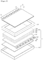
- FIG. 1 is an exploded perspective view showing a liquid crystal display according to the embodiment.
- FIG. 2 is a perspective view showing a light guide plate.
- FIG. 3 is a sectional view taken along line A-A' of FIG. 2 .
- FIG. 4 is a sectional view showing the light guide plate.
- FIG. 5 is a sectional view showing another light guide plate.
- FIG. 6 is a sectional view showing another light guide plate.
- FIG. 7 is a perspective view showing the light guide plate.
- FIG. 8 is a sectional view taken along line B-B' of FIG. 7 .
- FIG. 9 is a perspective view showing a light conversion 2. sheet.
- FIG. 10 is a sectional view taken along line C-C' of FIG. 9 .
- the liquid crystal display according to the embodiment includes a backlight unit 10 and a liquid crystal panel 20.
- the backlight unit 10 supplies light to the liquid crystal panel 30.
- the backlight unit 10 serves as a surface light source so that the light can be uniformly supplied to a bottom surface of the liquid crystal panel 20.
- the backlight unit 10 is disposed below the liquid crystal panel 20.
- the backlight unit 10 includes a bottom cover 100, a reflective sheet 300, a light source, for example, a plurality of light emitting diodes 400, a printed circuit board 401, a light guide plate 200, and a plurality of optical sheets 500.
- the bottom cover 100 receives the light guide plate 200, the light emitting diodes 400, the printed circuit board 401, the reflective sheet 300, and the optical sheets 500 therein.
- the reflective sheet 201 is disposed below the light guide plate 200.
- the reflective sheet 300 is disposed between the light guide plate 200 and a bottom surface of the bottom cover 100. The reflective sheet 300 reflects the light upward as the light is output downward from the bottom surface of the light guide plate 200.
- the light emitting diodes 400 serve as a light source for generating the light.
- the light emitting diodes 400 are disposed at one side of the light guide plate 200.
- the light generated from the light emitting diodes 400 is incident into the light guide plate 200 through the side of the light guide plate 200.
- the light emitting diodes 400 may include a blue light emitting diode generating the blue light or a UV light emitting diode generating the UV light.
- the light emitting diodes 400 may emit the blue light having the wavelength in the range of about 430nm to about 470nm or the UV light having the a wavelength in the range of about 300nm to abut 400nm.
- the light emitting diodes 400 are mounted on the printed circuit board 401.
- the light emitting diodes 400 may be disposed under the printed circuit board 401.
- the light emitting diodes 400 are driven by receiving a driving signal through the printed circuit board 401.
- the printed circuit board 401 is electrically connected to the light emitting diodes 400.
- the printed circuit board 401 may mount the light emitting diodes 400 thereon.
- the printed circuit board 401 is disposed in the bottom cover 100.
- the light guide plate 200 is disposed in the bottom cover 100.
- the light guide plate 200 is disposed on the reflective sheet 100.
- the light guide plate 200 supplies light received from the light emitting diode 300 upward by reflecting, refracting and scattering the light.
- the light guide plate 200 is disposed below the liquid crystal panel 200.
- the light guide plate 200 is disposed on the reflective sheet 300.
- the light guide plate 200 has a plate shape.
- the light guide plate 200 is transparent.
- a material used for the light guide plate 200 may include an acrylic resin formed by methyl acrylate, ethyl acrylate, cyclohexyl acrylate, or benzene acrylate.
- a guide part 210 may include polymer such as polymethylmethaacrylate ,PMMA, orpolycarbonate, PC.
- the light guide plate 200 may include glass.
- the glass used for the light guide plate 200 may include silicon oxide ,SiO2, titanum oxide TiO2, aluminum hydroxide Al(OH)3 or Zinc oxide ZnO.
- the light guide plate 200 may have a thickness in the range of about 0.5mm to about 1.5mm.
- a plurality of scattering parts 210 is formed on the light guide plate 200. That is, the scattering parts 210 are formed on at least one surface of the light guide plate 200.
- the scattering parts 210 may change a path of incident light. That is, the scattering parts 210 may serve as a light path changing part for changing the path of the incident light. In detail, the scattering parts 210 may scatter the incident light. In more detail, the scattering parts 210 may scatter the incident light upward.
- the scattering parts 210 configure a scattered pattern on a top surface of the light guide plate 200.
- the scattering parts 210 may be disposed on the top surface of the light guide plate 200.
- the scattering parts 210 may include protrusions which are formed on the top surface of the light guide plate 200.
- the scattering parts 210 may have a dot shape when viewed from a top side.
- a diameter R1 of each of scattering parts 210 may be equal to or greater than about 90 ⁇ mThe diameter R1 of each scattering part 210 may be in the range of about 90 ⁇ m to about 300 ⁇ m.In detail, the diameter R1 of each scattering part 210 may be in the range of about 100 ⁇ m to about 300 ⁇ m. In more detail, the diameter R1 of each scattering part 210 may be in the range of about 150 ⁇ m to about 250 ⁇ m.
- the scattering parts 210 are spaced apart from each other. In this case, a pitch P between the scattering parts 210 may be gradually reduced as the scattering parts 210 are located away from the light emitting diodes 400. That is, the scattering parts 210 may be densely disposed as the scattering parts 210 are located away from the light emitting diodes 400. Accordingly, the light guide plate 200 may uniformly supply light upward.
- the scattering part 210 includes a scattering protrusion 211 and a scattering groove 212.
- the scattering protrusion 211 may include a curved surface.
- a protruding part of the scattering protrusion 211 may have a curved surface as a whole.
- the scattering protrusion may have a semisphere shape.
- a diameter R2 of the scattering protrusion 211 may be in the range of about 80 ⁇ m to about 290 ⁇ m.
- a height of the scattering protrusion 211 may be in the range of about 40 ⁇ m to about 150 ⁇ m.
- the scattering groove 212 may be formed on the top surface of the light guide plate 200.
- the scattering groove 212 may be adjacent to the scattering protrusion 211.
- the scattering groove 212 may surround the scattering protrusion 211.
- the scattering groove 212 may extend around the scattering protrusion 211.
- the scattering groove 212 may have a closed loop shape when viewed from the top side.
- a width of each of the grooves 220 may be in the range of about 5 ⁇ m to about 10 ⁇ m.
- a depth of each of the grooves 220 may be in the range of about 2 ⁇ m to about 6 ⁇ m.
- the scattering parts 210 are provided on a bottom surface of the light guide plate 200. That is, the scattering parts 210 may directly face the reflective sheet 300.
- the scattering parts 210 may be provided on both of top and bottom surfaces of the light guide plate 200.
- a plurality of print scattering parts 220 may be provided in the light guide plate 200.
- the print scattering parts 220 may be printed on the top surface and are printed on the bottom surface of the light guide plate 200.
- the print scattering parts 220 may directly provided on the top surface and/or the bottom surface of the light guide plate 200.
- the print scattering parts 220 may be a pattern protruding from at least one surface of the light guide plate 200, for example, the top surface and/or the bottom surface of the light guide plate 200.
- a diameter R3 of each of the print scattering parts 220 is in the range of about 90 ⁇ m to about 300 ⁇ m.
- the diameter R3 of each of the print scattering parts 220 may be in the range of about 100 ⁇ m to about 300 ⁇ m.
- the diameter R3 of each of the print scattering parts 220 may be in the range of about 150 ⁇ m to about 250 ⁇ m.
- the print scattering parts 220 include a plurality of beads 221 and a printing part 222.
- the beads 221 may be transparent.
- the beads 221 may a high refractive index.
- the refractive index of the beads 221 may be in the range of about 1.6 to 2.2.
- the beads 221 include aluminum oxide Al2O3, or titanium oxide, TiO.
- a diameter of each of the beads 221 may be in the range of about 50nm to about 10 ⁇ m. In detail, the diameter of each of the beads 221 may be in the range of about 5 ⁇ m to about 10 ⁇ m.
- the printing part 222 includes a transparent resin.
- the printing part 222 receives the beads 221.
- the beads 221 may be inserted into the printing part 222.
- the printing part 22 may bond the beads 22 to the top surface or the bottom surface of the light guide plate 200.
- the printing part 222 may have a relatively high refractive index.
- a refractive index of the printing part 222 may be in the range of 1.2 to 1.4.
- the print scattering part 220 is farther away from the light emitting diode 400, an area of each printing scattering part 220gradually increases. Accordingly, the print scattering part 220 is farther away from the light emitting diode 400, so reduction in intensity of the light may be compensated.
- the optical sheets 500 are disposed on the light guide plate 200.
- the optical sheets 500 change or improve characteristics of light output from the top surface of the light guide plate 200 to supply the light to the liquid crystal panel 20.
- the optical sheets 500 includes a light conversion sheet 501, a diffusion sheet 502, a first prism sheet 503, and a second prism sheet 504.
- the light conversion sheet 501 is disposed on a light path between the light source and the liquid crystal panel 20.
- the conversion sheet 501 is be on the light guide plate 200.
- the light conversion sheet 501 may be interposed between the light guide plate 200 and the diffusion sheet 502.
- the light conversion sheet 501 may convert wavelength of incident light and supply the converted light upward.
- the light conversion sheet 501 may convert blue light supplied upward from the light guide plate 200 into green light and red light. That is, the light conversion sheet 501 may convert a part of the blue light into green light having a wavelength in the range of about 520nm to about 560nm, and convert another part of the blue light into red light having a wavelength in the range of about 630nm to about 660nm.
- the light conversion sheet 501 may convert UV ray output from the top surface of the light guide plate 200 into blue light, green light, and red light.
- the light conversion sheet 501 may convert a part of the UV ray into blue light having a wavelength in the range of about 430nm to about 470nm, and convert another part of the UV ray into green light having a wavelength in the range of about 520nm to about 560nm, and convert a still another part of the UV ray into red light having a wavelength in the range of about 630nm to about 660nm.
- light passing through the light conversion sheet 510 which is not converted and light converted by the light conversion sheet 501 form white light. That is, the blue light, the green light, and the red light are combined with each other so that the white light may be incident to the liquid crystal panel 20.
- the light conversion sheet 501 includes a lower substrate 510, an upper substrate 520, a light conversion layer 530, a lower reflection preventing layer 540, and an upper reflection preventing layer 550.
- the lower substrate 510 is disposed below the light conversion layer 530.
- the lower substrate 510 may be transparent and flexible.
- the lower substrate 510 may adhere to a bottom surface of the light conversion layer 530.
- a material use for the lower substrate 510 may include transparent polymer such as polyethyleneterephthalate PET.
- the upper substrate 520 is disposed on the light conversion layer 530.
- the upper substrate 520 may be transparent and flexible.
- the upper substrate 520 may adhere to the top surface of the light conversion layer 530.
- a material used for the upper substrate 520 may include transparent polymer such as PET.
- the light conversion layer 530 is sandwiched between the lower substrate 510 and the upper substrate 520.
- the lower substrate 510 and the upper substrate 520 support the light conversion layer 530.
- the lower substrate 510 and the upper substrate 520 protect the light conversion layer 530 from external physical impact.
- the lower substrate 510 and the upper substrate 520 have low oxygen permeability and low moisture permeability.
- the lower substrate 510 and the upper substrate 520 can protect the light conversion layer 530 from external chemical impact by moisture and/or oxygen.
- the light conversion layer 530 is interposed between the lower and upper substrates 510 and 520.
- the light conversion layer 530 may adhere to the top surface of the lower substrate 510, and adhere to the bottom surface of the upper substrate 520.
- the light conversion layer 530 includes a plurality of light conversion particles 531 and a host layer 532.
- the light conversion particles 531 are interposed between the lower and upper substrates 510 and 520.
- the light conversion particles 531 are uniformly distributed in the host layer 532, and the host layer 532 is interposed between the lower substrate 510 and the upper substrate 520.
- the light conversion particles 531 convert a wavelength of the light emitted from the light emitting diodes 400.
- the light conversion particles 531 receive light emitted from the light emitting diodes 400 to convert the a wavelength of the incident light.
- the light conversion particles 531 may convert the blue light emitted from the light emitting diodes 400 into the green light and the red light. That is, a part of the light conversion particles 531 may convert the blue light into green light having a wavelength in the range of about 520nm to about 560nm, and another part of the light conversion particles 531 may convert the blue light into red light having a wavelength in the range of about 630nm to about 660nm.
- the light conversion particles 531 may convert the UV ray emitted from the light emitting diodes 400 into the blue light, the green light, and the red light. That is, a part of the light conversion particles 531 may convert the UV ray into blue light having a wavelength in the range of about 430nm to about 470nm, and another part of the light conversion particles 531 may convert the UV ray into green light having a wavelength in the range of about 520nm to about 560nm. Still another part of the light conversion particles 531 may convert the UV ray into red light having a wavelength in the range of about 630nm to about 660nm.
- light conversion particles 531 for converting the blue light into green light and red light respectively may be used.
- light conversion particles 531 for converting the UV ray into blue light, green light, and red light respectively may be used.
- the light conversion particles 531 are a plurality of quantum dots, QD.
- the quantum dots may include core nano-crystals and shell nano-crystals surrounding the core nano-crystals.
- the quantum dots may include organic ligands bonded to the shell nano-crystals.
- the quantum dots may include an organic coating layer surrounding the shell nano-crystals.
- the shell nano-crystals may be prepared as at least two layers.
- the shell nano-crystals are formed on the surface of the core nano-crystals.
- the quantum dots lengthen a wavelength of the light incident into the core nano-crystals by using the shell nano-crystals forming a shell layer, thereby improving the light efficiency.
- the quantum dots may include at least one of a group-II compound semiconductor, a group-III compound semiconductor, a group-V compound semiconductor, and a group-VI compound semiconductor.
- the core nano-crystals may include CdSe, InGaP, CdTe, CdS, ZnSe, ZnTe, ZnS, HgTe or HgS.
- the shell nano-crystals may include CuZnS, CdSe, CdTe, CdS, ZnSe, ZnTe, ZnS, HgTe or HgS.
- the quantum dot may have a diameter of about 1nm to about 10nm.
- the wavelength of the light emitted from the quantum dots can be adjusted according to the size of the quantum dots.
- the organic ligand may include pyridine, mercapto alcohol, thiol, phosphine and phosphine oxide.
- the organic ligand may stabilize the unstable quantum dots after the synthesis process. Dangling bonds may be formed at the valence band and the quantum dots may be unstable due to the dangling bonds. However, since one end of the organic ligand is the non-bonding state, the one end of the organic ligand is bonded with the dangling bonds, thereby stabilizing the quantum dots.
- the size of the quantum dot is smaller than the Bohr radius of an exciton, which consists of an electron and a hole excited by light and electricity, the quantum confinement effect may occur, so that the quantum dot may have the discrete energy level.
- the size of the energy gap is changed.
- the charges are confined within the quantum dot, so that the light emitting efficiency can be improved.
- the fluorescent a wavelength of the quantum dot may vary depending on the size of the particles.
- the light has the shorter a wavelength as the size of the particle is reduced, so that the fluorescent light having the wavelength band of visible ray can be generated by adjusting the size of the particles.
- the quantum dot represents the extinction coefficient which is 100 to 1000 times higher than that of the general pigment and has the superior quantum yield as compared with the general pigment, so that strong fluorescent light can be generated.
- the quantum dots can be synthesized through the chemical wet scheme.
- the chemical wet scheme is to grow the particles by immersing the precursor material in the organic solvent. According to the chemical wet scheme, the quantum dots can be synthesized.
- the host layer 532 surrounds the light conversion particles 531. That is, the light conversion particles 531 are uniformly distributed in the host layer 532.
- the host layer 531 may include a polymer.
- the host layer 532 is transparent. That is, the host layer 532 may be formed by using a transparent polymer.
- the host layer 532 is interposed between the lower and upper substrates 510 and 520.
- the host layer 532 may adhere to the top surface of the lower substrate 510 and the bottom surface of the upper substrate 520.
- the sealing part 540 is disposed at the side of the light conversion layer 530.
- the sealing part 540 covers the side of the light conversion layer 530.
- the sealing part 540 can also be disposed at the sides of the lower substrate 510 and the upper substrate 520. In this case, the sealing part 540 covers the sides of the lower substrate 510 and the upper substrate 520.
- sealing part 540 may be bonded to the sides of the light conversion layer 530, the lower substrate 510 and the upper substrate 520. In addition, the sealing part 540 may closely adhere to the sides of the light conversion layer 530, the lower substrate 510 and the upper substrate 520.
- the sealing part 540 can seal the side of the wavelength conversion layer 530. That is, the sealing part 540 may serve as a protective part for protecting the wavelength conversion layer 530 from the external chemical impact.
- the liquid crystal panel 20 is disposed on the optical sheets 500.
- the liquid crystal panel 20 is disposed on the panel guide 23.
- the liquid crystal panel 20 may be guided by the panel guide 23.
- the liquid crystal panel 20 displays images by adjusting intensity of light passing through the liquid crystal panel 20.
- the liquid crystal panel 20 is a display panel for displaying the images by using the light emitted from the backlight unit 10.
- the liquid crystal panel 20 includes a TFT substrate 21, a color filter substrate 22 and a liquid crystal layer interposed between the two substrates.
- the liquid crystal panel 20 includes polarizing filters.
- the TFT substrate 21 includes a plurality of gate lines and a plurality of data lines crossing the gate lines to define pixels and a thin film transistor, TFT, is provided at each cross section such that the thin film transistor TFT can be connected to a pixel electrode of the pixel in one-to-one correspondence.
- the color filter substrate 22 includes color filters having R, G and B colors corresponding to the pixels, a black matrix covering the gate lines, data lines and thin film transistors within the limit of the color filters, and a common electrode covering the above elements.
- a driving PCB 25 is provided at an outer peripheral portion of the liquid crystal panel 210 to supply driving signals to the gate lines and data lines.
- the driving PCB 25 is electrically connected to the liquid crystal panel 20 by a COF (chip on film) 24.
- the COF 24 may be replaced with a TCP (tape carrier package).
- the liquid crystal display according to the embodiment disposes the light conversion member on the light guide plate 200 and the scattering parts 210 have a large diameter in the range of about 90 ⁇ m to about 300 ⁇ m.
- the light conversion member includes the light conversion particles.
- the light conversion particles may randomly change a light path while convert a wavelength of incident light. That is, the light conversion particles may also perform a scattering function.
- the scattering parts 210 have a large diameter, because the light conversion member has the scattering function, the whole brightness uniformity is not reduced.
- the scattering parts 210 have a large diameter so that the whole brightness may be increased.
- the display device can represent improved brightness without reducing brightness uniformity.
- any reference in this specification to "one embodiment,” “an embodiment,” “example embodiment,” etc. means that a particular feature, structure, or characteristic described in connection with the embodiment is included in at least one embodiment of the invention.
- the appearances of such phrases in various places in the specification are not necessarily all referring to the same embodiment.
- a light conversion sheet including a CdSe/ZnS quantum dot having a diameter of about 2nm was disposed on a top surface of a light guide plate in which scattering parts having a diameter of about 150 ⁇ m were provided, and then light was emitted to a side of the light guide plate using a blue light emitting diode.
- Comparative Example is similar to Experimental Example except that the scattering parts having a diameter of about 25 ⁇ m were provided on the light guide plate.
- Brightness uniformity of the Experimental Example is substantially the same as that of the Comparative Example and brightness of the Experimental Example was improved by about 2% as compared with that of the Comparative Example.
Landscapes
- Physics & Mathematics (AREA)
- General Physics & Mathematics (AREA)
- Optics & Photonics (AREA)
- Nonlinear Science (AREA)
- Mathematical Physics (AREA)
- Chemical & Material Sciences (AREA)
- Crystallography & Structural Chemistry (AREA)
- Planar Illumination Modules (AREA)
Claims (8)
- Un dispositif d'affichage comprenant :une plaque (200) de guidage de lumière ayant une surface supérieure, une surface inférieure et des surfaces latérales ;une source de lumière comprenant une pluralité de diodes (400) émettrices de lumière et étant disposée latéralement par rapport à la plaque (200) de guidage de lumière pour émettre de la lumière dans au moins une surface latérale de la plaque (200) de guidage de lumière ;un élément (501) de conversion de lumière sur la plaque (200) de guidage de lumière ;une feuille réfléchissante (300) sous la plaque (200) de guidage de lumière ;un panneau d'affichage (20) sur l'élément de conversion de lumière ; etune pluralité de parties (220) de diffusion d'impression sur la surface inférieure de la plaque (200) de guidage de lumière,la plaque (200) de guidage de lumière étant prévue entre l'élément de conversion de lumière et la feuille réfléchissante,les parties (220) de diffusion d'impression étant prévues entre la surface inférieure de la plaque (200) de guidage de lumière et la feuille réfléchissante,caractérisé en ce que chaque partie de la pluralité de parties (220) de diffusion d'impression a un diamètre allant de 90 µm à 300 µm, et
l'élément (501) de conversion de lumière comprenant :un substrat inférieur (510) :une couche (530) de conversion de lumière sur le substrat inférieur (510) ; etun substrat supérieur (520) sur la couche de conversion de lumière, la couche (530) de conversion de lumière comprenant :une couche hôte (532) ; etune pluralité de points quantiques (531) dispersés dans la couche hôte (532),chacune des parties de diffusion d'impression comprenant une pluralité de billes, et de la résine qui reçoit les billes,les billes comprenant de l'oxyde d'aluminium, Al2O3, ou de l'oxyde de titane, TiO, et en outre une surface de chaque partie de la pluralité des parties de diffusion augmentant progressivement au fur et à mesure que sa distance par rapport aux diodes émettrices de lumière augmente. - Le dispositif d'affichage selon la revendication 1, dans lequel les billes sont en contact direct avec la résine de chaque partie de diffusion.
- Le dispositif d'affichage selon la revendication 1, comprenant en outre des parties de diffusion d'impression prévues sur la surface supérieure de la plaque (200) de guidage de lumière.
- Le dispositif d'affichage selon la revendication 3, dans lequel les parties de diffusion supérieures comportent une pluralité de billes.
- Le dispositif d'affichage selon la revendication 4, dans lequel un diamètre de chacune des billes des parties de diffusion supérieures est compris entre 50 nm et 10 µm.
- Le dispositif d'affichage selon la revendication 1, dans lequel au moins un parmi le substrat inférieur et le substrat supérieur comprend du polyéthylène téréphtalate, PET.
- Le dispositif d'affichage selon la revendication 1, dans lequel l'élément de conversion de lumière comprend en outre au moins une parmi une couche inférieure antireflet et d'une couche supérieure antireflet.
- Le dispositif d'affichage selon la revendication 1, dans lequel un indice de réfraction des billes et de la résine sont différents.
Applications Claiming Priority (3)
| Application Number | Priority Date | Filing Date | Title |
|---|---|---|---|
| KR1020110131365A KR101664507B1 (ko) | 2011-12-08 | 2011-12-08 | 표시장치 |
| EP12856122.2A EP2788816A4 (fr) | 2011-12-08 | 2012-11-23 | Dispositif d'affichage |
| PCT/KR2012/009995 WO2013085187A1 (fr) | 2011-12-08 | 2012-11-23 | Dispositif d'affichage |
Related Parent Applications (1)
| Application Number | Title | Priority Date | Filing Date |
|---|---|---|---|
| EP12856122.2A Division EP2788816A4 (fr) | 2011-12-08 | 2012-11-23 | Dispositif d'affichage |
Publications (2)
| Publication Number | Publication Date |
|---|---|
| EP3267246A1 EP3267246A1 (fr) | 2018-01-10 |
| EP3267246B1 true EP3267246B1 (fr) | 2021-09-29 |
Family
ID=48574499
Family Applications (2)
| Application Number | Title | Priority Date | Filing Date |
|---|---|---|---|
| EP17184709.8A Active EP3267246B1 (fr) | 2011-12-08 | 2012-11-23 | Afficheur |
| EP12856122.2A Ceased EP2788816A4 (fr) | 2011-12-08 | 2012-11-23 | Dispositif d'affichage |
Family Applications After (1)
| Application Number | Title | Priority Date | Filing Date |
|---|---|---|---|
| EP12856122.2A Ceased EP2788816A4 (fr) | 2011-12-08 | 2012-11-23 | Dispositif d'affichage |
Country Status (6)
| Country | Link |
|---|---|
| US (2) | US9494723B2 (fr) |
| EP (2) | EP3267246B1 (fr) |
| KR (1) | KR101664507B1 (fr) |
| CN (2) | CN104081264A (fr) |
| TW (1) | TWI588548B (fr) |
| WO (1) | WO2013085187A1 (fr) |
Families Citing this family (17)
| Publication number | Priority date | Publication date | Assignee | Title |
|---|---|---|---|---|
| JP6002071B2 (ja) * | 2013-03-26 | 2016-10-05 | 株式会社東芝 | 照明装置及び導光部材 |
| JP2015046328A (ja) * | 2013-08-28 | 2015-03-12 | 富士フイルム株式会社 | 導光板、これを含むバックライトユニットおよび液晶表示装置、ならびに光学シート |
| KR20150064463A (ko) * | 2013-12-03 | 2015-06-11 | 삼성디스플레이 주식회사 | 발광다이오드 패키지 및 이를 광원으로 갖는 표시장치 |
| TWI518386B (zh) * | 2014-04-02 | 2016-01-21 | 群創光電股份有限公司 | 顯示裝置 |
| JP5843024B1 (ja) | 2014-08-22 | 2016-01-13 | 大日本印刷株式会社 | 表示装置 |
| WO2016027789A1 (fr) * | 2014-08-22 | 2016-02-25 | Nsマテリアルズ株式会社 | Élément de conversion de longueur d'onde, et dispositif électroluminescent, élément électroluminescent, dispositif source de lumière et dispositif d'affichage l'utilisant |
| WO2016130731A1 (fr) * | 2015-02-13 | 2016-08-18 | Corning Incorporated | Filtres angulaires et dispositifs d'affichage comprenant ces derniers |
| KR102312522B1 (ko) * | 2015-06-11 | 2021-10-15 | 삼성디스플레이 주식회사 | 표시 장치 |
| KR101608963B1 (ko) * | 2015-06-19 | 2016-04-04 | (주)코이즈 | 복합 패턴 도광판 및 그 제조방법 |
| KR20170004205A (ko) * | 2015-07-01 | 2017-01-11 | 엘지전자 주식회사 | 도광판 및 이를 포함하는 면광원 장치 |
| KR102527931B1 (ko) * | 2016-08-02 | 2023-05-03 | 삼성디스플레이 주식회사 | 백라이트 유닛 및 이를 포함하는 표시 장치 |
| CN107065299A (zh) * | 2016-12-31 | 2017-08-18 | 惠科股份有限公司 | 背光模块的制造方法 |
| US10495923B2 (en) | 2017-07-24 | 2019-12-03 | Wuhan China Star Optoelectronics Technology Co., Ltd. | Backlight module and liquid crystal display |
| CN107193077A (zh) * | 2017-07-24 | 2017-09-22 | 武汉华星光电技术有限公司 | 背光模块及液晶显示器 |
| KR102436671B1 (ko) * | 2018-01-03 | 2022-08-29 | 삼성디스플레이 주식회사 | 백라이트 유닛 및 이를 포함하는 표시 장치 |
| US20190219874A1 (en) * | 2018-01-16 | 2019-07-18 | Huizhou China Star Optoelectronics Technology Co., Ltd. | Backlight module and display device |
| CN110673244B (zh) * | 2019-09-27 | 2021-02-02 | 南京贝迪新材料科技股份有限公司 | 一种量子点复合增亮膜及其制备方法 |
Family Cites Families (59)
| Publication number | Priority date | Publication date | Assignee | Title |
|---|---|---|---|---|
| WO2001066997A2 (fr) * | 2000-03-06 | 2001-09-13 | Teledyne Lighting And Display Products, Inc. | Appareil d'eclairage dote d'une couche a points quantiques |
| CN2496052Y (zh) * | 2001-04-13 | 2002-06-19 | 宋义 | 改进的均匀高效率侧发光背光源 |
| CN2586980Y (zh) * | 2002-11-23 | 2003-11-19 | 鸿富锦精密工业(深圳)有限公司 | 背光模块 |
| CN2588387Y (zh) * | 2002-12-13 | 2003-11-26 | 鸿富锦精密工业(深圳)有限公司 | 导光板和平面发光装置 |
| TWI280427B (en) * | 2003-01-29 | 2007-05-01 | Hon Hai Prec Ind Co Ltd | Back light module |
| CN100376950C (zh) * | 2003-11-13 | 2008-03-26 | 鸿富锦精密工业(深圳)有限公司 | 背光模组及其导光板 |
| TWI291770B (en) * | 2003-11-14 | 2007-12-21 | Hon Hai Prec Ind Co Ltd | Surface light source device and light emitting diode |
| TWI283777B (en) | 2003-11-14 | 2007-07-11 | Hon Hai Prec Ind Co Ltd | Light guide plate and method for making it and backlight module using it |
| TWI275858B (en) * | 2003-11-14 | 2007-03-11 | Hon Hai Prec Ind Co Ltd | Light guide plate |
| TW200517238A (en) * | 2003-11-21 | 2005-06-01 | Hon Hai Prec Ind Co Ltd | A light guide plate injection mold |
| TW200528849A (en) * | 2004-02-27 | 2005-09-01 | Hon Hai Prec Ind Co Ltd | Light guide plate |
| TWI300494B (en) * | 2004-07-23 | 2008-09-01 | Hon Hai Prec Ind Co Ltd | Light guiding plate and backlight module using the same |
| TWI299412B (en) * | 2004-08-27 | 2008-08-01 | Hon Hai Prec Ind Co Ltd | Light guide plate and backlight module using the same |
| TWI276882B (en) | 2004-12-10 | 2007-03-21 | Hon Hai Prec Ind Co Ltd | Light guide plate and backlight module |
| US7416309B2 (en) * | 2004-12-30 | 2008-08-26 | 3M Innovative Properties Company | Optical film having a surface with rounded structures |
| JP4329736B2 (ja) * | 2005-07-04 | 2009-09-09 | セイコーエプソン株式会社 | 光学基板、面状照明装置、電気光学装置 |
| KR20070108794A (ko) | 2006-05-08 | 2007-11-13 | 미래나노텍(주) | 광학 시트 및 상기 광학 시트가 구비된 액정표시장치의백라이트 어셈블리 |
| CN100516642C (zh) * | 2006-08-03 | 2009-07-22 | 哈利盛东芝照明株式会社 | 中空式平板照明装置 |
| TW200817777A (en) | 2006-08-03 | 2008-04-16 | Harison Toshiba Lighting Corp | Hollow type flat lighting system |
| US7661862B2 (en) * | 2006-12-07 | 2010-02-16 | Skc Haas Display Films Co., Ltd. | LCD display backlight using elongated illuminators |
| US8456590B2 (en) * | 2007-01-09 | 2013-06-04 | Dai Nippon Printing Co., Ltd. | Optical sheet, surface light source and display device |
| TWM322627U (en) * | 2007-06-06 | 2007-11-21 | Acpa Energy Conversion Devices | Passive light-emitting module whose visible lights are excited from the ultraviolet |
| CN101349776A (zh) * | 2007-07-18 | 2009-01-21 | 宣茂科技股份有限公司 | 导光板 |
| US20090034230A1 (en) * | 2007-07-31 | 2009-02-05 | Luminus Devices, Inc. | Illumination assembly including wavelength converting material having spatially varying density |
| US8434909B2 (en) * | 2007-10-09 | 2013-05-07 | Flex Lighting Ii, Llc | Light emitting display with light mixing within a film |
| US8269420B2 (en) * | 2007-10-12 | 2012-09-18 | Sony Corporation | Illuminating device having fluorescent lamp, display apparatus including the same, and light-diffusing film |
| US20090122227A1 (en) * | 2007-11-08 | 2009-05-14 | Rohm And Haas Denmark Finance A/S | Integrated backlight illumination assembly |
| CN101903816A (zh) * | 2007-12-17 | 2010-12-01 | 日立化成工业株式会社 | 可见光波导用光波导 |
| KR101460155B1 (ko) * | 2008-01-15 | 2014-11-10 | 삼성전자주식회사 | 백라이트 유닛 및 이를 구비한 액정 디스플레이 장치 |
| TWM341811U (en) | 2008-02-18 | 2008-10-01 | Kismart Corp | Light source module with shared wavelength converting structure |
| CN101280190A (zh) * | 2008-05-26 | 2008-10-08 | 南开大学 | 水相合成稳定的GSH-CdTeSe合金量子点的方法 |
| CN101614839A (zh) | 2008-06-26 | 2009-12-30 | 胜华科技股份有限公司 | 背光模块及导光板 |
| CN102084507B (zh) * | 2008-07-01 | 2016-01-20 | 皇家飞利浦电子股份有限公司 | 具有降低的未转换光发射的波长转换发光二极管 |
| DE102008031996A1 (de) * | 2008-07-07 | 2010-02-18 | Osram Gesellschaft mit beschränkter Haftung | Strahlungsemittierende Vorrichtung |
| CN101634726B (zh) * | 2008-07-21 | 2012-06-13 | 鸿富锦精密工业(深圳)有限公司 | 导光板及其制造方法,以及采用该导光板的背光模组 |
| CN101685180A (zh) | 2008-09-27 | 2010-03-31 | 上海边光实业有限公司 | 一种有利于光线均匀分布的导光板 |
| JP2010096916A (ja) * | 2008-10-15 | 2010-04-30 | Keiwa Inc | 光学シート及びこれを用いたバックライトユニット |
| TWI410713B (zh) | 2008-11-06 | 2013-10-01 | Ind Tech Res Inst | 背光模組與液晶顯示器 |
| CN101856684A (zh) * | 2009-04-08 | 2010-10-13 | 鸿富锦精密工业(深圳)有限公司 | 镜片、镜片阵列及其制造方法 |
| KR20090054415A (ko) * | 2009-04-24 | 2009-05-29 | 미래나노텍(주) | 광학 시트 및 상기 광학 시트가 구비된 액정표시장치의 백라이트 어셈블리 |
| CN101870151A (zh) * | 2009-04-27 | 2010-10-27 | 鸿富锦精密工业(深圳)有限公司 | 光学元件的制造方法及压印模具 |
| US8783898B2 (en) * | 2009-05-01 | 2014-07-22 | Abl Ip Holding Llc | Light emitting devices and applications thereof |
| KR100943233B1 (ko) * | 2009-06-03 | 2010-02-18 | 주식회사 우즈필 | 확산잉크 조성물 |
| KR20110006811A (ko) | 2009-07-15 | 2011-01-21 | 삼성전자주식회사 | 칼라 필터 어레이 및 이를 포함하는 이미지 센서와 전자 장치 |
| KR20110022970A (ko) * | 2009-08-28 | 2011-03-08 | 엘지이노텍 주식회사 | 표시장치 |
| DE112010004660T5 (de) * | 2009-12-02 | 2012-10-11 | Mitsubishi Electric Corporation | Flüssigkristalldisplayeinrichtung |
| WO2011086719A1 (fr) * | 2010-01-15 | 2011-07-21 | 凸版印刷株式会社 | Corps de guidage de lumière, structure de dissimulation, et dispositif d'éclairage et appareil d'affichage le comportant |
| JP5068865B2 (ja) * | 2010-04-09 | 2012-11-07 | シャープ株式会社 | 光源モジュール、およびそれを備えた電子機器 |
| TWI474082B (zh) * | 2010-04-15 | 2015-02-21 | Mitsubishi Electric Corp | 背光裝置及液晶顯示裝置 |
| JP2013525955A (ja) * | 2010-04-16 | 2013-06-20 | フレックス ライティング 2,エルエルシー | フィルムベースのライトガイドを備える照明デバイス |
| CN101894678B (zh) * | 2010-06-07 | 2012-06-06 | 天津大学 | 海绵状量子点太阳能电池及其制备方法 |
| KR20120007944A (ko) * | 2010-07-15 | 2012-01-25 | 주식회사 엘지화학 | 광학 성능이 향상된 광학필름 및 이를 포함하는 백라이트 유닛 |
| JP5129379B2 (ja) * | 2010-09-17 | 2013-01-30 | 日東電工株式会社 | 光拡散素子 |
| JP5309111B2 (ja) * | 2010-10-29 | 2013-10-09 | 富士フイルム株式会社 | 光拡散フィルム、偏光板、画像表示装置、及び光拡散フィルムの製造方法 |
| KR102098682B1 (ko) * | 2010-11-10 | 2020-05-22 | 나노시스, 인크. | 양자 도트 필름들, 조명 디바이스들, 및 조명 방법들 |
| US9244284B2 (en) * | 2011-03-15 | 2016-01-26 | 3M Innovative Properties Company | Microreplicated film for autostereoscopic displays |
| TW201128245A (en) | 2011-03-31 | 2011-08-16 | Global Lighting Technologies Taiwan Inc | Light-guide plate and the manufacturing method |
| KR101673627B1 (ko) * | 2011-08-31 | 2016-11-07 | 엘지이노텍 주식회사 | 광학 부재 및 표시장치 |
| TW201317677A (zh) * | 2011-10-24 | 2013-05-01 | Hon Hai Prec Ind Co Ltd | 背光模組 |
-
2011
- 2011-12-08 KR KR1020110131365A patent/KR101664507B1/ko active IP Right Grant
-
2012
- 2012-11-23 CN CN201280068353.4A patent/CN104081264A/zh active Pending
- 2012-11-23 EP EP17184709.8A patent/EP3267246B1/fr active Active
- 2012-11-23 EP EP12856122.2A patent/EP2788816A4/fr not_active Ceased
- 2012-11-23 WO PCT/KR2012/009995 patent/WO2013085187A1/fr active Application Filing
- 2012-11-23 CN CN201710635861.0A patent/CN107450230A/zh active Pending
- 2012-11-23 US US14/362,838 patent/US9494723B2/en active Active
- 2012-11-30 TW TW101145016A patent/TWI588548B/zh active
-
2016
- 2016-10-05 US US15/286,387 patent/US9606284B2/en active Active
Also Published As
| Publication number | Publication date |
|---|---|
| EP3267246A1 (fr) | 2018-01-10 |
| US20140307465A1 (en) | 2014-10-16 |
| KR20130064650A (ko) | 2013-06-18 |
| KR101664507B1 (ko) | 2016-10-10 |
| US20170023728A1 (en) | 2017-01-26 |
| WO2013085187A1 (fr) | 2013-06-13 |
| TWI588548B (zh) | 2017-06-21 |
| US9494723B2 (en) | 2016-11-15 |
| EP2788816A4 (fr) | 2015-11-18 |
| EP2788816A1 (fr) | 2014-10-15 |
| CN104081264A (zh) | 2014-10-01 |
| CN107450230A (zh) | 2017-12-08 |
| TW201331647A (zh) | 2013-08-01 |
| US9606284B2 (en) | 2017-03-28 |
Similar Documents
| Publication | Publication Date | Title |
|---|---|---|
| EP3267246B1 (fr) | Afficheur | |
| US9625639B2 (en) | Optical member and display device including the same | |
| US9529138B2 (en) | Display device | |
| EP2699959B1 (fr) | Élément optique | |
| US10215366B2 (en) | Optical member and display device including the same | |
| EP2937720B1 (fr) | Dispositif d'affichage équipé d'un élément de conversion de longueur d'onde optique | |
| KR101251815B1 (ko) | 광학 시트 및 이를 포함하는 표시장치 | |
| KR101673627B1 (ko) | 광학 부재 및 표시장치 | |
| CN105988243B (zh) | 光学构件、背光单元以及显示装置 | |
| US9594203B2 (en) | Optical member, display device having the same and method for fabricating the same | |
| KR20130000508A (ko) | 표시장치 | |
| KR101814807B1 (ko) | 광학 부재 및 이를 포함하는 표시장치 | |
| KR20150102139A (ko) | 백라이트 유닛 및 이를 포함하는 액정표시장치 | |
| KR101882199B1 (ko) | 광학 부재, 이를 포함하는 표시장치 및 이의 제조방법 | |
| KR101725012B1 (ko) | 표시장치 | |
| KR101795046B1 (ko) | 표시장치 |
Legal Events
| Date | Code | Title | Description |
|---|---|---|---|
| PUAI | Public reference made under article 153(3) epc to a published international application that has entered the european phase |
Free format text: ORIGINAL CODE: 0009012 |
|
| STAA | Information on the status of an ep patent application or granted ep patent |
Free format text: STATUS: THE APPLICATION HAS BEEN PUBLISHED |
|
| AC | Divisional application: reference to earlier application |
Ref document number: 2788816 Country of ref document: EP Kind code of ref document: P |
|
| AK | Designated contracting states |
Kind code of ref document: A1 Designated state(s): AL AT BE BG CH CY CZ DE DK EE ES FI FR GB GR HR HU IE IS IT LI LT LU LV MC MK MT NL NO PL PT RO RS SE SI SK SM TR |
|
| STAA | Information on the status of an ep patent application or granted ep patent |
Free format text: STATUS: REQUEST FOR EXAMINATION WAS MADE |
|
| 17P | Request for examination filed |
Effective date: 20180515 |
|
| RBV | Designated contracting states (corrected) |
Designated state(s): AL AT BE BG CH CY CZ DE DK EE ES FI FR GB GR HR HU IE IS IT LI LT LU LV MC MK MT NL NO PL PT RO RS SE SI SK SM TR |
|
| STAA | Information on the status of an ep patent application or granted ep patent |
Free format text: STATUS: EXAMINATION IS IN PROGRESS |
|
| 17Q | First examination report despatched |
Effective date: 20190904 |
|
| STAA | Information on the status of an ep patent application or granted ep patent |
Free format text: STATUS: EXAMINATION IS IN PROGRESS |
|
| GRAP | Despatch of communication of intention to grant a patent |
Free format text: ORIGINAL CODE: EPIDOSNIGR1 |
|
| STAA | Information on the status of an ep patent application or granted ep patent |
Free format text: STATUS: GRANT OF PATENT IS INTENDED |
|
| INTG | Intention to grant announced |
Effective date: 20210430 |
|
| GRAS | Grant fee paid |
Free format text: ORIGINAL CODE: EPIDOSNIGR3 |
|
| GRAA | (expected) grant |
Free format text: ORIGINAL CODE: 0009210 |
|
| STAA | Information on the status of an ep patent application or granted ep patent |
Free format text: STATUS: THE PATENT HAS BEEN GRANTED |
|
| AC | Divisional application: reference to earlier application |
Ref document number: 2788816 Country of ref document: EP Kind code of ref document: P |
|
| AK | Designated contracting states |
Kind code of ref document: B1 Designated state(s): AL AT BE BG CH CY CZ DE DK EE ES FI FR GB GR HR HU IE IS IT LI LT LU LV MC MK MT NL NO PL PT RO RS SE SI SK SM TR |
|
| REG | Reference to a national code |
Ref country code: GB Ref legal event code: FG4D |
|
| REG | Reference to a national code |
Ref country code: CH Ref legal event code: EP Ref country code: AT Ref legal event code: REF Ref document number: 1434721 Country of ref document: AT Kind code of ref document: T Effective date: 20211015 |
|
| REG | Reference to a national code |
Ref country code: DE Ref legal event code: R096 Ref document number: 602012076829 Country of ref document: DE |
|
| REG | Reference to a national code |
Ref country code: IE Ref legal event code: FG4D |
|
| REG | Reference to a national code |
Ref country code: LT Ref legal event code: MG9D |
|
| PG25 | Lapsed in a contracting state [announced via postgrant information from national office to epo] |
Ref country code: LT Free format text: LAPSE BECAUSE OF FAILURE TO SUBMIT A TRANSLATION OF THE DESCRIPTION OR TO PAY THE FEE WITHIN THE PRESCRIBED TIME-LIMIT Effective date: 20210929 Ref country code: BG Free format text: LAPSE BECAUSE OF FAILURE TO SUBMIT A TRANSLATION OF THE DESCRIPTION OR TO PAY THE FEE WITHIN THE PRESCRIBED TIME-LIMIT Effective date: 20211229 Ref country code: HR Free format text: LAPSE BECAUSE OF FAILURE TO SUBMIT A TRANSLATION OF THE DESCRIPTION OR TO PAY THE FEE WITHIN THE PRESCRIBED TIME-LIMIT Effective date: 20210929 Ref country code: FI Free format text: LAPSE BECAUSE OF FAILURE TO SUBMIT A TRANSLATION OF THE DESCRIPTION OR TO PAY THE FEE WITHIN THE PRESCRIBED TIME-LIMIT Effective date: 20210929 Ref country code: NO Free format text: LAPSE BECAUSE OF FAILURE TO SUBMIT A TRANSLATION OF THE DESCRIPTION OR TO PAY THE FEE WITHIN THE PRESCRIBED TIME-LIMIT Effective date: 20211229 Ref country code: SE Free format text: LAPSE BECAUSE OF FAILURE TO SUBMIT A TRANSLATION OF THE DESCRIPTION OR TO PAY THE FEE WITHIN THE PRESCRIBED TIME-LIMIT Effective date: 20210929 Ref country code: RS Free format text: LAPSE BECAUSE OF FAILURE TO SUBMIT A TRANSLATION OF THE DESCRIPTION OR TO PAY THE FEE WITHIN THE PRESCRIBED TIME-LIMIT Effective date: 20210929 |
|
| REG | Reference to a national code |
Ref country code: NL Ref legal event code: MP Effective date: 20210929 |
|
| REG | Reference to a national code |
Ref country code: AT Ref legal event code: MK05 Ref document number: 1434721 Country of ref document: AT Kind code of ref document: T Effective date: 20210929 |
|
| PG25 | Lapsed in a contracting state [announced via postgrant information from national office to epo] |
Ref country code: LV Free format text: LAPSE BECAUSE OF FAILURE TO SUBMIT A TRANSLATION OF THE DESCRIPTION OR TO PAY THE FEE WITHIN THE PRESCRIBED TIME-LIMIT Effective date: 20210929 Ref country code: GR Free format text: LAPSE BECAUSE OF FAILURE TO SUBMIT A TRANSLATION OF THE DESCRIPTION OR TO PAY THE FEE WITHIN THE PRESCRIBED TIME-LIMIT Effective date: 20211230 |
|
| PG25 | Lapsed in a contracting state [announced via postgrant information from national office to epo] |
Ref country code: AT Free format text: LAPSE BECAUSE OF FAILURE TO SUBMIT A TRANSLATION OF THE DESCRIPTION OR TO PAY THE FEE WITHIN THE PRESCRIBED TIME-LIMIT Effective date: 20210929 |
|
| PG25 | Lapsed in a contracting state [announced via postgrant information from national office to epo] |
Ref country code: IS Free format text: LAPSE BECAUSE OF FAILURE TO SUBMIT A TRANSLATION OF THE DESCRIPTION OR TO PAY THE FEE WITHIN THE PRESCRIBED TIME-LIMIT Effective date: 20220129 Ref country code: SK Free format text: LAPSE BECAUSE OF FAILURE TO SUBMIT A TRANSLATION OF THE DESCRIPTION OR TO PAY THE FEE WITHIN THE PRESCRIBED TIME-LIMIT Effective date: 20210929 Ref country code: RO Free format text: LAPSE BECAUSE OF FAILURE TO SUBMIT A TRANSLATION OF THE DESCRIPTION OR TO PAY THE FEE WITHIN THE PRESCRIBED TIME-LIMIT Effective date: 20210929 Ref country code: PT Free format text: LAPSE BECAUSE OF FAILURE TO SUBMIT A TRANSLATION OF THE DESCRIPTION OR TO PAY THE FEE WITHIN THE PRESCRIBED TIME-LIMIT Effective date: 20220131 Ref country code: PL Free format text: LAPSE BECAUSE OF FAILURE TO SUBMIT A TRANSLATION OF THE DESCRIPTION OR TO PAY THE FEE WITHIN THE PRESCRIBED TIME-LIMIT Effective date: 20210929 Ref country code: NL Free format text: LAPSE BECAUSE OF FAILURE TO SUBMIT A TRANSLATION OF THE DESCRIPTION OR TO PAY THE FEE WITHIN THE PRESCRIBED TIME-LIMIT Effective date: 20210929 Ref country code: ES Free format text: LAPSE BECAUSE OF FAILURE TO SUBMIT A TRANSLATION OF THE DESCRIPTION OR TO PAY THE FEE WITHIN THE PRESCRIBED TIME-LIMIT Effective date: 20210929 Ref country code: EE Free format text: LAPSE BECAUSE OF FAILURE TO SUBMIT A TRANSLATION OF THE DESCRIPTION OR TO PAY THE FEE WITHIN THE PRESCRIBED TIME-LIMIT Effective date: 20210929 Ref country code: CZ Free format text: LAPSE BECAUSE OF FAILURE TO SUBMIT A TRANSLATION OF THE DESCRIPTION OR TO PAY THE FEE WITHIN THE PRESCRIBED TIME-LIMIT Effective date: 20210929 Ref country code: AL Free format text: LAPSE BECAUSE OF FAILURE TO SUBMIT A TRANSLATION OF THE DESCRIPTION OR TO PAY THE FEE WITHIN THE PRESCRIBED TIME-LIMIT Effective date: 20210929 |
|
| PG25 | Lapsed in a contracting state [announced via postgrant information from national office to epo] |
Ref country code: MC Free format text: LAPSE BECAUSE OF FAILURE TO SUBMIT A TRANSLATION OF THE DESCRIPTION OR TO PAY THE FEE WITHIN THE PRESCRIBED TIME-LIMIT Effective date: 20210929 |
|
| REG | Reference to a national code |
Ref country code: DE Ref legal event code: R097 Ref document number: 602012076829 Country of ref document: DE Ref country code: CH Ref legal event code: PL |
|
| PG25 | Lapsed in a contracting state [announced via postgrant information from national office to epo] |
Ref country code: LU Free format text: LAPSE BECAUSE OF NON-PAYMENT OF DUE FEES Effective date: 20211123 Ref country code: DK Free format text: LAPSE BECAUSE OF FAILURE TO SUBMIT A TRANSLATION OF THE DESCRIPTION OR TO PAY THE FEE WITHIN THE PRESCRIBED TIME-LIMIT Effective date: 20210929 Ref country code: BE Free format text: LAPSE BECAUSE OF NON-PAYMENT OF DUE FEES Effective date: 20211130 |
|
| REG | Reference to a national code |
Ref country code: BE Ref legal event code: MM Effective date: 20211130 |
|
| PLBE | No opposition filed within time limit |
Free format text: ORIGINAL CODE: 0009261 |
|
| STAA | Information on the status of an ep patent application or granted ep patent |
Free format text: STATUS: NO OPPOSITION FILED WITHIN TIME LIMIT |
|
| GBPC | Gb: european patent ceased through non-payment of renewal fee |
Effective date: 20211229 |
|
| 26N | No opposition filed |
Effective date: 20220630 |
|
| PG25 | Lapsed in a contracting state [announced via postgrant information from national office to epo] |
Ref country code: IE Free format text: LAPSE BECAUSE OF NON-PAYMENT OF DUE FEES Effective date: 20211123 Ref country code: GB Free format text: LAPSE BECAUSE OF NON-PAYMENT OF DUE FEES Effective date: 20211229 |
|
| PG25 | Lapsed in a contracting state [announced via postgrant information from national office to epo] |
Ref country code: SI Free format text: LAPSE BECAUSE OF FAILURE TO SUBMIT A TRANSLATION OF THE DESCRIPTION OR TO PAY THE FEE WITHIN THE PRESCRIBED TIME-LIMIT Effective date: 20210929 Ref country code: FR Free format text: LAPSE BECAUSE OF NON-PAYMENT OF DUE FEES Effective date: 20211129 |
|
| PG25 | Lapsed in a contracting state [announced via postgrant information from national office to epo] |
Ref country code: IT Free format text: LAPSE BECAUSE OF FAILURE TO SUBMIT A TRANSLATION OF THE DESCRIPTION OR TO PAY THE FEE WITHIN THE PRESCRIBED TIME-LIMIT Effective date: 20210929 |
|
| PG25 | Lapsed in a contracting state [announced via postgrant information from national office to epo] |
Ref country code: HU Free format text: LAPSE BECAUSE OF FAILURE TO SUBMIT A TRANSLATION OF THE DESCRIPTION OR TO PAY THE FEE WITHIN THE PRESCRIBED TIME-LIMIT; INVALID AB INITIO Effective date: 20121123 Ref country code: CY Free format text: LAPSE BECAUSE OF FAILURE TO SUBMIT A TRANSLATION OF THE DESCRIPTION OR TO PAY THE FEE WITHIN THE PRESCRIBED TIME-LIMIT Effective date: 20210929 |
|
| PG25 | Lapsed in a contracting state [announced via postgrant information from national office to epo] |
Ref country code: SM Free format text: LAPSE BECAUSE OF FAILURE TO SUBMIT A TRANSLATION OF THE DESCRIPTION OR TO PAY THE FEE WITHIN THE PRESCRIBED TIME-LIMIT Effective date: 20210929 Ref country code: LI Free format text: LAPSE BECAUSE OF NON-PAYMENT OF DUE FEES Effective date: 20220630 Ref country code: CH Free format text: LAPSE BECAUSE OF NON-PAYMENT OF DUE FEES Effective date: 20220630 |
|
| PGFP | Annual fee paid to national office [announced via postgrant information from national office to epo] |
Ref country code: DE Payment date: 20231023 Year of fee payment: 12 |
|
| PG25 | Lapsed in a contracting state [announced via postgrant information from national office to epo] |
Ref country code: MK Free format text: LAPSE BECAUSE OF FAILURE TO SUBMIT A TRANSLATION OF THE DESCRIPTION OR TO PAY THE FEE WITHIN THE PRESCRIBED TIME-LIMIT Effective date: 20210929 |