EP3265871B1 - Elektroabsorptionsmodulator für tiefenbildgebung und andere anwendungen - Google Patents
Elektroabsorptionsmodulator für tiefenbildgebung und andere anwendungen Download PDFInfo
- Publication number
- EP3265871B1 EP3265871B1 EP16759354.0A EP16759354A EP3265871B1 EP 3265871 B1 EP3265871 B1 EP 3265871B1 EP 16759354 A EP16759354 A EP 16759354A EP 3265871 B1 EP3265871 B1 EP 3265871B1
- Authority
- EP
- European Patent Office
- Prior art keywords
- active layer
- electroabsorption modulator
- modulator
- depth imaging
- imaging system
- Prior art date
- Legal status (The legal status is an assumption and is not a legal conclusion. Google has not performed a legal analysis and makes no representation as to the accuracy of the status listed.)
- Active
Links
Images













Classifications
-
- G—PHYSICS
- G02—OPTICS
- G02F—OPTICAL DEVICES OR ARRANGEMENTS FOR THE CONTROL OF LIGHT BY MODIFICATION OF THE OPTICAL PROPERTIES OF THE MEDIA OF THE ELEMENTS INVOLVED THEREIN; NON-LINEAR OPTICS; FREQUENCY-CHANGING OF LIGHT; OPTICAL LOGIC ELEMENTS; OPTICAL ANALOGUE/DIGITAL CONVERTERS
- G02F1/00—Devices or arrangements for the control of the intensity, colour, phase, polarisation or direction of light arriving from an independent light source, e.g. switching, gating or modulating; Non-linear optics
- G02F1/01—Devices or arrangements for the control of the intensity, colour, phase, polarisation or direction of light arriving from an independent light source, e.g. switching, gating or modulating; Non-linear optics for the control of the intensity, phase, polarisation or colour
- G02F1/015—Devices or arrangements for the control of the intensity, colour, phase, polarisation or direction of light arriving from an independent light source, e.g. switching, gating or modulating; Non-linear optics for the control of the intensity, phase, polarisation or colour based on semiconductor elements having potential barriers, e.g. having a PN or PIN junction
- G02F1/017—Structures with periodic or quasi periodic potential variation, e.g. superlattices, quantum wells
- G02F1/01725—Non-rectangular quantum well structures, e.g. graded or stepped quantum wells
-
- G—PHYSICS
- G01—MEASURING; TESTING
- G01S—RADIO DIRECTION-FINDING; RADIO NAVIGATION; DETERMINING DISTANCE OR VELOCITY BY USE OF RADIO WAVES; LOCATING OR PRESENCE-DETECTING BY USE OF THE REFLECTION OR RERADIATION OF RADIO WAVES; ANALOGOUS ARRANGEMENTS USING OTHER WAVES
- G01S17/00—Systems using the reflection or reradiation of electromagnetic waves other than radio waves, e.g. lidar systems
- G01S17/02—Systems using the reflection of electromagnetic waves other than radio waves
- G01S17/06—Systems determining position data of a target
- G01S17/08—Systems determining position data of a target for measuring distance only
- G01S17/32—Systems determining position data of a target for measuring distance only using transmission of continuous waves, whether amplitude-, frequency-, or phase-modulated, or unmodulated
- G01S17/36—Systems determining position data of a target for measuring distance only using transmission of continuous waves, whether amplitude-, frequency-, or phase-modulated, or unmodulated with phase comparison between the received signal and the contemporaneously transmitted signal
-
- G—PHYSICS
- G01—MEASURING; TESTING
- G01S—RADIO DIRECTION-FINDING; RADIO NAVIGATION; DETERMINING DISTANCE OR VELOCITY BY USE OF RADIO WAVES; LOCATING OR PRESENCE-DETECTING BY USE OF THE REFLECTION OR RERADIATION OF RADIO WAVES; ANALOGOUS ARRANGEMENTS USING OTHER WAVES
- G01S17/00—Systems using the reflection or reradiation of electromagnetic waves other than radio waves, e.g. lidar systems
- G01S17/88—Lidar systems specially adapted for specific applications
- G01S17/89—Lidar systems specially adapted for specific applications for mapping or imaging
- G01S17/894—Three-dimensional [3D] imaging with simultaneous measurement of time-of-flight at a two-dimensional [2D] array of receiver pixels, e.g. time-of-flight cameras or flash lidar
-
- G—PHYSICS
- G01—MEASURING; TESTING
- G01S—RADIO DIRECTION-FINDING; RADIO NAVIGATION; DETERMINING DISTANCE OR VELOCITY BY USE OF RADIO WAVES; LOCATING OR PRESENCE-DETECTING BY USE OF THE REFLECTION OR RERADIATION OF RADIO WAVES; ANALOGOUS ARRANGEMENTS USING OTHER WAVES
- G01S7/00—Details of systems according to groups G01S13/00, G01S15/00, G01S17/00
- G01S7/48—Details of systems according to groups G01S13/00, G01S15/00, G01S17/00 of systems according to group G01S17/00
- G01S7/481—Constructional features, e.g. arrangements of optical elements
- G01S7/4816—Constructional features, e.g. arrangements of optical elements of receivers alone
-
- G—PHYSICS
- G02—OPTICS
- G02F—OPTICAL DEVICES OR ARRANGEMENTS FOR THE CONTROL OF LIGHT BY MODIFICATION OF THE OPTICAL PROPERTIES OF THE MEDIA OF THE ELEMENTS INVOLVED THEREIN; NON-LINEAR OPTICS; FREQUENCY-CHANGING OF LIGHT; OPTICAL LOGIC ELEMENTS; OPTICAL ANALOGUE/DIGITAL CONVERTERS
- G02F1/00—Devices or arrangements for the control of the intensity, colour, phase, polarisation or direction of light arriving from an independent light source, e.g. switching, gating or modulating; Non-linear optics
- G02F1/01—Devices or arrangements for the control of the intensity, colour, phase, polarisation or direction of light arriving from an independent light source, e.g. switching, gating or modulating; Non-linear optics for the control of the intensity, phase, polarisation or colour
- G02F1/015—Devices or arrangements for the control of the intensity, colour, phase, polarisation or direction of light arriving from an independent light source, e.g. switching, gating or modulating; Non-linear optics for the control of the intensity, phase, polarisation or colour based on semiconductor elements having potential barriers, e.g. having a PN or PIN junction
-
- G—PHYSICS
- G02—OPTICS
- G02F—OPTICAL DEVICES OR ARRANGEMENTS FOR THE CONTROL OF LIGHT BY MODIFICATION OF THE OPTICAL PROPERTIES OF THE MEDIA OF THE ELEMENTS INVOLVED THEREIN; NON-LINEAR OPTICS; FREQUENCY-CHANGING OF LIGHT; OPTICAL LOGIC ELEMENTS; OPTICAL ANALOGUE/DIGITAL CONVERTERS
- G02F1/00—Devices or arrangements for the control of the intensity, colour, phase, polarisation or direction of light arriving from an independent light source, e.g. switching, gating or modulating; Non-linear optics
- G02F1/01—Devices or arrangements for the control of the intensity, colour, phase, polarisation or direction of light arriving from an independent light source, e.g. switching, gating or modulating; Non-linear optics for the control of the intensity, phase, polarisation or colour
- G02F1/015—Devices or arrangements for the control of the intensity, colour, phase, polarisation or direction of light arriving from an independent light source, e.g. switching, gating or modulating; Non-linear optics for the control of the intensity, phase, polarisation or colour based on semiconductor elements having potential barriers, e.g. having a PN or PIN junction
- G02F1/017—Structures with periodic or quasi periodic potential variation, e.g. superlattices, quantum wells
-
- G—PHYSICS
- G06—COMPUTING OR CALCULATING; COUNTING
- G06T—IMAGE DATA PROCESSING OR GENERATION, IN GENERAL
- G06T7/00—Image analysis
-
- G—PHYSICS
- G02—OPTICS
- G02F—OPTICAL DEVICES OR ARRANGEMENTS FOR THE CONTROL OF LIGHT BY MODIFICATION OF THE OPTICAL PROPERTIES OF THE MEDIA OF THE ELEMENTS INVOLVED THEREIN; NON-LINEAR OPTICS; FREQUENCY-CHANGING OF LIGHT; OPTICAL LOGIC ELEMENTS; OPTICAL ANALOGUE/DIGITAL CONVERTERS
- G02F1/00—Devices or arrangements for the control of the intensity, colour, phase, polarisation or direction of light arriving from an independent light source, e.g. switching, gating or modulating; Non-linear optics
- G02F1/01—Devices or arrangements for the control of the intensity, colour, phase, polarisation or direction of light arriving from an independent light source, e.g. switching, gating or modulating; Non-linear optics for the control of the intensity, phase, polarisation or colour
- G02F1/015—Devices or arrangements for the control of the intensity, colour, phase, polarisation or direction of light arriving from an independent light source, e.g. switching, gating or modulating; Non-linear optics for the control of the intensity, phase, polarisation or colour based on semiconductor elements having potential barriers, e.g. having a PN or PIN junction
- G02F1/0155—Devices or arrangements for the control of the intensity, colour, phase, polarisation or direction of light arriving from an independent light source, e.g. switching, gating or modulating; Non-linear optics for the control of the intensity, phase, polarisation or colour based on semiconductor elements having potential barriers, e.g. having a PN or PIN junction modulating the optical absorption
-
- G—PHYSICS
- G02—OPTICS
- G02F—OPTICAL DEVICES OR ARRANGEMENTS FOR THE CONTROL OF LIGHT BY MODIFICATION OF THE OPTICAL PROPERTIES OF THE MEDIA OF THE ELEMENTS INVOLVED THEREIN; NON-LINEAR OPTICS; FREQUENCY-CHANGING OF LIGHT; OPTICAL LOGIC ELEMENTS; OPTICAL ANALOGUE/DIGITAL CONVERTERS
- G02F1/00—Devices or arrangements for the control of the intensity, colour, phase, polarisation or direction of light arriving from an independent light source, e.g. switching, gating or modulating; Non-linear optics
- G02F1/01—Devices or arrangements for the control of the intensity, colour, phase, polarisation or direction of light arriving from an independent light source, e.g. switching, gating or modulating; Non-linear optics for the control of the intensity, phase, polarisation or colour
- G02F1/015—Devices or arrangements for the control of the intensity, colour, phase, polarisation or direction of light arriving from an independent light source, e.g. switching, gating or modulating; Non-linear optics for the control of the intensity, phase, polarisation or colour based on semiconductor elements having potential barriers, e.g. having a PN or PIN junction
- G02F1/0155—Devices or arrangements for the control of the intensity, colour, phase, polarisation or direction of light arriving from an independent light source, e.g. switching, gating or modulating; Non-linear optics for the control of the intensity, phase, polarisation or colour based on semiconductor elements having potential barriers, e.g. having a PN or PIN junction modulating the optical absorption
- G02F1/0157—Devices or arrangements for the control of the intensity, colour, phase, polarisation or direction of light arriving from an independent light source, e.g. switching, gating or modulating; Non-linear optics for the control of the intensity, phase, polarisation or colour based on semiconductor elements having potential barriers, e.g. having a PN or PIN junction modulating the optical absorption using electro-absorption effects, e.g. Franz-Keldysh [FK] effect or quantum confined stark effect [QCSE]
-
- G—PHYSICS
- G02—OPTICS
- G02F—OPTICAL DEVICES OR ARRANGEMENTS FOR THE CONTROL OF LIGHT BY MODIFICATION OF THE OPTICAL PROPERTIES OF THE MEDIA OF THE ELEMENTS INVOLVED THEREIN; NON-LINEAR OPTICS; FREQUENCY-CHANGING OF LIGHT; OPTICAL LOGIC ELEMENTS; OPTICAL ANALOGUE/DIGITAL CONVERTERS
- G02F1/00—Devices or arrangements for the control of the intensity, colour, phase, polarisation or direction of light arriving from an independent light source, e.g. switching, gating or modulating; Non-linear optics
- G02F1/01—Devices or arrangements for the control of the intensity, colour, phase, polarisation or direction of light arriving from an independent light source, e.g. switching, gating or modulating; Non-linear optics for the control of the intensity, phase, polarisation or colour
- G02F1/015—Devices or arrangements for the control of the intensity, colour, phase, polarisation or direction of light arriving from an independent light source, e.g. switching, gating or modulating; Non-linear optics for the control of the intensity, phase, polarisation or colour based on semiconductor elements having potential barriers, e.g. having a PN or PIN junction
- G02F1/017—Structures with periodic or quasi periodic potential variation, e.g. superlattices, quantum wells
- G02F1/01725—Non-rectangular quantum well structures, e.g. graded or stepped quantum wells
- G02F1/0175—Non-rectangular quantum well structures, e.g. graded or stepped quantum wells with a spatially varied well profile, e.g. graded or stepped quantum wells
Definitions
- Depth cameras are used in consumer electronics, robotics, machine vision, and other applications.
- One method of depth imaging time-of-flight (TOF) depth imaging, measures the time it takes for emitted light to return to a sensor to calculate the distance of points in a field of view.
- TOF depth imaging modulated light is projected on a scene and reflections of this light are demodulated at an image sensor to allow measurement of depth.
- Electroabsorption modulators and TOF depth imaging systems including the electroabsorption modulators are provided. Also provided are methods of using the electroabsorption modulators and TOF depth imaging systems.
- a TOF depth imaging system for providing a depth image of an object is provided in accordance with claim 1.
- the present disclosure relates to depth cameras, which are sometimes referred to as “3D cameras” or “range-finding cameras.”
- the present disclosure generally uses the phrase “TOF depth imaging system,” with respect to the disclosed systems but it is to be understood that the phrase is not meant to be limiting.
- the phrase “TOF 3D camera” may be used with respect to any of the disclosed systems.
- modulated light is projected on a scene and reflections of this light are demodulated at an image sensor to allow measurement of depth.
- Demodulation has been accomplished via image sensors built with pixels that perform phase demodulation, or via optical shutters, based on mechanical or electro-optic mechanisms, placed between the scene and a conventional image sensor.
- optical shutters offer simplicity, conventional systems employing such optical shutters have a number of disadvantages which has limited their commercial use.
- the disclosed TOF depth imaging systems include electroabsorption modulators which can exhibit one or more of the following features: large numerical aperture (wide field of view), high contrast, low insertion loss, high modulation frequency, and low power consumption for a given frequency and lateral resolution.
- the electroabsorption modulators may be used in TOF depth imaging systems including any image sensors, including conventional image sensors (e.g., charge-couple device (CCD), complementary metal oxide semiconductor (CMOS)).
- CCD charge-couple device
- CMOS complementary metal oxide semiconductor
- the use of conventional image sensors is desirable over image sensors having a more complicated phase demodulation pixel structure.
- the electroabsorption modulators are capable of providing TOF depth imaging systems exhibiting higher depth resolution (z dimension) and lateral resolution (x and y dimension) as compared to conventional TOF depth imaging systems including conventional electro-optic shutters.
- the wide field of view possible with the disclosed electroabsorption modulators means that for a given number of pixels (lateral resolution), the disclosed electroabsorption modulators can have a much smaller area, due to their higher numerical aperture, compared with conventional electroabsorption modulators used in conventional TOF depth imaging systems.
- the wide field of view for example, also allows TOF depth imaging systems that do not require telecentric lenses.
- the disclosed electroabsorption modulators and TOF depth imaging systems have a wide range of applications, e.g., consumer electronics, robotics, machine vision, etc.
- FIG. 1 shows an illustrative TOF depth imaging system 100.
- the TOF depth imaging system 100 is configured to provide a depth image of an object 102 by measuring the phase delay between amplitude modulated light illuminating the object 102 and light reflected from the object 102 and by calculating a depth value from the phase delay.
- the TOF depth imaging system 100 comprises a light source 104 configured to illuminate the object 102 with amplitude modulated light characterized by a wavelength ⁇ and a modulation frequency f , an electroabsorption modulator 106 configured to receive and to modulate reflected light from the object 102 with the modulation frequency f , and an image sensor 108 configured to receive and to detect modulated reflected light from the electroabsorption modulator 106.
- the modulation frequency f may be in the range of from about 1 MHz to about 100 MHz, or even greater. This includes embodiments in which the modulation frequency f is greater than about 50 MHz, greater than about 100 MHz, greater than about 140 MHz, greater than about 150 MHz, greater than about 200 MHz, greater than about 10 GHz, in the range of from about 1 MHz to about 10 GHz, from about 1 MHz to about 1 GHz, from about 1 MHz to about 200 MHz, or in the range of from about 50 MHz to about 200 MHz.
- Light sources emitting light having a wavelength in the near-infrared region of the electromagnetic spectrum may be used (i.e., from about 750 nm to about 1 ⁇ m). For example, light sources emitting light having a wavelength of about 850 nm may be used. However, light sources emitting light having a wavelength in the visible region (i.e., from about 400 to about 700 nm) or the short-wave-infrared region (i.e., from about 1 ⁇ m to about 2.5 ⁇ m) may also be used. Light sources emitting light having other wavelengths may also be used, e.g., light sources emitting light having a wavelength in the ultraviolet region from about 200 nm to about 400 nm.
- the electroabsorption modulator 106 will be described in greater detail below.
- the electroabsorption modulator 106 is a surface-normal electroabsorption modulator.
- the image sensor 108 may be a silicon-based image sensor comprising an array of pixels, e.g., CCD, CMOS, etc., which detect light by converting photons to current.
- the image sensor 108 may be characterized by the size of its pixels.
- the pixel size of the pixels in the image sensor 108 may be substantially the same size as the selected wavelength ⁇ of the amplitude modulated light (e.g., 850 nm). These pixel sizes are not possible using conventional electro-optic shutters due at least to the relatively small numerical aperture of such shutters.
- the image sensor 108 may be provided in a camera, e.g., a short-wave-infrared (SWIR) camera, such camera which may also include its own optics, e.g., lenses.
- SWIR short-wave-infrared
- the TOF depth imaging system 100 may also include a first driver 110 in electrical communication with the light source 104, a second driver 112 in electrical communication with the electroabsorption modulator 106, and a timing controller 114 in electrical communication with the first and second drivers 110, 112 and the image sensor 108.
- the timing controller 114 in conjunction with the first driver 110 may be used to apply a first oscillating voltage signal characterized by the modulation frequency f to the light source 104 in order to achieve amplitude modulation of light generated by the light source 104 (i.e., amplitude modulated illuminating light).
- the timing controller 114 in conjunction with the second driver 112 may be used to apply a second oscillating voltage signal characterized by the modulation frequency f to the electroabsorption modulator 106 to achieve modulation of light reflected from the object 102 (i.e., modulated reflected light).
- the timing controller 114 may also be used to introduce additional phase shifts ⁇ between the first oscillating voltage signal driving the light source 104 and the second oscillating voltage signal driving the electroabsorption modulator 106, i.e., additional phase shifts between the amplitude modulated illuminating light and the modulated reflected light.
- the waveform of the first and second oscillating voltage signals is not limited, e.g., square waveforms, sinusoidal, and other waveforms may be used.
- the disclosed electroabsorption modulators and the disclosed light sources may be modulated with a single frequency or multiple frequencies. Similarly the frequency of modulation may remain static (unchanged with time) or may vary with time. Each of these possibilities is encompassed by the term "a modulation frequency f ,” as used herein.
- a sinusoidal waveform may be advantageous for driving the electroabsorption modulator 106.
- a "resonating" circuit with resonance frequency equal to the modulation frequency f may be used.
- the electroabsorption modulator 106 is primarily a capacitive element.
- the overall impedance of the circuit could be made completely a real value (very small imaginary component.)
- the TOF depth imaging system 100 may also include a computer 116 in electrical communication with the timing controller 114 and the image sensor 104.
- the computer 116 may be used to process the signals (i.e., current) from the pixels of the image sensor 108 and to calculate depth values from the measured phase delays.
- the computer 116 may also be used to display a depth image from the calculated depth values.
- the TOF depth imaging system 100 may also include optical components 118 configured to shape (e.g., so as to produce patterned or structured light) and/or to direct light within the system, e.g., lenses, mirrors, prisms, beamsplitters, etc.
- the TOF depth imaging system 100 may also include an optical filter 120 configured to transmit desired wavelengths of light, e.g., light having the selected wavelength ⁇ of the amplitude modulated light, while blocking other wavelengths.
- the TOF depth imaging system 100 does not include telecentric lenses, e.g., telecentric lenses for directing light to the electroabsorption modulator 106 or for receiving light from the electroabsorption modulator 106. Such lenses may be used, but are not necessary due to the large numerical aperture of the electroabsorption modulator 106.
- the image sensor 108 captures a first image I 1 with an integration time t int >> 1/ f (e.g., a few milliseconds).
- the computer 116 collects the signals associated with the first image I 1 from the image sensor 108.
- the image sensor 108 captures a second image I 2 and the computer 116 collects the signals associated with the second image I 2 from the image sensor 108.
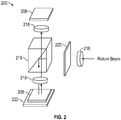
- FIG. 2 shows a portion 200 of another illustrative TOF depth imaging system. Only the image sensor 208, the electroabsorption modulator 206, some optics 218 (prism, lens), and optical filter 220 are shown. The other components of the TOF depth imaging system are similar to that of FIG. 1 .
- the electroabsorption modulator 206 of FIG. 2 is configured as a double-pass electroabsorption modulator (see FIGs. 10-12 ) wherein the reflected light from the object 102 (with reference to FIG.
- FIG. 1 passes through the electroabsorption modulator 206 twice before being directed to the image sensor 208.
- the electroabsorption modulator 206 may include a mirror or reflector 222.
- FIG. 3 shows a portion 300 of another illustrative TOF depth imaging system. Only the image sensor 308, the electroabsorption modulator 306 including the mirror/reflector 322, some optics 318, and the optical filter 320 are shown. The other components of the TOF depth imaging system are similar to that of FIG. 1 .
- the electroabsorption modulator 306 of FIG. 3 is also configured as a double-pass electroabsorption modulator (see FIGs. 10-12 ) wherein the reflected light from the object 102 passes through the electroabsorption modulator 306 twice before being directed to the image sensor 308.
- the TOF depth imaging systems of FIGs. 1-3 may be implemented in a single device which may be referred to as a TOF depth imaging camera, or may be implemented in a plurality of separate, but coupled devices.
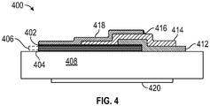
- FIG. 4 shows an illustrative electroabsorption modulator 400 which may be used, e.g., in the TOF depth imaging system 100 of FIG. 1 .
- the electroabsorption modulator 400 comprises a top doped layer of semiconductor 402, a bottom doped layer of semiconductor 404 having opposite polarity to the top doped layer and an active layer 406 between the top and bottom doped layers 402, 404.
- the active layer 406 is configured as a superlattice structure comprising multiple sublayers of semiconductor configured to provide alternating quantum wells and barriers. As such, the phrase "multi-quantum well (MQW)" may be used with reference to the active layer 406.
- MQW multi-quantum well
- the active layer 406 is configured to absorb light, e.g., via an interband-transition between a conduction subband and a valence subband of the active layer 406. However, as shown in FIG. 5 , the absorption edge of the active layer 406 may be red-shifted from its initial position in the absence of an external electric field (i.e., zero applied voltage) by the application of an external electric field (i.e., via an applied voltage V 0 ) according to the bulk or quantum-confined stark effect.
- an external electric field i.e., zero applied voltage
- the absorption edge of the active layer 406 may also be red-shifted from its initial position in the presence of a small external electric field (i.e., an applied low voltage, e.g., 8 V) by the application of a larger external electric field (i.e., via the applied voltage V 0 ).
- ⁇ 0 is the operating wavelength of the electroabsorption modulator 400.
- the operating wavelength ⁇ 0 is the wavelength at which the transmission at zero voltage (or low voltage) is relatively high, e.g., maximized, and the transmission at the higher voltage V 0 is relatively low, e.g., minimized.
- a narrow band optical filter 120 may be placed in series with the electroabsorption modulator 400. As shown in FIG. 6 , the narrow band optical filter 120 may be configured to maximize the transmission of light having wavelength ⁇ 0 while blocking other wavelengths.
- FIG. 7 shows the optical transmission of light having wavelength ⁇ 0 of the pair of the electroabsorption modulator 400 and the narrow band optical filter 120 as a function of voltage applied to the electroabsorption modulator 400.
- an oscillating voltage signal of magnitude V 0 to the electroabsorption modulator 400 will result in the variable transmission of light through the electroabsorption modulator 400, e.g., the modulation of reflected light received by the electroabsorption modulator 400 from the object 102 in the TOF depth imaging system 100 of FIG. 1 .
- the frequency of the oscillating voltage signal may be the modulation frequency f as described above.
- the composition of the semiconductor sublayers of the active layer 406, the thicknesses of the sublayers and the number of sublayers may be selected so that the operating wavelength ⁇ 0 of the electroabsorption modulator 400 substantially matches the selected wavelength ⁇ of the amplitude modulated light in the disclosed TOF depth imaging systems as described above (which may be light having a wavelength in the short-wave-infrared region, the near-infrared region or the visible region of the electromagnetic spectrum).
- the composition, thicknesses and number of the semiconductor sublayers may also be selected to maximize the difference in transmission at zero voltage (or low voltage) and transmission at voltage V 0 at the operating wavelength of the electroabsorption modulator 400.
- Quantum well(s) i.e., one or more or all of the active layer 406 may be configured to exhibit delocalized electron-hole behavior.
- z is the direction normal to the plane of the quantum well
- ⁇ e and ⁇ h are the electron and hole wavefunctions of the main subbands involved in the absorption of light of a particular wavelength (e.g., the selected wavelength ⁇ of the amplitude modulated light), respectively
- ⁇ e ⁇ and ⁇ h ⁇ are their complex conjugates.
- FIG. 8 illustrates the electron and hole wavefunctions for the main conduction and valence subbands involved in light absorption in a quantum well configured to exhibit delocalized electron-hole behavior as a function of position z along the direction normal to the plane of the quantum well. The expectation position values for the electron and the hole are also shown.
- the amount of electron-hole delocalization in the quantum well(s) may vary, depending upon the desired electroabsorption modulator. The amount of electron-hole delocalization may be selected to prevent or limit a decrease in the modulation depth and modulator efficiency.
- quantum well(s) of the active layer 406 are configured such that the expectation value of the electron position and the expectation value of the hole position differ by at least 1 atomic layer thickness. In some embodiments, quantum well(s) of the active layer 406 are configured such that the difference in the expectation value of the electron position and the expectation value of the hole position is in the range of from 1 atomic layer thickness to the thickness of the quantum well(s).
- quantum well(s) of the active layer 406 are configured such that the difference in the expectation value of the electron position and the expectation value of the hole position is in the range of from 0.3 nm to 20 nm, or in the range of from 0.3 nm to 10 nm, or in the range of from 0.3 nm to 5 nm.
- the quantum wells may be considered to be configured to exhibit delocalized electron-hole behavior.
- the result of delocalized electron-hole behavior in a quantum well is weaker optical absorption of the quantum well due to the reduced overlap integral.
- the use of such weakly absorbing quantum wells is contrary to the approach embodied by conventional TOF depth imaging systems employing conventional electro-optic shutters in which the overall thickness of the active layer is minimized to reduce the magnitude of the electric field needed to achieve the desired transmission variation and thus, to reduce power consumption.
- Such a conventional approach demands the use of more strongly absorbing quantum wells to accommodate for thinner active layers.
- the inventor has determined that use of quantum wells configured to exhibit delocalized electron-hole behavior, which increases the amount of absorption edge shift per voltage, may be a useful advantage, e.g., in TOF depth imaging systems.
- the number of sublayers of the quantum wells of the active layer 406, the composition of the quantum well sublayers and the thicknesses of the quantum well sublayers may be selected so that the quantum wells exhibit the delocalized electron-hole behavior described above.
- square quantum wells composed of a single layer of semiconductor may be configured to exhibit delocalized electron-hole behavior by the application of a delocalizing constant electric field (in addition to any oscillating electric field being applied to the electroabsorption modulator 400 to achieve modulation of reflected light in the TOF depth imaging system 100 of FIG.
- the delocalizing constant electric field is that which is sufficient to produce a delocalization of more than 1% of the FWHM of the square of the electron wavefunctions or the square of the hole wavefunctions of the square quantum well(s).
- the upper limit of the delocalization is when the overlap integral is less than 1% (i.e., 0.01), when the electron and hole wavefunctions are normalized (i.e., the integral of the wavefunction squared is unity).
- the delocalizing constant electric field is achieved by the application of a suitable delocalizing constant voltage, e.g., 0.5 to 15 V.
- the active layer 406 may comprise square quantum wells (or each of the quantum wells of the active layer may be square quantum wells).
- Square quantum wells are quantum wells formed from a single layer of semiconductor.
- square quantum wells composed of a single layer of semiconductor may be configured to exhibit delocalized electron-hole behavior by the application of a delocalizing constant electric field.
- the TOF depth imaging system 100 can comprise a voltage source configured to apply the delocalizing constant voltage to the electroabsorption modulator 400 to achieve the delocalizing constant electric field.
- the active layer 406 may comprise stepped quantum wells (or each of the quantum wells of the active layer may be stepped quantum wells).
- Stepped quantum wells are quantum wells formed from at least two quantum well sublayers of semiconductor, the at least two quantum well sublayers having different compositions and thus, different energy band gaps.
- the number of quantum well sublayers in the stepped quantum well may be two, three, four, etc.
- Stepped quantum wells exhibit delocalized electron-hole behavior due to the asymmetry in the energy band structure which leads to spatial separation of electron and hole wave functions.
- the particular band structure of the stepped quantum well(s) is not limited, provided the band structure is that which makes the electron wavefunction center of mass different from that of the hole (as described above).
- the active layer 406 comprises quantum wells having a type-II heterojunction (or each of the quantum wells of the active layer 406 are quantum wells having a type-II heterojunction).
- the composition, thickness and number of sublayers in the active layer 406 may be selected to achieve a desired effect on the transmission and absorption properties as well as a desired effect on the quantum well electron-hole wavefunctions of the electroabsorption modulator 400.
- the semiconductors used for the sublayers may be group III/V alloys (e.g., binary, ternary, quaternary alloys). Group III/V alloys are useful for electroabsorption modulators to be used with light having a wavelength in the near-infrared region of the electromagnetic spectrum (e.g., about 850 nm).
- the semiconductors used for the sublayers may be those in a GaAs-based system, e.g., any of the InGaAsP, GaInAsP, AlGaInP and AlGaAsP lattice matched systems.
- Strain-compensated active layers in which each of the sublayers are not lattice matched, but the overall strain is balanced to minimize or eliminate defects due to lattice mismatch may be used, e.g., a GaAs 1-x Sb x /Ga y In 1-y As z P 1-z system.
- the thicknesses of the sublayers of the active layer 406 may be less than about 100 nm, less than about 50 nm, less than about 20 nm, or less than about 10 nm. This includes thicknesses in the range of from about 1 nm to about 100 nm, from about 1 nm to about 50 nm, from about 1 nm to about 20 nm or from about 1 nm to about 10 nm.
- the selected overall thickness will be substantially thicker than a value which would be selected if the quantum wells of the active layer 406 were not configured to exhibit delocalized electron-hole behavior.
- the selected overall thickness may be greater than a value at which value the depth resolution coefficient K would be minimized if the quantum wells of the active layer 406 were not configured to exhibit delocalized electron-hole behavior.
- the overall thickness L of the active layer is 1 ⁇ m or greater, 2 ⁇ m or greater, 3 ⁇ m or greater, 5 ⁇ m or greater, or 7 ⁇ m or greater.
- These overall thicknesses L are substantially thicker than the active layers of conventional electro-optic shutters.
- the term "active layer" refers to the light-absorbing layers of the electroabsorption modulators.
- the thickness of the active layer of a conventional electro-optic shutter does not include the thickness of any layers forming an optical cavity associated with the active layer of such conventional electro-optic shutters since such an optical cavity does not substantially absorb light.
- An illustrative active layer may be composed of GaAs quantum wells and Al x Ga 1-x As barriers, e.g., 7 nm thick GaAs quantum wells and 6 nm thick Al 0.3 Ga 0.7 As barriers.
- Another illustrative active layer may be composed of two-step GaAs/Al x Ga 1-x As stepped quantum wells and Al x Ga 1-x As barriers, e.g., 9 nm thick Al 0.1 Ga 0.9 As first quantum well sublayers, 2 nm thick GaAs second quantum well sublayers and 6 nm thick Al 0.3 Ga 0.7 As barriers.
- Active layers for electroabsorption modulators to be used with light having a wavelength in the short-wave infrared region (SWIR) of the electromagnetic spectrum may include layers of InP/InAlAs/InGaAs/InGaAsP/InGaAsSb placed in such sequence to produce a large electron-hole wavefunction delocalization.
- These compositions could be either lattice matched to InP substrates, or strain compensated.
- An example includes In 0.54 Ga 0.46 As (5 nm)/In 0.59 Ga 0.41 As 0.89 P 0.11 (3 nm)/In 0.7 Ga 0.3 As 0.64 P 0.36 (3.5 nm)/In 0.53 Ga 0.47 As (9 nm), all undoped.
- This multilayer sequence may be repeated many times to make a thick "active region" (i.e., active layer).
- the active region may then be surrounded by an n-type InP and a p-type InP (or a p-type lattice matched InAlAs) and finally a heavily doped InGaAs contact layer at the top to form the electroabsorption modulator.
- Another example includes In 053 Al 0.47 As (10 nm)/In 0.35 Ga 0.65 As 0.77 P 0.23 (18 nm)/ In 053 Al 0.47 As (1 nm)/In 0.53 Ga 0.47 As (3 nm)/ InP (10 nm), all undoped.
- this multilayer sequence may be repeated many times and sandwiched between similar layers to form the electroabsorption modulator.
- Active layers for electroabsorption modulators to be used for light having a wavelength in the mid-wave and long-wave infrared (MWIR & LWIR) regions of the electromagnetic spectrum may include layers of semiconductor material with narrow bandgap, such as InGaAsSb/InGaSb lattice matched to a GaSb substrate, or strain balanced to a GaSb substrate with cutoff wavelengths from 2 ⁇ m to 30 ⁇ m.
- active layers may be made of different periods of type-II superlattices. For example, one period could be made of five bi-layers of GaSb (4 nm)/InAs (5.4 nm) and then five bi-layers of GaSb (3nm)/InAs (4.8nm).
- Electroabsorption modulators based on free-carrier absorption could also be made in the MWIR/LWIR spectral regions.
- ITO indium tin oxide
- a thin dielectric e.g. Al 2 O 3
- Active layers for electroabsorption modulators to be used for light having a wavelength in the ultraviolet (UV) region of the electromagnetic spectrum may include layers of wide bandgap semiconductors such as InGaN/GaN/AlGaInN.
- the piezoelectric effect combined with the strain produced by lattice mismatch could be used to produce a built-in electric field - and hence electron-hole wavefunction separation as explained herein.
- the relative amounts of the alloys may vary, e.g., AlGaAs is understood to encompass layers wherein the relative amounts of Al and Ga vary, i.e., Al x Ga 1-x As.
- the electroabsorption modulator 400 comprises a top doped layer of semiconductor 402 (e.g., p-type Al 0.3 Ga 0.7 As) and a bottom doped layer of semiconductor 404 having opposite polarity to the top doped layer (e.g., n-type Al 0.3 Ga 0.7 As) which sandwich the active layer 406.
- the active layer 406 may be in direct contact with the top and bottom doped layers 402, 404. Each of these layers may be disposed over a doped substrate 408.
- the bottom doped layer of semiconductor 404 has the same polarity as the substrate 408.
- the doping profile and doping level of the top and bottom doped layers 402, 404 may be selected so as not to produce a large free-carrier absorption, while the applied electric field is also maintained at a low value under the external bias.
- the top and bottom doped layers 402, 404 may have a thickness in the range of from about 100 nm to about 500 nm and a doping level of about 5 x 10 17 cm -3 .
- FIG. 4 also shows that the electroabsorption modulator 400 may include several other material layers.
- the electroabsorption modulator 400 may include a thin (e.g., about 10 nm to about 100 nm) contact layer of very highly doped (e.g., 10 19 cm -3 ) small bandgap material (e.g., GaAs or GaInAs) disposed over the top doped layer 402.
- Each of the semiconductor layers in the electroabsorption modulator 400 may be grown using a variety of epitaxial growth techniques, e.g., molecular beam epitaxy (MBE) and metalorganic vapor phase epitaxy (MOVPE). After the epitaxial layers have been grown, the resulting multilayer semiconductor structures may be processed using microfabrication techniques to deposit other material layers as described below.
- MBE molecular beam epitaxy
- MOVPE metalorganic vapor phase epitaxy
- a mesa may be defined and etched either by wet chemical etching or dry etching techniques, e.g., reactive ion etching (RIE).
- the multilayer semiconductor structure may be covered by a layer of an insulating material 412 (e.g., SiO 2 , Si 3 O 4 , or an insulating polymer, e.g., polyimide or benzocyclobutene).
- a window may be opened in the layer of insulating material 412 and a top contact layer 414 of a highly conductive material (e.g., metal) may be disposed over the top doped layer 402.
- the top contact layer 414 may be configured in a pattern which is sufficient to maximize the lateral voltage uniformity at the top contact layer 414 at high frequencies while minimizing the fill-factor (i.e., blocking light).
- the pattern may be a fractal pattern, including a branching fractal pattern.
- Such patterns may be optimized using finite-element-method (FEM) simulation tools to simulate the voltage, combined with an optimization approach, e.g., genetic algorithm.
- FEM finite-element-method
- a layer of a transparent conductive material 416 may be disposed over the top doped layer 402 in order to enhance the lateral conductivity before or after the top contact layer 402 is formed.
- the electroabsorption modulator 400 may include a bottom contact layer (not shown) electrically coupled to the bottom doped layer 404. This may be accomplished by accessing the bottom doped layer 404 from the top or from the bottom by making the bottom contact layer on the back of the substrate 408.
- the back contact layer is desirably configured so as to minimize light blocking.
- the electroabsorption modulator 400 may include a top antireflective coating 418 disposed over the top doped layer 402 and a bottom antireflective coating 420 disposed under the substrate 408 to minimize or prevent reflection due to refractive index change.
- the top and bottom antireflective coatings 418, 420 may be configured to minimize or prevent reflection over a wide range of incidence angles, e.g., a moth-eye configuration.
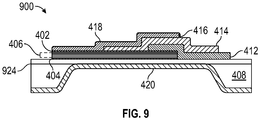
- FIG. 9 shows a variation on the embodiment of the electroabsorption modulator 400 of FIG. 4 , a variation which may be advantageous when using substrates which are not sufficiently transparent to the selected wavelength ⁇ of the amplitude modulated light.
- the electroabsorption modulator 900 of FIG. 9 includes each of the material layers as shown in FIG. 4 . However, the electroabsorption modulator 900 of FIG. 9 also includes an etch-stop layer 924 between the bottom doped layer 404 and the substrate 408. In addition, the substrate 408 has been sufficiently etched to minimize the absorption of light by the substrate 408.
- a window may be defined on the substrate 408 using a masking material (e.g., photoresist, dielectric, polymer, etc.) to protect the area not to be etched. Then, a selective chemical etch may be used with a sufficiently high etch rate for the substrate 408 but a sufficiently low etch rate for the etch-stop layer 924.
- a masking material e.g., photoresist, dielectric, polymer, etc.
- the electroabsorption modulators 400, 900 of FIGs. 4 and 9 are configured as single-pass electroabsorption modulators.
- single-pass it is meant that light received by each electroabsorption modulator passes through the respective active layer only once.
- Such a configuration is distinguished from conventional electro-optic shutters which include an optical cavity, e.g., by using a pair of distributed Bragg reflectors sandwiching the active layer.
- conventional electro-optic shutters light received by the electro-optic shutter passes through the active layer many multiple times.
- the electroabsorption modulators of FIGs. 4 and 9 do not comprise an optical cavity. That is, they are "cavity-less” or "cavity-free.”
- FIG. 10 shows another illustrative embodiment of an electroabsorption modulator 1000.
- This electroabsorption modulator 1000 is a double-pass electroabsorption modulator.
- double-pass it is meant that light received by the electroabsorption modulator 1000 passes through the active layer 1006 only twice.
- double-pass electroabsorption modulators also do not comprise an optical cavity and are also distinguished from conventional electro-optic shutters.
- the electroabsorption modulator 1000 of FIG. 10 comprises a top doped layer of semiconductor 1002, a bottom doped layer of semiconductor 1004 having opposite polarity to the top doped layer 1002 and the active layer 1006 between the top and bottom doped layers 1002, 1004.
- the electroabsorption modulator 1000 also includes a top contact layer 1026 of a highly conductive and reflective material (e.g., gold) disposed over the top doped layer 1002 and an antireflective coating 1020 disposed under the substrate 1008.
- An adhesion layer e.g., a 5 nm to 20 nm thick layer of Ti, Ni, or Cr
- the electroabsorption modulator 1000 may include other material layers as described above with respect to FIG. 4 .
- FIG. 11 shows another illustrative embodiment of a double-pass electroabsorption modulator.
- the electroabsorption modulator 1100 is a variation on the embodiment of the double-pass electroabsorption modulator of FIG. 10 , a variation which may be advantageous when using substrates which are not sufficiently transparent to the selected wavelength ⁇ of the amplitude modulated light.
- the electroabsorption modulator 1100 of FIG. 11 includes each of the material layers as shown in FIG. 10 . However, the electroabsorption modulator 1100 of FIG. 11 also includes an etch-stop layer 1124 between the bottom doped layer 1004 and the substrate 1008. In addition, the substrate 1008 has been sufficiently etched to minimize the absorption of light by the substrate 1008.
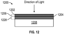
- FIG. 12 shows another illustrative embodiment of a double-pass electroabsorption modulator.
- the electroabsorption modulator 1200 of FIG. 12 comprises a top doped layer of semiconductor 1202, a bottom doped layer of semiconductor 1204 having opposite polarity to the top doped layer 1202 and an active layer 1206 between the top and bottom doped layers 1202, 1204. Each of these layers is disposed over a doped substrate 1208.
- the top and bottom doped layers 1202, 1204 and the active layer 1206 may be configured as described above with respect to FIG. 4 .
- the electroabsorption modulator 1200 also includes a single distributed Bragg reflector 1228 disposed under the active layer 1206, e.g., between the bottom doped layer 1204 and the substrate 1208.
- the electroabsorption modulator 1200 is distinguished from conventional electro-optic shutters as described above which include a pair of distributed Bragg reflectors to provide an optical cavity.
- the electroabsorption modulator 1200 may include other material layers as described above with respect to FIG. 4 .
- the thicknesses of the material layers of the disclosed electroabsorption modulators and the doping levels of the material layers may be selected such that the electroabsorption modulator exhibits a high breakdown voltage.
- the disclosed electroabsorption modulator may be characterized by its overall area relative to the overall area of the image sensor in any of the disclosed TOF depth imaging systems described above.
- ratio of the area of the electroabsorption modulator to the area of the image sensor is less than 1.
- the ratio of the area of the electroabsorption modulator to the area of the image sensor may be as low as ⁇ /(2 *n* X) ⁇ 2 wherein selected wavelength ⁇ is the selected wavelength of the amplitude modulated light, n is the optical refractive index of the semiconductor(s) of the electroabsorption modulator (e.g., n is about 3) and X is the pixel pitch of the image sensor.
- the disclosed electroabsorption modulator may be characterized by a number of other performance characteristics including, but not limited to, power consumption per area, voltage, field of view, modulation frequency, contrast, extinction ratio, single-pass transmission and single-pass absorption.
- an electroabsorption modulator configured to receive and to modulate reflected light from an object with the modulation frequency f comprises a top doped layer of semiconductor, a bottom doped layer of semiconductor having opposite polarity to the top doped layer, and an active layer between the top and bottom doped layers, the active layer configured as a superlattice structure comprising multiple sublayers of semiconductor configured to provide alternating quantum wells and barriers, the active layer comprising quantum wells configured to exhibit delocalized electron-hole behavior.
- An optoelectronic device is also provided, which in embodiments, comprises such an electroabsorption modulator.
- a method of modulating light is also provided, which in embodiments, comprises illuminating such an electroabsorption modulator with light and applying an oscillating voltage signal to the electroabsorption modulator.
- the disclosed electroabsorption modulators may be used in imaging systems for modulating photodiodes, retro-reflectors, and other large area optoelectronic devices.
- the disclosed electroabsorption modulators are configured as surface normal modulators which modulate the amplitude of a light beam and are distinguished from modulators which modulate the phase of a light beam.
- surface normal it is meant that the light to be modulated travels almost perpendicularly to the plane of the modulator. Similarly, light transmitted through the modulator travels almost perpendicularly to the plane of the modulator.
- the substrate of the electroabsorption modulators may be composed of a material which is sufficiently transparent to the selected wavelength ⁇ of the amplitude modulated light or which has been sufficiently etched to minimize the absorption of light by the substrate.
- the present disclosure is based, at least in part, upon the inventor's determination that the approach embodied in conventional TOF imaging systems employing electro-optic shutters (i.e., the use of thin active layers and optical cavities in such electro-optic shutters) in order to maximize depth resolution for a given power consumption is flawed. Below, this conventional approach is explained and distinguished from the approach embodied in the disclosed TOF imaging systems.
- T exp - ⁇ L
- L Another issue with large L relates to the uniformity of the electric field within an active layer comprising a series of quantum wells.
- the active layer of the modulator is sandwiched between a p-doped and an n-doped layer to form a p-i-n structure.
- the electric field can be localized in one side and can result in a non-uniform electric field.
- the presence of the optical cavity leads to a narrow spectral response of the electroabsorption modulator.
- the amount of enhancement is almost proportional to the cavity quality factor Q, while the optical bandwidth is inversely related to Q .
- the optical cavity also leads to an important limitation in TOF depth imaging systems, i.e., the resulted dispersion of the optical cavity is such that the transmission will be a function of the incident angle at the operating wavelength ⁇ 0 .
- the inventor's numerical calculation shows that an angular deviation of ⁇ ⁇ 10° leads to an increase in reflectivity from zero to about half of its maximum at the operating wavelength ⁇ 0 . (See FIGs. 13A-B .)
- the resulting numerical aperture N.A. ⁇ sin( ⁇ ) of such a modulator is about sin(10°) ⁇ 0.173, which results in a minimum effective pixel size of about 2 ⁇ 0 / ⁇ sin( ⁇ ), or about 3 ⁇ m at the operating wavelength of ⁇ 0 ⁇ 850 nm.
- Other system restrictions will only make the effective pixel size worse.
- the electroabsorption modulators disclosed herein do not require an optical cavity.
- the numerical apertures of the disclosed electroabsorption modulators may be very large (e.g., at least about 0.5, at least about 0.8, at least about 0.9, about 1).
- a numerical aperture of 0.8 leads to an effective pixel size of about 0.65 ⁇ m (about 4.6 times smaller than the effective pixel size of the conventional electro-optic shutter of Park.)
- the area of the disclosed electroabsorption modulators may be ( ⁇ 4.6) 2 or ⁇ 21 times smaller than the area of the conventional electro-optic shutter of Park.
- the power consumption of the disclosed electroabsorption modulators may be significantly reduced as compared to the conventional electro-optic shutter of Park (see Equations 3-5). Similarly, for a given area, this means that the number of resolved lateral points (pixels) may be about 21 times larger for the disclosed electroabsorption modulators.
- the large numerical apertures possible for the disclosed electroabsorption modulators may be used in different ways for different advantages in a TOF depth imaging system.
- the description above assumes that the electroabsorption modulator is located right above the image sensor. If, however, the electroabsorption modulator is moved to the Fourier location (e.g. by using a lens), then the larger numerical aperture means that the effective pixel size is not changed, but the area of the field of view is increased by the same factor. This will lead to the same enhancement in the number of pixels as shown in the calculations above.
- removing the optical cavity can lead to lower power consumption per unit area and good performance can be achieved by using a relatively thick active layer comprising quantum wells configured to exhibit delocalized electron-hole behavior.
- a relatively thick active layer comprising quantum wells configured to exhibit delocalized electron-hole behavior.
- conventional electro-optic shutters e.g., the electro-optic shutter of Park
- the active layer does not comprise quantum wells configured to exhibit delocalized electron-hole behavior.
- the active layer of the electro-optic shutter has a thickness L of about 0.5 ⁇ m.
- the transmission T of the electro-optic shutter can be changed from about 65% to about 15%.
- the value of K is unity for an ideal electroabsorption modulator (i.e. one having a T max of 100% and a MD of 100%).
- the value of K will increase above unity.
- K is about 1.46, which means that the depth resolution is about 1.46 times the depth resolution of a system with an ideal modulator.
- the inventor has determined that this conventionally accepted conclusion is flawed.
- electroabsorption modulators which comprise relatively thick active layers comprising quantum wells configured to exhibit delocalized electron-hole behavior, but which do not comprise an optical cavity can achieve improved performance as compared to conventional electro-optic shutters as well as provide lower power consumption per unit area.
- Depth resolution of an electroabsorption modulator comprising an active layer comprising quantum wells configured to exhibit delocalized electron-hole behavior
- Simulations were performed for an electroabsorption modulator comprising an active layer having a thickness L of about 4 ⁇ m and an operating wavelength ⁇ 0 of about 860 nm.
- the quantum wells of the active layer were square quantum wells which were configured to exhibit delocalized electron-hole behavior by the application of a delocalizing constant electric field (i.e., by applying a delocalizing constant voltage to the electroabsorption modulator).
- a delocalized constant voltage was applied to the electroabsorption modulator and then an additional oscillating voltage signal was applied.
- the delocalizing constant electric field has a frequency of nearly zero and thus, requires negligible power as predicted by Equations 3-5.
- a delocalizing constant electric field E 0 of 9.7 V/ ⁇ m was used and a modulating electric field E m of 3 V/ ⁇ m was used to change the electric field from 9.7 V/ ⁇ m to 12.7 V/ ⁇ m for the high and low transmission states of the electroabsorption modulator.
- the modulating voltage makes the absorption coefficient of the electroabsorption modulator change from about 700 cm -1 to about 4500 cm -1 .
- T max is about 0.755
- MD is about 0.79
- K is about 1.45, which is similar to the modified electro-optic shutter described above and better than the electro-optic shutter of Park.
- the change in electric field used to achieve these results is only about 3 V/ ⁇ m, i.e., about 3.1 times smaller than before.
- the total effect is that the power consumption is 8/9.6 or 83% of the cavity design, while the depth resolution is about 12% better.
- FIG. 14 illustrates the exact relation between the depth resolution coefficient K, the delocalizing constant electric field E 0 , and the thickness L of the active layer.
- the results were obtained for an electroabsorption modulator having an area A of 6 mm x 7 mm.
- the power consumption was set at 14 Watts for a modulating frequency f of 10 MHz.
- the depth resolution coefficient K is minimized at L ⁇ 1.2 ⁇ m.
- this minimum value is about K ⁇ 3, which means three times worse than the performance of an ideal electroabsorption modulator.
- the area of the disclosed electroabsorption modulators may be ( ⁇ 4.6) 2 or ⁇ 21 times smaller than the area of conventional electro-optic shutters, resulting in even further reduced power consumption.
- the present example is based on an electroabsorption modulator comprising an active layer based on square quantum wells.
- the results may be generalized for any quantum well design.
- quantum wells e.g., stepped quantum wells
- quantum wells which are configured to exhibit delocalized electron-hole behavior by adjusting the number of sublayers of the quantum wells, the compositions of the quantum well sublayers and the thicknesses of the quantum well sublayers, may be particularly advantageous. This is because such quantum wells may replace the need for the application of a large delocalizing constant voltage to delocalize the wavefunctions.
- the results described above may be achieved starting at a much lower delocalizing constant field than 9.7 V/ ⁇ m, e.g., even near zero bias.
- the equivalent "built-in" delocalizing constant electric field E 0 for such quantum wells is approximately equal to an opposite electric field that leads to elimination of electron-hole delocalization, or when ⁇ z e ⁇ z h ⁇ .
- the principle of operation of the electroabsorption modulators is based on the so-called quantum confined stark effect (QCSE).
- QCSE quantum confined stark effect
- An electroabsorption (EA) modulator is a device made of a quantum well (QW), or a series of QW, embedded within a stack of doped semiconductors such that the electric field within the QW region can be changed by exerting an external voltage across the device.
- QW quantum well
- QW quantum well
- the absorption edge of the device is the wavelength below which the absorption of light increases exponentially (due to increasingly higher energy of photons versus the effective bandgap of the QW).
- the principle of QCSE shows that once an electric field is applied to the QW region the absorption edge will shift to the longer wavelengths.
- the operation of the EA modulator is based on the absorption edge shift: a beam of light with wavelength longer than absorption edge can pass through the modulator with little attenuation. However, when an electric field is applied, the absorption edge shifts to longer wavelengths beyond the wavelength of light. This leads to a significant increase of light absorption by the QW leading to a significant reduction of light transmission (high attenuation). Therefore, the transmission of light can be modulated with an external voltage applied to the device.
- the wavelength of the excitonic peak of a QW shifts in quadratic relation versus the applied electric field (and hence, the applied voltage).
- this quadratic relation can be used to enhance the performance of surface-normal EA modulators, such as ones used for Time of Flight (ToF) 3D imaging described above.
- the absorption edge of the QW also shifts with quadratic (or even higher order) versus the applied electric field.
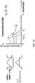
- the QCSE shift is a quadratic function of the electric field (approximately), which means that the shift per given change of electric field is higher at higher electric fields (Equation 6): ⁇ ⁇ ⁇ 0 + A E 2 ⁇ ⁇ ⁇ ⁇ E ⁇ 2 AE This concept is illustrated in FIG. 16 (left image), which also shows the rapid decrease of the peak absorption coefficient (right image) versus the applied external electric field.
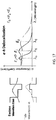
- FIG. 17 illustrates a QW potential designed to exhibit e-h delocalization behavior (left image). The result is a reduction of the optical absorption peak, but an increase in the change of peak absorption wavelength versus applied external field (i.e. ⁇ ⁇ ⁇ E ) (right image).
- Equation 7 shows that the shift of the peak absorption wavelength (and the absorption edge) is now a more sensitive function of the external field E.
- a consequence of the e-h delocalization is the reduction in the optical transfer matrix element, due to the reduced wavefunction overlap integral, which reduces the optical absorption coefficient (see FIG. 18 , right).
- the inventor has determined that despite this consequence, in ToF imaging, the performance of such a surface-normal EA modulator may surpass a conventional surface-normal EA modulator that does not comprise QWs configured to exhibit e-h delocalization behavior.
- the inventor has determined that the reduced absorption coefficient ⁇ can be compensated by increasing the thickness of the modulator, since the overall transmission is exp(- ⁇ . L ).
- E the voltage
- V E.L
- the thicker the modulator (bigger L ) the higher the voltage V.
- the power consumption for the modulator is proportional to CV 2
- V proportional to L
- C is inversely proportional to L
- the overall power consumption is proportional to L (power linearly increases with thicker modulator for a giver electric field).
- the transmission is an exponential function of L , and at some thickness the benefit will be optimum for a given power consumption. As shown in FIG.
- the e-h delocalization means that a larger L is now producing the optimum performance ( L optimum ⁇ 4 ⁇ m for the e-h delocalization).
- the electroabsorption modulators may be used in various applications requiring the modulation of light (e.g., light having a wavelength in the short-wave-infrared region, the near-infrared region or the visible region of the electromagnetic spectrum). Such applications involve illuminating any of the disclosed electroabsorption modulators with light and applying an oscillating voltage signal characterized by a desired frequency in order to modulate the transmission of the light through the electroabsorption modulator.
- TOF depth imaging Such an application involves illuminating an object with amplitude modulated light characterized by a wavelength ⁇ and a modulation frequency f to generate reflected light from the object, modulating the reflected light from the object using any of the disclosed electroabsorption modulators to generate modulated reflected light, and detecting the modulated reflected light from the electroabsorption modulator via an image sensor. Any of the disclosed TOF depth imaging systems may be used to carry out such an application.
- This example presents the results of the first 3D time of flight (ToF) camera operating in the short-wave infrared (SWIR) at 1550 nm. It includes a surface-normal cavity-less electroabsorption modulator with a backside mirror and an Er doped fiber laser amplifier (EDFA) at 150 MHz modulation frequency.
- EDFA Er doped fiber laser amplifier
- a field programmable gate array (FPGA) generates four quadrature phase shifts on the modulator's driver with respect to the EDFA. Therefore, a commercial SWIR camera turns into a 3D camera.
- a 4-mm objective lens maps the reflected light from an illuminated scene onto the backside of the modulator.
- the reflected light from backside is mapped onto the 320 by 256 pixels image sensor of the SWIR camera by the 50-mm camera lens.
- the results are presented below along with a discussion of design details and system performance.
- the capability of adding depth dimension to the SWIR camera greatly increases the versatility of SWIR applications.
- SWIR cameras have several advantages over devices that work in the visible or longer wave infrared bands.
- the SWIR band provides realistic night vision that is useful for navigation and is powerful for machine vision due to its ability to see through glasses and layers that are not captured by visible cameras.
- an unique time of flight system has been created that has the ability to take advantage of SWIR band optical properties.
- This example is a demonstration of the first indirect ToF 3D SWIR camera based on the 4-phase technique that is operating at 150 MHz modulation frequency.
- a modulated light illuminates a scene and the reflected light is captured by a ToF sensor. Since depth measurement is tied to the detection of phase accumulation of traveling light in the path of source-object-imager, higher time resolution can be achieved at higher modulation frequencies.
- a key innovation in this system is the use of the electroabsorption modulator described below as a global shutter to demodulate the reflected light from an object before being captured by an image sensor.
- Such a modulator can operate at GHz range frequencies providing unprecedented resolution performance.
- such a modulator is very good fit for near-infrared (NWIR) applications as this feature allows one to take advantage of off the shelf state-of-the-art CMOS image sensors.
- NWIR near-infrared
- a scene is illuminated with a modulated light and the reflected light from the objects in the scene is demodulated with four different phase shifts and captured by each individual pixel of the image sensor in a certain integration time to generate four quads of Q 0 , Q 90 , Q 180 and Q 270 .
- B the noise from image sensor and background
- A the demodulated signal
- it the reflected power from scene, which is captured by each image sensor's pixel.
- the accuracy can be improved by the square root of the reflected power depth, whereas it can be directly improved by modulation frequency and modulation contrast. Therefore, considering power consumption, it is more beneficial to choose a better modulator that offers high modulation depth and modulation frequency than increasing illumination power.
- the demodulation process to unwrap the phase can be persuaded both optically and electronically.
- each pixel of the image sensor demodulates the captured signal.
- PMD photo-modulated device
- ToF cameras have been developed based on this method, all operating at 850 nm. Despite the fact that this approach is attractive due to its compatibility with CMOS processes, modulation frequency beyond 100 MHz is very challenging due to controlling the level of cross-talk with adjacent pixels.
- local electronic modulation puts strict limits on pixel size due to the complexity of the individual pixels. The highest frequency that has been reported in electronics-level modulation is 130 MHz.
- optics-level demodulation can reach GHz speeds and allows for decoupling the demodulation process from the image acquisition.
- a global optical shutter is placed between the scene and image sensor to demodulate the incoming signal and unwrap the phase.
- the conventional optics-level demodulation approach taken by Park has been described above (an electro-absorptive cavity based modulator at 850 nm as a global shutter and an RGB image sensor to capture demodulated quads).
- reaching speeds in the GHz range requires a significant reduction of the modulator size, regardless of modulation mechanism. Therefore, a working GHz system requires a modulator that is smaller than the image sensor.
- mapping the incoming image to the modulator requires high NA optics.
- High NA optics is associated with focal beams with high angles. This implies that the modulator has to maintain its performance for high angles of incidence. Lack of a wide angular acceptance leads to a limitation on the modulation frequency.
- an optical cavity increases the modulation depth by increasing optical path at the expense of severe limitation on the range of acceptance angles.
- a small angle of acceptance sets an upper limit on the NA of optics that can be used to couple the beam passing from the modulator to the image sensor.
- the approach of Park cannot shrink the size of the modulator in order to reach GHz speeds.
- optics-level modulators have stayed below 20 MHz modulation frequency due to the aforementioned limitations.
- the optical cavity increases the sensitivity of the modulator to the applied voltage as well as junction temperature, resulting in further complexity at a system level.
- conventional approaches have shifted back to using electronic-level modulation to realize the next generation 3D cameras.
- the approach taken in the present disclosure involves optics-level modulation; therefore, it does not have the limitations of electronics-level modulation.
- it is fundamentally much more sensitive to applied voltage compared to the modulator of Park due to special design of the disclosed modulator.
- the exceptional sensitivity allows the elimination of an optical cavity based structure.
- the cavity-less feature provides a modulator with very high angle of acceptance that is favorable for high NA optics. Therefore GHz speeds can be realized due to the reduction of constraints on the modulator's size.
- FIG. 19 illustrates the TOF depth imaging system 1900 used in this example.
- the experimental setup includes several electrical and optical components working together, including the light source 1904 (a laser diode operating at 1550 nm), the electroabsorption modulator 1906, and the SWIR camera 1908 (which includes a 50 mm camera lens and an image sensor). Additional details are further described below.
- the light source 1904 a laser diode operating at 1550 nm
- the electroabsorption modulator 1906 which includes a 50 mm camera lens and an image sensor. Additional details are further described below.
- the microscope is arranged based on infinite optics. After the modulated illumination signal is incident on a scene 1902, the reflected signal is collected through a lens tube 1903 to reduce noise from source outside of the scene 1902. The collected signal is split by a 50/50 beam splitter 1918, sending half of the received signal into a 50x microscope objective 1919. The objective 1919 focuses the received signal onto the modulator's 1906 surface.
- the backside of the modulator 1906 is coated with gold acting like a mirror as well as back electrical contact to drive the modulator 1906.
- the modulator 1906 is configured as a double-pass electroabsorption modulator as described above.
- the modulator 1906 is configured for use with SWIR light (e.g., 1550 nm light) as described above, including an active layer comprising quantum wells configured to exhibit delocalized electron-hole behavior.
- SWIR light e.g., 1550 nm light
- the collimated signal passes through the beam splitter 1918 and finally is mapped on the camera's 1908 pixels through the camera lens.
- a field of view (FOV) of 8 degree (horizontal) by 11 degree (vertical) is imposed by the 50 mm camera lens with f-number of 1.8.
- the image of modulator 1906 is mapped into the image sensor of the camera 1908 with a magnification of 12.5 (ratio of camera lens to objective lens: 50 mm/4 mm).
- the image sensor has 320 by 256 pixels of 30 micron pitch, producing an imaging area of 9.60 mm by 7.68 mm. Therefore, the modulator area has to be ⁇ 0.5 mm 2 (0.768 mm by 0.614 mm).
- the modulator 1906 used has a similar area with circular shape. With regard to high angle optics, the modulator 1906 exhibits excellent performance despite the fact that the objective 1919 has NA-0.42.
- a field programmable gate array (FPGA) was used to generate and control the modulation frequency signals used to drive the light source 1904 and the modulator 1906.
- the quadrature modulation signals were generated internally by a Spartan VI FPGA board from Xilinix.
- an IP core provided by Xilinix was used to generate a Digital Clock Manager (DCM).
- the DCM can take an input signal and generate 4 outputs each phase shifted by 0, 90, 180, 270 degrees respectively.
- the outputs of the DCM were fed into a 4 to 1 digital multiplexer (also programmed within the FPGA).
- a C++ program was used to read out frames from the camera 1908 and to synchronize the quad signal switching trigger from the computer.
- the algorithm used to capture the quads had two steps: In the quad acquisition stage, each quad is captured several times and averaged to improve its signal to noise ratio (SNR). In depth acquisition stage, four averaged quads are captured to produce depth information. Taking several depth images and average them, improves SNR further.
- SNR signal to noise ratio
- the output of the FPGA was fed to a voltage amplifier (TI THS3001CD). The output of the voltage amplifier was fed through a bias-tee to apply a -50 volt bias. Finally the modulation signal was sent to the modulator 1906 contact pad through a specialized RF probe. In addition to providing the modulation signal to the optical modulator 1906, the FPGA in the setup also provides the modulation signal to the light source 1904. The zero degree phase shifted clock signal was fed out from the FPGA to the light source 1904 (a 5 mw DFB 1550 nm laser diode). The output of the laser was fed through a single mode 1550 fiber to an erbium doped fiber amplifier (EDFA). The output of the EDFA was fed through a fiber to a stand where the signal was free to expand into free space and illuminate the scene 1902. To reduce the effect of speckle noise in the images a rotating diffuser 1905 was placed at the output of the fiber holder.
- a voltage amplifier TI THS3001CD
- the output of the voltage amplifier
- an alternative setup was built that replaces the SWIR camera 1908 of FIG. 19 with a collimator that collects light into a multi-mode fiber.
- the signal was directly provided by injecting a collimated beam from the output of a tunable laser source.
- the laser signal was reflected by the beam splitter 1918 into the modulator 1906.
- the modulated signal was recollected once again by the microscope objective 1919 and then coupled into the multi-mode fiber to be measured by a PIN photodiode.
- the signal from the PIN detector was amplified through a low noise amplifier (LNA, SR570) as it is a dc coupled amplifier, whereas in high frequency mode, a voltage amplifier (DUPVA-1-70).
- LNA low noise amplifier
- DUPVA-1-70 a voltage amplifier
- the signal was measured on a 2.5 GHz oscilloscope which was being triggered optically at the chosen zero degree phase shifted modulation signal (either 50 MHz, 100 MHz, or 150 MHz) by another laser diode being driven by the FPGA and measured by a PIN detector. This configuration allowed a reduction of cross talk between the modulation and the trigger signal while directly measuring the phase shift of the signal with respect to the base clock of the DCM.
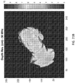
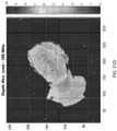
- FIGs. 20A-C show the depth measurements at 150 MHz (A), 100 MHz (B) and 50 MHz (C) of the statue after correction using the calibrating data.
- the images were derived by taking 6 images and averaging per quad measurement and 100 averages per depth measurement.
- the camera's 1908 integration time was set at 150 msec with high gain mode.
- FIG. 21A shows the SWIR image of the statute taken by the camera 1908.
- FIGs. 21B-D compare the depth resolution for different frequencies. To get depth resolution, the standard deviation of the whole measurement was calculated to get rms of depth data. Note that the values are assigned for a single depth measurement with 6 times averaging per quad. Taking 100 times averaging per depth measurement, the data in FIGs. 20A-C has rms 10 times smaller than what is shown in FIGs. 21B-D .
- FIG. 22 compares the modulation response of the system 1900 to the system of Park as a function of modulation frequency, demonstrating the superiority of the performance of the system 1900 and the approach to TOF depth imaging disclosed herein.
- the first SWIR 3D camera with 150 MHz modulation frequency has been demonstrated.
- the system can incorporate any commercial SWIR camera. This system has the benefit of allowing decoupling demodulation from image capturing, resulting in very high frequency modulation. This system may be used in many SWIR applications such as night vision and disturbed atmosphere.
Landscapes
- Physics & Mathematics (AREA)
- Engineering & Computer Science (AREA)
- General Physics & Mathematics (AREA)
- Nonlinear Science (AREA)
- Electromagnetism (AREA)
- Remote Sensing (AREA)
- Radar, Positioning & Navigation (AREA)
- Computer Networks & Wireless Communication (AREA)
- Optics & Photonics (AREA)
- Computer Vision & Pattern Recognition (AREA)
- Theoretical Computer Science (AREA)
- Optical Modulation, Optical Deflection, Nonlinear Optics, Optical Demodulation, Optical Logic Elements (AREA)
- Length Measuring Devices By Optical Means (AREA)
- Measurement Of Optical Distance (AREA)
- Photometry And Measurement Of Optical Pulse Characteristics (AREA)
Claims (16)
- TOF-Tiefenbildgebungssystem (100) zum Bereitstellen eines Tiefenbildes eines Objekts (102), wobei das System aufweist:eine Lichtquelle (104), die zum Beleuchten eines Objekts mit amplitudenmoduliertem Licht ausgebildet ist, das durch eine Wellenlänge λ und eine Modulationsfrequenz f gekennzeichnet ist;einen flächennormalen Elektroabsorptionsmodulator (106, 400), der zum Empfangen und zum Modulieren von reflektiertem Licht von dem Objekt mit der Modulationsfrequenz f ausgebildet ist, wobei der Elektroabsorptionsmodulator aufweist:eine obere dotierte Halbleiterschicht (402),eine untere dotierte Halbleiterschicht (404) mit entgegengesetzter Polarität zu der oberen dotierten Schicht, undeine Aktivschicht (406) zwischen der oberen und der unteren dotierten Schicht, wobei die Aktivschicht als eine Übergitterstruktur ausgebildet ist, die mehrere Halbleiterunterschichten aufweist, die zum Bereitstellen alternierender Quantentöpfe und Barrieren ausgebildet sind; undeinen Bildsensor (108), der zum Aufnehmen und zum Detektieren von moduliertem reflektiertem Licht von dem Elektroabsorptionsmodulator ausgebildet ist,dadurch gekennzeichnet, dass die Aktivschicht Quantentöpfe aufweist, die zum Aufzeigen von delokalisiertem Elektrononenlochverhalten ausgebildet sind, und dass der Elektroabsorptionsmodulator keinen optischen Resonator aufweist.
- TOF-Tiefenbildgebungssystem nach Anspruch 1, ferner mit einem ersten Treiber (110), der in elektrischer Kommunikation mit der Lichtquelle ist, einem zweiten Treiber (112), der in elektrischer Kommunikation mit dem Elektroabsorptionsmodulator ist, und einer Zeitsteuerung (114), die in elektrischer Kommunikation mit dem ersten und dem zweiten Treiber und dem Bildsensor (108) ist.
- TOF-Tiefenbildgebungssystem nach Anspruch 1, wobei die Aktivschicht (406) zum Absorbieren von Licht ausgebildet ist, das eine Wellenlänge im Nahinfrarotbereich des elektromagnetischen Spektrums aufweist, und wobei die mehreren Halbleiterunterschichten vorzugsweise aus Legierungen der Gruppe III/V bestehen.
- TOF-Tiefenbildgebungssystem nach Anspruch 1, wobei die Aktivschicht (406) zum Absorbieren von Licht ausgebildet ist, das eine Wellenlänge im kurzwelligen Infrarotbereich des elektromagnetischen Spektrums aufweist, und wobei die mehreren Halbleiterunterschichten vorzugsweise eine mehrschichtige Struktur aus InGaAs/InGaAsP/InGaAsP/InGaAs oder eine mehrschichtige Struktur aus InAlAs/InGaAsP/InAlAs/InGaAs/InP ausweisen.
- TOF-Tiefenbildgebungssystem nach Anspruch 1, wobei die Aktivschicht (406) zum Absorbieren von Licht ausgebildet ist, das eine Wellenlänge in dem mittelwelligen und langwelligen Infrarotbereich des elektromagnetischen Spektrums aufweist, und wobei die mehreren Halbleiterunterschichten eine mehrschichtige Struktur aus InGaAsSb/InGaSb-Gitter aufweisen, das mit einem GaSb-Substrat abgestimmt ist oder mit einen GaSb-Substrat belastungsausgeglichen ist.
- TOF-Tiefenbildgebungssystem nach Anspruch 1, wobei die Aktivschicht (406) zum Absorbieren von Licht ausgebildet ist, das eine Wellenlänge im ultravioletten Bereich des elektromagnetischen Spektrums aufweist, und wobei die mehreren Halbleiterunterschichten ferner eine mehrschichtige Struktur aus InGaN/GaN/AlGaInN aufweisen.
- TOF-Tiefenbildgebungssystem nach Anspruch 1, wobei die Aktivschicht (406) abgestufte Quantentöpfe aufweist, die aus mindestens zwei Quantentopfunterschichten eines Halbleiters bestehen, wobei die mindestens zwei Quantentopfunterschichten unterschiedliche Zusammensetzungen aufweisen, und wobei die abgestuften Quantentöpfe vorzugsweise zweistufig abgestufte Quantentöpfe sind, und wobei die zweistufig abgestuften Quantentöpfe besonders bevorzugt aus einer ersten GaAs-Quantentopfunterschicht und einer zweiten AlxGa1-xAs-Quantentopfunterschicht bestehen und die Barrieren aus AlxGa1-xAs-Barrieren bestehen.
- TOF-Tiefenbildgebungssystem nach Anspruch 1, wobei die Aktivschicht (406) Quantentöpfe mit einem Typ-II-Heteroübergang aufweist.
- TOF-Tiefenbildgebungssystem nach Anspruch 1, wobei die Aktivschicht (406) quadratische Quantentöpfe aufweist, die aus einer einzigen Halbleiterschicht bestehen, und wobei das TOF-Tiefenbildgebungssystem ferner eine Spannungsquelle aufweist, die zum Anlegen einer delokalisierten konstanten Spannung an den Elektroabsorptionsmodulator ausgebildet ist, um ein delokalisiertes konstantes elektrisches Feld zu erzielen.
- TOF-Tiefenbildgebungssystem nach Anspruch 1, wobei die Aktivschicht (406) eine Gesamtdicke L aufweist und die Gesamtdicke L einen Mindesttiefenauflösungskoeffizienten K des Elektroabsorptionsmodulators (106, 400) bereitstellt.
- TOF-Tiefenbildgebungssystem nach Anspruch 1, wobei die Aktivschicht (406) eine Gesamtdicke L aufweist und die Gesamtdicke L im Bereich von 1 µm bis 20 µm liegt.
- TOF-Tiefenbildgebungssystem nach Anspruch 1, wobei der Elektroabsorptionsmodulator (106, 400) als ein Einzelpass- oder ein Doppelpass-Elektroabsorptionsmodulator ausgebildet ist.
- TOF-Tiefenbildgebungssystem nach Anspruch 1, wobei der Elektroabsorptionsmodulator (106, 400) durch einen ersten Bereich gekennzeichnet ist und der Bildsensor durch einen zweiten Bereich gekennzeichnet ist, und wobei ferner das Verhältnis des ersten Bereichs zu dem zweiten Bereich weniger als 1 beträgt.
- TOF-Tiefenbildgebungssystem nach Anspruch 1, ferner mit einer kurzwelligen Infrarotkamera, wobei der Bildsensor (108) eine Komponente der kurzwelligen Infrarotkamera ist.
- TOF-Tiefenbildgebungssystem nach Anspruch 1, wobei die Modulationsfrequenz f mindestens 50 MHz beträgt.
- Verfahren zur TOF-Tiefenbildgebung mit folgenden Schritten:Beleuchten eines Objekts (102) mit amplitudenmoduliertem Licht, das durch eine Wellenlänge λ und eine Modulationsfrequenz f gekennzeichnet ist, um reflektiertes Licht von dem Objekt zu erzeugen;Modulieren des reflektierten Lichts von dem Objekt mittels eines flächennormalen Elektroabsorptionsmodulators (106, 400) zum Erzeugen von moduliertem reflektiertem Licht, wobei der Elektroabsorptionsmodulator aufweist:eine obere dotierte Halbleiterschicht (402),eine untere dotierte Halbleiterschicht (404) mit entgegengesetzter Polarität zu der oberen dotierten Schicht, undeiner Aktivschicht (406) zwischen der oberen und der unteren dotierten Schicht, wobei die Aktivschicht als eine Übergitterstruktur ausgebildet ist, die mehrere Halbleiterunterschichten aufweist, die zum Bereitstellen alternierender Quantentöpfe und Barrieren ausgebildet sind; undDetektieren des modulierten reflektierten Lichts von dem Elektroabsorptionsmodulator über einen Bildsensors (108),dadurch gekennzeichnet, dass die Aktivschicht Quantentöpfe aufweist, die zum Aufzeigen von delokalisiertem Elektrononenlochverhalten ausgebildet sind, und dass der Elektroabsorptionsmodulator keinen optischen Resonator aufweist.
Applications Claiming Priority (4)
| Application Number | Priority Date | Filing Date | Title |
|---|---|---|---|
| US201562126802P | 2015-03-02 | 2015-03-02 | |
| US201562131603P | 2015-03-11 | 2015-03-11 | |
| US201562235962P | 2015-10-01 | 2015-10-01 | |
| PCT/US2016/020256 WO2016140965A1 (en) | 2015-03-02 | 2016-03-01 | Electroabsorption modulator for depth imaging and other applications |
Publications (3)
| Publication Number | Publication Date |
|---|---|
| EP3265871A1 EP3265871A1 (de) | 2018-01-10 |
| EP3265871A4 EP3265871A4 (de) | 2018-10-10 |
| EP3265871B1 true EP3265871B1 (de) | 2020-11-25 |
Family
ID=56848487
Family Applications (1)
| Application Number | Title | Priority Date | Filing Date |
|---|---|---|---|
| EP16759354.0A Active EP3265871B1 (de) | 2015-03-02 | 2016-03-01 | Elektroabsorptionsmodulator für tiefenbildgebung und andere anwendungen |
Country Status (6)
| Country | Link |
|---|---|
| US (1) | US10254407B2 (de) |
| EP (1) | EP3265871B1 (de) |
| JP (1) | JP6734292B2 (de) |
| KR (1) | KR102546336B1 (de) |
| CN (1) | CN107430294B (de) |
| WO (1) | WO2016140965A1 (de) |
Families Citing this family (20)
| Publication number | Priority date | Publication date | Assignee | Title |
|---|---|---|---|---|
| US20170235162A1 (en) * | 2015-07-13 | 2017-08-17 | Purdue Research Foundation | Time-varying metasurface structure |
| US20170047708A1 (en) * | 2015-08-12 | 2017-02-16 | Finisar Corporation | Wavefunction deconfinement electro-absorption modulator |
| US10097281B1 (en) | 2015-11-18 | 2018-10-09 | Hypres, Inc. | System and method for cryogenic optoelectronic data link |
| US10514483B2 (en) | 2016-10-13 | 2019-12-24 | Massachusetts Institute Of Technology | Time-of-flight camera for imaging through optical cavity |
| JP6862751B2 (ja) * | 2016-10-14 | 2021-04-21 | 富士通株式会社 | 距離測定装置、距離測定方法及びプログラム |
| WO2019035876A1 (en) | 2017-08-15 | 2019-02-21 | Northwestern University | METHOD AND SYSTEM FOR READING AND STIMULATING NEURONS THROUGH TISSUE USING LIGHT |
| US10303921B1 (en) | 2018-02-26 | 2019-05-28 | Shenzhen GOODIX Technology Co., Ltd. | On-LCD screen optical fingerprint sensing based on optical imaging with lens-pinhole module and other optical designs |
| FR3084523B1 (fr) * | 2018-07-27 | 2020-12-25 | Soc Fr De Detecteurs Infrarouges Sofradir | Dispositif de detection electromagnetique |
| WO2020045770A1 (en) * | 2018-08-31 | 2020-03-05 | Samsung Electronics Co., Ltd. | Method and device for obtaining 3d images |
| WO2020055718A1 (en) * | 2018-09-12 | 2020-03-19 | Northwestern University | Methods and systems for efficient coupling of light from outside tissue to small volumes inside tissue |
| EP3874303A4 (de) * | 2018-11-02 | 2022-12-28 | Gary Sharp Innovations, Inc. | Kompakte polarisationsbasierte optische multipass-architekturen |
| CN113646906B (zh) * | 2019-04-09 | 2024-06-04 | 杜鹏 | 用于探测器的超晶格吸收体 |
| CN110275098B (zh) * | 2019-06-28 | 2021-07-09 | 杭州赫太克科技有限公司 | 紫外成像仪 |
| JP6857263B1 (ja) | 2020-01-17 | 2021-04-14 | 浜松ホトニクス株式会社 | 発光体、電子線検出器、及び走査型電子顕微鏡 |
| US12165342B2 (en) | 2020-05-21 | 2024-12-10 | Samsung Electronics Co., Ltd. | Method and apparatus for generating depth image |
| KR102733514B1 (ko) * | 2020-05-21 | 2024-11-25 | 삼성전자주식회사 | 깊이 영상을 생성하는 방법 및 장치 |
| CN113608371B (zh) * | 2021-07-13 | 2024-03-19 | 厦门大学 | 一种基于ii类断带能隙量子阱的红外电吸收调制器 |
| CN114481088B (zh) * | 2022-04-18 | 2022-07-01 | 苏州长光华芯光电技术股份有限公司 | 一种超晶格有源层及半导体发光结构的制作方法 |
| CN118565383B (zh) * | 2024-04-17 | 2025-01-24 | 武汉大学 | 双晶单色器平行度动态测量系统、方法 |
| CN119596279B (zh) * | 2024-12-17 | 2025-08-29 | 深圳市湾澳科技有限公司 | 一种谐振腔的光学成像系统及方法 |
Family Cites Families (53)
| Publication number | Priority date | Publication date | Assignee | Title |
|---|---|---|---|---|
| US5300788A (en) | 1991-01-18 | 1994-04-05 | Kopin Corporation | Light emitting diode bars and arrays and method of making same |
| US5345093A (en) | 1991-04-15 | 1994-09-06 | The United States Of America As Represented By The Secretary Of The Navy | Graded bandgap semiconductor device for real-time imaging |
| JP2550882B2 (ja) | 1993-09-28 | 1996-11-06 | 日本電気株式会社 | 赤外線撮像装置 |
| US5510627A (en) | 1994-06-29 | 1996-04-23 | The United States Of America As Represented By The Secretary Of The Navy | Infrared-to-visible converter |
| US5594750A (en) * | 1995-06-06 | 1997-01-14 | Hughes Aircraft Company | Selectively Si-doped InAs/A1AsSb short-period-superlattices as N-type cladding layers for mid-IR laser structures grown on InAs substrates |
| US6057909A (en) | 1995-06-22 | 2000-05-02 | 3Dv Systems Ltd. | Optical ranging camera |
| US5588015A (en) | 1995-08-22 | 1996-12-24 | University Of Houston | Light emitting devices based on interband transitions in type-II quantum well heterostructures |
| FR2741483B1 (fr) * | 1995-11-21 | 1998-01-02 | Thomson Csf | Dispositif optoelectronique a puits quantiques |
| US6028323A (en) | 1996-07-19 | 2000-02-22 | National Research Council Of Canada | Quantum well infared image conversion panel and associated methods |
| US5799026A (en) | 1996-11-01 | 1998-08-25 | The United States Of America As Represented By The Secretary Of The Navy | Interband quantum well cascade laser, with a blocking quantum well for improved quantum efficiency |
| JP3751423B2 (ja) * | 1997-10-01 | 2006-03-01 | 独立行政法人科学技術振興機構 | 半導体素子 |
| US7442953B2 (en) | 1999-06-14 | 2008-10-28 | Quantum Semiconductor Llc | Wavelength selective photonics device |
| US6875975B2 (en) | 1999-12-24 | 2005-04-05 | Bae Systems Information And Electronic Systems Integration Inc | Multi-color, multi-focal plane optical detector |
| US6674091B2 (en) | 2000-09-26 | 2004-01-06 | California Institute Of Technology | Multi-quantum-well detector for low-background applications |
| US7095542B2 (en) * | 2001-02-01 | 2006-08-22 | The Regents Of The University Of California | Electroabsorption modulator having a barrier inside a quantum well |
| US6500688B2 (en) | 2001-03-14 | 2002-12-31 | The United States Of America As Represented By The Secretary Of The Army | Interband cascade light emitting device and method of making same |
| US20060175550A1 (en) | 2002-06-06 | 2006-08-10 | Siddiqi Mahmud A | Use of a night-vision intensifier for direct visualization by eye of far-red and near-infared fluorescence through an optical microscope |
| JP2004140339A (ja) * | 2002-09-25 | 2004-05-13 | Univ Chiba | 窒化物系ヘテロ構造を有するデバイス及びその製造方法 |
| US6956232B2 (en) * | 2002-12-24 | 2005-10-18 | Triquint Technology Holding Co. | Electroabsorption modulator |
| US7064881B2 (en) | 2003-05-30 | 2006-06-20 | Sarnoff Corporation | InP-based phase modulators and methods for making and using same |
| US20050082520A1 (en) | 2003-10-06 | 2005-04-21 | Fathimulla Ayub M. | Monolithic two color quantum-well photodetector |
| FR2863774B1 (fr) | 2003-12-16 | 2006-03-03 | Thales Sa | Photodetecteur a concentration de champ proche |
| WO2006127028A2 (en) * | 2004-09-13 | 2006-11-30 | Northwestern University | Transparent conducting components and related electro-optic modulator devices |
| US7282777B1 (en) | 2004-09-27 | 2007-10-16 | California Institute Of Technology | Interband cascade detectors |
| US7259405B2 (en) | 2004-11-23 | 2007-08-21 | Au Optronics Corporation | Organic photoelectric device with improved electron transport efficiency |
| JP4663712B2 (ja) * | 2005-03-08 | 2011-04-06 | 日本電信電話株式会社 | 半導体光変調器 |
| US8748923B2 (en) | 2005-03-14 | 2014-06-10 | Philips Lumileds Lighting Company Llc | Wavelength-converted semiconductor light emitting device |
| US20070019274A1 (en) * | 2005-07-25 | 2007-01-25 | Scott Lerner | Double pass light modulator |
| WO2007038600A2 (en) | 2005-09-27 | 2007-04-05 | Northwestern University | A single-photon detector and applications of same |
| US7838869B2 (en) | 2005-10-21 | 2010-11-23 | Georgia State University Research Foundation, Inc. | Dual band photodetector |
| JP4639321B2 (ja) | 2005-11-14 | 2011-02-23 | コニカミノルタセンシング株式会社 | 生体情報測定装置 |
| US7843982B2 (en) * | 2005-12-15 | 2010-11-30 | Palo Alto Research Center Incorporated | High power semiconductor device to output light with low-absorbtive facet window |
| US7804640B1 (en) | 2007-05-24 | 2010-09-28 | University Of Central Florida Research Foundation, Inc. | Composite cavity for enhanced efficiency of up-conversion |
| US7963677B2 (en) | 2006-12-28 | 2011-06-21 | Seiko Epson Corporation | Light source device, having wavelength conversion and separation means, and projector |
| US7508858B2 (en) * | 2007-04-30 | 2009-03-24 | The Research Foundation Of State University Of New York | Detuned duo-cavity laser-modulator device and method with detuning selected to minimize change in reflectivity |
| US8039736B2 (en) | 2008-08-18 | 2011-10-18 | Andrew Clark | Photovoltaic up conversion and down conversion using rare earths |
| US8283633B2 (en) | 2007-11-30 | 2012-10-09 | Halliburton Energy Services, Inc. | Tuning D* with modified thermal detectors |
| JP4533939B2 (ja) | 2008-04-10 | 2010-09-01 | 三菱重工業株式会社 | 赤外線検出素子、赤外線検出装置及び赤外線検出素子の製造方法 |
| US8637875B2 (en) | 2008-07-11 | 2014-01-28 | The Regents Of The University Of California | Single photon IR detectors and their integration with silicon detectors |
| JP4459286B2 (ja) | 2008-08-08 | 2010-04-28 | 防衛省技術研究本部長 | 赤外線検知器 |
| JP2011035138A (ja) | 2009-07-31 | 2011-02-17 | Hamamatsu Photonics Kk | 半導体発光素子 |
| KR101608903B1 (ko) | 2009-11-16 | 2016-04-20 | 삼성전자주식회사 | 적외선 이미지 센서 |
| KR101675112B1 (ko) * | 2010-01-21 | 2016-11-22 | 삼성전자주식회사 | 거리 정보 추출 방법 및 상기 방법을 채용한 광학 장치 |
| WO2011127475A1 (en) | 2010-04-09 | 2011-10-13 | The Arizona Board Of Regents On Behalf Of The University Of Arizona | Organic photovoltaic devices comprising solution- processed substituted metal-phthalocyanines and exhibiting near-ir photo-sensitivity |
| WO2012021968A1 (en) | 2010-08-18 | 2012-02-23 | Dayan Ban | Organic/inorganic hybrid optical amplifier with wavelength conversion |
| US8829777B2 (en) | 2010-09-27 | 2014-09-09 | Osram Sylvania Inc. | Ceramic wavelength converter and LED light source containing same |
| US20140009905A1 (en) | 2010-12-16 | 2014-01-09 | Sharp Kabushiki Kaisha | Fluorescent substrate, display apparatus, and lighting apparatus |
| EP2477043A1 (de) * | 2011-01-12 | 2012-07-18 | Sony Corporation | 3D-Flugzeitkamera und Verfahren |
| WO2012109625A1 (en) * | 2011-02-10 | 2012-08-16 | Flir Systems, Inc. | Wavelength diverse scintillation reduction |
| KR101974576B1 (ko) * | 2012-04-12 | 2019-05-02 | 삼성전자주식회사 | 대면적을 갖는 투과형 광 이미지 변조기 및 그 제조 방법과 투과형 광 이미지 변조기를 포함하는 광학장치 |
| US9054247B2 (en) | 2012-06-25 | 2015-06-09 | Northwestern University | Single-photon nano-injection detectors |
| US9470952B2 (en) * | 2013-06-13 | 2016-10-18 | The Regents Of The University Of California | Sub-volt drive 100 GHz bandwidth electro-optic modulator |
| KR102038623B1 (ko) * | 2013-08-21 | 2019-10-30 | 삼성전자주식회사 | 광변조기 및 이를 포함한 3차원 영상 획득 장치 |
-
2016
- 2016-03-01 EP EP16759354.0A patent/EP3265871B1/de active Active
- 2016-03-01 KR KR1020177027354A patent/KR102546336B1/ko active Active
- 2016-03-01 WO PCT/US2016/020256 patent/WO2016140965A1/en not_active Ceased
- 2016-03-01 CN CN201680018769.3A patent/CN107430294B/zh active Active
- 2016-03-01 US US15/057,792 patent/US10254407B2/en active Active
- 2016-03-01 JP JP2017545947A patent/JP6734292B2/ja not_active Expired - Fee Related
Non-Patent Citations (1)
| Title |
|---|
| SCHWEDLER R ET AL: "INGAAS/INP MULTIPLE QUANTUM WELL MODULATORS IN EXPERIMENT AND THEORY", JOURNAL DE PHYSIQUE III, EDITIONS DE PHYSIQUE, PARIS, FR, vol. 4, no. 12, 1 December 1994 (1994-12-01), pages 2341 - 2359, XP000491696, ISSN: 1155-4320, DOI: 10.1051/JP3:1994281 * |
Also Published As
| Publication number | Publication date |
|---|---|
| KR102546336B1 (ko) | 2023-06-21 |
| US20160259059A1 (en) | 2016-09-08 |
| CN107430294B (zh) | 2020-12-29 |
| JP2018514749A (ja) | 2018-06-07 |
| EP3265871A4 (de) | 2018-10-10 |
| JP6734292B2 (ja) | 2020-08-05 |
| EP3265871A1 (de) | 2018-01-10 |
| KR20170120688A (ko) | 2017-10-31 |
| WO2016140965A1 (en) | 2016-09-09 |
| CN107430294A (zh) | 2017-12-01 |
| US10254407B2 (en) | 2019-04-09 |
Similar Documents
| Publication | Publication Date | Title |
|---|---|---|
| EP3265871B1 (de) | Elektroabsorptionsmodulator für tiefenbildgebung und andere anwendungen | |
| Chen et al. | Low dark current high gain InAs quantum dot avalanche photodiodes monolithically grown on Si | |
| WO2013184556A1 (en) | Ultra-thin optical coatings and devices and methods of using ultra-thin optical coatings | |
| EP2604574B1 (de) | Lichtdurchlässiger Bildmodulator mithilfe eines Multi-Fabry-Perot-Resonanzmodus und Multiabsorptionsmodus | |
| WO1995006272A1 (en) | Hybridized asymmetric fabry-perot quantum well light modulator | |
| CA2180960A1 (en) | Infrared image converter | |
| JP2014165412A (ja) | 短光パルス発生装置、テラヘルツ波発生装置、カメラ、イメージング装置、および計測装置 | |
| KR20130080641A (ko) | 다중 흡수 모드를 갖는 적층식 다이오드 구조의 투과형 이미지 변조기 | |
| Wen et al. | Broad-band spatial light modulation with dual epsilon-near-zero modes | |
| KR20150066154A (ko) | GaAs 기판에 격자 정합되는 다중 양자 우물 구조를 포함하는 광학 소자, 이를 포함하는 깊이 영상 획득 장치 및 3차원 영상 획득 장치 | |
| US20210124235A1 (en) | Free-space Beam Steering Systems, Devices, and Methods | |
| CN103682957A (zh) | 短光脉冲产生装置、太赫兹波产生装置、及其应用装置 | |
| US20150138620A1 (en) | Transmissive image modulator using multi-fabry-perot resonant mode and multi-absorption mode | |
| WO2023104569A1 (de) | Optoelektronisches bauelement und lidar-system | |
| Peyrou | Design and testing of hybrid InP/Si photonic integrated components/circuits for LIDAR applications | |
| Knipp et al. | Thin-film-technology-based micro-Fourier spectrometer | |
| Wu et al. | Broadband and high-resolution snapshot spectroscopy with high-index transition metal dichalcogenides | |
| Miller | Indirect Time-of-flight Imaging Using Resonant Large-area Electroabsorption Modulators | |
| Yuan et al. | Design, Fabrication, and Characterizations of Novel Multispectral Photodetectors Using Postgrowth Fabry–Perot Optical Filters for Simultaneous Near Infrared/Short-Wave Infrared Detection | |
| Onat et al. | Hyperspectral Imaging with MEMs integrated focal plane arrays | |
| Butler | Wavelength Swept Photonic Crystal Laser | |
| Harfouche | The coherence collapse regime of high-coherence Si/III-V lasers and the use of swept frequency semiconductor lasers for full field 3D imaging | |
| Brady et al. | Ultra-Fast Optical Signal Encoding and Analysis for Communications and Data Fusion Networks | |
| Zaidi | De-Multiplexed Multiwavelength Interferometry for High Precision Metrology | |
| Serna | Single-pixel polarimeter: dielectric-gratings model and fabrication progress |
Legal Events
| Date | Code | Title | Description |
|---|---|---|---|
| STAA | Information on the status of an ep patent application or granted ep patent |
Free format text: STATUS: THE INTERNATIONAL PUBLICATION HAS BEEN MADE |
|
| PUAI | Public reference made under article 153(3) epc to a published international application that has entered the european phase |
Free format text: ORIGINAL CODE: 0009012 |
|
| STAA | Information on the status of an ep patent application or granted ep patent |
Free format text: STATUS: REQUEST FOR EXAMINATION WAS MADE |
|
| 17P | Request for examination filed |
Effective date: 20170906 |
|
| AK | Designated contracting states |
Kind code of ref document: A1 Designated state(s): AL AT BE BG CH CY CZ DE DK EE ES FI FR GB GR HR HU IE IS IT LI LT LU LV MC MK MT NL NO PL PT RO RS SE SI SK SM TR |
|
| AX | Request for extension of the european patent |
Extension state: BA ME |
|
| DAV | Request for validation of the european patent (deleted) | ||
| DAX | Request for extension of the european patent (deleted) | ||
| A4 | Supplementary search report drawn up and despatched |
Effective date: 20180911 |
|
| RIC1 | Information provided on ipc code assigned before grant |
Ipc: G02F 1/17 20060101ALI20180905BHEP Ipc: G02F 1/03 20060101AFI20180905BHEP |
|
| STAA | Information on the status of an ep patent application or granted ep patent |
Free format text: STATUS: EXAMINATION IS IN PROGRESS |
|
| 17Q | First examination report despatched |
Effective date: 20191202 |
|
| GRAP | Despatch of communication of intention to grant a patent |
Free format text: ORIGINAL CODE: EPIDOSNIGR1 |
|
| STAA | Information on the status of an ep patent application or granted ep patent |
Free format text: STATUS: GRANT OF PATENT IS INTENDED |
|
| INTG | Intention to grant announced |
Effective date: 20200619 |
|
| GRAS | Grant fee paid |
Free format text: ORIGINAL CODE: EPIDOSNIGR3 |
|
| GRAA | (expected) grant |
Free format text: ORIGINAL CODE: 0009210 |
|
| STAA | Information on the status of an ep patent application or granted ep patent |
Free format text: STATUS: THE PATENT HAS BEEN GRANTED |
|
| AK | Designated contracting states |
Kind code of ref document: B1 Designated state(s): AL AT BE BG CH CY CZ DE DK EE ES FI FR GB GR HR HU IE IS IT LI LT LU LV MC MK MT NL NO PL PT RO RS SE SI SK SM TR |
|
| REG | Reference to a national code |
Ref country code: GB Ref legal event code: FG4D |
|
| REG | Reference to a national code |
Ref country code: CH Ref legal event code: EP |
|
| REG | Reference to a national code |
Ref country code: DE Ref legal event code: R096 Ref document number: 602016048603 Country of ref document: DE |
|
| REG | Reference to a national code |
Ref country code: AT Ref legal event code: REF Ref document number: 1338987 Country of ref document: AT Kind code of ref document: T Effective date: 20201215 |
|
| REG | Reference to a national code |
Ref country code: IE Ref legal event code: FG4D |
|
| REG | Reference to a national code |
Ref country code: AT Ref legal event code: MK05 Ref document number: 1338987 Country of ref document: AT Kind code of ref document: T Effective date: 20201125 |
|
| REG | Reference to a national code |
Ref country code: NL Ref legal event code: MP Effective date: 20201125 |
|
| PG25 | Lapsed in a contracting state [announced via postgrant information from national office to epo] |
Ref country code: GR Free format text: LAPSE BECAUSE OF FAILURE TO SUBMIT A TRANSLATION OF THE DESCRIPTION OR TO PAY THE FEE WITHIN THE PRESCRIBED TIME-LIMIT Effective date: 20210226 Ref country code: FI Free format text: LAPSE BECAUSE OF FAILURE TO SUBMIT A TRANSLATION OF THE DESCRIPTION OR TO PAY THE FEE WITHIN THE PRESCRIBED TIME-LIMIT Effective date: 20201125 Ref country code: PT Free format text: LAPSE BECAUSE OF FAILURE TO SUBMIT A TRANSLATION OF THE DESCRIPTION OR TO PAY THE FEE WITHIN THE PRESCRIBED TIME-LIMIT Effective date: 20210325 Ref country code: RS Free format text: LAPSE BECAUSE OF FAILURE TO SUBMIT A TRANSLATION OF THE DESCRIPTION OR TO PAY THE FEE WITHIN THE PRESCRIBED TIME-LIMIT Effective date: 20201125 Ref country code: NO Free format text: LAPSE BECAUSE OF FAILURE TO SUBMIT A TRANSLATION OF THE DESCRIPTION OR TO PAY THE FEE WITHIN THE PRESCRIBED TIME-LIMIT Effective date: 20210225 |
|
| PG25 | Lapsed in a contracting state [announced via postgrant information from national office to epo] |
Ref country code: SE Free format text: LAPSE BECAUSE OF FAILURE TO SUBMIT A TRANSLATION OF THE DESCRIPTION OR TO PAY THE FEE WITHIN THE PRESCRIBED TIME-LIMIT Effective date: 20201125 Ref country code: PL Free format text: LAPSE BECAUSE OF FAILURE TO SUBMIT A TRANSLATION OF THE DESCRIPTION OR TO PAY THE FEE WITHIN THE PRESCRIBED TIME-LIMIT Effective date: 20201125 Ref country code: LV Free format text: LAPSE BECAUSE OF FAILURE TO SUBMIT A TRANSLATION OF THE DESCRIPTION OR TO PAY THE FEE WITHIN THE PRESCRIBED TIME-LIMIT Effective date: 20201125 Ref country code: IS Free format text: LAPSE BECAUSE OF FAILURE TO SUBMIT A TRANSLATION OF THE DESCRIPTION OR TO PAY THE FEE WITHIN THE PRESCRIBED TIME-LIMIT Effective date: 20210325 Ref country code: BG Free format text: LAPSE BECAUSE OF FAILURE TO SUBMIT A TRANSLATION OF THE DESCRIPTION OR TO PAY THE FEE WITHIN THE PRESCRIBED TIME-LIMIT Effective date: 20210225 Ref country code: AT Free format text: LAPSE BECAUSE OF FAILURE TO SUBMIT A TRANSLATION OF THE DESCRIPTION OR TO PAY THE FEE WITHIN THE PRESCRIBED TIME-LIMIT Effective date: 20201125 |
|
| REG | Reference to a national code |
Ref country code: LT Ref legal event code: MG9D |
|
| PG25 | Lapsed in a contracting state [announced via postgrant information from national office to epo] |
Ref country code: HR Free format text: LAPSE BECAUSE OF FAILURE TO SUBMIT A TRANSLATION OF THE DESCRIPTION OR TO PAY THE FEE WITHIN THE PRESCRIBED TIME-LIMIT Effective date: 20201125 |
|
| PG25 | Lapsed in a contracting state [announced via postgrant information from national office to epo] |
Ref country code: LT Free format text: LAPSE BECAUSE OF FAILURE TO SUBMIT A TRANSLATION OF THE DESCRIPTION OR TO PAY THE FEE WITHIN THE PRESCRIBED TIME-LIMIT Effective date: 20201125 Ref country code: SM Free format text: LAPSE BECAUSE OF FAILURE TO SUBMIT A TRANSLATION OF THE DESCRIPTION OR TO PAY THE FEE WITHIN THE PRESCRIBED TIME-LIMIT Effective date: 20201125 Ref country code: EE Free format text: LAPSE BECAUSE OF FAILURE TO SUBMIT A TRANSLATION OF THE DESCRIPTION OR TO PAY THE FEE WITHIN THE PRESCRIBED TIME-LIMIT Effective date: 20201125 Ref country code: CZ Free format text: LAPSE BECAUSE OF FAILURE TO SUBMIT A TRANSLATION OF THE DESCRIPTION OR TO PAY THE FEE WITHIN THE PRESCRIBED TIME-LIMIT Effective date: 20201125 Ref country code: SK Free format text: LAPSE BECAUSE OF FAILURE TO SUBMIT A TRANSLATION OF THE DESCRIPTION OR TO PAY THE FEE WITHIN THE PRESCRIBED TIME-LIMIT Effective date: 20201125 Ref country code: RO Free format text: LAPSE BECAUSE OF FAILURE TO SUBMIT A TRANSLATION OF THE DESCRIPTION OR TO PAY THE FEE WITHIN THE PRESCRIBED TIME-LIMIT Effective date: 20201125 |
|
| REG | Reference to a national code |
Ref country code: DE Ref legal event code: R097 Ref document number: 602016048603 Country of ref document: DE |
|
| PG25 | Lapsed in a contracting state [announced via postgrant information from national office to epo] |
Ref country code: DK Free format text: LAPSE BECAUSE OF FAILURE TO SUBMIT A TRANSLATION OF THE DESCRIPTION OR TO PAY THE FEE WITHIN THE PRESCRIBED TIME-LIMIT Effective date: 20201125 |
|
| PLBE | No opposition filed within time limit |
Free format text: ORIGINAL CODE: 0009261 |
|
| STAA | Information on the status of an ep patent application or granted ep patent |
Free format text: STATUS: NO OPPOSITION FILED WITHIN TIME LIMIT |
|
| PG25 | Lapsed in a contracting state [announced via postgrant information from national office to epo] |
Ref country code: MC Free format text: LAPSE BECAUSE OF FAILURE TO SUBMIT A TRANSLATION OF THE DESCRIPTION OR TO PAY THE FEE WITHIN THE PRESCRIBED TIME-LIMIT Effective date: 20201125 Ref country code: NL Free format text: LAPSE BECAUSE OF FAILURE TO SUBMIT A TRANSLATION OF THE DESCRIPTION OR TO PAY THE FEE WITHIN THE PRESCRIBED TIME-LIMIT Effective date: 20201125 Ref country code: IT Free format text: LAPSE BECAUSE OF FAILURE TO SUBMIT A TRANSLATION OF THE DESCRIPTION OR TO PAY THE FEE WITHIN THE PRESCRIBED TIME-LIMIT Effective date: 20201125 Ref country code: AL Free format text: LAPSE BECAUSE OF FAILURE TO SUBMIT A TRANSLATION OF THE DESCRIPTION OR TO PAY THE FEE WITHIN THE PRESCRIBED TIME-LIMIT Effective date: 20201125 |
|
| REG | Reference to a national code |
Ref country code: CH Ref legal event code: PL |
|
| 26N | No opposition filed |
Effective date: 20210826 |
|
| PG25 | Lapsed in a contracting state [announced via postgrant information from national office to epo] |
Ref country code: SI Free format text: LAPSE BECAUSE OF FAILURE TO SUBMIT A TRANSLATION OF THE DESCRIPTION OR TO PAY THE FEE WITHIN THE PRESCRIBED TIME-LIMIT Effective date: 20201125 |
|
| REG | Reference to a national code |
Ref country code: BE Ref legal event code: MM Effective date: 20210331 |
|
| PG25 | Lapsed in a contracting state [announced via postgrant information from national office to epo] |
Ref country code: ES Free format text: LAPSE BECAUSE OF FAILURE TO SUBMIT A TRANSLATION OF THE DESCRIPTION OR TO PAY THE FEE WITHIN THE PRESCRIBED TIME-LIMIT Effective date: 20201125 Ref country code: IE Free format text: LAPSE BECAUSE OF NON-PAYMENT OF DUE FEES Effective date: 20210301 Ref country code: FR Free format text: LAPSE BECAUSE OF NON-PAYMENT OF DUE FEES Effective date: 20210331 Ref country code: CH Free format text: LAPSE BECAUSE OF NON-PAYMENT OF DUE FEES Effective date: 20210331 Ref country code: LI Free format text: LAPSE BECAUSE OF NON-PAYMENT OF DUE FEES Effective date: 20210331 Ref country code: LU Free format text: LAPSE BECAUSE OF NON-PAYMENT OF DUE FEES Effective date: 20210301 |
|
| PG25 | Lapsed in a contracting state [announced via postgrant information from national office to epo] |
Ref country code: IS Free format text: LAPSE BECAUSE OF FAILURE TO SUBMIT A TRANSLATION OF THE DESCRIPTION OR TO PAY THE FEE WITHIN THE PRESCRIBED TIME-LIMIT Effective date: 20210325 |
|
| PG25 | Lapsed in a contracting state [announced via postgrant information from national office to epo] |
Ref country code: BE Free format text: LAPSE BECAUSE OF NON-PAYMENT OF DUE FEES Effective date: 20210331 |
|
| P01 | Opt-out of the competence of the unified patent court (upc) registered |
Effective date: 20230418 |
|
| PG25 | Lapsed in a contracting state [announced via postgrant information from national office to epo] |
Ref country code: CY Free format text: LAPSE BECAUSE OF FAILURE TO SUBMIT A TRANSLATION OF THE DESCRIPTION OR TO PAY THE FEE WITHIN THE PRESCRIBED TIME-LIMIT Effective date: 20201125 |
|
| PG25 | Lapsed in a contracting state [announced via postgrant information from national office to epo] |
Ref country code: HU Free format text: LAPSE BECAUSE OF FAILURE TO SUBMIT A TRANSLATION OF THE DESCRIPTION OR TO PAY THE FEE WITHIN THE PRESCRIBED TIME-LIMIT; INVALID AB INITIO Effective date: 20160301 |
|
| PG25 | Lapsed in a contracting state [announced via postgrant information from national office to epo] |
Ref country code: MK Free format text: LAPSE BECAUSE OF FAILURE TO SUBMIT A TRANSLATION OF THE DESCRIPTION OR TO PAY THE FEE WITHIN THE PRESCRIBED TIME-LIMIT Effective date: 20201125 |
|
| PG25 | Lapsed in a contracting state [announced via postgrant information from national office to epo] |
Ref country code: TR Free format text: LAPSE BECAUSE OF FAILURE TO SUBMIT A TRANSLATION OF THE DESCRIPTION OR TO PAY THE FEE WITHIN THE PRESCRIBED TIME-LIMIT Effective date: 20201125 |
|
| PG25 | Lapsed in a contracting state [announced via postgrant information from national office to epo] |
Ref country code: MT Free format text: LAPSE BECAUSE OF FAILURE TO SUBMIT A TRANSLATION OF THE DESCRIPTION OR TO PAY THE FEE WITHIN THE PRESCRIBED TIME-LIMIT Effective date: 20201125 |
|
| PGFP | Annual fee paid to national office [announced via postgrant information from national office to epo] |
Ref country code: DE Payment date: 20250327 Year of fee payment: 10 |
|
| PGFP | Annual fee paid to national office [announced via postgrant information from national office to epo] |
Ref country code: GB Payment date: 20250327 Year of fee payment: 10 |